materials and structures for future nano cmos · materials and structures for future nano cmos...
TRANSCRIPT
Materials and Structures for Future nano CMOS
October 21, 2011
Hiroshi Iwai, Tokyo Institute of Technology
1
IEEE Nanotechnology Materials and Devices Conference (NMDC) 2011The Shilla Jeju, Korea
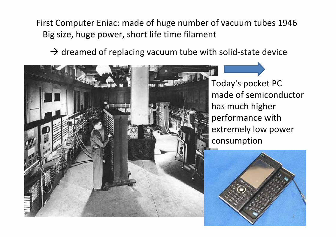
First Computer Eniac: made of huge number of vacuum tubes 1946Big size, huge power, short life time filament
Today's pocket PCmade of semiconductor has much higher performance with extremely low power consumption
dreamed of replacing vacuum tube with solid‐state device
2
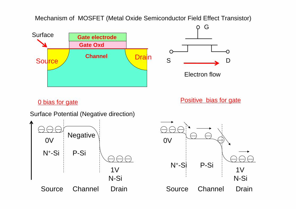
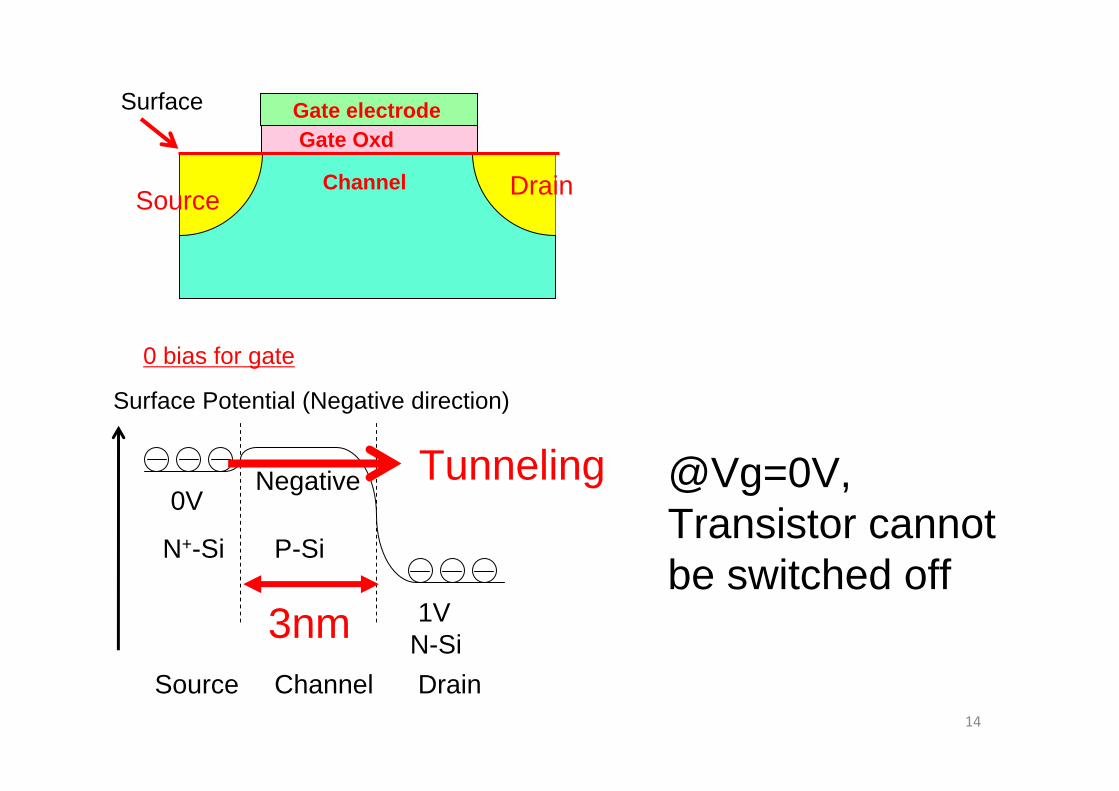
Source Channel Drain
0V
N+-Si P-Si
N-Si
0V
1V
Negative
Source Channel DrainN-Si1V
N+-Si P-Si
Surface Potential (Negative direction)
Gate Oxd
ChannelSource Drain
Gate electrode
S D
G
0 bias for gate Positive bias for gate
Surface
Electron flow
Mechanism of MOSFET (Metal Oxide Semiconductor Field Effect Transistor)
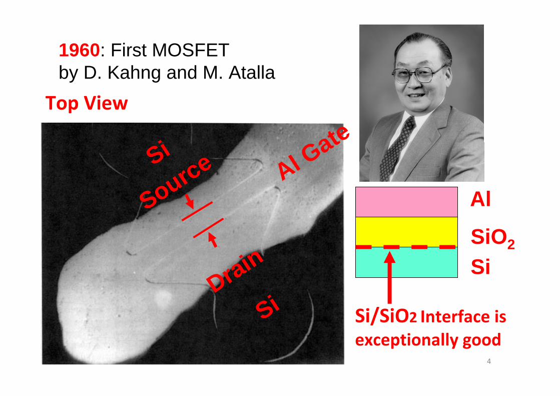
1960: First MOSFET by D. Kahng and M. Atalla
Top View
Al Gate
Source
Drain
Si
Si
Al
SiO2
Si
Si/SiO2 Interface is exceptionally good
4
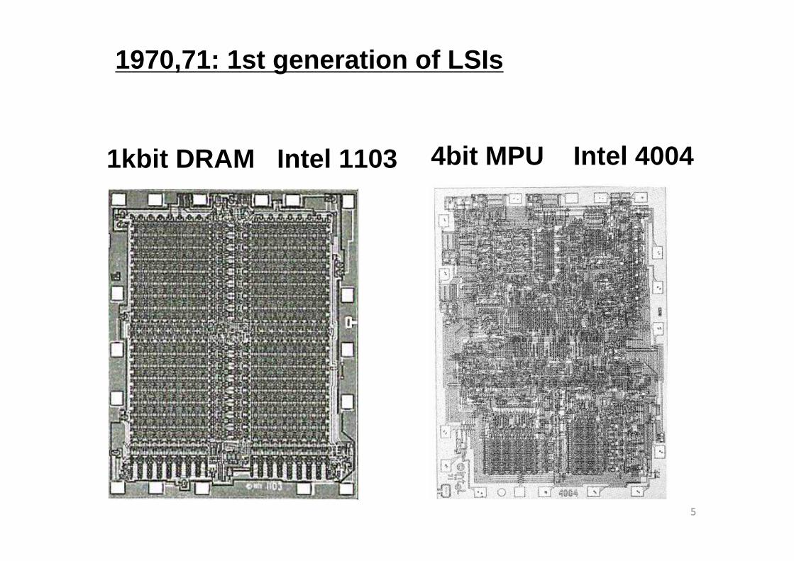
1970,71: 1st generation of LSIs
1kbit DRAM Intel 1103 4bit MPU Intel 4004
5
6
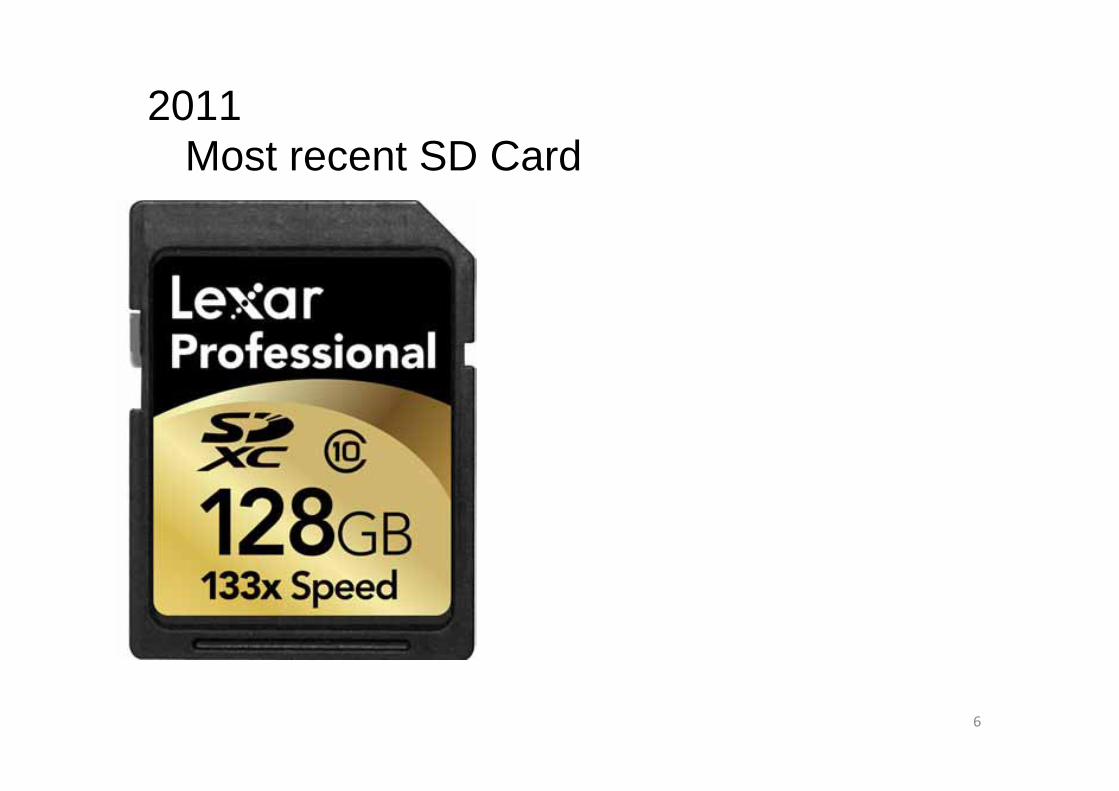
2011Most recent SD Card
7
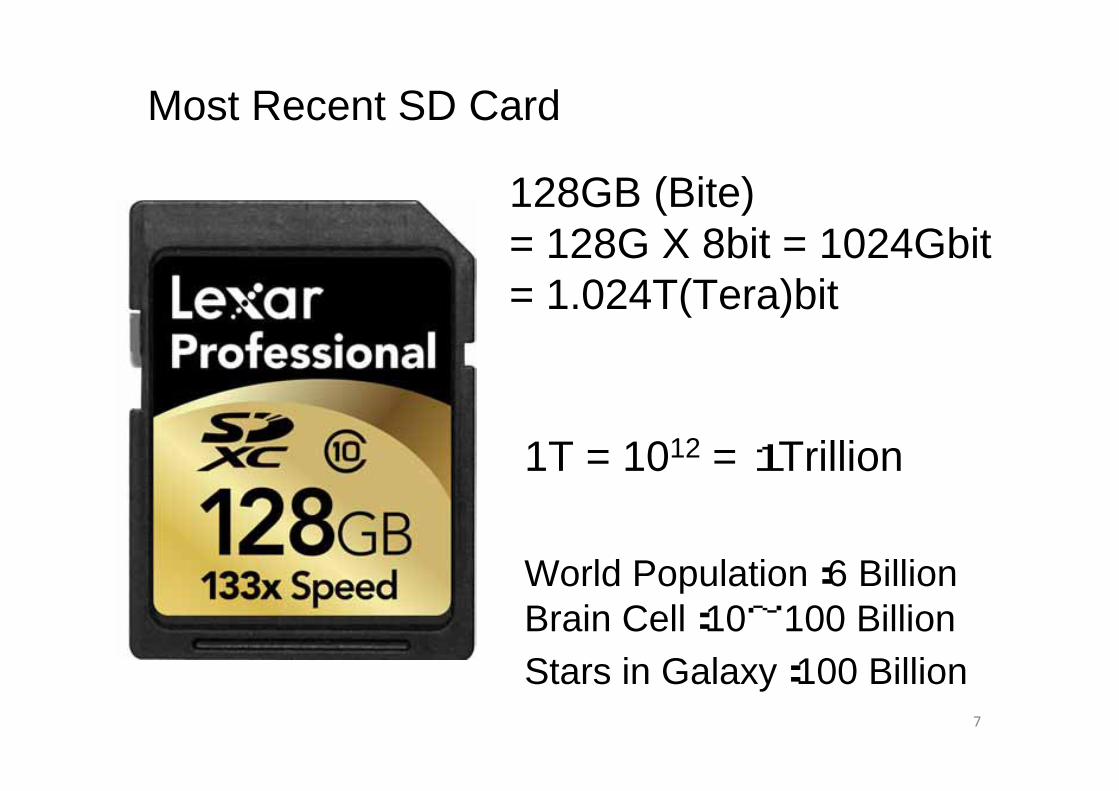
Most Recent SD Card
128GB (Bite) = 128G X 8bit = 1024Gbit= 1.024T(Tera)bit
1T = 1012 = 1Trillion
Brain Cell:10~100 BillionWorld Population:6 Billion
Stars in Galaxy:100 Billion
8
Most Recent SD Card
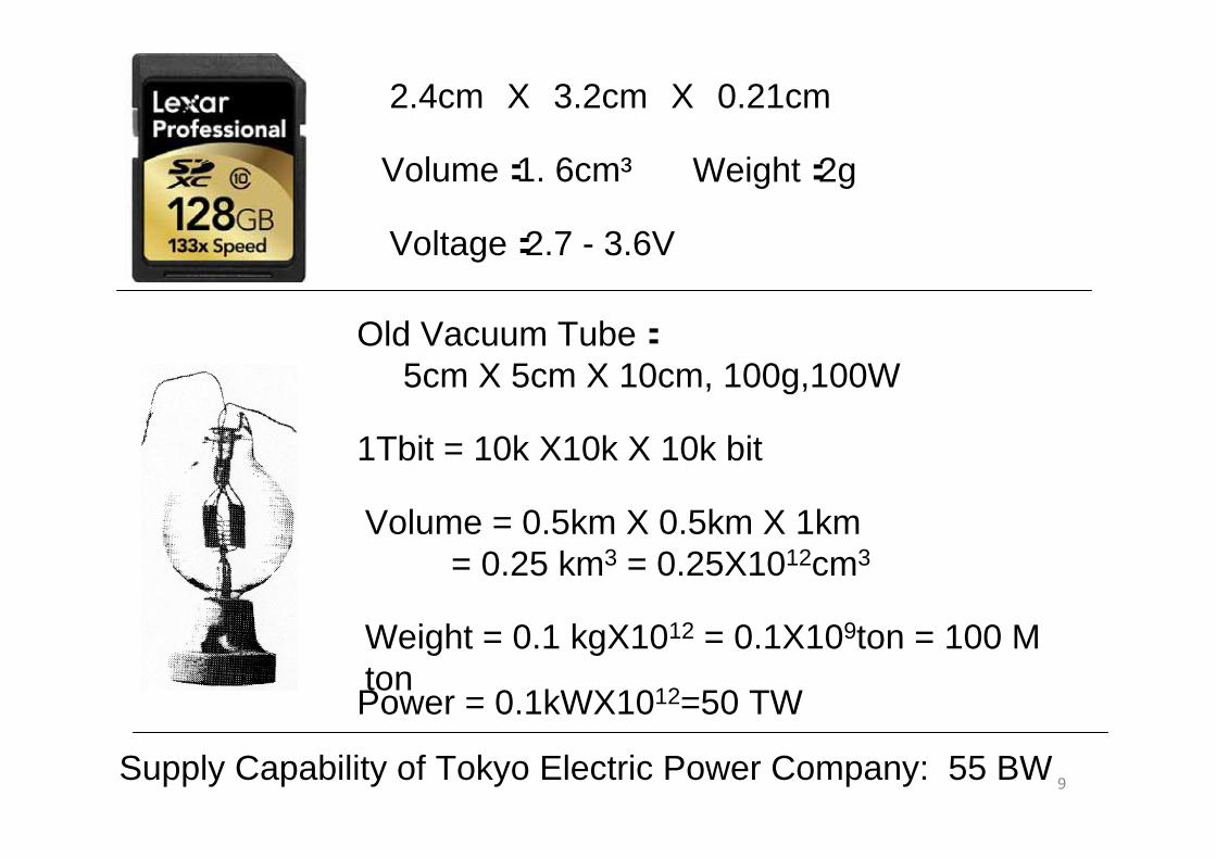
9
2.4cm X 3.2cm X 0.21cm
Volume:1. 6cm³ Weight:2g
Voltage:2.7 - 3.6V
Old Vacuum Tube:5cm X 5cm X 10cm, 100g,100W
1Tbit = 10k X10k X 10k bit
Volume = 0.5km X 0.5km X 1km = 0.25 km3 = 0.25X1012cm3
Weight = 0.1 kgX1012 = 0.1X10⁹ton = 100 M tonPower = 0.1kWX1012=50 TW
Supply Capability of Tokyo Electric Power Company: 55 BW

So, progress of IC technology is most important for the power saving!
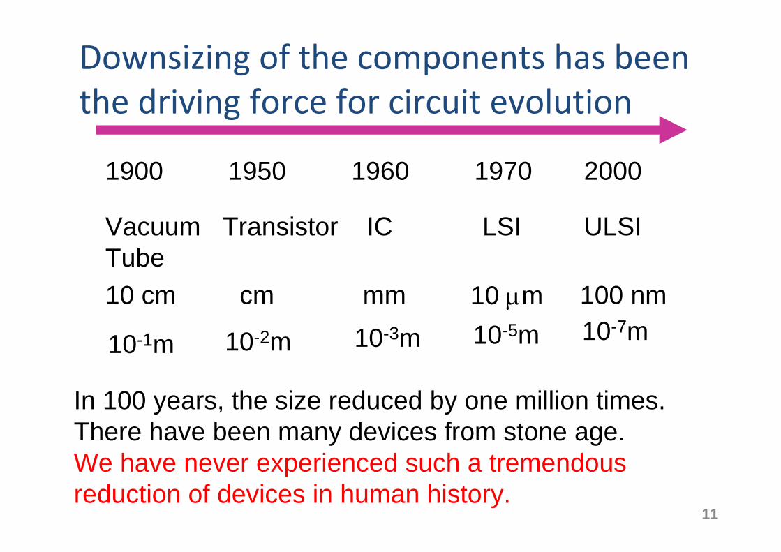
1900 1950 1960 1970 2000
VacuumTube
Transistor IC LSI ULSI
10 cm cm mm 10 µm 100 nm
In 100 years, the size reduced by one million times.There have been many devices from stone age.We have never experienced such a tremendous reduction of devices in human history.
10-1m 10-2m 10-3m 10-5m 10-7m
Downsizing of the components has been the driving force for circuit evolution
11
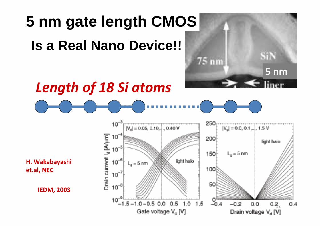
5 nm gate length CMOS
H. Wakabayashi et.al, NEC
IEDM, 2003
Length of 18 Si atoms
Is a Real Nano Device!!
5 nm
12
How far we can go with downscaling?
Question:
Source Channel Drain
N+-Si P-Si
N-Si
0V
1V
Negative
Surface Potential (Negative direction)
Gate Oxd
ChannelSource Drain
Gate electrode
0 bias for gate
Surface
14
Tunneling
3nm
@Vg=0V,Transistor cannotbe switched off
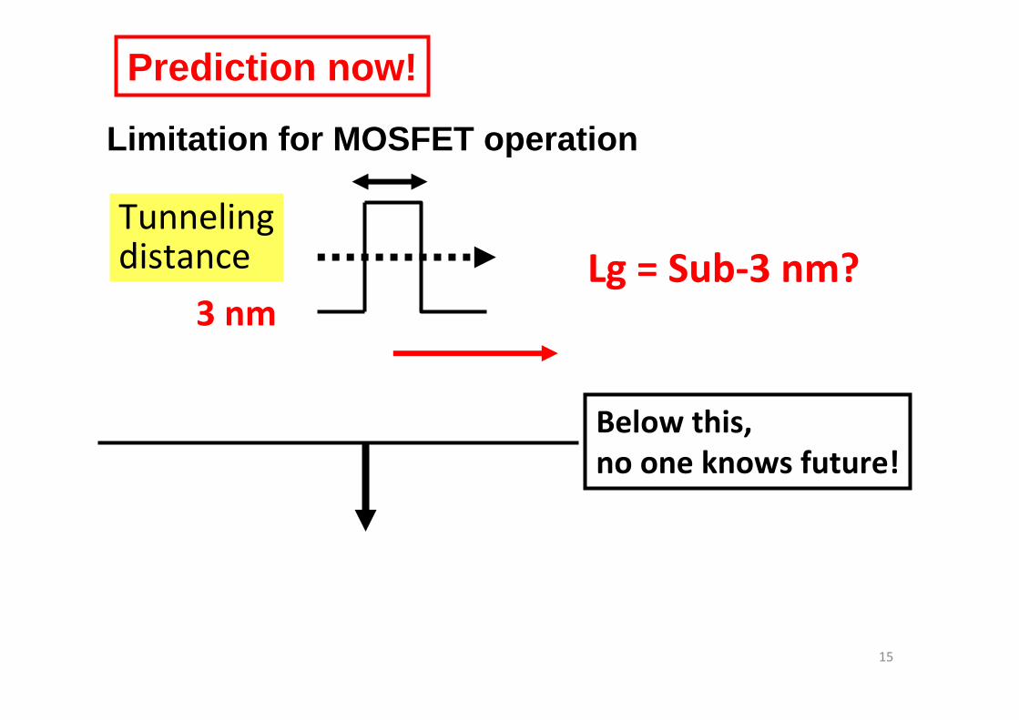
Tunnelingdistance
3 nmLg = Sub‐3 nm?
Below this, no one knows future!
Prediction now!
15
Limitation for MOSFET operation
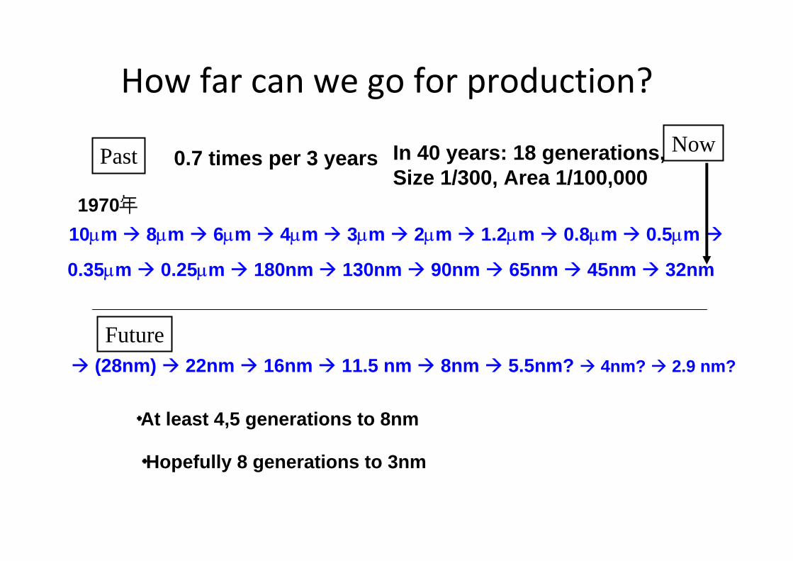
How far can we go for production?
10µm 8µm 6µm 4µm 3µm 2µm 1.2µm 0.8µm 0.5µm
0.35µm 0.25µm 180nm 130nm 90nm 65nm 45nm 32nm
1970年
(28nm) 22nm 16nm 11.5 nm 8nm 5.5nm? 4nm? 2.9 nm?
Past 0.7 times per 3 years NowIn 40 years: 18 generations,Size 1/300, Area 1/100,000
Future
・At least 4,5 generations to 8nm
・Hopefully 8 generations to 3nm
17
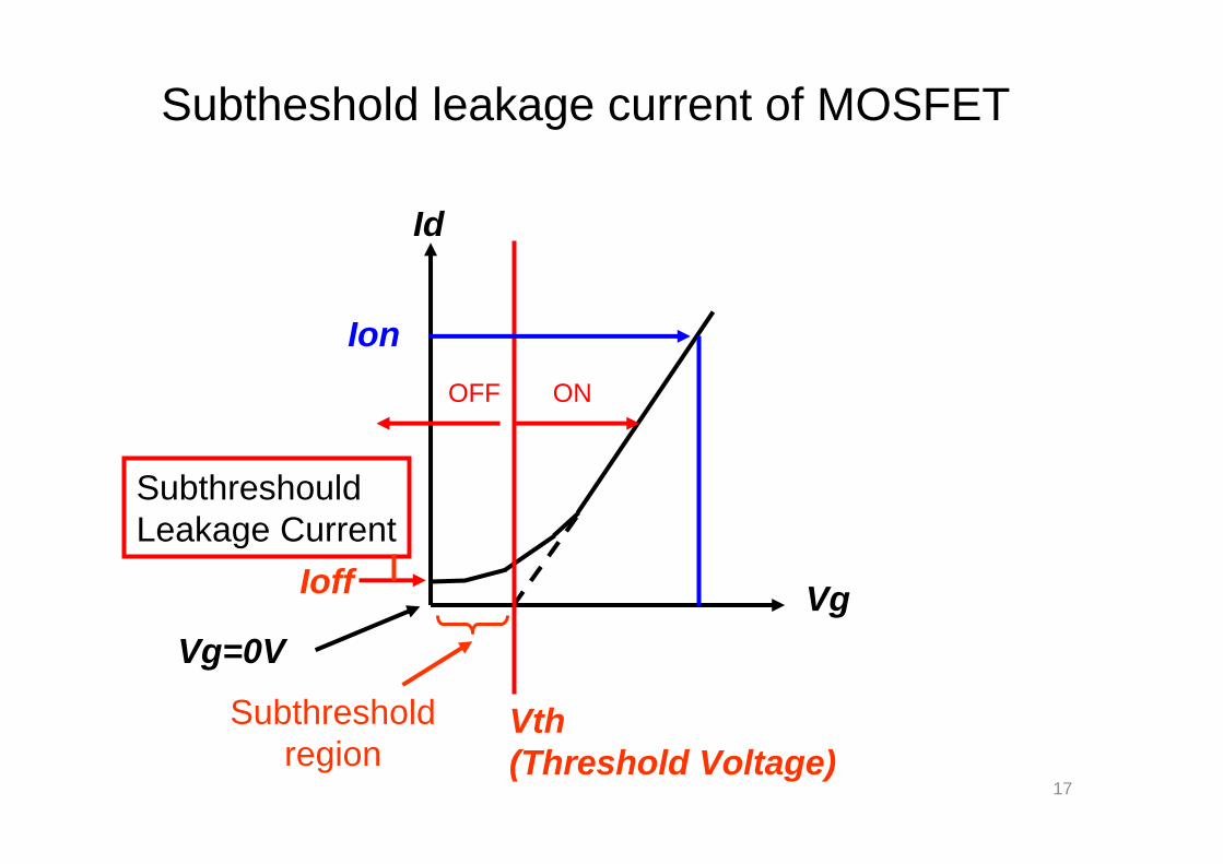
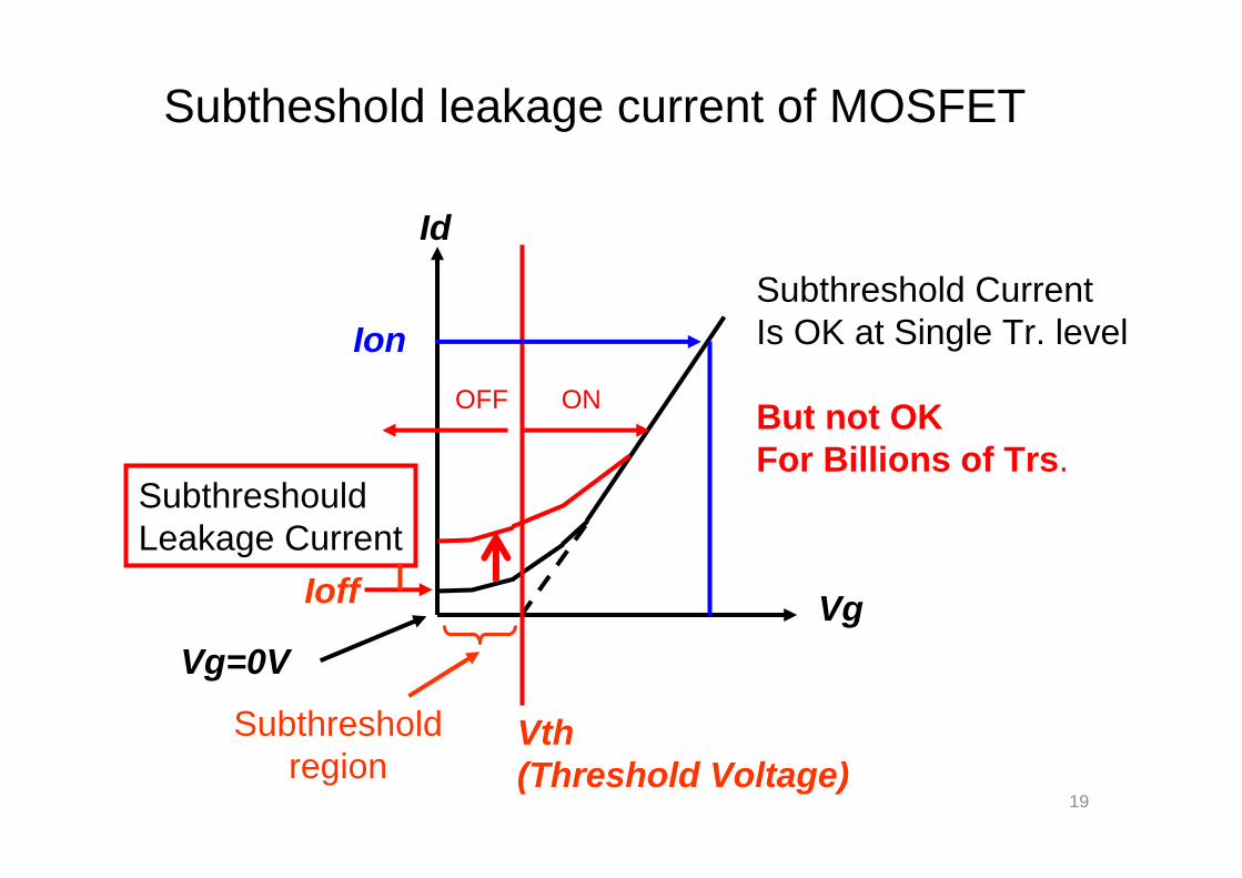
Vg
Id
Vth (Threshold Voltage)
Vg=0V
SubthreshouldLeakage Current
Subtheshold leakage current of MOSFET
ONOFF
Ion
Ioff
Subthresholdregion
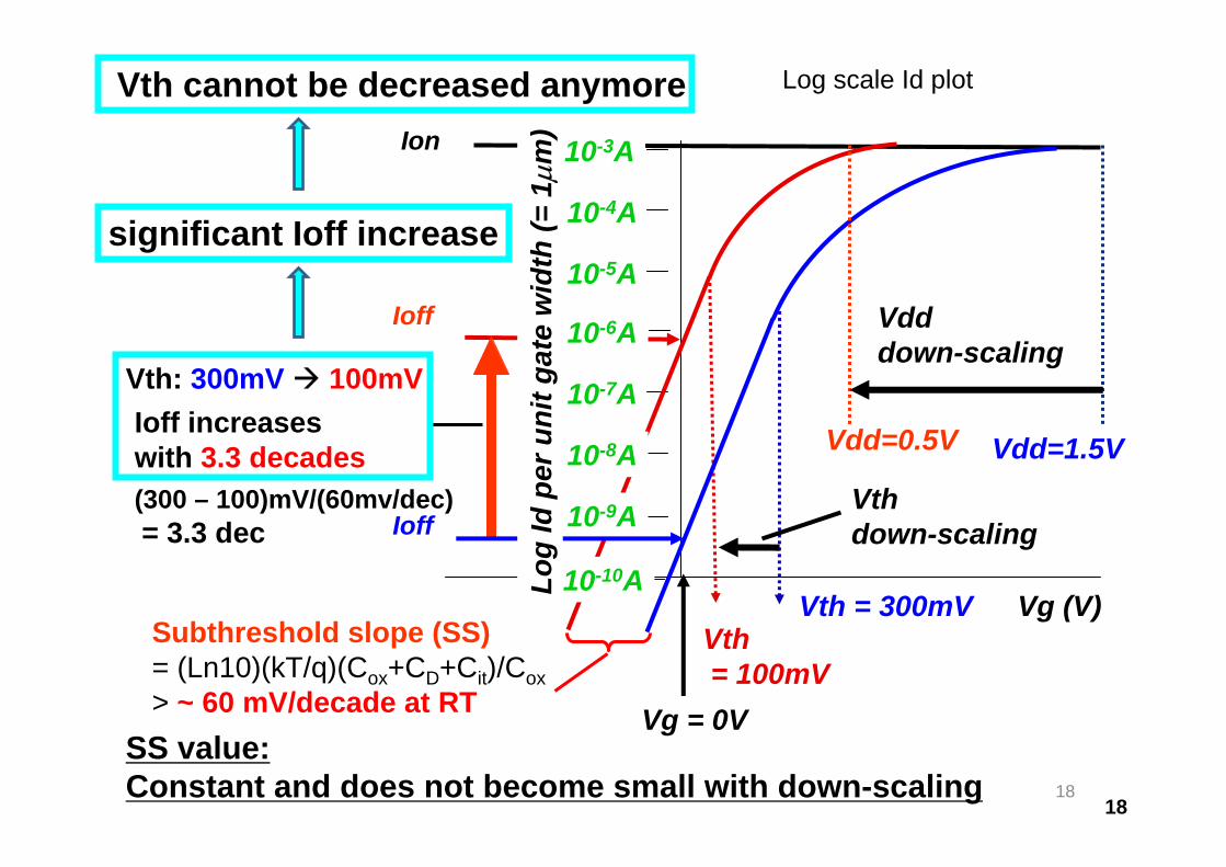
1818
Vg (V)
10-7A
Vg = 0V
Vth = 300mVVth= 100mV
Vth down-scaling
Subthreshold slope (SS)= (Ln10)(kT/q)(Cox+CD+Cit)/Cox> ~ 60 mV/decade at RT
SS value: Constant and does not become small with down-scaling
10-3A
10-4A
10-5A
Vdd=0.5V Vdd=1.5V
Ion
Ioff
Ioff
10-6A
10-8A
10-9A
10-10ALog
Id p
er u
nit g
ate
wid
th (=
1µm
)
Vdd down-scaling
Log scale Id plot
Ioff increaseswith 3.3 decades(300 – 100)mV/(60mv/dec)= 3.3 dec
Vth cannot be decreased anymore
Vth: 300mV 100mV
significant Ioff increase
19
Vg
Id
Vth (Threshold Voltage)
Vg=0V
SubthreshouldLeakage Current
Subtheshold leakage current of MOSFET
Subthreshold CurrentIs OK at Single Tr. level
But not OKFor Billions of Trs.
ONOFF
Ion
Ioff
Subthresholdregion
20
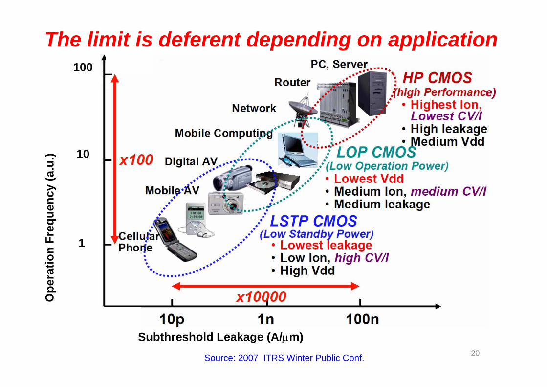
Subthreshold Leakage (A/µm)
Ope
ratio
n Fr
eque
ncy
(a.u
.)
e)
100
10
1
Source: 2007 ITRS Winter Public Conf.
The limit is deferent depending on application
2121
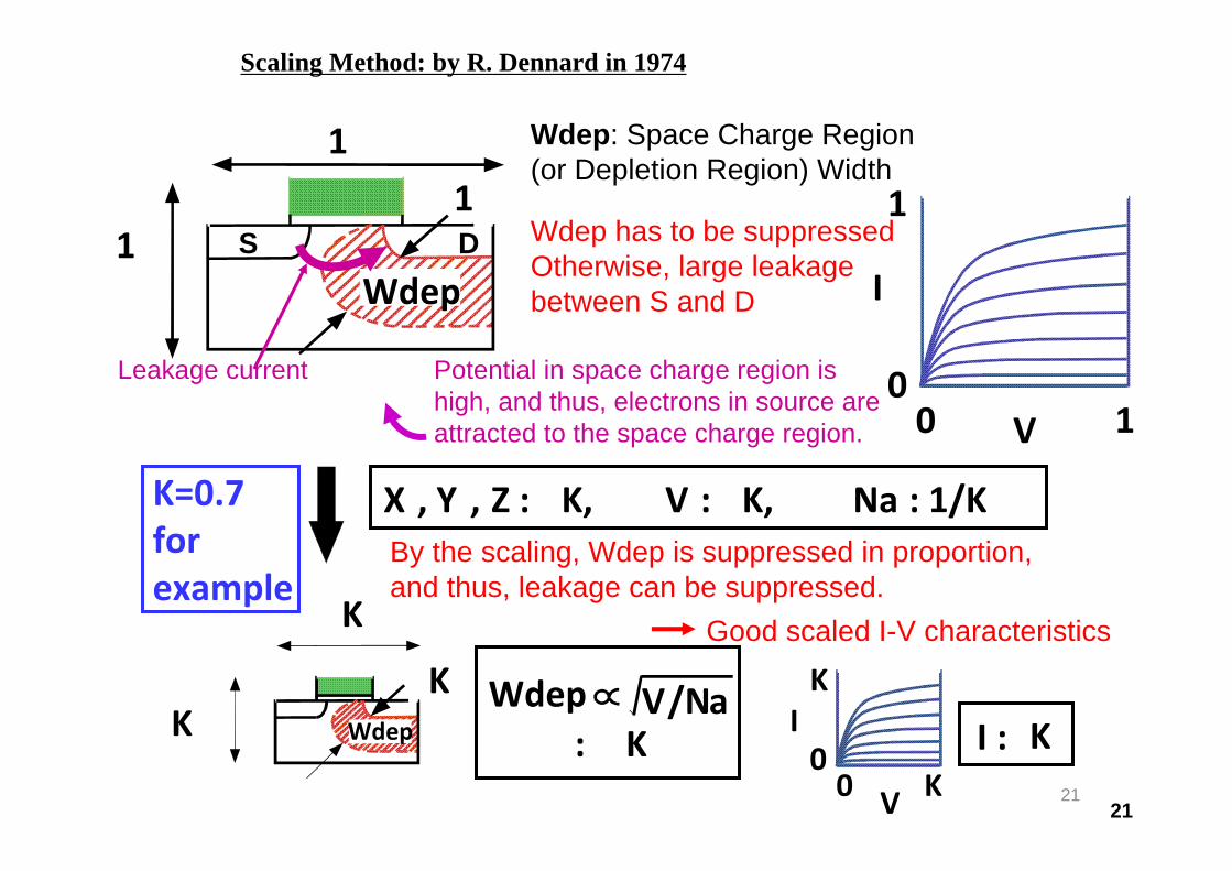
Scaling Method: by R. Dennard in 1974
1
1Wdep
1 1
I
00 V 1
X , Y , Z : K, V : K, Na : 1/K
K
K
KWdep
Wdep V/Na: K
KI00 KV
I : K
K=0.7 for example
Wdep: Space Charge Region (or Depletion Region) Width
Wdep has to be suppressedOtherwise, large leakagebetween S and D
Leakage current
S D
By the scaling, Wdep is suppressed in proportion,and thus, leakage can be suppressed.
Good scaled I-V characteristics
Potential in space charge region ishigh, and thus, electrons in source areattracted to the space charge region.
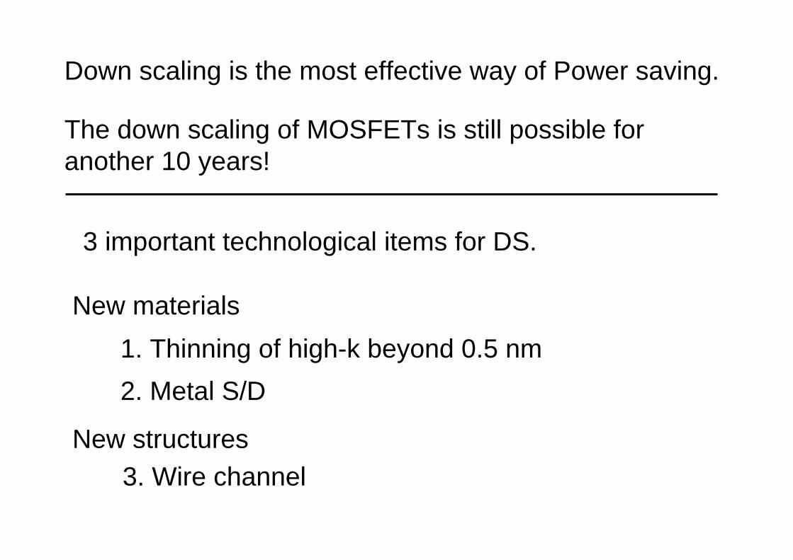
The down scaling of MOSFETs is still possible for another 10 years!
1. Thinning of high-k beyond 0.5 nm2. Metal S/D
3. Wire channel
3 important technological items for DS.
Down scaling is the most effective way of Power saving.
New structures
New materials
1. High-k beyond 0.5 nm
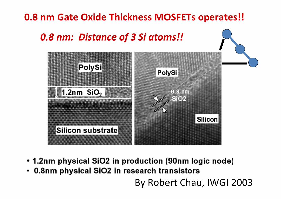
By Robert Chau, IWGI 2003
0.8 nm Gate Oxide Thickness MOSFETs operates!!
0.8 nm: Distance of 3 Si atoms!!
24
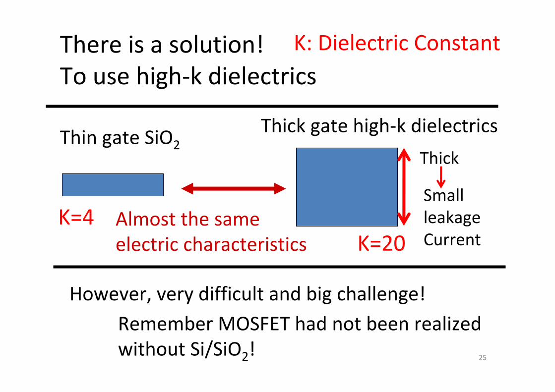
There is a solution!To use high‐k dielectrics
Thin gate SiO2Thick gate high‐k dielectrics
Almost the same electric characteristics
However, very difficult and big challenge!Remember MOSFET had not been realized without Si/SiO2!
K: Dielectric Constant
Thick
Small leakageCurrent
25
K=4K=20
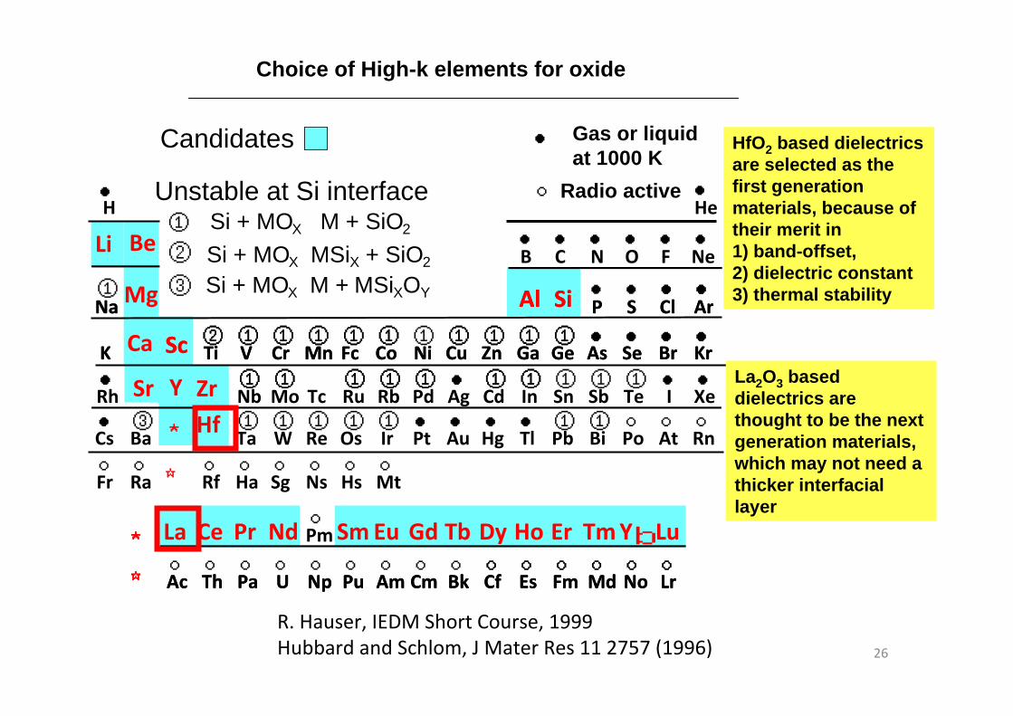
R. Hauser, IEDM Short Course, 1999Hubbard and Schlom, J Mater Res 11 2757 (1996)
Gas or liquidat 1000 K
H
Radio activeHe
Li BeB C N O F Ne
① Na Mg Al Si P S Cl Ar
② ① ① ① ① ① ① ① ① ① ① K Ca Sc Ti V Cr Mn Fc Co Ni Cu Zn Ga Ge As Se Br Kr ① ① ① ① ① ① ① ① ① ① Rh Sr Y Zr Nb Mo Tc Ru Rb Pd Ag Cd In Sn Sb Te I Xe ③ ① ① ① ① ① ① ① Cs Ba
HfTa W Re Os Ir Pt Au Hg Tl Pb Bi Po At Rn
Fr Ra Rf Ha Sg Ns Hs Mt
La Ce Pr Nd PmSmEu Gd Tb Dy Ho Er TmYb Lu Ac Th Pa U Np Pu Am Cm Bk Cf Es Fm Md No Lr
Candidates
Na Al Si P S Cl Ar
② ① ① ① ① ① ① ① ① ① K Sc Ti V Cr Mn Fc Co Ni Cu Zn Ga Ge As Se Br Kr ① ① ① ① ① ① ①
Ac Th Pa U Np Pu Am Cm Bk Cf Es Fm Md No Lr
②
③
Unstable at Si interfaceSi + MOX M + SiO2①
Si + MOX MSiX + SiO2
Si + MOX M + MSiXOY
Choice of High-k elements for oxide
HfO2 based dielectrics are selected as the first generation materials, because of their merit in1) band-offset, 2) dielectric constant3) thermal stability
La2O3 based dielectrics are thought to be the next generation materials, which may not need a thicker interfacial layer
26
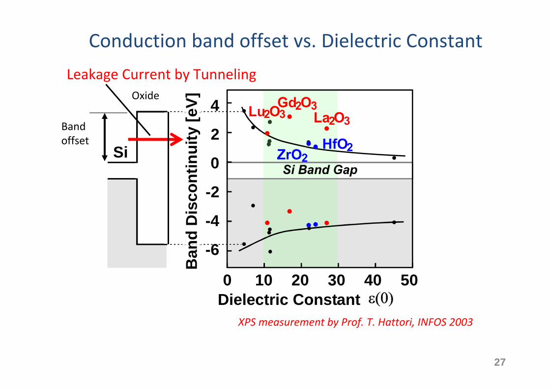
0 10 20 30 40 50Dielectric Constant
4
2
0
-2
-4
-6
SiO2
Ban
d D
isco
ntin
uity
[eV]
Si
XPS measurement by Prof. T. Hattori, INFOS 2003
Conduction band offset vs. Dielectric Constant
Band offset
Oxide
Leakage Current by Tunneling
27
28
PMOS
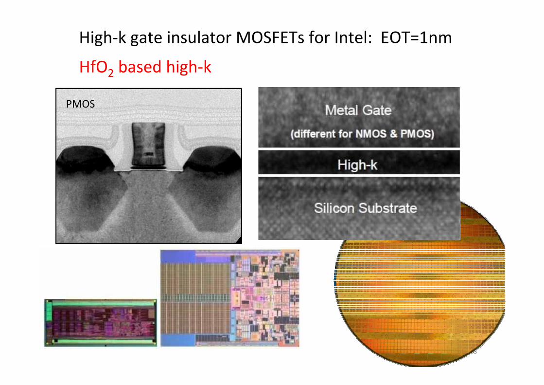
High‐k gate insulator MOSFETs for Intel: EOT=1nm
HfO2 based high‐k
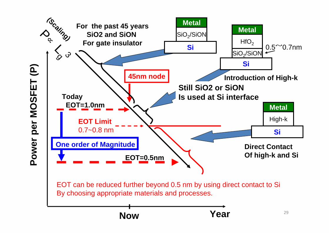
29Year
Pow
er p
er M
OSF
ET (P
)
P∝L
g 3
(Scaling)
EOT Limit0.7~0.8 nm
EOT=0.5nm
TodayEOT=1.0nm
Now
45nm node
One order of Magnitude
Si
HfO2
Metal
SiO2/SiON
Si
High-k
Metal
Direct ContactOf high-k and Si
Si
MetalSiO2/SiON
0.5~0.7nm
Introduction of High-kStill SiO2 or SiONIs used at Si interface
For the past 45 yearsSiO2 and SiON
For gate insulator
EOT can be reduced further beyond 0.5 nm by using direct contact to SiBy choosing appropriate materials and processes.
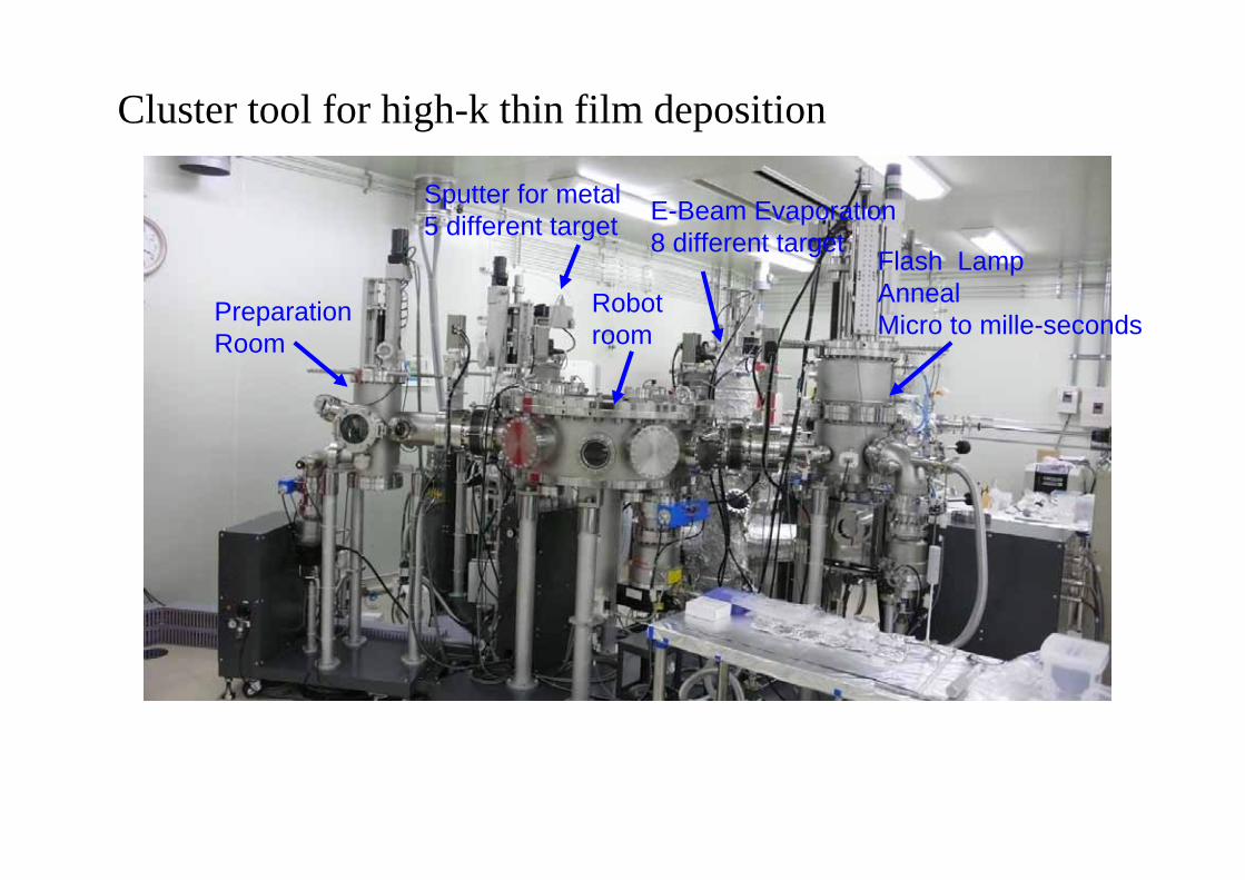
PreparationRoom
E-Beam Evaporation8 different target
Flash LampAnnealMicro to mille-seconds
Sputter for metal5 different target
Robot room
Cluster tool for high-k thin film deposition
31
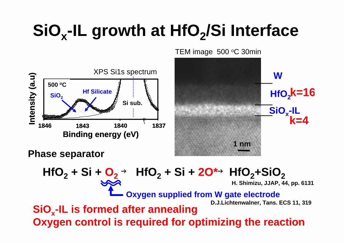
1837184018431846Binding energy (eV)
Inte
nsity
(a.u
)
Si sub.
Hf SilicateSiO2
500 oC
1837184018431846Binding energy (eV)
Inte
nsity
(a.u
)
Si sub.
Hf SilicateSiO2
500 oC
SiOx-IL
HfO2
W
1 nm
k=4
k=16
SiOx-IL growth at HfO2/Si Interface
HfO2 + Si + O2→ HfO2 + Si + 2O*→HfO2+SiO2
Phase separator
SiOx-IL is formed after annealingOxygen control is required for optimizing the reaction
Oxygen supplied from W gate electrode
XPS Si1s spectrum
D.J.Lichtenwalner, Tans. ECS 11, 319
TEM image 500 oC 30min
H. Shimizu, JJAP, 44, pp. 6131
32
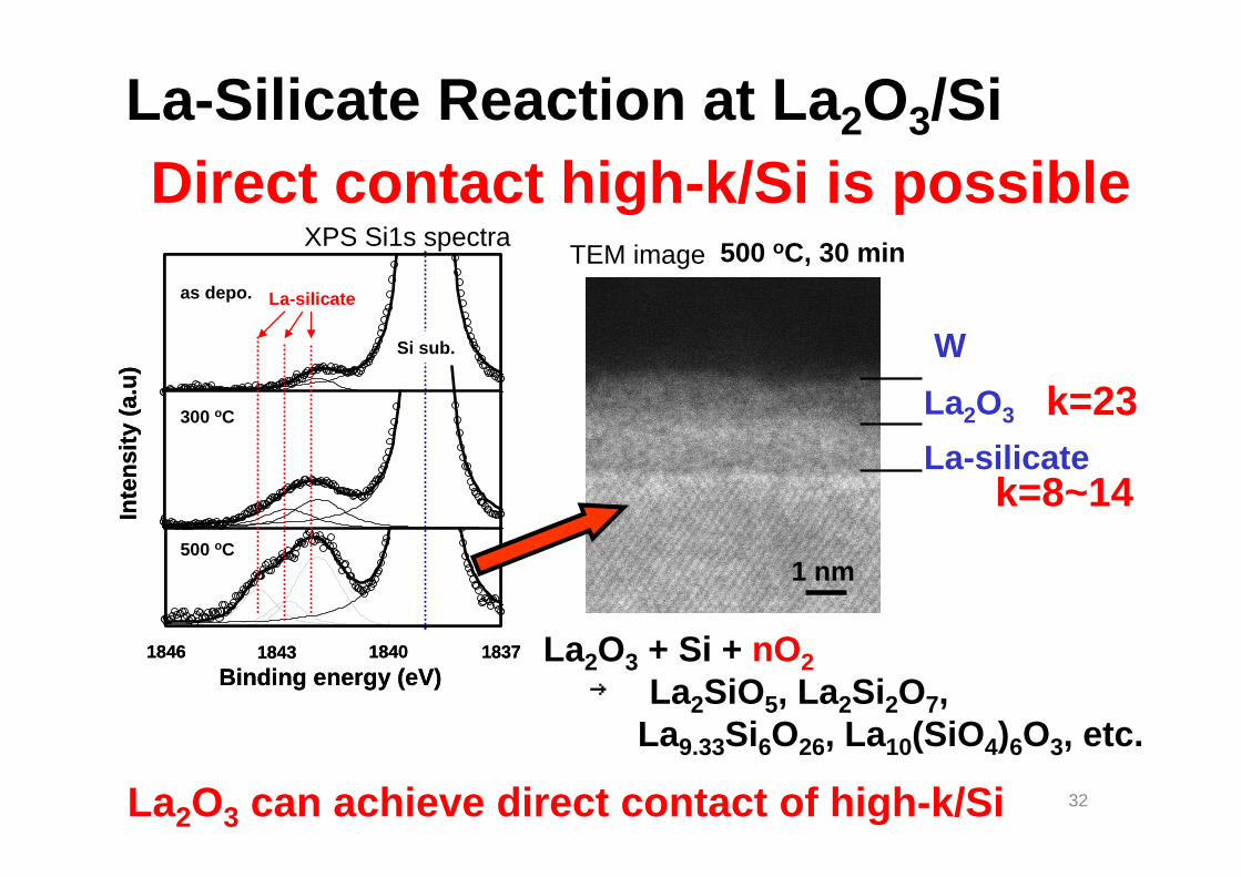
La-Silicate Reaction at La2O3/Si
La2O3
La-silicate
W
500 oC, 30 min
1 nm
k=8~14
k=23
1837184018431846Binding energy (eV)
Inte
nsity
(a.u
)
as depo.
300 oC
La-silicate
Si sub.
500 oC
1837184018431846Binding energy (eV)
Inte
nsity
(a.u
)
as depo.
300 oC
La-silicate
Si sub.
500 oC
La2O3 + Si + nO2→ La2SiO5, La2Si2O7,
La9.33Si6O26, La10(SiO4)6O3, etc.
La2O3 can achieve direct contact of high-k/Si
XPS Si1s spectraTEM image
Direct contact high-k/Si is possible
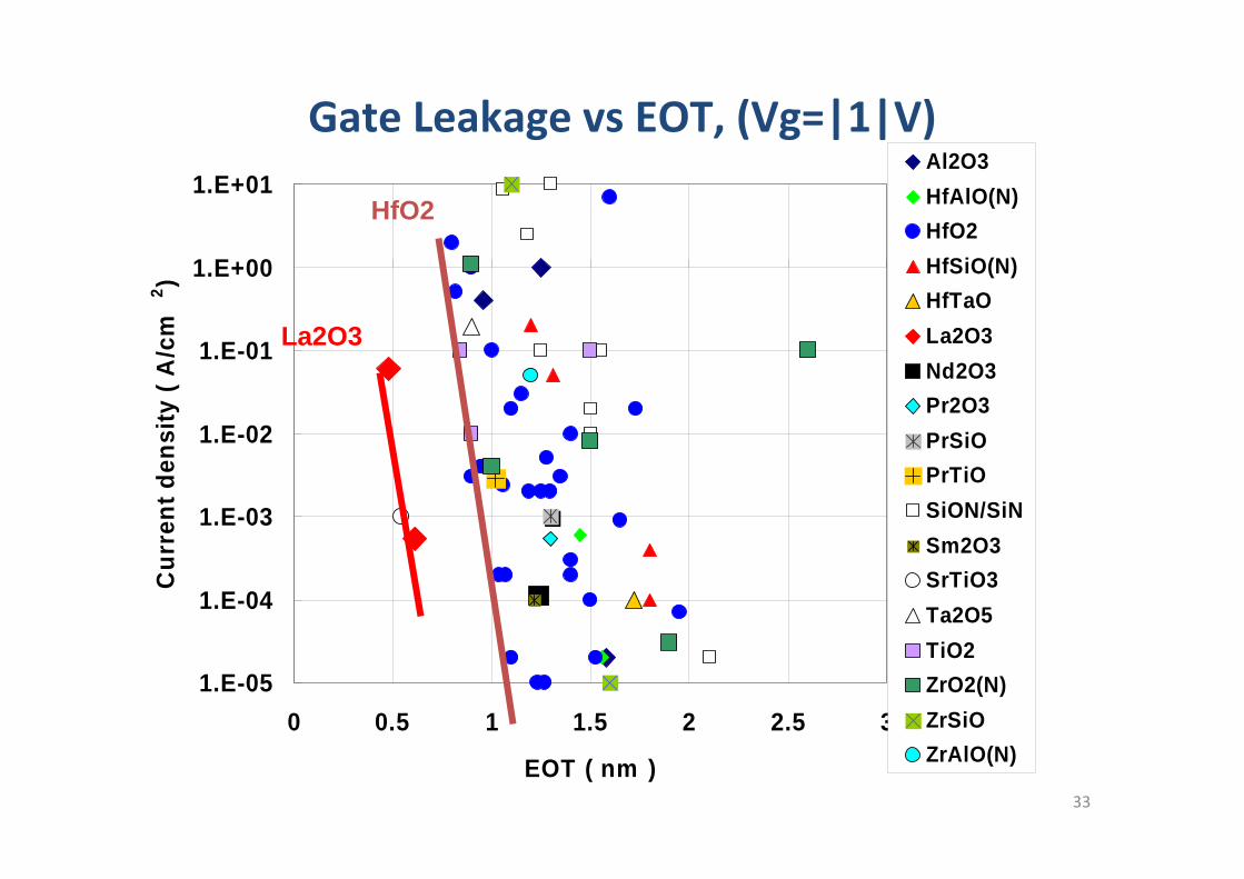
1.E-05
1.E-04
1.E-03
1.E-02
1.E-01
1.E+00
1.E+01
0 0.5 1 1.5 2 2.5 3
EOT ( nm )
Cur
rent
den
sity
( A
/cm
2 )Al2O3HfAlO(N)HfO2HfSiO(N)HfTaOLa2O3Nd2O3Pr2O3PrSiOPrTiOSiON/SiNSm2O3SrTiO3Ta2O5TiO2ZrO2(N)ZrSiOZrAlO(N)
Gate Leakage vs EOT, (Vg=|1|V)
La2O3
HfO2
33
34
0.0E+00
5.0E-04
1.0E-03
1.5E-03
2.0E-03
2.5E-03
3.0E-03
3.5E-03
0 0.2 0.4 0.6 0.8 1
Vg=0VVg=0.2VVg=0.4VVg=0.6VVg=0.8VVg=1.0VVg=1.2V
0 0.2 0.4 0.6 0.8 1
Vg=0VVg=0.2VVg=0.4VVg=0.6VVg=0.8VVg=1.0VVg=1.2V
0 0.2 0.4 0.6 0.8 1
Vg=0VVg=0.2VVg=0.4VVg=0.6VVg=0.8VVg=1.0VVg=1.2VI d
(V)
W/L = 50µm /2.5µm
Vd (V) Vd (V) Vd (V)
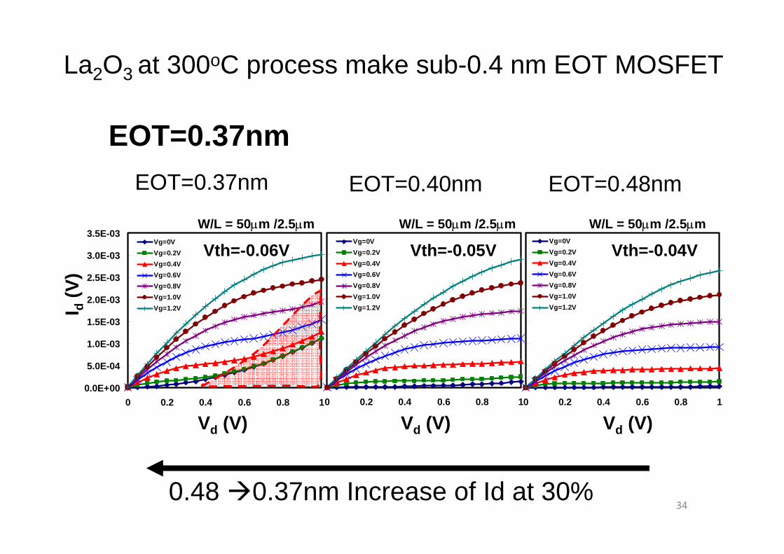
EOT=0.37nm
Vth=-0.04VVth=-0.05VVth=-0.06V
EOT=0.37nm EOT=0.40nm EOT=0.48nmW/L = 50µm /2.5µm W/L = 50µm /2.5µm
0.48 0.37nm Increase of Id at 30%
La2O3 at 300oC process make sub-0.4 nm EOT MOSFET
35
2
1.5
1
0.5
0
Cap
acita
nce
[µF/
cm2 ]
-1 -0.5 0 0.5 1Gate Voltage [V]
10kHz 100kHz 1MHz
20 x 20µm2 1.5
1
0.5
0
Cap
acita
nce
[µF/
cm2 ]
-1.5 -1 -0.5 0 0.5Gate Voltage [V]
20 x 20µm2
10kHz 100kHz 1MHz
2
1.5
1
0.5
0
Cap
acita
nce
[µF/
cm2 ]
-1.5 -1 -0.5 0 0.5Gate Voltage [V]
20 x 20µm2
10kHz 100kHz 1MHz
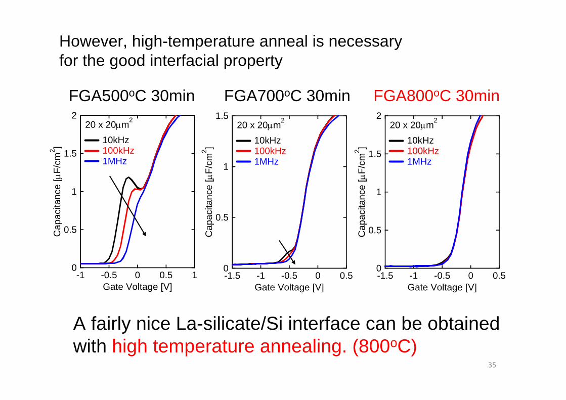
FGA500oC 30min FGA700oC 30min FGA800oC 30min
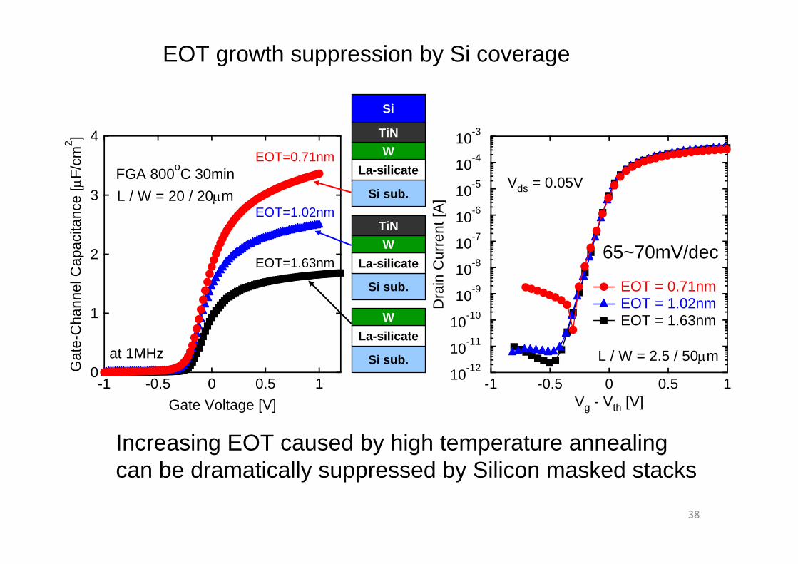
A fairly nice La-silicate/Si interface can be obtained with high temperature annealing. (800oC)
However, high-temperature anneal is necessary for the good interfacial property
36
500
400
300
200
100
0
Ele
ctro
n M
obili
ty [c
m2 /V
sec]
10.80.60.40.20Eeff [MV/cm]
FGA 800oC FGA 700oC FGA 500oC
Universal
Nsub = 3 x 1016 cm-3T = 300K
EOT~1.3nm
Pulse input
10-9
10-8
10-7
10-6
Cha
rge
pum
ping
cur
rent
[A]
104 105 106
Frequency [Hz]
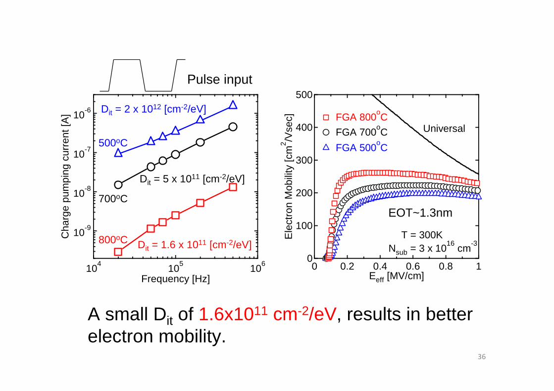
Dit = 2 x 10¹² [cm-2/eV]
Dit = 5 x 10¹¹ [cm-2/eV]
Dit = 1.6 x 10¹¹ [cm-2/eV]
500oC
700oC
800oC
A small Dit of 1.6x1011 cm-2/eV, results in better electron mobility.
37
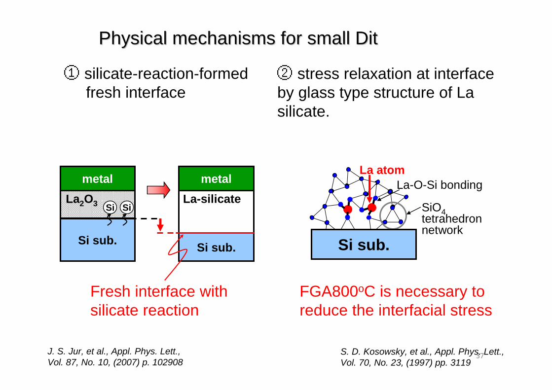
① silicate-reaction-formedfresh interface
metal
Si sub.
metal
Si sub.
La2O3 La-silicateSi Si
Fresh interface with silicate reaction
J. S. Jur, et al., Appl. Phys. Lett., Vol. 87, No. 10, (2007) p. 102908
② stress relaxation at interface by glass type structure of La silicate.
La atomLa-O-Si bonding
Si sub.
SiO4tetrahedron network
FGA800oC is necessary to reduce the interfacial stress
S. D. Kosowsky, et al., Appl. Phys. Lett., Vol. 70, No. 23, (1997) pp. 3119
Physical mechanisms for small DitPhysical mechanisms for small Dit
38
4
3
2
1
0Gat
e-C
hann
el C
apac
itanc
e [µ
F/cm
2 ]
10.50-0.5-1Gate Voltage [V]
at 1MHz
L / W = 20 / 20µmFGA 800oC 30min
Si sub.
La-silicateW
Si sub.
La-silicateW
TiN
Si sub.
La-silicateW
TiN
Si
EOT=1.02nm
EOT=1.63nm
EOT=0.71nm
10-12
10-11
10-10
10-9
10-8
10-7
10-6
10-5
10-4
10-3
Dra
in C
urre
nt [A
]
-1 -0.5 0 0.5 1Vg - Vth [V]
L / W = 2.5 / 50µm
Vds = 0.05V
EOT = 0.71nm EOT = 1.02nm EOT = 1.63nm
65~70mV/dec
Increasing EOT caused by high temperature annealing can be dramatically suppressed by Silicon masked stacks
EOT growth suppression by Si coverage

39
No interfacial layer can be confirmed with Si/TiN/W
MIPSW TiN/W
Kav ~ 8 Kav ~ 12 Kav ~ 16
Si 2nm2nm2nm
HK
MG
La2O3Si/TiN/W
40
4
3
2
1
0Gat
e-C
hann
el C
apac
itanc
e [µ
F/cm
2 ]
10.50-0.5Gate Voltage [V]
FGA 800oC 30minL / W = 10 / 10µm
10kHz 100kHz 1MHz
200
150
100
50
0
Ele
ctro
n M
obili
ty [c
m2 /V
sec]
1.510.50Eeff [MV/cm]
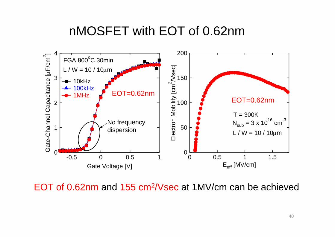
L / W = 10 / 10µmNsub = 3 x 1016 cm-3T = 300K
EOT=0.62nmEOT=0.62nm
No frequency dispersion
EOT of 0.62nm and 155 cm2/Vsec at 1MV/cm can be achieved
nMOSFET with EOT of 0.62nm
41
10-2
10-1
100
101
102
103
104
J g a
t Vg
= 1V
[A/c
m2 ]
0.80.750.70.650.60.550.5EOT [nm]
A = 10 x 10µm2
ITRS requirements
MIPS Stacks
300
250
200
150
100
50
0
Ele
ctro
n M
obili
ty [c
m2 /V
sec]
1.31.21.110.90.80.70.60.5EOT [nm]
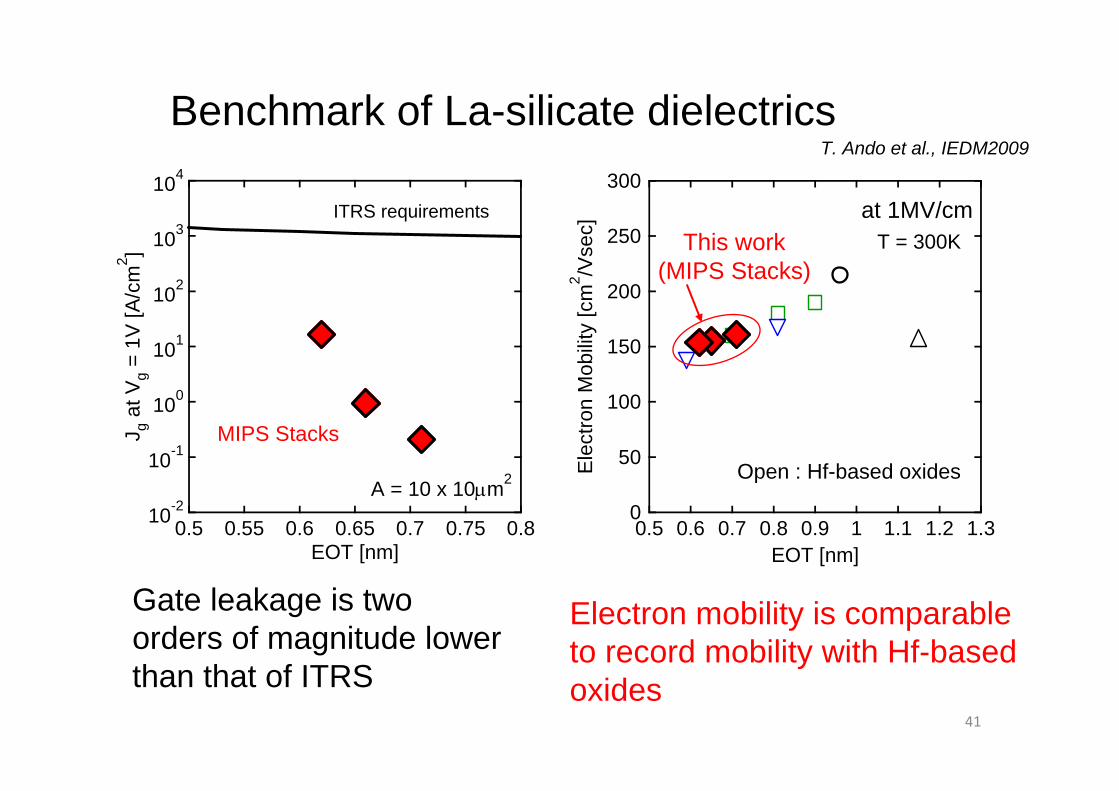
at 1MV/cmT = 300KThis work
(MIPS Stacks)
Open : Hf-based oxides
T. Ando et al., IEDM2009
Gate leakage is two orders of magnitude lower than that of ITRS
Electron mobility is comparable to record mobility with Hf-based oxides
Benchmark of La-silicate dielectrics
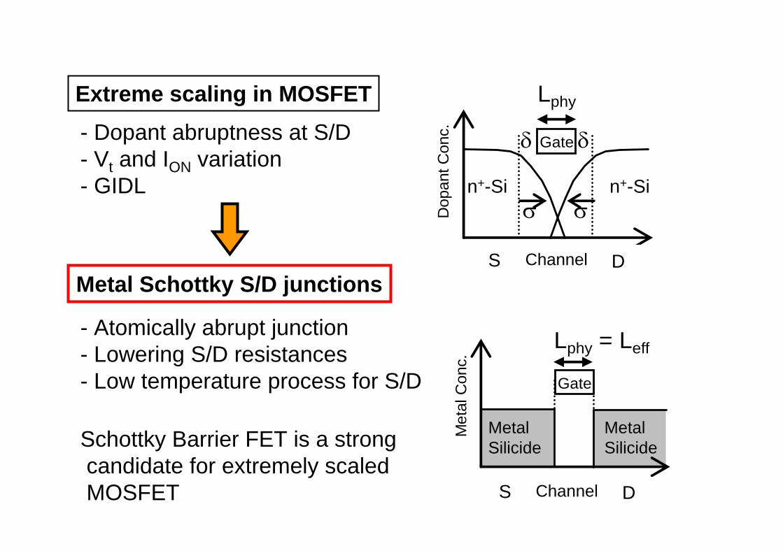
Metal (Silicide) S/D
Extreme scaling in MOSFET Lphy
Dop
antC
onc. δ δGate
σ σ
Met
al C
onc.
Gate
Lphy = Leff- Atomically abrupt junction- Lowering S/D resistances- Low temperature process for S/D
Metal Schottky S/D junctions
- Dopant abruptness at S/D- Vt and ION variation- GIDL
Schottky Barrier FET is a strong candidate for extremely scaled MOSFET S DChannel
S DChannel
n+-Sin+-Si
Metal Silicide
Metal Silicide
44
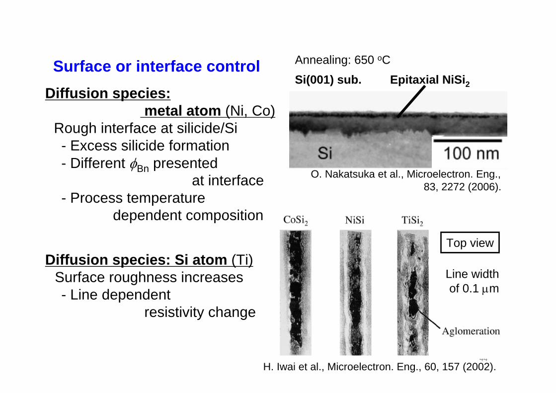
Surface or interface controlDiffusion species:
metal atom (Ni, Co)Rough interface at silicide/Si- Excess silicide formation- Different φBn presented
at interface- Process temperature
dependent composition
Diffusion species: Si atom (Ti)Surface roughness increases- Line dependent
resistivity change
Line widthof 0.1 µm
H. Iwai et al., Microelectron. Eng., 60, 157 (2002).
Top view
Epitaxial NiSi2
O. Nakatsuka et al., Microelectron. Eng.,83, 2272 (2006).
Si(001) sub.Annealing: 650 oC
45
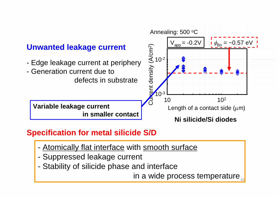
Unwanted leakage current
- Atomically flat interface with smooth surface- Suppressed leakage current- Stability of silicide phase and interface
in a wide process temperature
Specification for metal silicide S/D
- Edge leakage current at periphery- Generation current due to
defects in substrate
Length of a contact side (µm)
Cur
rent
den
sity
(A/c
m2 )
10-3
10-2
10 102
Vapp = -0.2V φBn = ~0.57 eV
Variable leakage currentin smaller contact
Ni silicide/Si diodes
Annealing: 500 oC
46
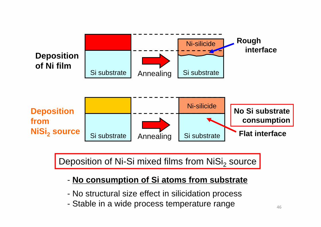
Si substrate
Ni-silicide
Si substrate
Si substrate
Ni-silicide
Si substrate
Deposition of Ni film
Deposition fromNiSi2 source Annealing Flat interface
Roughinterface
No Si substrateconsumption
Annealing
Deposition of Ni-Si mixed films from NiSi2 source
- No consumption of Si atoms from substrate- No structural size effect in silicidation process- Stable in a wide process temperature range
47
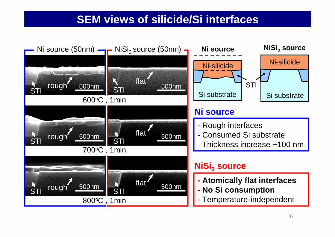
SEM views of silicide/Si interfaces
NiSi2 source
Ni source (50nm)
rough
rough
rough flat
flat
flat
STI 500nm
NiSi2 source (50nm)
500nm
500nm
STI
500nmSTI STI
500nmSTI500nmSTI600oC , 1min
700oC , 1min
800oC , 1min
- Rough interfaces- Consumed Si substrate - Thickness increase ~100 nm
Ni source
- Atomically flat interfaces- No Si consumption- Temperature-independent
Si substrate
Ni-silicide
Ni source
Ni-silicide
Si substrate
NiSi2 source
STI
48
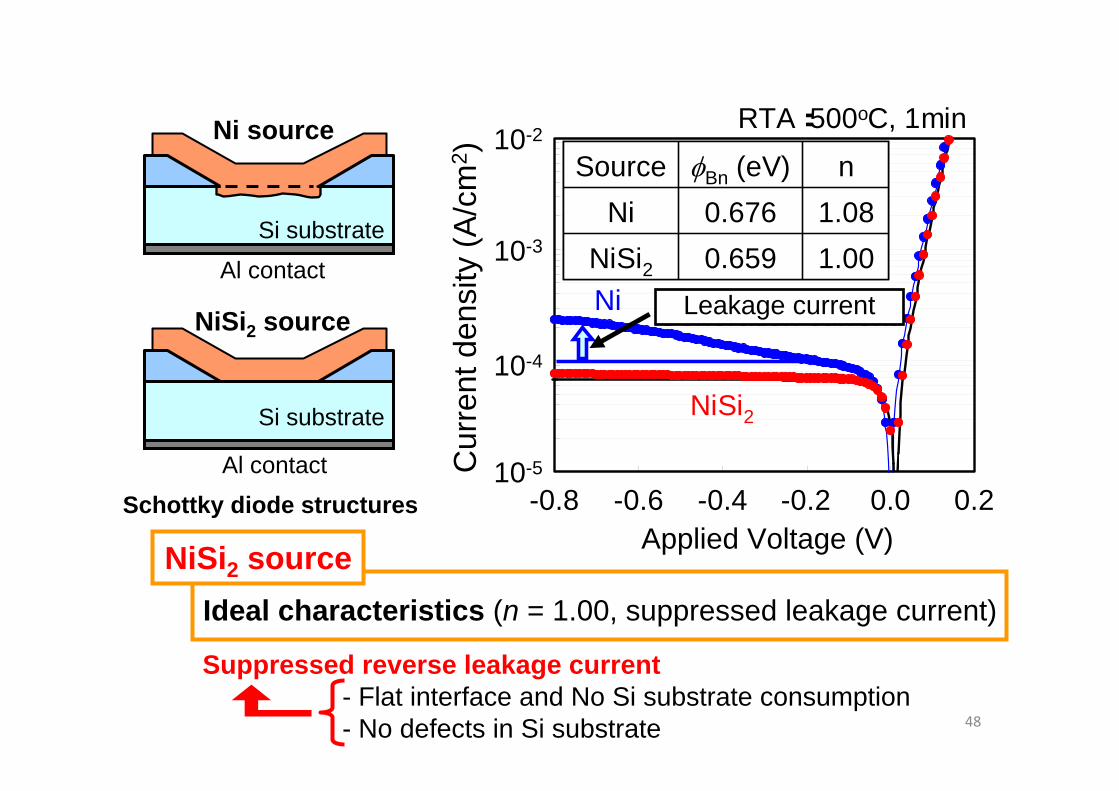
Ideal characteristics (n = 1.00, suppressed leakage current)
Suppressed reverse leakage current- Flat interface and No Si substrate consumption- No defects in Si substrate
Ni
NiSi2
-0.8 -0.6 0.0 0.2Diode voltage (V)
-0.4 -0.210-5
10-4
10-3
10-2
Dio
de c
urre
nt (A
/cm
2 )
1.001.08
n
0.659NiSi2
0.676NiφBn (eV)Source
1.001.08
n
0.659NiSi2
0.676NiφBn (eV)Source
Generation current
RTA:500oC, 1min
Schottky diode structures
Leakage currentAl contact
Ni source
Al contact
NiSi2 source
Si substrate
Si substrate
NiSi2 source Applied Voltage (V)
Cur
rent
den
sity
(A/c
m2 )

Wire channel
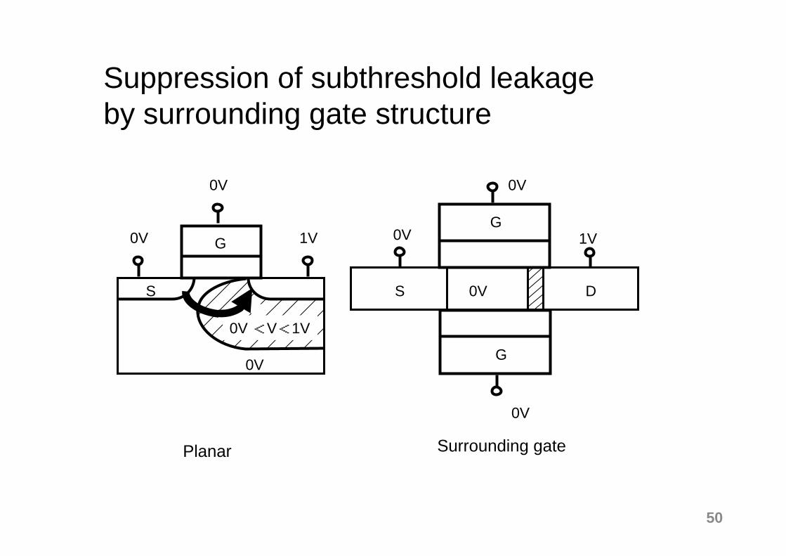
50
1V0V
0V
S
0V
0V <V<1V
1V0V
0V
0V
0VS D
G
G
G
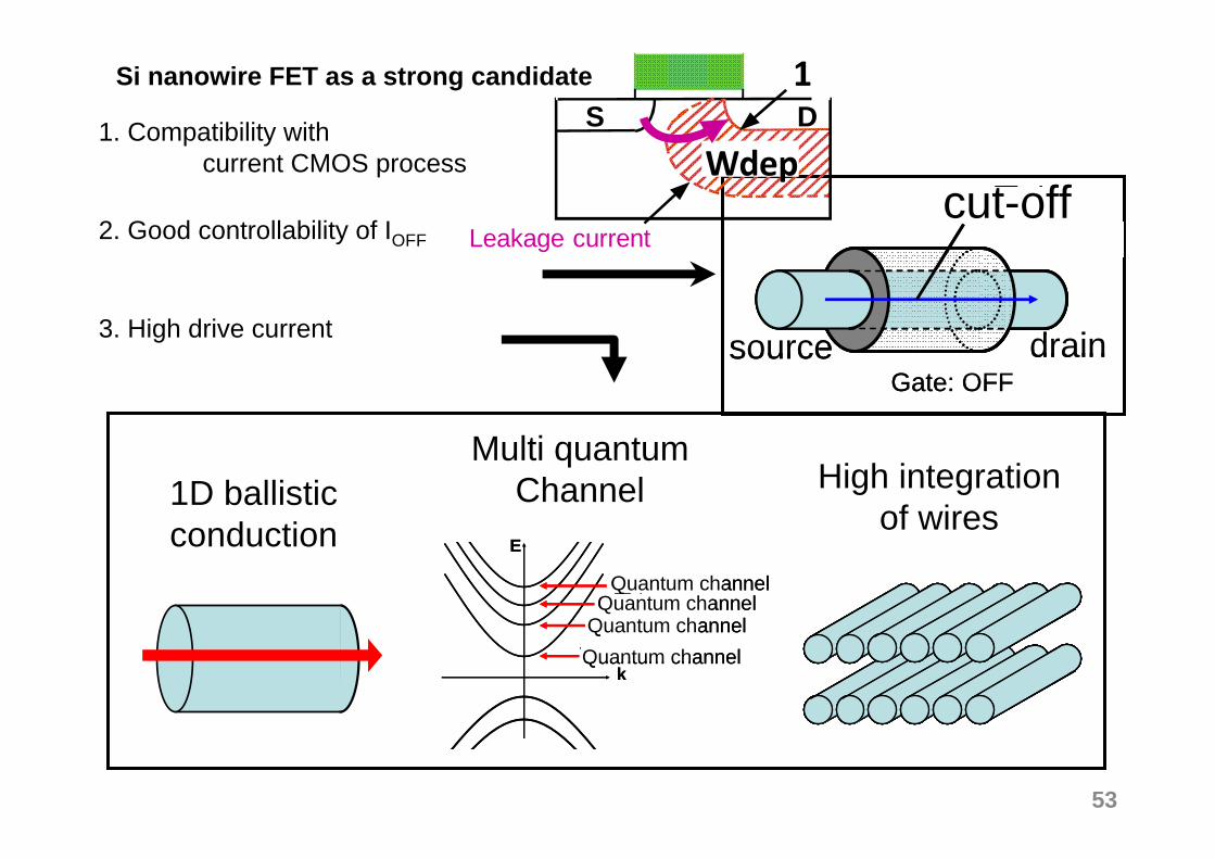
Suppression of subthreshold leakage by surrounding gate structure
Planar Surrounding gate
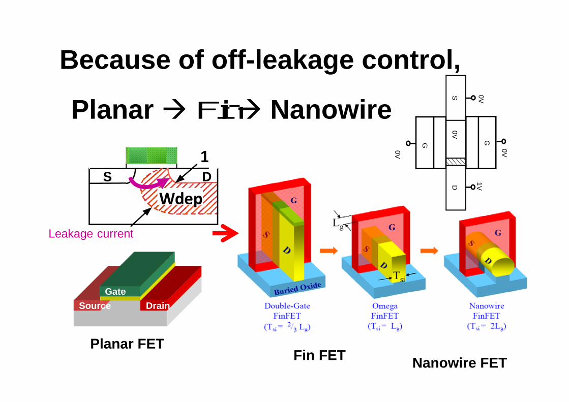
Planar Fin Nanowire
Source DrainGate
Wdep
1
Leakage current
S D
Planar FETFin FET Nanowire FET
Because of off-leakage control,1V
0V
0V0V
0VS
D
GG
52
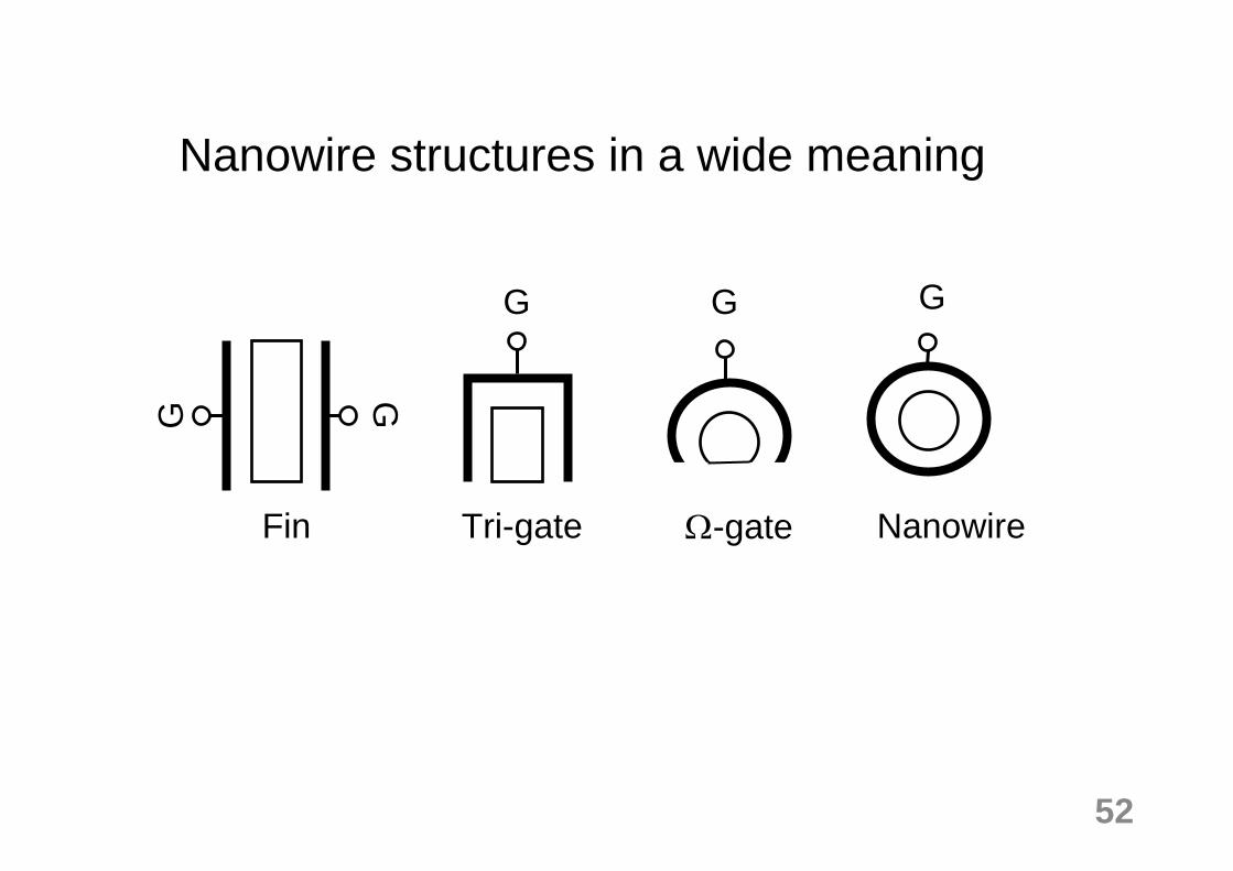
Fin Tri-gate Ω-gate Nanowire
G G G
G
GNanowire structures in a wide meaning
53
Si nanowire FET as a strong candidate
1. Compatibility with current CMOS process
2. Good controllability of IOFF
3. High drive current
1D ballisticconduction
Multi quantumChannel High integration
of wires
k
E
量子チャネル
量子チャネル量子チャネル量子チャネル
バンド図
Quantum channelQuantum channel
Quantum channelQuantum channel
k
E
量子チャネル
量子チャネル量子チャネル量子チャネル
バンド図
Quantum channelQuantum channel
Quantum channelQuantum channel
Off電流のカットオフ
Gate:OFFDrain Source
cut-off
Gate: OFFdrainsource
Off電流のカットオフ
Gate:OFFDrain Source
cut-off
Gate: OFFdrainsource
Wdep
1
Leakage current
S D
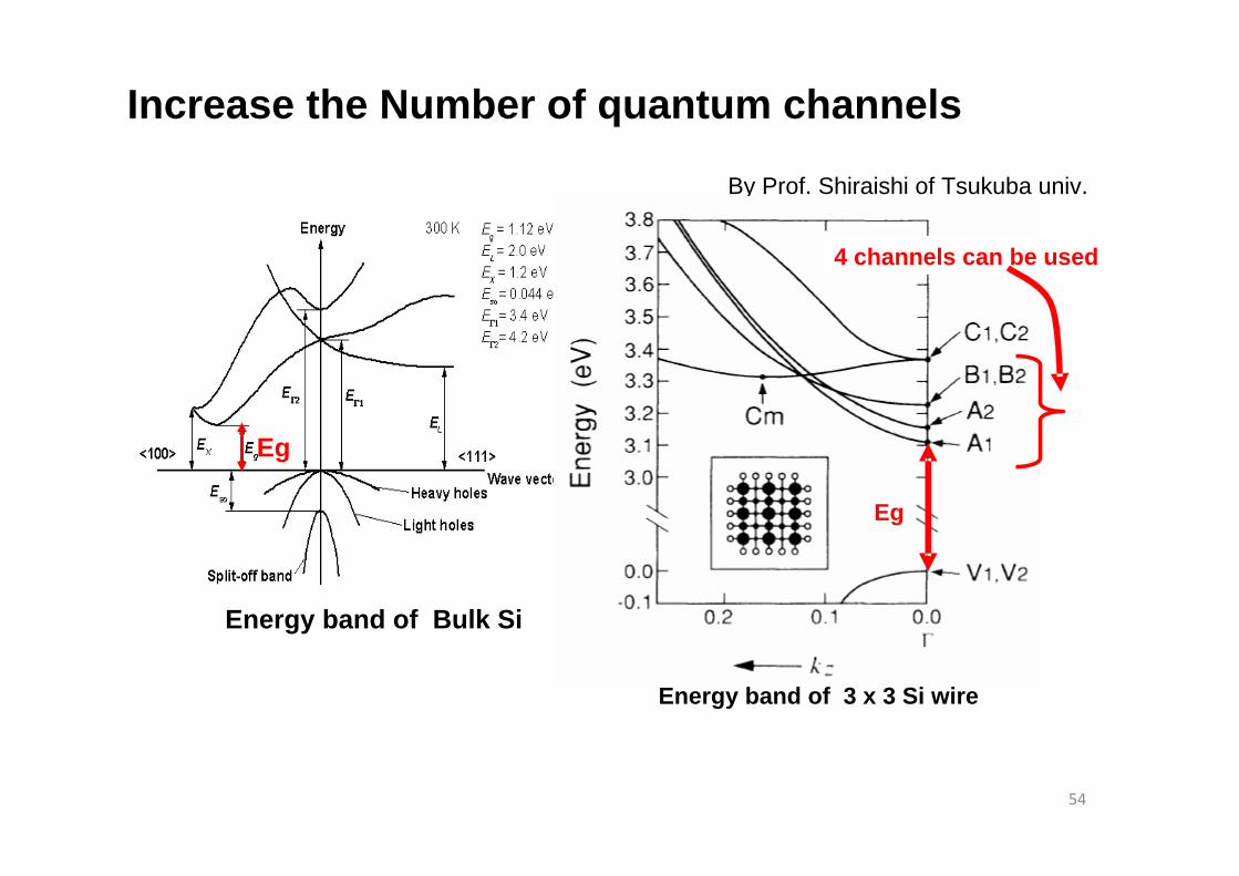
Increase the Number of quantum channels
Energy band of Bulk Si
Eg
By Prof. Shiraishi of Tsukuba univ.
Energy band of 3 x 3 Si wire
4 channels can be used
Eg
54
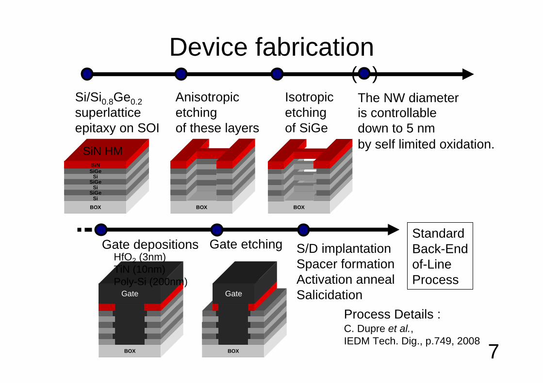
Device fabrication
Si/Si0.8Ge0.2superlatticeepitaxy on SOI
Anisotropicetchingof these layers
Isotropicetchingof SiGe
Gate depositions S/D implantationSpacer formationActivation annealSalicidation
BOXSi
SiGeSi
SiGeSi
SiGeSiN
BOX BOX
BOX
Gate
BOX
Gate
Gate etchingStandardBack-Endof-LineProcess
HfO2 (3nm)TiN (10nm)Poly-Si (200nm)
C. Dupre et al.,IEDM Tech. Dig., p.749, 2008
7
SiN HM
Process Details :
The NW diameteris controllabledown to 5 nm by self limited oxidation.
( )
Cross-section
50nm
SiN HM
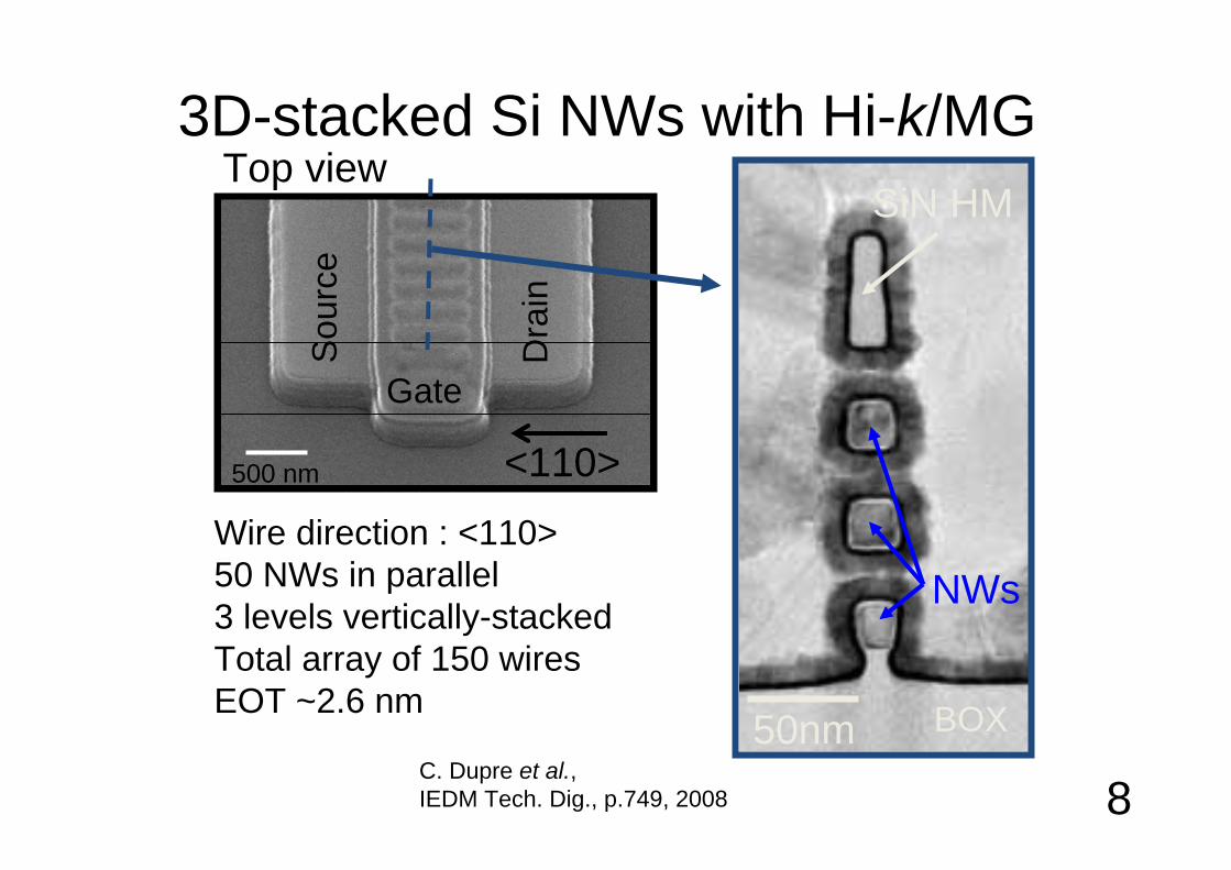
Wire direction : <110>50 NWs in parallel3 levels vertically-stackedTotal array of 150 wires EOT ~2.6 nm
NWs
8
3D-stacked Si NWs with Hi-k/MG
BOX
500 nm
Sou
rce
Dra
in
Gate
Top view
<110>
C. Dupre et al.,IEDM Tech. Dig., p.749, 2008
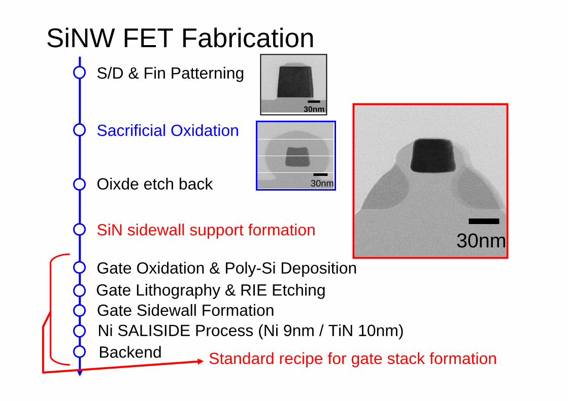
SiNW FET Fabrication
Sacrificial Oxidation
SiN sidewall support formation
Ni SALISIDE Process (Ni 9nm / TiN 10nm)
S/D & Fin Patterning
Gate Oxidation & Poly-Si DepositionGate Lithography & RIE EtchingGate Sidewall Formation
30nm
30nm
30nm
Oixde etch back
Standard recipe for gate stack formationBackend
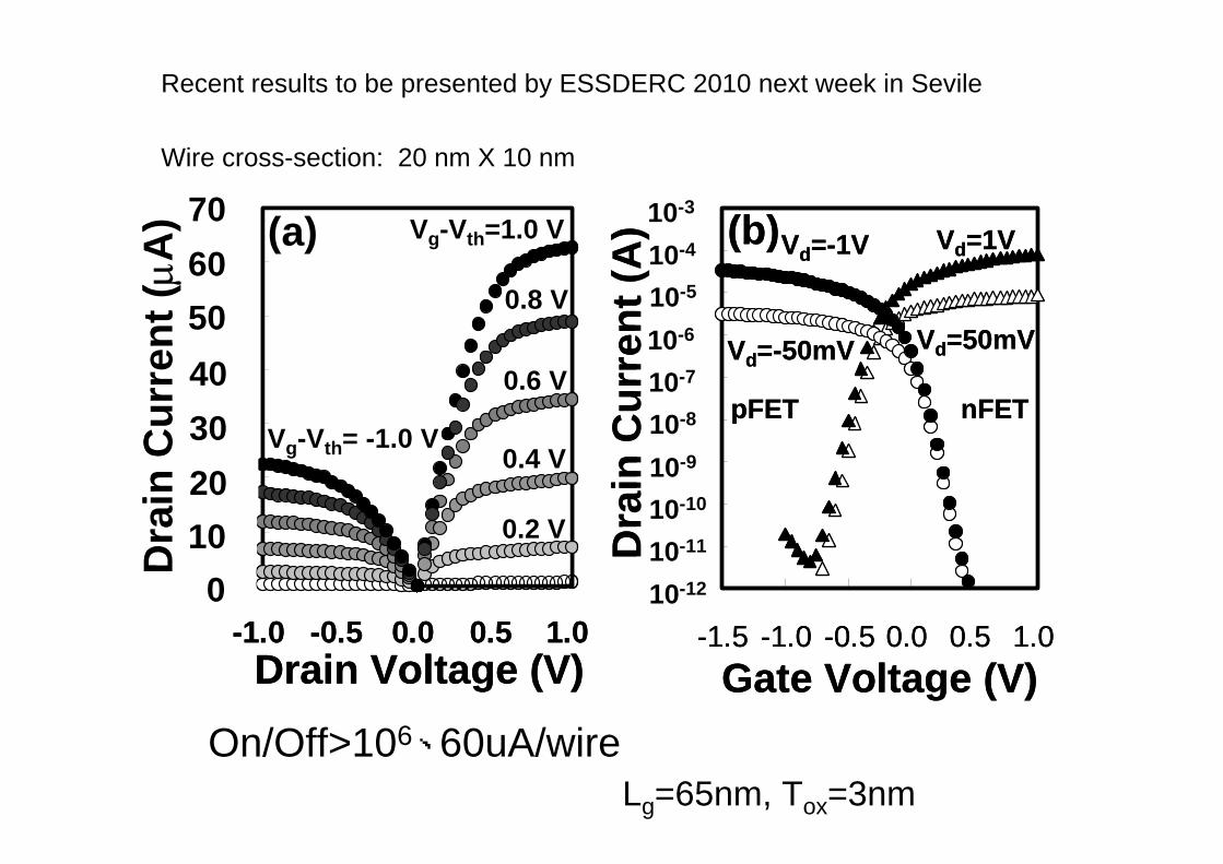
Lg=65nm, Tox=3nm
1.E-12
1.E-11
1.E-10
1.E-09
1.E-08
1.E-07
1.E-06
1.E-05
1.E-04
1.E-03
-1.5 -1.0 -0.5 0.0 0.5 1.0
0.E+00
1.E-05
2.E-05
3.E-05
4.E-05
5.E-05
6.E-05
7.E-05
-1.0 -0.5 0.0 0.5 1.00
10 20 30 40 50 60 70
Dra
in C
urre
nt (µ
A)
Drain Voltage (V)
Vg-Vth=1.0 V
Vg-Vth= -1.0 V
0.8 V
0.6 V
0.4 V
0.2 V
(a)
10-12
Gate Voltage (V)
pFET nFET
(b)
10-11
10-10
10-9
10-8
10-7
10-6
10-5
10-4
10-3
Dra
in C
urre
nt (A
)
Vd=-50mV
Vd=-1V
Vd=50mV
Vd=1V
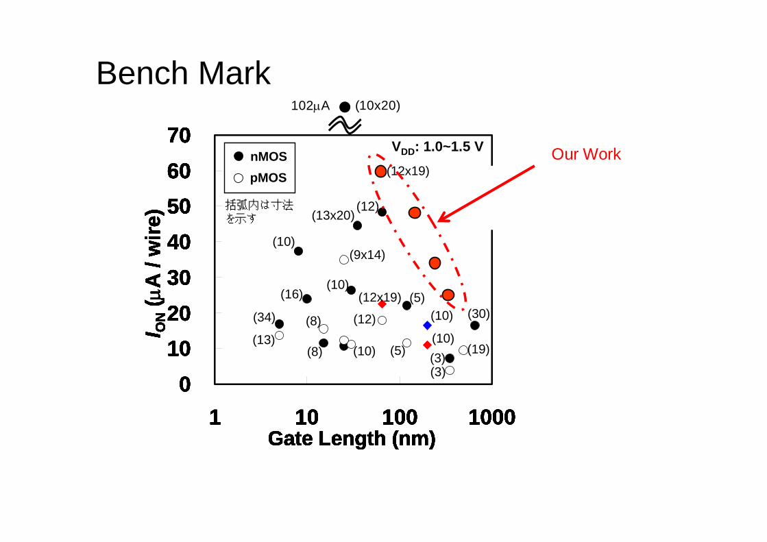
On/Off>106、60uA/wire
Recent results to be presented by ESSDERC 2010 next week in Sevile
Wire cross-section: 20 nm X 10 nm
010203040506070
1 10 100 1000Gate Length (nm)
I ON
(µA
/ w
ire)
nMOSpMOS
(5)
(5)
(10)
(10)(12)
(12x19)
(12)
(12x19)
(13x20)
(9x14)(10)
(10)
(10)
(8)
(8)
(16)
(13)
(34)
(3)(3)
(30)
(19)
VDD: 1.0~1.5 V
括弧内は寸法を示す
010203040506070
1 10 100 1000Gate Length (nm)
I ON
(µA
/ w
ire)
nMOSpMOS
010203040506070
1 10 100 1000Gate Length (nm)
I ON
(µA
/ w
ire)
nMOSpMOS
(5)
(5)
(10)
(10)(12)
(12x19)
(12)
(12x19)
(13x20)
(9x14)(10)
(10)
(10)
(8)
(8)
(16)
(13)
(34)
(3)(3)
(30)
(19)
VDD: 1.0~1.5 V
括弧内は寸法を示す
(12)
010203040506070
1 10 100 1000Gate Length (nm)
I ON
(µA
/ w
ire)
nMOSpMOS
(5)
(5)
(10)
(10)(12)
(12x19)
(12)
(12x19)
(13x20)
(9x14)(10)
(10)
(10)
(8)
(8)
(16)
(13)
(34)
(3)(3)
(30)
(19)
VDD: 1.0~1.5 V
括弧内は寸法を示す
010203040506070
1 10 100 1000Gate Length (nm)
I ON
(µA
/ w
ire)
nMOSpMOS
010203040506070
1 10 100 1000Gate Length (nm)
I ON
(µA
/ w
ire)
nMOSpMOS
(5)
(5)
(10)
(10)(12)
(12x19)
(12)
(12x19)
(13x20)
(9x14)(10)
(10)
(10)
(8)
(8)
(16)
(13)
(34)
(3)(3)
(30)
(19)
VDD: 1.0~1.5 V
括弧内は寸法を示す
010203040506070
1 10 100 1000Gate Length (nm)
I ON
(µA
/ w
ire)
nMOSpMOS
(5)
(5)
(10)
(10)(12)
(12x19)
(12)
(12x19)
(13x20)
(9x14)(10)
(10)
(10)
(8)
(8)
(16)
(13)
(34)
(3)(3)
(30)
(19)
VDD: 1.0~1.5 V
括弧内は寸法を示す
010203040506070
1 10 100 1000Gate Length (nm)
I ON
(µA
/ w
ire)
nMOSpMOS
010203040506070
1 10 100 1000Gate Length (nm)
I ON
(µA
/ w
ire)
nMOSpMOS
(5)
(5)
(10)
(10)(12)
(12x19)
(12)
(12x19)
(13x20)
(9x14)(10)
(10)
(10)
(8)
(8)
(16)
(13)
(34)
(3)(3)
(30)
(19)
VDD: 1.0~1.5 V
括弧内は寸法を示す
(12)
本研究で得られたオン電流
(10x20)102µA
Our Work
Bench Mark
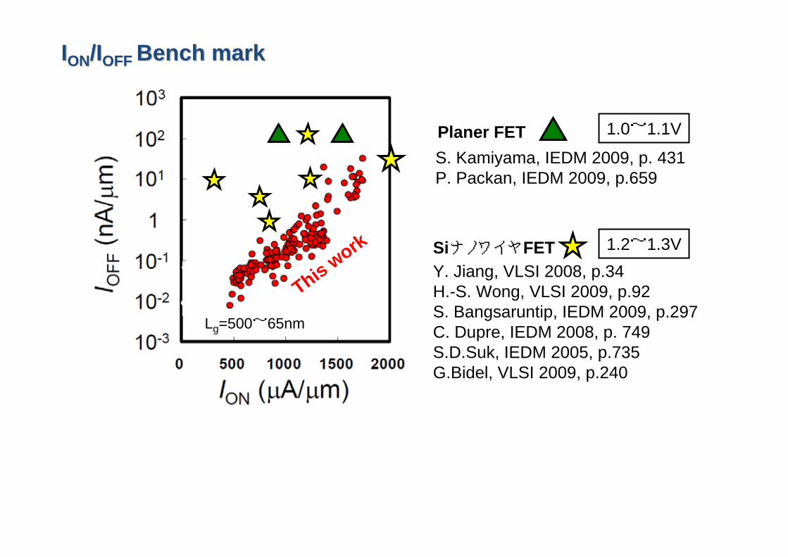
Y. Jiang, VLSI 2008, p.34H.-S. Wong, VLSI 2009, p.92S. Bangsaruntip, IEDM 2009, p.297C. Dupre, IEDM 2008, p. 749S.D.Suk, IEDM 2005, p.735G.Bidel, VLSI 2009, p.240
SiナノワイヤFET
Planer FETS. Kamiyama, IEDM 2009, p. 431P. Packan, IEDM 2009, p.659
1.2~1.3V
1.0~1.1V
Lg=500~65nm
IIONON/I/IOFF OFF Bench markBench mark
This work
0 .E + 0 0
1 .E + 1 9
2 .E + 1 9
3 .E + 1 9
4 .E + 1 9
5 .E + 1 9
6 .E + 1 9
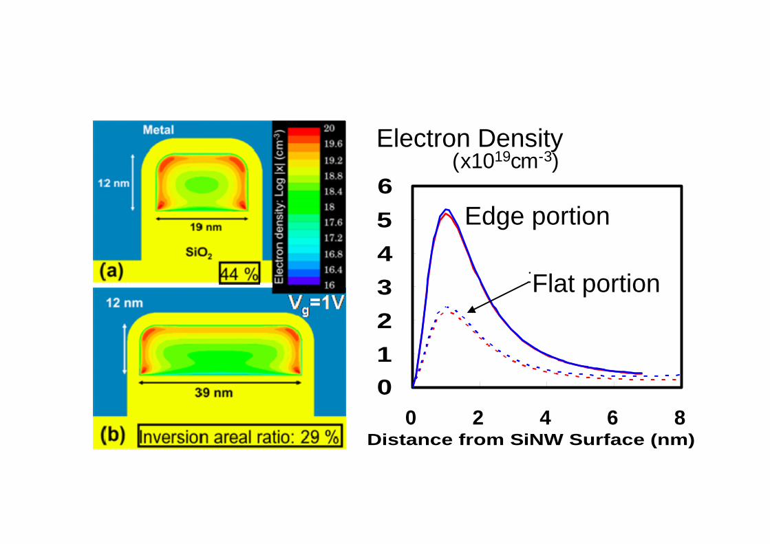
0 2 4 6 8Distance from SiNW Surface (nm)
6543210
角の部分
平らな部分
電子濃度(x1019cm-3)Electron Density
Edge portion
Flat portion
0
2000
4000
6000
8000
10000
12000
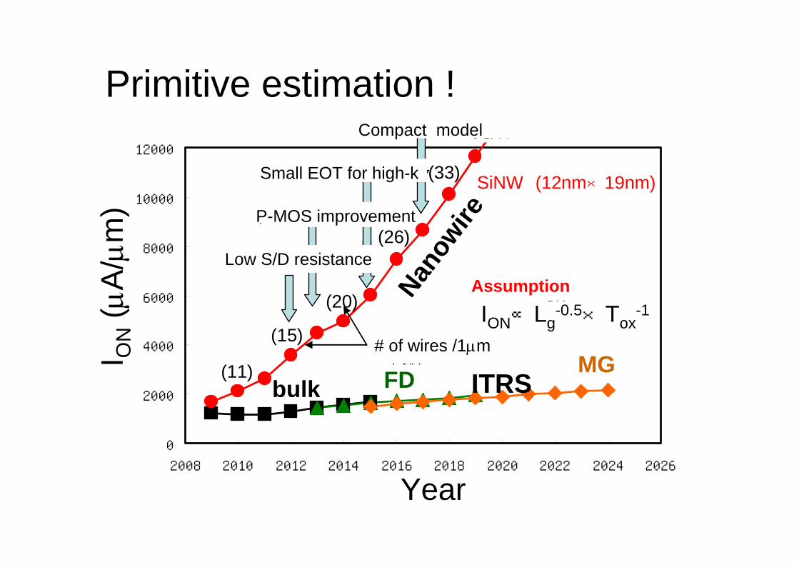
2008 2010 2012 2014 2016 2018 2020 2022 2024 2026
Year
I ON
(µA/µm
)
SiNW (12nm×19nm)
MGFDbulk
ION∝Lg-0.5×Tox
-1(20)
(11)
(33)
(15)
(26)
今回用いたIONの仮定
1µm当たりの本数
コンパクトモデルの完成
S/D寄生抵抗低減技術
pMOSの高性能化
低EOT実現技術
Compact model
Small EOT for high-k
P-MOS improvement
Low S/D resistance
# of wires /1µm
Assumption
ITRSNan
owire
Primitive estimation !
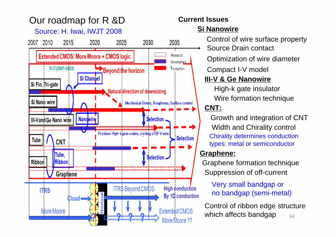
Our roadmap for R &D Source: H. Iwai, IWJT 2008
Current Issues
III-V & Ge NanowireHigh-k gate insulatorWire formation technique
CNT:
Width and Chirality control Growth and integration of CNT
Graphene:Graphene formation technique Suppression of off-current
Very small bandgap or no bandgap (semi-metal)
Control of ribbon edge structure which affects bandgap
Chirality determines conduction types: metal or semiconductor
64
Si NanowireControl of wire surface property
Compact I-V model
Source Drain contactOptimization of wire diameter

Thank you for your attention!
65