max6821/max6825 low-voltage sot23 µp … boxes computers and con- trollers embedded controllers...
TRANSCRIPT
Set-Top Boxes Computers and Con-
trollers Embedded Controllers
Intelligent Instruments Critical µP Monitoring Portable/Battery-
Powered Equipment
General DescriptionThe MAX6821–MAX6825 are low-voltage microproces-sor (µP) supervisory circuits that combine voltage mon-itoring, watchdog timer, and manual reset input func-tions in a 5-pin SOT23 package. Microprocessor super-visory circuits significantly improve system reliability and accuracy compared to separate ICs or discrete compo-nents. These devices assert a reset signal whenever the monitored voltage drops below its preset threshold, keep-ing it asserted for a minimum timeout period after VCC rises above the threshold. In addition, a watchdog timer monitors against code execution errors. A debounced manual reset is also available. The MAX6821–MAX6825 monitor voltag-es from +1.8V to +5.0V. These outputs are guaranteed to be in the correct state for VCC down to +1.0V.Nine preprogrammed reset threshold voltages are available (see the Threshold Suffix Guide). The MAX6821, MAX6822, and MAX6823 all have a manual reset input and a watchdog timer. The MAX6821 has push-pull RESET, the MAX6822 has open-drain RESET, and the MAX6823 has push-pull RESET. The MAX6824 has a watchdog timer and both push-pull RESET and push-pull RESET. The MAX6825 has a manual reset input and both push-pull RESET and push-pull RESET. The Selector Guide explains the functions offered in this series of parts.
Features Monitors +1.8V, +2.5V, +3.0V, +3.3V, +5.0V Supplies 140ms (min) Reset Timeout Delay 1.6s Watchdog Timeout Period (MAX6821/MAX6822/
MAX6823/MAX6824) Manual Reset Input (MAX6821/MAX6822/MAX6823/
MAX6825) Three Reset Output Options
Push-Pull RESET Push-Pull RESET Open-Drain RESET
Guaranteed Reset Valid to VCC = +1.0V Immune to Short Negative VCC Transients No External Components Small 5-Pin SOT23 Packages
Applications
19-1868; Rev 3; 7/14
Note: Bold indicates standard versions. Samples are typically available for standard versions only. All parts require a 2.5k minimum order increment. Contact factory for availability.
*Insert the desired suffix letter (from the table below) into the blank to complete the part number Devices are available in both leaded and lead(Pb)-free packag-ing.Specify lead-free by replacing “-T” with “+T” when ordering.
SUFFIX RESETTHRESHOLD (V)
L 4.63M 4.38T 3.08S 2.93R 2.63Z 2.32Y 2.19W 1.67V 1.58
PART* TEMP RANGE PIN-PACKAGEMAX6821_UK-T -40°C to +125°C 5 SOT23-5MAX6822_UK-T -40°C to +125°C 5 SOT23-5MAX6823_UK-T -40°C to +125°C 5 SOT23-5MAX6824_UK-T -40°C to +125°C 5 SOT23-5MAX6825_UK-T -40°C to +125°C 5 SOT23-5
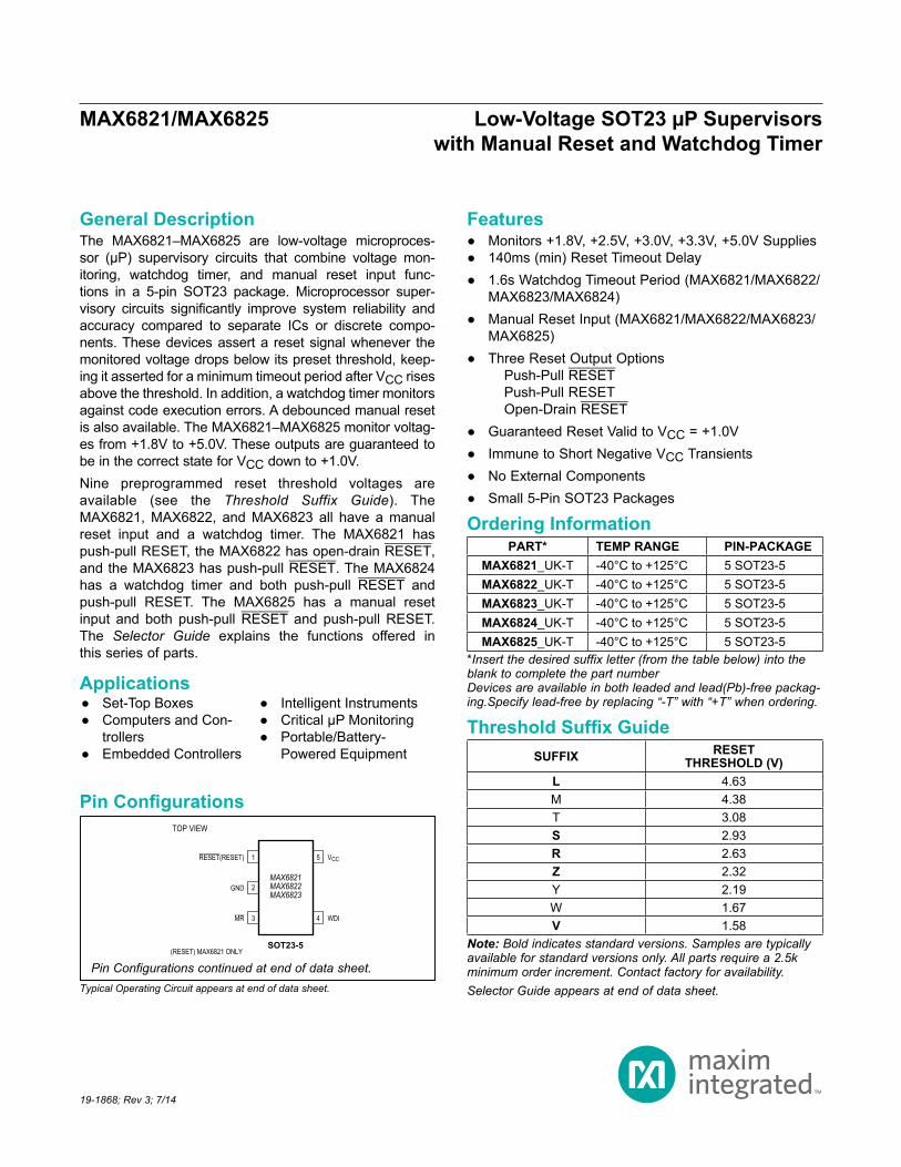
GND
WDIMR
1 5 VCCRESET(RESET)
(RESET) MAX6821 ONLY
MAX6821MAX6822MAX6823
SOT23-5
TOP VIEW
2
3 4
MAX6821/MAX6825 Low-Voltage SOT23 µP Supervisors with Manual Reset and Watchdog Timer
Selector Guide appears at end of data sheet.
Threshold Suffix Guide
Ordering Information
Typical Operating Circuit appears at end of data sheet.
Pin Configurations continued at end of data sheet.
Pin Configurations

VCC to GND .........................................................-0.3V to +6.0VOpen-Drain RESET ..............................................-0.3V to +6.0VPush-Pull RESET, RESET, MR, WDI ....... -0.3V to (VCC + 0.3V)Input Current (VCC) ............................................................20mAOutput Current (RESET, RESET) ......................................20mAContinuous Power Dissipation (TA = +70°C) 5-Pin SOT23 (derate 7.1mW/°C above +70°C) ..........571mW
Operating Temperature Range ......................... -40°C to +125°CJunction Temperature ......................................................+150°CStorage Temperature Range ............................ -65°C to +150°CLead Temperature (soldering, 10s) .................................+300°C
(VCC = +4.5V to +5.5V for MAX682_L/M, VCC = +2.7V to +3.6V for MAX682_T/S/R, VCC = +2.1V to +2.75V for MAX682_Z/Y, VCC = +1.53V to +2.0V for MAX682_W/V, TA = -40°C to +125°C, unless otherwise specified. Typical values are at TA = +25°C.) (Note 1)
PARAMETER SYMBOL CONDITIONS MIN TYP MAX UNITS
Operating Voltage Range VCCTA = 0°C to +85°C 1.0 5.5
VTA = -40°C to +125°C 1.2 5.5
VCC Supply Current(MR and WDI Unconnected) ICC
VCC = +5.5V, no loadTA = -40°C to +85°C 10 20
µA
TA = -40°C to +125°C 30
VCC = +3.6V, no loadTA = -40°C to +85°C 7 16
TA = -40°C to +125°C 25
VCC = +3.6V, no load(MAX6825 only)
TA = -40°C to +85°C 5 12
TA = -40°C to +125°C 20
VCC Reset Threshold(VCC Falling) VTH
MAX682_L TA = -40°C to +85°C 4.50 4.63 4.75
V
TA = -40°C to +125°C 4.47 4.63 4.78
MAX682_M TA = -40°C to +85°C 4.25 4.38 4.50
TA = -40°C to +125°C 4.22 4.38 4.53
MAX682_T TA = -40°C to +85°C 3.00 3.08 3.15
TA = -40°C to +125°C 2.97 3.08 3.17
MAX682_STA = -40°C to +85°C 2.85 2.93 3.00
TA = -40°C to +125°C 2.83 2.93 3.02
MAX682_R TA = -40°C to +85°C 2.55 2.63 2.70
TA = -40°C to +125°C 2.53 2.63 2.72
MAX682_Z TA = -40°C to +85°C 2.25 2.32 2.38
TA = -40°C to +125°C 2.24 2.32 2.40
MAX682_Y TA = -40°C to +85°C 2.12 2.19 2.25
TA = -40°C to +125°C 2.11 2.19 2.27
MAX682_W TA = -40°C to +85°C 1.62 1.67 1.71
TA = -40°C to +125°C 1.61 1.67 1.72
MAX682_V TA = -40°C to +85°C 1.52 1.58 1.62
Reset Threshold Temperature Coefficient 60 ppm/°C
Reset Threshold Hysteresis 2 × VTH mVVCC to Reset Output Delay tRD VCC = VTH to (VTH - 100mV) 20 µs
www.maximintegrated.com Maxim Integrated 2
MAX6821/MAX6825 Low-Voltage SOT23 µP Supervisors with Manual Reset and Watchdog Timer
Electrical Characteristics
Stresses beyond those listed under “Absolute Maximum Ratings” may cause permanent damage to the device. These are stress ratings only, and functional operation of the device at these or any other conditions beyond those indicated in the operational sections of the specifications is not implied. Exposure to absolute maximum rating conditions for extended periods may affect device reliability.
Absolute Maximum Ratings

Note 1: Over-temperature limits are guaranteed by design and not production tested. Devices tested at TA = +25°C.Note 2: Guaranteed by design and not production tested.
(VCC = +4.5V to +5.5V for MAX682_L/M, VCC = +2.7V to +3.6V for MAX682_T/S/R, VCC = +2.1V to +2.75V for MAX682_Z/Y, VCC = +1.53V to +2.0V for MAX682_W/V, TA = -40°C to +125°C, unless otherwise specified. Typical values are at TA = +25°C.) (Note 1)
PARAMETER SYMBOL CONDITIONS MIN TYP MAX UNITS
Reset Timeout Period tRPTA = -40°C to +85°C 140 200 280
msTA = -40°C to +125°C 100 320
RESET Output LOW(Push-Pull or Open-Drain) VOL
VCC ≥ 1.0V, ISINK = 50µA, reset asserted,TA = 0°C to +85°C 0.3
VVCC ≥ 1.2V, ISINK = 100µA, reset asserted 0.3
VCC ≥ 2.55V, ISINK = 1.2mA, reset asserted 0.3
VCC ≥ 4.25V, ISINK = 3.2mA, reset asserted 0.4
RESET Output HIGH(Push-Pull Only) VOH
VCC ≥ 1.8V, ISOURCE = 200µA, reset notasserted 0.8 × VCC
VVCC ≥ 3.15V, ISOURCE = 500µA, reset notasserted 0.8 × VCC
VCC ≥ 4.75V, ISOURCE = 800µA, reset notasserted 0.8 × VCC
Open-Drain RESET Output Leakage Current (Note 1) ILKG VCC > VTH, RESET not asserted 1.0 µA
RESET Output HIGH(Push-Pull Only) VOH
VCC ≥ 1.0V, ISOURCE = 1µA, reset asserted,TA = 0°C to +85°C
0.8 × VCC
VVCC ≥ 1.50V, ISOURCE = 100µA, reset asserted 0.8 × VCCVCC ≥ 2.55V, ISOURCE = 500µA, reset asserted 0.8 × VCCVCC ≥ 4.25V, ISOURCE = 800µA, reset asserted 0.8 × VCC
RESET Output LOW(Push-Pull Only) VOL
VCC ≥ 1.8V, ISINK = 500µA, reset not asserted 0.3VVCC ≥ 3.15V, ISINK = 1.2mA, reset not asserted 0.3
VCC ≥ 4.75V, ISINK = 3.2mA, reset not asserted 0.4MANUAL RESET INPUT (MAX6821/MAX6822/MAX6823/MAX6825)
MR Input VoltageVIL 0.3 × VCC VVIH 0.7 × VCC
MR Minimum Input Pulse 1 µsMR Glitch Rejection 100 nsMR to Reset Delay 200 nsMR Pullup Resistance 25 50 75 kΩWATCHDOG INPUT (MAX6821/MAX6822/MAX6823/MAX6824)
Watchdog Timeout Period tWDTA = -40°C to +85°C 1.12 1.60 2.40
sTA = -40°C to +125°C 0.80 2.60
WDI Pulse Width (Note 2) tWDI 50 ns
WDI Input VoltageVIL 0.3 × VCC VVIH 0.7 × VCC
WDI Input Current IWDIWDI = VCC, time average 120 160
µAWDI = 0, time average -20 -15
www.maximintegrated.com Maxim Integrated 3
MAX6821/MAX6825 Low-Voltage SOT23 µP Supervisors with Manual Reset and Watchdog Timer
Electrical Characteristics (continued)

(TA = +25°C, unless otherwise noted.)
2.74
2.78
2.76
2.82
2.80
2.84
2.86
2.90
2.88
2.92
0 0.1 0.2 0.3 0.4 0.5 0.6 0.7 0.8 0.9 1.0
VOLTAGE OUTPUT HIGH vs. SOURCE CURRENT
MAX
6821
toc0
8
ISOURCE (mA)
V OUT
(V)
VCC = +2.9V
0
0.10
0.05
0.20
0.15
0.30
0.25
0.35
0 2 31 4 5 6 7
VOLTAGE OUTPUT LOW vs. SINK CURRENT
MAX
6821
toc0
7
ISINK (mA)
V OUT
(V)
VCC = +2.9V
0
60
40
20
80
100
120
0 806020 40 100 120 140 160 180 200
MAXIMUM VCC TRANSIENT DURATIONvs. RESET THRESHOLD OVERDRIVE
MAX
6821
toc0
6
RESET THRESHOLD OVERDRIVE (mV), VTH - VCC
TRAN
SIEN
T DU
RATI
ON (µ
s)
RESET OCCURSABOVE CURVE
0.94
0.96
1.00
0.98
1.04
1.02
1.06
-40 0 20-20 40 60 80 100 120
NORMALIZED RESET THRESHOLDDELAY vs. TEMPERATURE
MAX
6821
toc0
5
TEMPERATURE (°C)
RESE
T TH
RESH
OLD
(V)
1.0
1.2
1.1
1.4
1.3
1.6
1.5
1.7
1.9
1.8
2.0
-40 0 20 40-20 60 80 100 120
WATCHDOG TIMEOUT PERIODvs. TEMPERATURE
MAX
6821
toc0
4
TEMPERATURE (°C)
WAT
CHDO
G TI
MEOU
T PE
RIOD
(s)
0
10
5
20
15
30
25
35
-40 0 20-20 40 60 80 100 120
VCC TO RESET OUTPUT DELAYvs. TEMPERATURE
MAX
6821
toc0
3
TEMPERATURE (°C)
PROP
AGAT
ION
DELA
Y (µ
s)
VCC FALLING, VCC = VTH - 100mV
TEMPERATURE (°C)
150
170
160
190
180
210
200
220
240
230
250
-40 0 20 40-20 60 80 100 120
RESET TIMEOUT PERIOD vs. TEMPERATURE
MAX
6821
toc0
2
RESE
T TI
MEOU
T PE
RIOD
(ms)
3
5
4
7
6
9
8
10
12
11
13
-40 0 20 40-20 60 80 100 120
SUPPLY CURRENT vs. TEMPERATURE
MAX
6821
toc0
1
TEMPERATURE (°C)
SUPP
LY C
URRE
NT (µ
A)
VCC = +5V, L VERSION
VCC = +3.3V, S VERSION
VCC = +1.8V, V VERSION
Maxim Integrated 4www.maximintegrated.com
MAX6821/MAX6825 Low-Voltage SOT23 µP Supervisors with Manual Reset and Watchdog Timer
Typical Operating Characteristics

Detailed DescriptionRESET/RESET OutputA µP’s reset input starts the µP in a known state. The MAX6821–MAX6825 µP supervisory circuits assert a reset to prevent code-execution errors during power-up, power-down, and brownout conditions. Whenever VCC falls below the reset threshold, the reset output asserts low for RESET and high for RESET. Once VCC exceeds the reset threshold, an internal timer keeps the reset out-put asserted for the specified reset timeout period (tRP); after this interval, reset output returns to its original state (see Figure 2).
Manual Reset InputMany µP-based products require manual reset capabili- ty, allowing the operator, a test technician, or external logic circuitry to initiate a reset. On the MAX6821/MAX6822/MAX6823/MAX6825, a logic low on MR asserts a reset. Reset remains asserted while MR is low, and for the timeout period (140ms min) after it
returns high. MR has an internal 50kΩ pullup resistor, so it can be left open if not used. This input can be dri-ven with CMOS logic levels or with open-drain/collector outputs. Connect a normally open momentary switch from MR to GND to create a manual reset function; external debounce circuitry is not required. If MR is dri-ven from long cables or the device is used in a noisy environment, connect a 0.1µF capacitor from MR to GND to provide additional noise immunity.
Watchdog InputIn the MAX6821–MAX6824, the watchdog circuit moni-tors the µP’s activity. If the µP does not toggle (low to high or high to low) the watchdog input (WDI) within the watchdog timeout period (1.6s nominal), reset asserts for the reset timoeout period. The internal 1.6s timer can be cleared by either a reset pulse or by toggling WDI. The WDI can detect pulses as short as 50ns. While reset is asserted, the timer remains cleared and does not count. As soon as reset is released, the timer starts counting (see Figure 3).
PIN NUMBERS PIN NAME FUNCTION
MAX6821 MAX6822 MAX6823 MAX6824 MAX6825
1 1 1 1 RESET
Active-Low Open-Drain or Push-Pull Reset Output. RESET changes from high to low when the VCC input drops below the selected reset threshold, MR is pulled low, or the watchdog triggers a reset. RESET remains low for the reset timeout period after VCC exceeds the device reset threshold, MR goes low to high, or the watchdog triggers a reset.
1 3 3 RESET
Active-High Push-Pull Reset Output. RESET changes from low to high when the VCC input drops below the selected reset threshold, MR is pulled low, or the watchdog triggers a reset. RESET remains high for the reset timeout period after VCC exceeds the device reset threshold, MR goes low to high, or the watchdog triggers a reset.
2 2 2 2 2 GND Ground
3 3 3 4 MRActive-Low Manual Reset Input. Internal 50kΩ pullup to VCC. Pull low to force a reset. Reset remains active as long as MR is low and for the reset timeout period after MR goes high. Leave unconnected or connect to VCC if unused.
4 4 4 4 WDI
Watchdog Input. If WDI remains high or low for longer than the watchdog timeout period, the internal watchdog timer runs out and a reset is triggered for the reset timeout period. The internal watchdog timer clears whenever reset is asserted, the manual reset is asserted, or WDI sees a rising or falling edge. If WDI is left unconnected or is connected to a three-stated buffer output, the watchdog feature is disabled.
5 5 5 5 5 VCC Supply Voltage and Input for Reset Threshold Monitor
www.maximintegrated.com Maxim Integrated 5
MAX6821/MAX6825 Low-Voltage SOT23 µP Supervisors with Manual Reset and Watchdog Timer
Pin Description

Disable the watchdog function by leaving WDI uncon-nected or by three-stating the driver connected to WDI. The watchdog input is internally driven low during the first 7/8 of the watchdog timeout period and high for the last 1/8 of the watchdog timeout period. When WDI is left unconnected, this internal driver clears the 1.6s timer every 1.4s. When WDI is three-stated or unconnected, the maximum allowable leakage current is 10µA and the maximum allowable load capacitance is 200pF.
Applications InformationWatchdog Input CurrentThe MAX6821/MAX6822/MAX6823/MAX6824 WDI inputs are internally driven through a buffer and series resistor from the watchdog timer (Figure 1). When WDI is left unconnected, the watchdog timer is serviced within the watchdog timeout period by a low-high-low pulse from the counter chain. For minimum watchdog input current (minimum overall power consumption), leave WDI low for the majority of the watchdog timeout period, pulsing it low-high-low once within the first 7/8 of the watchdog timeout period to reset the watchdog timer. If WDI is externally driven high for the majority of the timeout period, up to 160µA can flow into WDI.
Interfacing to µPs with Bidirectional Reset PinsSince the RESET output on the MAX6822 is open drain, it interfaces easily with µPs that have bidirectional reset pins, such as the Motorola 68HC11. Connecting the µP supervisor’s RESET output directly to the microcon- troller’s RESET pin with a single pullup resistor allows either device to assert reset (see Figure 4).
Negative-Going VCC TransientsThese supervisors are relatively immune to short-dura-tion, negative-going VCC transients (glitches), which usually do not require the entire system to shut down.
Figure 2. Reset Timing Diagram
Figure 1. Functional Diagram
VCC
1V1V
tRD
VTH VTH
tRDRESETGND
RESET
tRP
tRP
MAX6821–MAX6825
VCC
VCC
WDI(MAX6821–MAX6824)
1.26V
GND
RESET(MAX6821/MAX6824/ MAX6825)
RESET (MAX6822–MAX6825)
MR(MAX6821–MAX6823,
MAX6825)
RESETGENERATOR
WATCHDOGTIMER
WATCHDOGTRANSITIONDETECTOR
www.maximintegrated.com Maxim Integrated 6
MAX6821/MAX6825 Low-Voltage SOT23 µP Supervisors with Manual Reset and Watchdog Timer

Resets are issued to the µP during power-up, pow-er-down, and brownout conditions. The Typical Operating Characteristics show a graph of the MAX6821–MAX6825’s Maximum VCC Transient Duration vs. Reset Threshold Overdrive, for which reset pulses are not generated. The graph was produced using negative-going VCC pulses, starting at the standard monitored voltage and ending below the reset threshold by the magnitude indicated (reset threshold overdrive). The graph shows the max-imum pulse width that a negative-going VCC transient can typically have without triggering a reset pulse. As the amplitude of the transient increases (i.e., goes farther below the reset threshold), the maximum allowable pulse width decreases. Typically, a VCC transient that goes 100mV below the reset threshold and lasts for 20µs or less will not trigger a reset pulse.
Watchdog Software ConsiderationsOne way to help the watchdog timer monitor software execution more closely is to set and reset the watchdog input at different points in the program, rather than pulsing the watchdog input high-low-high or low-high-low. This technique avoids a stuck loop, in which the watchdog timer would continue to be reset inside the loop, keeping the watchdog from timing out.Figure 5 shows an example of a flow diagram where the I/O driving the watchdog input is set high at the begin-ning of the program, set low at the beginning of every subroutine or loop, then set high again when the program returns to the beginning. If the program should hang in any subroutine, the problem would quickly be corrected, since the I/O is continually set low and the watchdog timer is allowed to time out, causing a reset or interrupt to be issued. As described in the Watchdog Input Current section, this scheme results in higher time average WDI input current than does leaving WDI low for the majority of the timeout period and periodically pulsing it low-high-low.
Figure 5. Watchdog Flow Diagram
Figure 4. Interfacing open-Drain RESET to µPs with Bidirectional Reset I/O
Figure 3. Watchdog Timing Relationship
MAX6823 µP
VCC
VCC
VCC
GNDMANUALRESET
RESET
I/O
RESET
MRWDI
START
SET WDIHIGH
PROGRAMCODE
SUBROUTINE ORPROGRAM LOOP
SET WDI LOW
RETURN
MAX6822
RESETGENERATOR
GND GND
VCC VCC
RESET RESET
µP
VCC
tWD tRPtRP
tRST
WDI
RESET*
*RESET IS THE INVERSE OF RESET.
www.maximintegrated.com Maxim Integrated 7
MAX6821/MAX6825 Low-Voltage SOT23 µP Supervisors with Manual Reset and Watchdog Timer
Typical Operating Circuit

FUNCTION ACTIVE-LOW RESET
ACTIVE-HIGH RESET
OPEN-DRAIN RESET
WATCHDOG INPUT
MANUAL RESET INPUT
MAX6821 — —
MAX6822 — —
MAX6823 — —
MAX6824 — —
MAX6825 — —
PACKAGE TYPE
PACKAGE CODE OUTLINE NO. LAND PATTERN
NO.
5 SOT23 U5-1 21-0057 —
GND
WDIRESET
1 5 VCCRESET
MAX6824
SOT23-5
TOP VIEW
2
3 4
GND
MRRESET
1 5 VCCRESET
MAX6825
SOT23-5
2
3 4
www.maximintegrated.com Maxim Integrated 8
MAX6821/MAX6825 Low-Voltage SOT23 µP Supervisors with Manual Reset and Watchdog Timer
Package InformationFor the latest package outline information and land patterns (footprints), go to www.maximintegrated.com/packages. Note that a “+”, “#”, or “-” in the package code indicates RoHS status only. Package drawings may show a different suffix character, but the drawing pertains to the package regardless of RoHS status.
Chip InformationTRANSISTOR COUNT: 750PROCESS: BiCMOS
Pin Configurations (continued)
Selector Guide
REVISION NUMBER
REVISION DATE DESCRIPTION PAGES
CHANGED
3 7/14 No /V OPNs; removed automotive reference from Applications section 1
Maxim Integrated cannot assume responsibility for use of any circuitry other than circuitry entirely embodied in a Maxim Integrated product. No circuit patent licenses are implied. Maxim Integrated reserves the right to change the circuitry and specifications without notice at any time. The parametric values (min and max limits) shown in the Electrical Characteristics table are guaranteed. Other parametric values quoted in this data sheet are provided for guidance.
Maxim Integrated and the Maxim Integrated logo are trademarks of Maxim Integrated Products, Inc. © 2014 Maxim Integrated Products, Inc. 9
MAX6821/MAX6825 Low-Voltage SOT23 µP Supervisors with Manual Reset and Watchdog Timer
Revision History
For pricing, delivery, and ordering information, please contact Maxim Direct at 1-888-629-4642, or visit Maxim Integrated’s website at www.maximintegrated.com.