memory bist tutorial
TRANSCRIPT


Fault modelsFault models
Stuck-at-0Stuck-at-0
0000
1111 Stuck-at-1Stuck-at-1
Reset coupling Reset coupling 00 00 Set coupling Set coupling1111
0000
1111 1111
Inversion coupling Inversion coupling 00 111111
0000
Transition Transition /0 /0 00 11 Transition Transition /1/1
ADRADRADRADR
00 00 Inversion coupling Inversion coupling1111 1111
0000
1111
AND bridging AND bridging 00 110000 0000
11 00 OR bridging OR bridging1111 1111
NeighborhoodNeighborhoodpattern sensitivepattern sensitive
faults (active)faults (active)
0000
1111 0000 1111
1111
00001111
NeighborhoodNeighborhoodpattern sensitivepattern sensitivefaults (passive)faults (passive)
1111
1111 11110000
0000
0000
Address decoderAddress decoderfaultsfaults ADRADRADRADR ADRADRADRADR ADRADRADRADR ADRADRADRADR
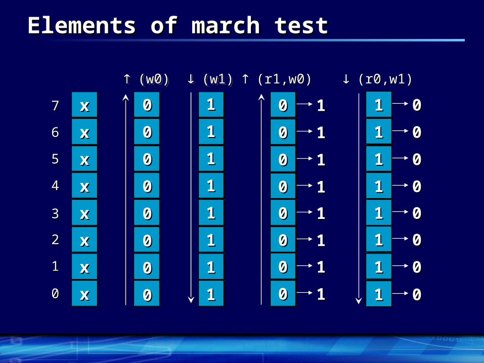
Elements of march testElements of march test
(w0)(w0) (w0)(w0)
xxxx
xxxx
xxxx
xxxx
xxxx
xxxx
xxxx
xxxx
77
66
55
44
33
22
11
00
00
(r1,w0)(r1,w0)
1 1 1 1
1111
1 1 1 1
1 1 1 1
1 1 1 1
1 1 1 1
1 1 1 1
1111
(w1)(w1) (w1)(w1)
(r0,w1)(r0,w1)
0000
0 0 0 0
0 0 0 0
0 0 0 0
0000
0 0 0 0
0000
0000
00
00
00
00
00
00
00
11
11
11
11
11
11
11
11
0000 11
0000 11
0000 11
0000 11
0000 11
0000 11
0000 11
0000 11
1111 00
1111 00
1111 00
1111 00
1111 00
1111 00
1111 00
1111 00

C - algorithmC - algorithm
Number of steps: 10n Fault coverage: AFs, SAFs, TFs, CFins , CFids
(w0)(w0)
(r1,w0)(r1,w0)
1 1 1 1
1111
1 1 1 1
1 1 1 1
1 1 1 1
1 1 1 1
1 1 1 1
1111
(r0,w1)(r0,w1)
0000
0 0 0 0
0 0 0 0
0 0 0 0
0000
0 0 0 0
0000
0000
00
00
00
00
00
00
00
00
0000 11
0000 11
0000 11
0000 11
0000 11
0000 11
0000 11
0000 11
1111 00
1111 00
1111 00
1111 00
1111 00
1111 00
1111 00
1111 00
(r0,w1)(r0,w1) (r0,w1)(r0,w1)
0000
0 0 0 0
0 0 0 0
0 0 0 0
0000
0 0 0 0
0000
0000
1111 00
1111 00
1111 00
1111 00
1111 00
1111 00
1111 00
1111 00
(r1,w0)(r1,w0)
1 1 1 1
1111
1 1 1 1
1 1 1 1
1 1 1 1
1 1 1 1
1 1 1 1
1111
0000 11
0000 11
0000 11
0000 11
0000 11
0000 11
0000 11
0000 11
(r0)(r0)
00
00
00
00
00
00
00
00
0000
0000
0000
0000
0000
0000
0000
0000
00
00
00
00
00
00
00
00

Checkerboard test and data retentionCheckerboard test and data retention
Designed to test refresh Designed to test refresh operations of DRAMsoperations of DRAMs
Maximizes leakage current Maximizes leakage current and detects leakage faultsand detects leakage faults
Used as data retention testUsed as data retention test To be effective it must To be effective it must
consider address consider address scrambling and layoutscrambling and layout
1111 0000 1111 0000
0000 1111 0000 1111
0000 1111 0000 1111
1111 0000 1111 0000

Data backgrounds for word memoriesData backgrounds for word memories Multiple data backgrounds to detect coupling and bridging faults between cells of the same word For every pair of cells all four combinations are checked 2 (log2w + 1) backgrounds 16 backgrounds for
128-bit wide memory Normal and inverse
Multiple data backgrounds to detect coupling and bridging faults between cells of the same word For every pair of cells all four combinations are checked 2 (log2w + 1) backgrounds 16 backgrounds for
128-bit wide memory Normal and inverse
D0D0 D1D1 D2D2 D3D3 D4D4 D5D5 D6D6 D7D7
00 0 0 0 0 0 0 0 0 0 0 0 0 0 0 11 1 1 1 1 1 1 1 1 1 1 1 1 1 1 00 0 0 0 0 0 0 1 1 1 1 1 1 1 1 11 1 1 1 1 1 1 0 0 0 0 0 0 0 0 00 0 0 1 1 1 1 0 0 0 0 1 1 1 1 11 1 1 0 0 0 0 1 1 1 1 0 0 0 0 00 1 1 0 0 1 1 0 0 1 1 0 0 1 1 11 0 0 1 1 0 0 1 1 0 0 1 1 0 0

Data in word-oriented memoryData in word-oriented memory (w0)(w0) (r1,w0)(r1,w0) (r0,w1)(r0,w1) (r0,w1)(r0,w1)

Parallel memory BISTParallel memory BIST
BIST BIST modemode
ClockClock System logicSystem logic
Address generatorAddress generatorAddress generatorAddress generatorFFSSMM
FFSSMM
Data generatorData generatorData generatorData generator
Control generatorControl generatorControl generatorControl generator
StartStart
HoldHold
DoneDone
FailFail
MemoryMemory

Serial memory BISTSerial memory BIST
System logicSystem logic
Data outputData output
Serial outputSerial outputSerial inputSerial input
Address MAddress M00 00 00 00
r0r0 00 00 00 00w1 w1 11 00 00 00r0r0 11 00 00 00w1w1 11 11 00 00r0r0 11 11 00 00w1w1 11 11 11 00r0r0 11 11 11 00w1w1 11 11 11 11r1r1 11 11 11 11
Minimal logic and routingMinimal logic and routing Longer test timeLonger test time
MemoryMemory

Serial-parallel data interface trade-offsSerial-parallel data interface trade-offs
MemoryMemory
MemoryMemoryMemoryMemory
MemoryMemory

Memory BIST collarMemory BIST collar
++++
Memory BISTMemory BISTcontrollercontroller
Memory BISTMemory BISTcontrollercontroller
To / FromTo / FromTAP controllerTAP controller
Embedded memory BIST collarEmbedded memory BIST collar•mux address / control bus and data linesmux address / control bus and data lines•local comparator with singlelocal comparator with single pass/failpass/fail•local data generator to reduce routinglocal data generator to reduce routingarea and timing problemsarea and timing problems•local address validationlocal address validation
Memory controller at the top levelMemory controller at the top level•TAP controller as test engine TAP controller as test engine
MemoryMemoryarrayarray
Functional logicFunctional logic

Shared controller and parallel testShared controller and parallel test
Insert collarsInsert collars Connect them Connect them
through memory test through memory test busbus
• to memory BIST to memory BIST controllercontroller
• to TAPto TAP
++++
Memory BISTMemory BISTcontrollercontroller
Memory BISTMemory BISTcontrollercontroller
To / FromTo / FromTAP controllerTAP controller
MemoryMemoryarrayarray
++++
MemoryMemoryarrayarray
Functional logicFunctional logic

Parallel memory BIST collarParallel memory BIST collar
Memory arrayMemory array
Data inData inAddressAddress Data outData outCtrlCtrl
MBIST modeMBIST mode
SinSin
SoutSout
ClockClock
= ?= ?= ?= ?
Functional addressFunctional addressBIST addressBIST address
Functional dataFunctional dataBIST dataBIST data
Pass / FailPass / Fail
BIS
T c
ontr
olB
IST
con
trol
Fun
ctio
nal c
ontr
olF
unct
iona
l con
trol

Full-Speed test applicationFull-Speed test application
Runs at system clock speeds with single cycle read/write operations
Uncovers speed-related defects Reduce test application time.
Addr/Cntrl/Data
Clock
MemoryOutput
CompareCircuitry
CircuitOutput
Write
ClockCycle 1
ClockCycle 2
ClockCycle 3
ClockCycle 4
ClockCycle 5
SetupRead 1SetupRead 1
SetupWrite 1
SetupRead 2
SetupRead 3
SetupWrite 2
CompareRead 1
Write 1
•••Read 2 Read 3
CompareRead 2
Pass/FailRead 2
Pass/FailRead 1
CompareRead 3
Read 1

DiagnosticsDiagnostics
Detect failing location/data during test Should diagnose speed related defects Two types - Hold and resume, Hold and restart How it works?
• BIST controller stops after 1 (or 2) failures• Fail data is scanned out• BIST session resumes from where it stops (Hold and
resume)• BIST session restarts after fail data is scanned out
(Hold and restart)

Full-speed diagnosticsFull-speed diagnostics
++++
Memoryarray
Memoryarray
MBISTcontroller
ATERestart
Diagnostic monitor

Yield improvement with memory redundancyYield improvement with memory redundancy
Memory percentage, defect rate, and redundancy amount affect yield
Source: Zorian, Rodgers, DATE 2002
Redundancy Yield Improvement
0
10
20
30
40
50
60
70
80
90
100
0 10 20 30 40 50 60 70 80 90 100
Chip Memory Percentage
Mem
ory
Yie
ld
Optimal
Level 3Redundancy
Level 2Redundancy
Level 1Redundancy
No Redundancy

++++
Memory BISTcontroller
Memory BISTcontroller
MemoryArray
MemoryArray
Redundancy and repairRedundancy and repair
Extra columns, rows, or rows and columns
At the end of test - good, repairable, or non-repairable
Repair data scanned out at the end of test

Full-Chip memory BIST integrationFull-Chip memory BIST integration
Assign memories to controller
(BIST Scheduling)
Assign memories to controller
(BIST Scheduling)
Memory BIST Generation
(Generate Controller/Collars)
Memory BIST Generation
(Generate Controller/Collars)
BIST GENERATION
Read in SOC netlist
Identify memories
Read in SOC netlist
Identify memories
Insert controllers in the design
Stitch controllers to top-level
Insert controllers in the design
Stitch controllers to top-level
BIST INSERTION

Full Chip Memory BIST Control Full Chip Memory BIST Control
Block BIST Block
BIST Block
BIST
Controller
Memory 1 Memory 1
Memory 2 Memory 2
SOC
TDO
MBIST Data Register
TDI
CLK
TM S
TCK
TRST
TAP Controller
rst_l
test_h
test_done
fail_h
Boundary Scan Register

Programmable algorithmsProgrammable algorithms
Selection of algorithmsSelection of algorithms• March1, March2, March3, Unique Address, Checkerboard, …March1, March2, March3, Unique Address, Checkerboard, …• address jumpingaddress jumping
Synthesizable algorithmsSynthesizable algorithms• user defined prior to synthesisuser defined prior to synthesis• simple languagesimple language• number of sequences, backgrounds, sequence elements etc.,number of sequences, backgrounds, sequence elements etc.,
Programmable algorithmsProgrammable algorithms• defect mechanisms may not be known before fabricationdefect mechanisms may not be known before fabrication• memory BIST controller implements a class of algorithmsmemory BIST controller implements a class of algorithms• field programmable parameters define active elements of test
sequences

SummarySummary
Key components of a BIST controller • algorithm controller• data background generator• address generator• comparator
Very high quality test of embedded arrays BIST controller shared across a number of memory
arrays to reduce area BIST diagnostics helps in gathering failure
information Built-in repair results in yield improvement