mf1167-01 sed 1335 series lcd controller icstechnical manual
TRANSCRIPT
SED 1335 Series
LCD Controller IC
s
Technica
l Manual
MF1167-01

No part of this material may be reproduced or duplicated in any form or by any means without the written
permission of Seiko Epson. Seiko Epson reserves the right to make changes to this material without notice.Seiko Epson does not assume any liability of any kind arising out of any inaccuracies contained in this
material or due to its application or use in any product or circuit and, further, there is no representation that
this material is applicable to products requiring high level reliability, such as, medical products. Moreover,no license to any intellectual property rights is granted by implication or otherwise, and there is no represen-
tation or warranty that anything made in accordance with this material will be free from any patent or
copyright infringement of a third party. This material or portions thereof may contain technology or thesubject relating to strategic products under the control of the Foreign Exchange and Foreign Trade Control
Law of Japan and may require an export license from the Ministry of International Trade and Industry or
other approval from another government agency.
In this manual, Zilog's Z80-CPU or its equivalent shall be called Z80, Intel's 8085A or its equivalent shall
be called 8085 and Motorola's MC6809 and MC6802 or their equivalents shall be called 6809 and 6802,respectively.
® stands for registered trade mark.
All other product names mentioned herein are trademarks and/or registered trademarks of their respec-tive owners.
© Seiko Epson Corporation 1999 All rights reserved.
CONTENTS
SED1335 Series EPSON iTechnical Manual
CONTENTS
1. OVERVIEW ................................................................................................................................................................. 1
2. FEATURES ................................................................................................................................................................. 1
3. BLOCK DIAGRAM ....................................................................................................................................................... 2
4. PINOUTS ..................................................................................................................................................................... 3
5. PIN DESCRIPTION ..................................................................................................................................................... 4
5.1. SED1335F0A/0B Pin Summary ........................................................................................................................... 4
5.2. Pin Functions ..................................................................................................................................................... 55.2.1. Power supply ......................................................................................................................................... 55.2.2. Oscillator ................................................................................................................................................ 55.2.3. Microprocessor interface ........................................................................................................................ 55.2.4. Display memory control ......................................................................................................................... 65.2.5. LCD drive signals ................................................................................................................................... 7
6. SPECIFICATIONS ....................................................................................................................................................... 7
6.1. Absolute Maximum Ratings ............................................................................................................................... 7
6.2. SED1335 ............................................................................................................................................................ 8
6.3. SED1335F Timing Diagrams ........................................................................................................................... 106.3.1. 8080 family interface timing ................................................................................................................. 106.3.2. 6800 family interface timing ................................................................................................................. 116.3.3. Display memory read timing ................................................................................................................ 126.3.4. Display memory write timing ................................................................................................................ 136.3.5. SLEEP IN command timing ................................................................................................................. 156.3.6. External oscillator signal timing ............................................................................................................ 166.3.7. LCD output timing ................................................................................................................................ 17
7. PACKAGE DIMENSIONS ......................................................................................................................................... 19
7.1. SED1335F0A .......................................................................................................................................................................................... 19
7.2. SED1335F0B .......................................................................................................................................................................................... 19
8. INSTRUCTION SET .................................................................................................................................................. 20
8.1. The Command Set ........................................................................................................................................... 20
8.2. System Control Commands ............................................................................................................................. 218.2.1. SYSTEM SET ...................................................................................................................................... 21
8.2.1.1. C ........................................................................................................................................... 218.2.1.2. M0 ......................................................................................................................................... 218.2.1.3. M1 ......................................................................................................................................... 218.2.1.4. M2 ......................................................................................................................................... 228.2.1.5. W/S ....................................................................................................................................... 228.2.1.6. IV .......................................................................................................................................... 238.2.1.7. FX ......................................................................................................................................... 248.2.1.8. WF ........................................................................................................................................ 258.2.1.9. FY ......................................................................................................................................... 258.2.1.10. C/R ....................................................................................................................................... 258.2.1.11. TC/R ..................................................................................................................................... 268.2.1.12. L/F ........................................................................................................................................ 268.2.1.13. AP ......................................................................................................................................... 27
8.2.2. SLEEP IN ............................................................................................................................................. 27
8.3. Display Control Commands ............................................................................................................................. 288.3.1. DISP ON/OFF ...................................................................................................................................... 28
8.3.1.1. D ........................................................................................................................................... 288.3.1.2. FC ......................................................................................................................................... 288.3.1.3. FP ......................................................................................................................................... 28
8.3.2. SCROLL ............................................................................................................................................... 298.3.2.1. C ........................................................................................................................................... 298.3.2.2. SL1, SL2 ............................................................................................................................... 30

CONTENTS
ii EPSON SED1335 SeriesTechnical Manual
8.3.3. CSRFORM ........................................................................................................................................... 348.3.3.1. CRX ...................................................................................................................................... 348.3.3.2. CRY ...................................................................................................................................... 348.3.3.3. CM ........................................................................................................................................ 34
8.3.4. CSRDIR ............................................................................................................................................... 348.3.5. OVLAY ................................................................................................................................................. 35
8.3.5.1. MX0, MX1 ............................................................................................................................. 358.3.5.2. DM1, DM2 ............................................................................................................................ 368.3.5.3. OV ........................................................................................................................................ 36
8.3.6. CGRAM ADR ....................................................................................................................................... 368.3.7. HDOT SCR .......................................................................................................................................... 37
8.3.7.1. D0 to D2 ............................................................................................................................... 37
8.4. Drawing Control Commands ............................................................................................................................ 378.4.1. CSRW .................................................................................................................................................. 378.4.2. CSRR ................................................................................................................................................... 38
8.5. Memory Control Commands ............................................................................................................................ 388.5.1. MWRITE .............................................................................................................................................. 388.5.2 MREAD ................................................................................................................................................ 39
9. DISPLAY CONTROL FUNCTIONS ........................................................................................................................... 40
9.1. Character Configuration ................................................................................................................................... 40
9.2. Screen Configuration ....................................................................................................................................... 429.2.1. Screen configuration ............................................................................................................................ 429.2.2. Display address scanning .................................................................................................................... 429.2.3. Display scan timing .............................................................................................................................. 45
9.3. Cursor Control .................................................................................................................................................. 469.3.1. Cursor register function ........................................................................................................................ 469.3.2. Cursor movement ................................................................................................................................ 469.3.3. Cursor display layers ........................................................................................................................... 46
9.4. Memory to Display Relationship ...................................................................................................................... 48
9.5. Scrolling ........................................................................................................................................................... 519.5.1. On-page scrolling ................................................................................................................................. 519.5.2. Inter-page scrolling .............................................................................................................................. 519.5.3. Horizontal scrolling ............................................................................................................................... 529.5.4. Bidirectional scrolling ........................................................................................................................... 539.5.5. Scroll units ........................................................................................................................................... 53
10. CHARACTER GENERATOR .................................................................................................................................... 54
10.1. CG Characteristics ........................................................................................................................................... 5410.1.1. Internal character generator ................................................................................................................. 5410.1.2. External character generator ROM ...................................................................................................... 5410.1.3. Character generator RAM .................................................................................................................... 54
10.2. CG Memory Allocation ..................................................................................................................................... 55
10.3. Setting the Character Generator Address ........................................................................................................ 5610.3.1. M1 = 1 .................................................................................................................................................. 5610.3.2. CG RAM addressing example ............................................................................................................. 57
10.4. Character Codes .............................................................................................................................................. 58
11. MICROPROCESSOR INTERFACE .......................................................................................................................... 59
11.1. System Bus Interface ....................................................................................................................................... 5911.1.1. 8080 series .......................................................................................................................................... 5911.1.2. 6800 series .......................................................................................................................................... 59
11.2. Microprocessor Synchronization ...................................................................................................................... 5911.2.1. Display status indication output ........................................................................................................... 5911.2.2. Internal register access ........................................................................................................................ 5911.2.3. Display memory access ....................................................................................................................... 59
11.3. Interface Examples .......................................................................................................................................... 6111.3.1. Z80 to SED1335 series interface ......................................................................................................... 6111.3.2. 6802 to SED1335 series interface ....................................................................................................... 61
CONTENTS
SED1335 Series EPSON iiiTechnical Manual
12. DISPLAY MEMORY INTERFACE ............................................................................................................................. 62
12.1. Static RAM ....................................................................................................................................................... 62
12.2. Supply Current during Display Memory Access ............................................................................................... 63
13. OSCILLATOR CIRCUIT ............................................................................................................................................ 63
14. STATUS FLAG .......................................................................................................................................................... 63
15. RESET ....................................................................................................................................................................... 65
16. APPLICATION NOTES ............................................................................................................................................. 65
16.1. Initialization Parameters ................................................................................................................................... 6516.1.1. SYSTEM SET instruction and parameters ........................................................................................... 6516.1.2. Initialization example ............................................................................................................................ 6616.1.3. Display mode setting example 1: combining text and graphics .......................................................... 7216.1.4. Display mode setting example 2: combining graphics and graphics .................................................. 7316.1.5. Display mode setting example 3: combining three graphics layers .................................................... 75
16.2. System Overview ............................................................................................................................................. 76
16.3 System Interconnection ................................................................................................................................... 7716.3.1. SED1335F ........................................................................................................................................... 77
16.4. Smooth Horizontal Scrolling ............................................................................................................................. 79
16.5. Layered Display Attributes ............................................................................................................................... 8016.5.1. Inverse display ..................................................................................................................................... 8016.5.2. Half-tone display .................................................................................................................................. 80
16.5.2.1. Menu pad display ................................................................................................................. 8016.5.2.2. Graph display ....................................................................................................................... 81
16.5.3. Flashing areas ..................................................................................................................................... 8116.5.3.1. Small area ............................................................................................................................ 8116.5.3.2. Large area ............................................................................................................................ 81
16.6. 16 × 16-dot Graphic Display ............................................................................................................................. 8116.6.1. Command usage .................................................................................................................................. 8116.6.2. Kanji character display ......................................................................................................................... 81
17. INTERNAL CHARACTER GENERATOR FONT ....................................................................................................... 84
18. GLOSSARY OF TERMS ........................................................................................................................................... 85
Request for Information on SED1335 Series ................................................................................................................... 86

SED1335 Series EPSON 1Technical Manual
1. OVERVIEWThe SED1335 series is a controller IC that can displaytext and graphics on LCD panel.The SED1335 series can display layered text and graph-ics, scroll the display in any direction and partition thedisplay into multiple screens.The SED1335 series stores text, character codes and bit-mapped graphics data in external frame buffer memory.Display controller functions include transferring datafrom the controlling microprocessor to the buffer memory,reading memory data, converting data to display pixelsand generating timing signals for the buffer memory,LCD panel.The SED1335 series has an internal character generatorwith 160, 5 × 7 pixel characters in internal mask ROM.The character generators support up to 64, 8 × 16 pixelcharacters in external character generator RAM and up to256, 8 × 16 pixel characters in external character genera-tor ROM.
2. FEATURES• Text, graphics and combined text/graphics display
modes• Three overlapping screens in graphics mode• Up to 640 × 256 pixel LCD panel display resolution• Programmable cursor control• Smooth horizontal and vertical scrolling of all or part
of the display• 1/2-duty to 1/256-duty LCD drive• Up to 640 × 256 pixel LCD panel display resolution
memory• 160, 5 × 7 pixel characters in internal mask-program-
med character generator ROM• Up to 64, 8 × 16 pixel characters in external character
generator RAM• Up to 256, 8 × 16 pixel characters in external character
generator ROM• 6800 and 8080 family microprocessor interfaces• Low power consumption—3.5 mA operating current
(VDD = 3.5V), 0.05 µA standby current• Package
line-up Package
SED1335F0A QFP5-60 pin
SED1335F0B QFP6-60 pin
• 2.7 to 5.5 V (SED1335F)
OVERVIEW/FEATURES
2 EPSON SED1335 SeriesTechnical Manual
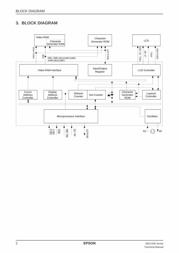
3. BLOCK DIAGRAM
Video RAM
CharacterGenerator RAM
CharacterGenerator ROM
LCD ControllerVideo RAM Interface
DisplayAddress
Controller
CursorAddress
Controller
RefreshCounter Dot Counter
CharacterGenerator
ROM
LayeredController
Oscillator
YS
CL,
YD
, YD
IS
LP, W
F
XS
CL
XD
0 to
XD
3
VD
0 to
VD
7
VA
0 to
VA
15
VC
E
VRD, VWR (SED1335F/1336F)VR/W (SED1330F)
SE
L0S
EL1
RE
S
RD
, WR
A0,
CS
D0
to D
7
XG XD
Input/OutputRegister
LCD
Microprocessor Interface
BLOCK DIAGRAM
SED1335 Series EPSON 3Technical Manual
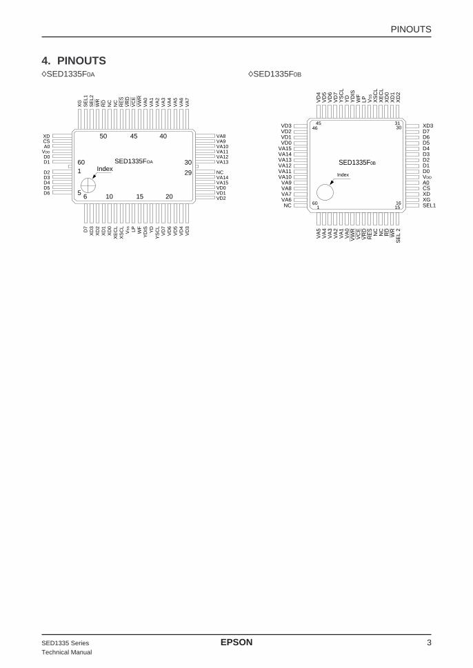
4. PINOUTS◊SED1335F0A ◊SED1335F0B
Index
1 15
314546
60
SED1335F0B
16
30 XD3D7D6D5D4D3D2D1D0VDD
A0CSXDXGSEL1
VD3VD2VD1VD0
VA15VA14VA13VA12VA11VA10VA9VA8VA7VA6NC
VD
4V
D5
VD
6V
D7
YS
CL
YD
YD
ISW
FLP V
SS
XS
CL
XE
CL
XD
0X
D1
XD
2
VA
5V
A4
VA
3V
A2
VA
1V
A0
VW
RV
CE
VR
DR
ES
NC
NC
RD
WR
SE
L 2
Index13060
5
29
404550
201510
SED1335FOA
VA8VA9VA10VA11VA12VA13
NCVA14VA15VD0VD1VD2
XDCSA0
VDD
D0D1
D2D3D4D5D6
D7
XD
3X
D2
XD
1X
D0
XE
CL
XS
CL
VS
S
LP WF
YD
IS YD
YS
CL
VD
7V
D6
VD
5V
D4
VD
3
XG
SE
L1S
EL2
WR
RD
NC
NC
RE
SV
RD
VC
EV
WR
VA
0V
A1
VA
2V
A3
VA
4V
A5
VA
6V
A7
6
PINOUTS
4 EPSON SED1335 SeriesTechnical Manual
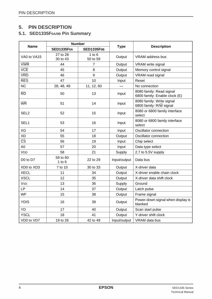
5. PIN DESCRIPTION5.1. SED1335F0A/0B Pin Summary
NameNumber
Type DescriptionSED1335F0A SED1335F0B
VA0 to VA1527 to 28 1 to 6
Output VRAM address bus30 to 43 50 to 59
VWR 44 7 Output VRAM write signal
VCE 45 8 Output Memory control signal
VRD 46 9 Output VRAM read signal
RES 47 10 Input Reset
NC 28, 48, 49 11, 12, 60 — No connection
RD 50 13 Input8080 family: Read signal6800 family: Enable clock (E)
WR 51 14 Input8080 family: Write signal6800 family: R/W signal
SEL2 52 15 Input8080 or 6800 family interfaceselect
SEL1 53 16 Input8080 or 6800 family interfaceselect
XG 54 17 Input Oscillator connection
XD 55 18 Output Oscillator connection
CS 56 19 Input Chip select
A0 57 20 Input Data type select
VDD 58 21 Supply 2.7 to 5.5V supply
D0 to D759 to 60
22 to 29 Input/output Data bus1 to 6
XD0 to XD3 7 to 10 30 to 33 Output X-driver data
XECL 11 34 Output X-driver enable chain clock
XSCL 12 35 Output X-driver data shift clock
VSS 13 36 Supply Ground
LP 14 37 Output Latch pulse
WF 15 38 Output Frame signal
YDIS 16 39 OutputPower-down signal when display isblanked
YD 17 40 Output Scan start pulse
YSCL 18 41 Output Y-driver shift clock
VD0 to VD7 19 to 26 42 to 49 Input/output VRAM data bus
PIN DESCRIPTION

SED1335 Series EPSON 5Technical Manual
5.2. Pin Functions5.2.1. Power supply
5.2.3. Microprocessor interface
5.2.2. Oscillator
Pin Name Function
VDD2.7 to 5.5V supply.This may be the same supply as the controlling microprocessor.
VSS Ground
Note: The peak supply current drawn by the SED1335 series may be up to ten times the average supply current. The powersupply impedance must be kept as low as possible by ensuring that supply lines are sufficiently wide and by placing 0.47 µFdecoupling capacitors that have good high-frequency response near the device’s supply pins.
Pin Name Function
XGCrystal connection for internal oscillator (See section 13). This pin can be driven by an externalclock source that satisfies the timing specifications of the EXT φ0 signal (See section 6.3.6).
XDCrystal connection for internal oscillator. Leave this pin open when using an external clocksource.
Pin Name Function
D0 to D7 Tristate input/output pins. Connect these pins to an 8- or 16-bit microprocessor bus.
Microprocessor interface select pin. The SED1335 series supports both 8080 family processors (such as the 8085 and Z80®) and 6800 family processors (such as the 6802 and 6809).
SEL1 SEL2* Interface A0 RD WR CS
0 0 8080 family A0 RD WR CS
1 0 6800 family A0 E R/W CS
Note: SEL1 should be tied directly to VDD or VSS to prevent noise. If noise does appear on SEL1, decouple it to ground using acapacitor placed as close to the pin as possible.
SEL1, SEL2
PIN DESCRIPTION

6 EPSON SED1335 SeriesTechnical Manual
5.2.4. Display memory controlThe SED1335 series can directly access static RAM andPROM. The designer may use a mixture of these two
types of memory to achieve an optimum trade-off be-tween low cost and low power consumption.
Pin Name Function
8080 family interface
A0 RD WR Function
0 0 1 Status flag read
1 0 1 Display data and cursor address read
0 1 0 Display data and parameter write
1 1 0 Command write
6800 family interface
A0 R/W E Function
0 1 1 Status flag read
1 1 1 Display data and cursor address read
0 0 1 Display data and parameter write
1 0 1 Command write
When the 8080 family interface is selected, this signal acts as the active-LOW read strobe. The SED1335 series output buffers are enabled when this signal is active.
When the 6800 family interface is selected, this signal acts as the active-HIGH enable clock. Data is read from or written to the SED1335 series when this clock goes HIGH.
When the 8080 family interface is selected, this signal acts as the active-LOW write strobe. The bus data is latched on the rising edge of this signal.
When the 6800 family interface is selected, this signal acts as the read/write control signal. Data is read from the SED1335 series if this signal is HIGH, and written to the SED1335 series if it is LOW.
Chip select. This active-LOW input enables the SED1335 series. It is usually connected to the output of an address decoder device that maps the SED1335 series into the memory space of the controlling microprocessor.
This active-LOW input performs a hardware reset on the SED1335 series. It is a Schmitt-trigger input for enhanced noise immunity; however, care should be taken to ensurethat it is not triggered if the supply voltage is lowered.
WR or R/W
CS
RES
RD or E
A0
VA0 to VA1516-bit display memory address. When accessing character generator RAM or ROM, VA0 toVA3, reflect the lower 4 bits of the SED1335 series’s row counter.
VD0 to VD7 8-bit tristate display memory data bus. These pins are enabled when VR/W is LOW.
VCE Active-LOW static memory standby control signal. VCE can be used with CS.
VWR Active-LOW display memory write control output.
Pin Name Function
VRD Active-LOW display memory read control output.
PIN DESCRIPTION
SED1335 Series EPSON 7Technical Manual
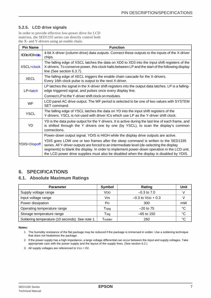
5.2.5. LCD drive signalsIn order to provide effective low-power drive for LCDmatrixes, the SED1335 series can directly control boththe X- and Y-drivers using an enable chain.
Pin Name Function
XD0 to XD3=data4-bit X-driver (column drive) data outputs. Connect these outputs to the inputs of the X-driverchips.
The falling edge of XSCL latches the data on XD0 to XD3 into the input shift registers of theX-drivers. To conserve power, this clock halts between LP and the start of the following displayline (See section 6.3.7).
XECLThe falling edge of XECL triggers the enable chain cascade for the X-drivers. Every 16th clock pulse is output to the next X-driver.
LP latches the signal in the X-driver shift registers into the output data latches. LP is a falling-edge triggered signal, and pulses once every display line.
Connect LP to the Y-driver shift clock on modules.
WFLCD panel AC drive output. The WF period is selected to be one of two values with SYSTEMSET command.
The falling edge of YSCL latches the data on YD into the input shift registers of the Y-drivers. YSCL is not used with driver ICs which use LP as the Y-driver shift clock.
YD is the data pulse output for the Y drivers. It is active during the last line of each frame, andis shifted through the Y drivers one by one (by YSCL), to scan the display’s commonconnections.
Power-down output signal. YDIS is HIGH while the display drive outputs are active.
YDIS goes LOW one or two frames after the sleep command is written to the SED1335series. All Y-driver outputs are forced to an intermediate level (de-selecting the displaysegments) to blank the display. In order to implement power-down operation in the LCD unit,the LCD power drive supplies must also be disabled when the display is disabled by YDIS.
XSCL=clock
LP=latch
YSCL
YD
YDIS=Dispoff
PIN DESCRIPTION/SPECIFICATIONS
6. SPECIFICATIONS6.1. Absolute Maximum Ratings
Parameter Symbol Rating Unit
Supply voltage range VDD –0.3 to 7.0
Input voltage range VIN –0.3 to VDD + 0.3 V
V
Power dissipation PD 300 mW
Operating temperature range Topg –20 to 75 °CStorage temperature range Tstg –65 to 150 °CSoldering temperature (10 seconds). See note 1. Tsolder 260 °C
Notes:
1. The humidity resistance of the flat package may be reduced if the package is immersed in solder. Use a soldering techniquethat does not heatstress the package.
2. If the power supply has a high impedance, a large voltage differential can occur between the input and supply voltages. Takeappropriate care with the power supply and the layout of the supply lines. (See section 6.2.)
3. All supply voltages are referenced to VSS = 0V.

8 EPSON SED1335 SeriesTechnical Manual
6.2. SED1335
Notes:
Parameter Symbol ConditionRating
Unitmin typ max
Supply voltage VDD 4.5 5.0 5.5 V
Register data retention voltage VOH 2.0 — 6.0 V
Input leakage current ILI VI = VDD. See note 5. — 0.05 2.0 µA
Output leakage current ILO VI = VSS. See note 5. — 0.10 5.0 µA
Operating supply current Iopr See note 4. — 11 15 mA
Quiescent supply current IQSleep mode,
— 0.05 20.0 µAVOSC1 = VCS = VRD = VDD
Oscillator frequency fOSC 1.0 — 10.0 MHz
External clock frequency fCL 1.0 — 10.0 MHz
Oscillator feedback resistance Rf 0.5 1.0 3.0 MΩTTL
HIGH-level input voltage VIHT See note 1. 0.5VDD — VDD V
LOW-level input voltage VILT See note 1. VSS — 0.2VDD V
HIGH-level output voltage VOHTIOH = –5.0 mA.
2.4 — — VSee note 1.
LOW-level output voltage VOLT IOL = 5.0 mA. See note 1. — — VSS + 0.4 V
CMOS
HIGH-level input voltage VIHC See note 2. 0.8VDD — VDD V
LOW-level input voltage VILC See note 2. VSS — 0.2VDD V
HIGH-level output voltage VOHC IOH = –2.0 mA. See note 2.VDD – 0.4 — — V
LOW-level output voltage VOLC IOH = 1.6 mA. See note 2. — — VSS + 0.4 V
Open-drain
LOW-level output voltage VOLN IOL = 6.0 mA. SS + 0.4 V
Schmitt-trigger
Rising-edge threshold voltage VT+ See note 3. 0.5VDD 0.7VDD 0.8VDD V
Falling-edge threshold voltage VT– See note 3. 0.2VDD 0.3VDD 0.5VDD V
VDD = 4.5 to 5.5V, VSS = 0V, Ta = –20 to 75°C
Measured at crystal,47.5% duty cycle.
See note 6.
1. D0 to D7, A0, CS, RD, WR, VD0 to VD7, VA0 to VA15, VRD, VWR and VCE are TTL-level inputs.
2. SEL1 is CMOS-level inputs. YD, XD0 to XD3, XSCL, LP, WF, YDIS are CMOS-level outputs.
3. RES is a Schmitt-trigger input. The pulsewidth on RES must be at least 200 µs. Note that pulses of more than a few seconds will cause DC voltages to be applied to the LCD panel.
4. fOSC = 10 MHz, no load (no display memory), internal character generator, 256 × 200 pixel display. The operating supply current can be reduced by approximately 1 mA by setting both CLO and the display OFF.
5. VD0 to VD7 and D0 to D7 have internal feedback circuits so that if the inputs become high-impedance, the input state immediately prior to that is held. Because of the feedback circuit, input current flow occurs when the inputs are in an intermediate state.
6. Because the oscillator circuit input bias current is in the order of µA, design the printed circuit board so as to reduce leakage currents.
— — V
SPECIFICATIONS

SED1335 Series EPSON 9Technical Manual
Notes1. D0 to D7, A0, CS, RD, WR, VD0 to VD7, VA0 to VA15, VRD, VWR and VCE are TTL-level inputs.
2. SEL1 is CMOS-level inputs. YD, XD0 to XD3, XSCL, LP, WF, YDIS are CMOS-level outputs.
3. RES is a Schmitt-trigger input. The pulsewidth on RES must be at least 200 µs. Note that pulses of more than a few seconds willcause DC voltages to be applied to the LCD panel.
4. fOSC = 10 MHz, no load (no display memory), internal character generator, 256 × 200 pixel display. The operating supply current canbe reduced by approximately 1 mA by setting both CLO and the display OFF.
5. VD0 to VD7 and D0 to D7 have internal feedback circuits so that if the inputs become high-impedance, the input state immediatelyprior to that is held. Because of the feedback circuit, input current flow occurs when the inputs are in an intermediate state.
6. Because the oscillator circuit input bias current is in the order of µA, design the printed circuit board so as to reduce leakage currents.
VDD = 2.7 to 4.5 V, VSS = 0 V, Ta = –20 to 75˚C unless otherwise noted
Parameter Symbol ConditionRating
Unitmin typ max
Supply voltage VDD 2.7 3.5 4.5 V
Register data retention voltage VOH 2.0 — 6.0 V
Input leakage current ILI VI = VDD. See note 5. — 0.05 2.0 µA
Output leakage current ILO VI = VSS. See note 5. — 0.10 5.0 µA
Operating supply current IoprVDD = 3.5 V. See note 4. — 3.5 —
mASee note 4. — — 7.0
Quiescent supply current IQSleep mode,
— 0.05 20.0 µAVOSC1 = VCS = VRD = VDD
Oscillator frequency fOSC Measured at crystal, 1.0 — 8.0 MHz
External clock frequency fCL 47.5% duty cycle. 1.0 — 8.0 MHz
Oscillator feedback resistance Rf See note 6. 0.7 — 3.0 MΩ
TTL
HIGH-level input voltage VIHT See note 1. 0.5 VDD — VDD V
LOW-level input voltage VILT See note 1. VSS — 0.2 VDD V
HIGH-level output voltage VOHT IOH = –3.0 mA. See note 1. 2.4 — — V
LOW-level output voltage VOLT IOL = 3.0 mA. See note 1. — — VSS + 0.4 V
CMOS
HIGH-level input voltage VIHC See note 2. 0.8 VDD — VDD V
LOW-level input voltage VILC See note 2. VSS — 0.2 VDD V
HIGH-level output voltage VOHC IOH = –2.0 mA. See note 2. VDD – 0.4 — — V
LOW-level output voltage VOLC IOH = 1.6 mA. See note 2. — — VSS + 0.4 V
Open-drain
LOW-level output voltage VOLN IOL = 6.0 mA. — — VSS + 0.4 V
Schmitt-trigger
Rising-edge threshold voltage VT+ See note 3. 0.5 VDD 0.7 VDD 0.8 VDD V
Falling-edge threshold voltage VT– See note 3. 0.2 VDD 0.3 VDD 0.5 VDD V
SPECIFICATIONS
10 EPSON SED1335 SeriesTechnical Manual
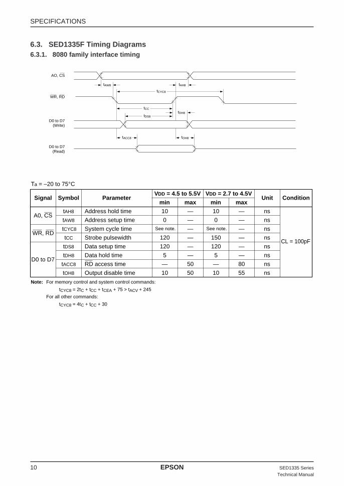
6.3. SED1335F Timing Diagrams6.3.1. 8080 family interface timing
tCYC8
tOH8
tAH8tAW8
tCC
tDS8tDH8
tACC8
AO, CS
WR, RD
D0 to D7(Write)
D0 to D7(Read)
Signal Symbol ParameterVDD = 4.5 to 5.5V VDD = 2.7 to 4.5V
Unit Conditionmin max min max
A0, CStAH8 Address hold time 10 — 10 — ns
tAW8 Address setup time 0 — 0 — ns
WR, RDtCYC8 System cycle time See note. — See note. — ns
tCC Strobe pulsewidth 120 — 150 — nsCL = 100pF
tDS8 Data setup time 120 — 120 — ns
D0 to D7tDH8 Data hold time 5 — 5 — ns
tACC8 RD access time — 50 — 80 ns
tOH8 Output disable time 10 50 10 55 ns
Note: For memory control and system control commands:
tCYC8 = 2tC + tCC + tCEA + 75 > tACV + 245
For all other commands:
tCYC8 = 4tC + tCC + 30
Ta = –20 to 75°C
SPECIFICATIONS

SED1335 Series EPSON 11Technical Manual
6.3.2. 6800 family interface timing
Note: tCYC6 indicates the interval during which CS is LOW and E is HIGH.
E
R/W
A0, CS
D0 to D7(Write)
D0 to D7(Read)
tCYC6
tAW6 tEW
tAH6
tDH6tDS6
tOH6tACC6
SPECIFICATIONS
A0,CS,R/W
Signal Symbol ParameterVDD = 4.5 to 5.5V VDD = 2.7 to 4.5V
Unit Conditionmin max min max
tCYC6 System cycle time See note. — See note. — ns
tAW6 Address setup time 0 — 10 — ns
tAH6 Address hold time 0 — 0 — ns
tDS6 Data setup time 100 — 120 — ns CL =
D0 to D7tDH6 Data hold time 0 — 0 — ns 100 pF
tOH6 Output disable time 10 50 10 75 ns
tACC6 Access time — 85 — 130 ns
E tEW Enable pulsewidth 120 — 150 — ns
Note: For memory control and system control commands:
tCYC6 = 2tC + tEW + tCEA + 75 > tACV + 245
For all other commands:
tCYC6 = 4tC + tEW + 30
Ta = –20 to 75°C
12 EPSON SED1335 SeriesTechnical Manual
6.3.3. Display memory read timing
EXTΦ0
VCE
VA0 to VA15
VR/W
VD0 to VD7
tC
tW tCE tW
tAHCtASC
tCYR
tRCS tCEA
tRCH
tCE3
tOH2tACV
Signal Symbol ParameterVDD = 4.5 to 5.5V VDD = 2.7 to 4.5V
Unit Conditionmin max min max
EXT φ0 tC Clock period 100 — 125 — ns
tWVCE HIGH-level pulsewidth
tC – 50 — tC – 50 — nsVCE
tCEVCE LOW-level pulsewidth
2tC – 30 — 2tC – 30 — ns
tCYR Read cycle time 3tC — 3tC — ns
tASCAddress setup time to
tC – 70 — tC – 100 — nsfalling edge of VCE
tAHCAddress hold time from
2tC – 30 — 2tC – 40 — nsfalling edge of VCE
tRCSRead cycle setup time to
tC – 45 — tC – 60 — nsVRD
falling edge of VCE
tRCHRead cycle hold time
0.5tC — 0.5tC — nsfrom rising edge of VCE
tACV Address access time — 3tC – 100 — 3tC – 115 ns
VD0 to tCEA VCE access time — 2tC – 80 — 2tC – 90 nsVD7 tOH2 Output data hold time 0 — 0 — ns
tCE3 VCE to data off time 0 — 0 — ns
VA0 toVA15 CL = 100
pF
Ta = –20 to 75°C
SPECIFICATIONS

SED1335 Series EPSON 13Technical Manual
6.3.4. Display memory write timing
tWSC
tC
tCE
tAH2
tCA
tDH2
tASC
tWHCtAS
tDHCtDSC
tAHC
tW
EXT φ O
VCE
VA0 to VA15
VR/W
VD0 to VD7
SPECIFICATIONS

14 EPSON SED1335 SeriesTechnical Manual
Signal Symbol ParameterVDD = 4.5 to 5.5V VDD = 2.7 to 4.5V
Unit Conditionmin max min max
EXT φ0 tC Clock period 100 — 125 — ns
tWVCE HIGH-level pulsewidth
tC – 50 — tC – 50 — nsVCE
tCEVCE LOW-level pulsewidth 2tC – 30 — 2tC – 30 — ns
tCYW Write cycle time 3tC — 3tC — ns
tAHCAddress hold time from
2tC – 30 — 2tC – 40 — nsfalling edge of VCE
tASCAddress setup time to
tC – 70 — tC – 110 — nsfalling edge of VCE
VA0 totCA
Address hold time from0 — 0 — nsVA15 rising edge of VCE
tASAddress setup time to
0 — 0 — nsfalling edge of VWR
tAH2Address hold time from
10 — 10 — nsrising edge of VWR
tWSCWrite setup time to
tC – 80 — tC – 115 — nsVWR
falling edge of VCE
tWHCWrite hold time from
2tC – 20 — 2tC – 20 — nsfalling edge of VCE
tDSCData input setup time to
tC – 85 — tC – 125 — nsfalling edge of VCE
VD0 totDHC
Data input hold time2tC – 30 — 2tC – 30 — ns
VD7 from falling edge of VCE
tDH2Data hold time from
5 50 5 50 nsrising edge of VWR
Note: VD0 to VD7 are latching input/outputs. While the bus is high impedance, VD0 to VD7 retain the write data until the data readfrom the memory is placed on the bus.
Ta = –20 to 75°C
CL = 100pF
SPECIFICATIONS
SED1335 Series EPSON 15Technical Manual
6.3.5. SLEEP IN command timing
VCE
WR(Command input)
YDIS
tWRL tWRD
SYSTEM SET writeSLEEP IN write
Signal Symbol ParameterVDD = 4.5 to 5.5V VDD = 2.7 to 4.5V
Unit Conditionmin max min max
tWRDVCE falling-edge delay
See note 1. — See note 1. — nsWR
time
tWRLYDIS falling-edge delay
— See note 2. — See note 2. nstime
Notes:
1. tWRD = 18tC + tOSS + 40 (tOSS is the time delay from the sleep state until stable operation)
2. tWRL = 36tC × [TC/R] × [L/F] + 70
Ta = –20 to 75°C
CL = 100pF
SPECIFICATIONS
16 EPSON SED1335 SeriesTechnical Manual
6.3.6. External oscillator signal timing
EXTφ0
tWL tWH
tC
tRCL tFCL
See note 1. See note 2. See note 1. See note 2.
Signal Symbol ParameterVDD = 4.5 to 5.5V VDD = 2.7 to 4.5V
Unit Conditionmin max min max
tRCL External clock rise time — 15 — 15 ns
tFCL External clock fall time — 15 — 15 ns
tWHExternal clock
See note 1. See note 2. See note 1. See note 2. nsHIGH-level pulsewidth
tWLExternal clock
nsLOW-level pulsewidth
tC External clock period 100 — 125 — ns
Notes:
1. (tC – tRCL – tFCL) × 475 < tWH, tWL1000
2.(tC – tRCL – tFCL) × 525
> tWH, tWL1000
Ta = –20 to 75°C
EXT φ0
SPECIFICATIONS
SED1335 Series EPSON 17Technical Manual
6.3.7. LCD output timingThe following characteristics are for a 1/64 duty cycle.
Row
LP
LP
XSCL
tr
(14) (15) (16) (1) (15) (15)(16) (16)(1) (3) (1)(2)
tftWX tCX
tDS tDH
tLS
tWL
tDF
tLD
tDHY
LP
YD
XD0 to XD3
WF(B)
XSCL
XD0 to XD3
YD
WF
WF
Row 64 Row 1
1 line time
1 frame time
62 63 64 1 2 3 4 60 61 62 63 64
Row 2
SPECIFICATIONS

18 EPSON SED1335 SeriesTechnical Manual
Signal Symbol ParameterVDD = 4.5 to 5.5V VDD = 2.7 to 4.5V
Unit Conditionmin max min max
tr Rise time — 30 — 40 ns
tf Fall time — 30 — 40 ns
XSCLtCX Shift clock cycle time 4tC — 4tC — ns
tWX XSCL clock pulsewidth 2tC – 60 — 2tC – 60 — ns
XD0 to tDH X data hold time 2tC – 50 — 2tC – 50 — nsXD3 tDS X data setup time 2tC – 100 — 2tC – 105 — ns
tLS Latch data setup time 2tC – 50 — 2tC – 50 — ns
LP tWL LP pulsewidth 4tC – 80 — 4tC – 120 — ns
tLD LP delay time from XSCL 0 — 0 — ns
WF tDF Permitted WF delay — 50 — 50 ns
YD tDHY Y data hold time 2tC – 20 — 2tC – 20 — ns
Ta = –20 to 75°C
CL =100 pF
SPECIFICATIONS

SED1335 Series EPSON 19Technical Manual
7. PACKAGE DIMENSIONSUnit: mm
7.1. SED1335F0A
◊QFP5-60 pin
7.2. SED1335F0B
◊QFP6-60 pin
0 to 12°
2.8
2.7
± 0.
1
1.5 ± 0.3
0.15
± 0
.05
Index
6 23
36
24
54
55
130
0.35 ± 0.1
19.6
± 0
.4
14.0
± 0
.1
25.6 ± 0.4
20.0 ± 0.1
60
5
29
35
1.0 ± 0.1
Index
1 15
31
16
45
46
60
30
0 to 12°
1.8
2.7
± 0.
1
0.8 ± 0.3
0.15
± 0
.05
0.35 ± 0.150.8 ± 0.15
17.6
± 0
.4
14.0
± 0
.2
17.6 ± 0.4
14.0 ± 0.2
PACKAGE DIMENSIONS
20 EPSON SED1335 SeriesTechnical Manual
8. INSTRUCTION SET8.1. The Command SetTable 1. Command set
CommandCode Read
Class Command Hex Command Description Parameters
RD WR A0 D7 D6 D5 D4 D3 D2 D1 D0No. of Sec-Bytes tion
SYSTEM SET 1 0 1 0 1 0 0 0 0 0 0 40Initialize device and
8 8.2.1display
SLEEP IN 1 0 1 0 1 0 1 0 0 1 1 53 Enter standby mode 0 8.2.2
DISP ON/OFF 1 0 1 0 1 0 1 1 0 0 D58, Enable and disable dis-
1 8.3.159 play and display flashing
SCROLL 1 0 1 0 1 0 0 0 1 0 0 44Set display start address
10 8.3.2and display regions
CSRFORM 1 0 1 0 1 0 1 1 1 0 1 5D Set cursor type 2 8.3.3
CGRAM ADR 1 0 1 0 1 0 1 1 1 0 0 5CSet start address of char-
2 8.3.6acter generator RAM
CD CD4C
Set direction of cursorCSRDIR 1 0 1 0 1 0 0 1 1
1 0to
movement0 8.3.4
4F
HDOT SCR 1 0 1 0 1 0 1 1 0 1 0 5ASet horizontal scroll
1 8.3.7position
OVLAY 1 0 1 0 1 0 1 1 0 1 1 5BSet display overlay
1 8.3.5format
CSRW 1 0 1 0 1 0 0 0 1 1 0 46 Set cursor address 2 8.4.1
CSRR 1 0 1 0 1 0 0 0 1 1 1 47 Read cursor address 2 8.4.2
MWRITE 1 0 1 0 1 0 0 0 0 1 0 42 Write to display memory — 8.5.1
MREAD 1 0 1 0 1 0 0 0 0 1 1 43Read from display
— 8.5.2memory
Notes:
1. In general, the internal registers of the SED1335 series are modified as each command parameter is input. However,the microprocessor does not have to set all the parameters of a command and may send a new command before all parametershave been input. The internal registers for the parameters that have been input will have been changed but the remainingparameter registers are unchanged.
2-byte parameters (where two bytes are treated as 1 data item) are handled as follows:
a. CSRW, CSRR: Each byte is processed individually. The microprocessor may read or write just the low byte of the cursoraddress.
b. SYSTEM SET, SCROLL, CGRAM ADR: Both parameter bytes are processed together. If the command is changed afterhalf of the parameter has been input, the single byte is ignored.
2. APL and APH are 2-byte parameters, but are treated as two 1-byte parameters.
Systemcontrol
Displaycontrol
Drawingcontrol
Memorycontrol
INSTRUCTION SET

SED1335 Series EPSON 21Technical Manual
8.2. System Control Commands8.2.1. SYSTEM SETInitializes the device, sets the window sizes, and selectsthe LCD interface format. Since this command sets thebasic operating parameters of the SED1335 series, an
incorrect SYSTEM SET command may cause othercommands to operate incorrectly.
8.2.1.1. C
This control byte performs the following:1. Resets the internal timing generator2. Disables the display3. Cancels sleep modeParameters following P1 are not needed if only can-celing sleep mode.
8.2.1.2. M0
Selects the internal or external character generator ROM.The internal character generator ROM contains 160, 5 ×7 pixel characters, as shown in figure 70. These charac-ters are fixed at fabrication by the metallization mask.The external character generator ROM, on the otherhand, can contain up to 256 user-defined characters.M0 = 0: Internal CG ROMM0 = 1: External CG ROM
Note that if the CG ROM address space overlaps thedisplay memory address space, that portion of the displaymemory cannot be written to.
8.2.1.3. M1
Selects the memory configuration for user-definable char-acters. The CG RAM codes select one of the 64 codesshown in figure 46.M1 = 0: No D6 correction.The CG RAM1 and CG RAM2 address spaces are notcontiguous, the CG RAM1 address space is treated ascharacter generator RAM, and the CG RAM2 addressspace is treated as character generator ROM.M1 = 1: D6 correction.The CG RAM1 and CG RAM2 address spaces arecontiguout and are both treated as character generatorRAM.
C 0 1 0 0 0 0 0 0 1 0 1
D7 D6 D5 D4 D3 D2 D1 D0 A0 WR RD
P1 0 0 IV 1 W/S M2 M1 M0 0 0 1
P2 WF 0 0 0 0 FX 0 0 1
P3 0 0 0 0 FY 0 0 1
P4 C/R 0 0 1
P5 TC/R 0 0 1
P6 L/F 0 0 1
P7 APL 0 0 1
P8 APH 0 0 1
LSBMSB
Figure 1. SYSTEM SET instruction
INSTRUCTION SET
22 EPSON SED1335 SeriesTechnical Manual
8.2.1.4. M2
Selects the height of the character bitmaps. Charactersmore than 16 pixels high can be displayed by creating abitmap for each portion of each character and using theSED1335 series graphics mode to reposition them.M2 = 0: 8-pixel character height (2716 or equivalentROM)M2 = 1: 16-pixel character height (2732 or equivalentROM)
8.2.1.5. W/S
Selects the LCD drive method.W/S = 0: Single-panel driveW/S = 1: Dual-panel drive
EI X driver X driver
LCDY driver
YD
Figure 2. Single-panel display
Figure 3. Above and below two-panel display
EI X driver X driver
YD
X driver X driver
Upper Panel
Lower Panel
Y driver
INSTRUCTION SET
SED1335 Series EPSON 23Technical Manual
Figure 4. Left-and-right two-panel display
NoteThere are no Seiko Epson LCD units in the configuration shown in Figure 4.
Table 2. LCD parameters
8.2.1.6. IV
Screen origin compensation for inverse display. IV isusually set to 1.The best way of displaying inverted characters is toExclusive-OR the text layer with the graphics back-ground layer. However, inverted characters at the top or
left of the screen are difficult to read as the characterorigin is at the top-left of its bitmap and there are nobackground pixels either above or to the left of thesecharacters.
EI
YD
Y driver
X driver X driver X driver X driver
Right PanelLeft Panel
ParameterW/S = 0 W/S = 1
IV = 1 IV = 0 IV = 1 IV = 0
C/R C/R C/R C/R C/R
TC/R TC/R TC/R (See note 1.) TC/R TC/R
L/F L/F L/F L/F L/F
SL1 00H to L/F00H to L/F + 1
(L/F) / 2 (L/F) / 2(See note 2.)
SL2 00H to L/F00H to L/F + 1
(L/F) / 2 (L/F) / 2(See note 2.)
SAD1 First screen block First screen block First screen block First screen block
SAD2 Second screen block Second screen block Second screen block Second screen block
SAD3 Third screen block Third screen block Third screen block Third screen block
SAD4 Invalid Invalid Fourth screen block Fourth screen block
Cursor move-Continuous movement over whole screen
Above-and-below configuration:ment range continuous movement over whole screen
Notes:
1. See table 26 for further details on setting the C/R and TC/R parameters when using the HDOT SCR command.
2. The value of SL when IV = 0 is equal to the value of SL when IV = 1, plus one.
INSTRUCTION SET
24 EPSON SED1335 SeriesTechnical Manual
The IV flag causes the SED1335 series to offset the textscreen against the graphics back layer by one verticalpixel. Use the horizontal pixel scroll function (HDOTSCR) to shift the text screen 1 to 7 pixels to the right. Allcharacters will then have the necessary surrounding back-ground pixels that ensure easy reading of the invertedcharacters.See Section 10.5 for information on scrolling.IV = 0: Screen top-line correctionIV = 1: No screen top-line correction
Figure 5. IV and HDOT SCR adjustment
8.2.1.7. FX
Define the horizontal character size. The character widthin pixels is equal to FX + 1, where FX can range from 00to 07H inclusive. If data bit 3 is set (FX is in the range 08to 0FH) and an 8-pixel font is used, a space is insertedbetween characters.
Table 3. Horizontal character size selection
IV
1 dot
Dots 1 to 7
Display start point
Back layer
HDOT SCR
CharacterSince the SED1335 series handles display data in 8-bitunits, characters larger than 8 pixels wide must be formedfrom 8-pixel segments. As Figure 6 shows, the remainderof the second eight bits are not displayed. This alsoapplies to the second screen layer.In graphics mode, the normal character field is also eightpixels. If a wider character field is used, any remainder inthe second eight bits is not displayed.
FX [FX] character widthHEX D3 D2 D1 D0 (pixels)
00 0 0 0 0 1
01 0 0 0 1 2
↓ ↓ ↓ ↓ ↓ ↓07 0 1 1 1 8
Figure 6. FX and FY display addresses
8 bits
FY
FX
8 bits
FY
FX
Non-display areaAddress BAddress A
8 bits
8 bits
INSTRUCTION SET

SED1335 Series EPSON 25Technical Manual
8.2.1.8. WF
Selects the AC frame drive waveform period. WF isusually set to 1.WF = 0: 16-line AC driveWF = 1: two-frame AC driveIn two-frame AC drive, the WF period is twice the frameperiod.In 16-line AC drive, WF inverts every 16 lines.Although 16-line AC drive gives a more readable display,horizontal lines may appear when using high LCD drivevoltages or at high viewing angles.
8.2.1.9. FY
Sets the vertical character size. The height in pixels isequal to FY + 1.FY can range from 00 to 0FH inclusive.Set FY to zero (vertical size equals one) when in graphicsmode.
Table 4. Vertical character size selection
FY [FY] characterHEX D3 D2 D1 D0 height (pixels)
00 0 0 0 0 1
01 0 0 0 1 2
↓ ↓ ↓ ↓ ↓ ↓07 0 1 1 1 8
↓ ↓ ↓ ↓ ↓ ↓0E 1 1 1 0 15
0F 1 1 1 1 16
8.2.1.10. C/R
Sets the address range covered by one display line, that is,the number of characters less one, multiplied by thenumber of horizontal bytes per character.C/R can range from 0 to 239.For example, if the character width is 10 pixels, then theaddress range is equal to twice the number of characters,less 2. See Section 16.1.1 for the calculation of C/R.[C/R] cannot be set to a value greater than the addressrange. It can, however, be set smaller than the addressrange, in which case the excess display area is blank. Thenumber of excess pixels must not exceed 64.
Table 5. Display line address range
C/R[C/R] bytes per display line
HEX D7 D6 D5 D4 D3 D2 D1 D0
00 0 0 0 0 0 0 0 0 1
01 0 0 0 0 0 0 0 1 2
↓ ↓ ↓ ↓ ↓ ↓ ↓ ↓ ↓ ↓4F 0 1 0 0 1 1 1 1 80
↓ ↓ ↓ ↓ ↓ ↓ ↓ ↓ ↓ ↓EE 1 1 1 0 1 1 1 0 239
EF 1 1 1 0 1 1 1 1 240
INSTRUCTION SET

26 EPSON SED1335 SeriesTechnical Manual
8.2.1.11. TC/R
Sets the length, including horizontal blanking, of oneline. The line length is equal to TC/R + 1, where TC/ R canrange from 0 to 255.TC/R must be greater than or equal to C/R + 4. Providedthis condition is satisfied, [TC/R] can be set according to
the equation given in section 16.1.1 in order to hold theframe period constant and minimize jitter for any givenmain oscillator frequency, fOSC.
Table 6. Line length selection
TC/R[TC/R] line length (bytes)
HEX D7 D6 D5 D4 D3 D2 D1 D0
00 0 0 0 0 0 0 0 0 1
01 0 0 0 0 0 0 0 1 2
↓ ↓ ↓ ↓ ↓ ↓ ↓ ↓ ↓ ↓52 0 1 0 1 0 0 1 0 83
↓ ↓ ↓ ↓ ↓ ↓ ↓ ↓ ↓ ↓FE 1 1 1 1 1 1 1 0 255
FF 1 1 1 1 1 1 1 1 256
8.2.1.12. L/F
Sets the height, in lines, of a frame. The height in lines isequal to L/F + 1, where L/F can range from 0 to 255.
Table 7. Frame height selection
If W/S is set to 1, selecting two-screen display, thenumber of lines must be even and L/F must, therefore, bean odd number.
L/F[L/F] lines per frame
HEX D7 D6 D5 D4 D3 D2 D1 D0
00 0 0 0 0 0 0 0 0 1
01 0 0 0 0 0 0 0 1 2
↓ ↓ ↓ ↓ ↓ ↓ ↓ ↓ ↓ ↓7F 0 1 1 1 1 1 1 1 128
↓ ↓ ↓ ↓ ↓ ↓ ↓ ↓ ↓ ↓FE 1 1 1 1 1 1 1 0 255
FF 1 1 1 1 1 1 1 1 256
INSTRUCTION SET
SED1335 Series EPSON 27Technical Manual
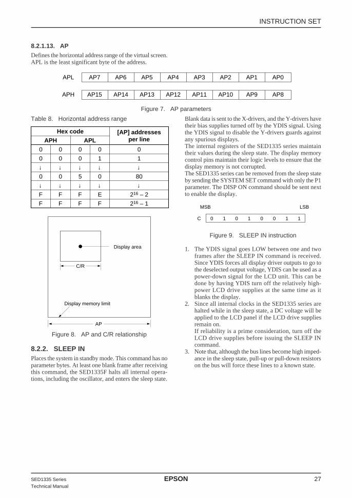
8.2.1.13. AP
Defines the horizontal address range of the virtual screen.APL is the least significant byte of the address.
Figure 8. AP and C/R relationship
8.2.2. SLEEP INPlaces the system in standby mode. This command has noparameter bytes. At least one blank frame after receivingthis command, the SED1335F halts all internal opera-tions, including the oscillator, and enters the sleep state.
Figure 7. AP parameters
APL AP7 AP6 AP5 AP4 AP3 AP2 AP1 AP0
APH AP15 AP14 AP13 AP12 AP11 AP10 AP9 AP8
Table 8. Horizontal address range
Hex code [AP] addressesAPH APL per line
0 0 0 0 0
0 0 0 1 1
↓ ↓ ↓ ↓ ↓0 0 5 0 80
↓ ↓ ↓ ↓ ↓F F F E 216 – 2
F F F F 216 – 1
Display area
C/R
Display memory limit
AP
Blank data is sent to the X-drivers, and the Y-drivers havetheir bias supplies turned off by the YDIS signal. Usingthe YDIS signal to disable the Y-drivers guards againstany spurious displays.The internal registers of the SED1335 series maintaintheir values during the sleep state. The display memorycontrol pins maintain their logic levels to ensure that thedisplay memory is not corrupted.The SED1335 series can be removed from the sleep stateby sending the SYSTEM SET command with only the P1parameter. The DISP ON command should be sent nextto enable the display.
Figure 9. SLEEP IN instruction
1. The YDIS signal goes LOW between one and twoframes after the SLEEP IN command is received.Since YDIS forces all display driver outputs to go tothe deselected output voltage, YDIS can be used as apower-down signal for the LCD unit. This can bedone by having YDIS turn off the relatively high-power LCD drive supplies at the same time as itblanks the display.
2. Since all internal clocks in the SED1335 series arehalted while in the sleep state, a DC voltage will beapplied to the LCD panel if the LCD drive suppliesremain on.If reliability is a prime consideration, turn off theLCD drive supplies before issuing the SLEEP INcommand.
3. Note that, although the bus lines become high imped-ance in the sleep state, pull-up or pull-down resistorson the bus will force these lines to a known state.
MSB LSB
C 0 1 0 1 0 0 1 1
INSTRUCTION SET

28 EPSON SED1335 SeriesTechnical Manual
8.3. Display Control Commands8.3.1. DISP ON/OFFTurns the whole display on or off. The single-byte param-eter enables and disables the cursor and layered screens,and sets the cursor and screen flash rates. The cursor canbe set to flash over one character or over a whole line.
Figure 10. DISP ON/OFF parameters
8.3.1.1. D
Turns the display ON or OFF. The D bit takes prece-dence over the FP bits in the parameter.D = 0: Display OFFD = 1: Display ON
8.3.1.2. FC
Enables/disables the cursor and sets the flash rate. Thecursor flashes with a 70% duty cycle (ON/OFF).
Table 9. Cursor flash rate selection
8.3.1.3. FP
Each pair of bits in FP sets the attributes of one screenblock, as follows.
The display attributes are as follows:
Table 10. Screen block attribute selection
NoteIf SAD4 is enabled by setting W/S to 1, FP3 and FP2control both SAD2 and SAD4. The attributes ofSAD2 and SAD4 cannot be set independently.
MSB LSB
C 0 1 0 1 1 0 0 D
P1 FP5 FP4 FP3 FP2 FP1 FP0 FC1 FC0
FC1 FC0 Cursor display
0 0 OFF (blank)
0 1 No flashing
1 0Flash at fFR/32 Hz
(approx. 2 Hz)
1 1Flash at fFR/64 Hz
(approx. 1 Hz)
Note: As the MWRITE command always enables the cursor,the cursor position can be checked even when perform-ing consecutive writes to display memory while thecursor is flashing.
ON
FP1 FP0 First screen block (SAD1)
FP3 FP2Second screen block (SAD2,
SAD4). See note.
FP5 FP4 Third screen block (SAD3)
0 0 OFF (blank)
0 1 No flashing
1 0Flash at fFR/32 Hz
(approx. 2 Hz)
1 1Flash at fFR/4 Hz(approx. 16 Hz)
ON
INSTRUCTION SET
SED1335 Series EPSON 29Technical Manual
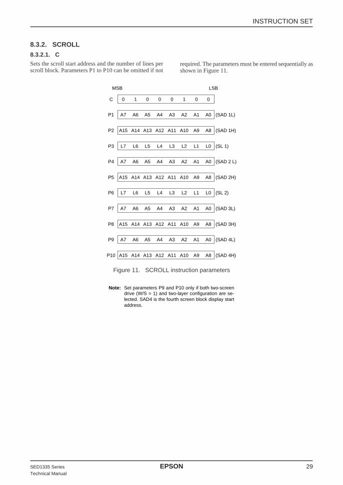
8.3.2. SCROLL
8.3.2.1. C
Sets the scroll start address and the number of lines perscroll block. Parameters P1 to P10 can be omitted if not
required. The parameters must be entered sequentially asshown in Figure 11.
MSB LSB
C 0 1 0 0 0 1 0 0
P1 A7 A6 A5 A4 A3 A2 A1 A0 (SAD 1L)
P2 A15 A14 A13 A12 A11 A10 A9 A8 (SAD 1H)
P3 L7 L6 L5 L4 L3 L2 L1 L0 (SL 1)
P4 A7 A6 A5 A4 A3 A2 A1 A0 (SAD 2 L)
P5 A15 A14 A13 A12 A11 A10 A9 A8 (SAD 2H)
P6 L7 L6 L5 L4 L3 L2 L1 L0 (SL 2)
P7 A7 A6 A5 A4 A3 A2 A1 A0 (SAD 3L)
P8 A15 A14 A13 A12 A11 A10 A9 A8 (SAD 3H)
P9 A7 A6 A5 A4 A3 A2 A1 A0 (SAD 4L)
P10 A15 A14 A13 A12 A11 A10 A9 A8 (SAD 4H)
Note: Set parameters P9 and P10 only if both two-screendrive (W/S = 1) and two-layer configuration are se-lected. SAD4 is the fourth screen block display startaddress.
Figure 11. SCROLL instruction parameters
INSTRUCTION SET

30 EPSON SED1335 SeriesTechnical Manual
8.3.2.2. SL1, SL2
SL1 and SL2 set the number of lines per scrolling screen.The number of lines is SL1 or SL2 plus one. The relation-
Table 11. Screen block start address selection
SL1, SL2[SL] screen lines
HEX L7 L6 L5 L4 L3 L2 L1 L0
00 0 0 0 0 0 0 0 0 1
01 0 0 0 0 0 0 0 1 2
↓ ↓ ↓ ↓ ↓ ↓ ↓ ↓ ↓ ↓7F 0 1 1 1 1 1 1 1 128
↓ ↓ ↓ ↓ ↓ ↓ ↓ ↓ ↓ ↓FE 1 1 1 1 1 1 1 0 255
FF 1 1 1 1 1 1 1 1 256
ship between SAD, SL and the display mode is describedbelow.
Table 12. Text display mode
W/S Screen First Layer Second Layer
First screen block SAD1 SAD2
Second screen block SL1 SL2
SAD3 (see note 1)Third screen block (partitioned screen) Set both SL1 and SL2 to L/F + 1
if not using a partitioned screen.
Screen configuration example:
0
Character display page 1
Character display page 3
SAD2
SAD1
SAD3
SL1
SL2
Graphics display page 2
Layer 2
Layer 1
INSTRUCTION SET
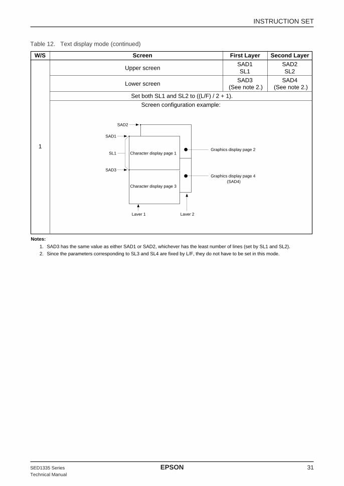
SED1335 Series EPSON 31Technical Manual
Table 12. Text display mode (continued)
W/S Screen First Layer Second Layer
Upper screenSAD1 SAD2SL1 SL2
Lower screenSAD3 SAD4
(See note 2.) (See note 2.)
Set both SL1 and SL2 to ((L/F) / 2 + 1).
Screen configuration example:
1
Notes:
1. SAD3 has the same value as either SAD1 or SAD2, whichever has the least number of lines (set by SL1 and SL2).
2. Since the parameters corresponding to SL3 and SL4 are fixed by L/F, they do not have to be set in this mode.
Character display page 1
Character display page 3
SAD2
SAD1
SAD3
SL1Graphics display page 2
Layer 2Layer 1
Graphics display page 4 (SAD4)
INSTRUCTION SET
32 EPSON SED1335 SeriesTechnical Manual
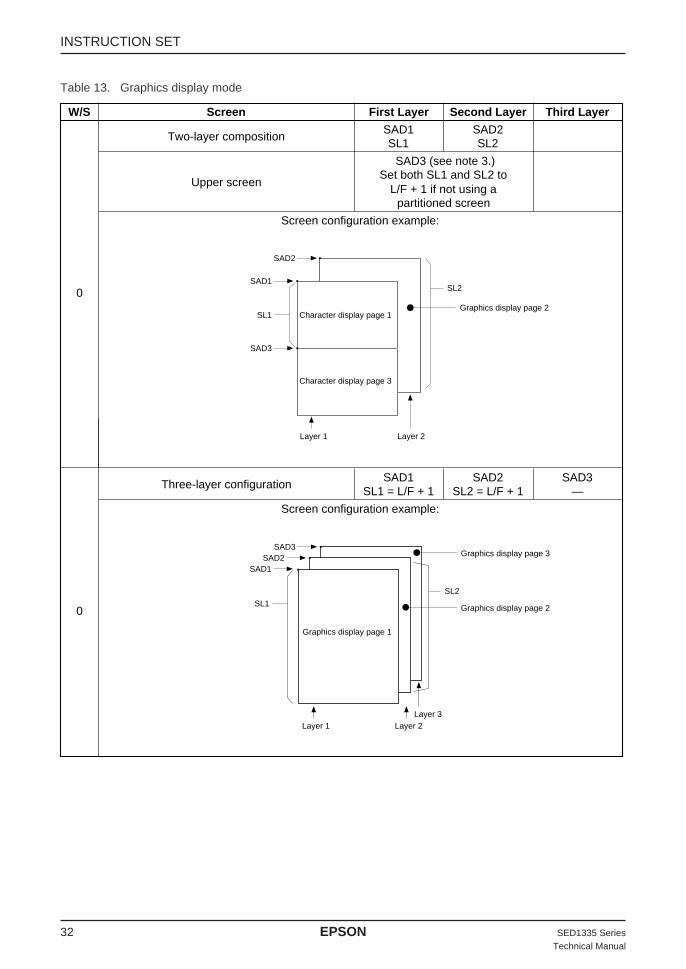
Table 13. Graphics display mode
W/S Screen First Layer Second Layer Third Layer
Two-layer compositionSAD1 SAD2SL1 SL2
SAD3 (see note 3.)
Upper screenSet both SL1 and SL2 to
L/F + 1 if not using apartitioned screen
Screen configuration example:
0
0
Three-layer configurationSAD1 SAD2 SAD3
SL1 = L/F + 1 SL2 = L/F + 1 —
Screen configuration example:
Character display page 1
Character display page 3
SAD2
SAD1
SAD3
SL1
SL2
Graphics display page 2
Layer 1 Layer 2
SAD2SAD1
SAD3
SL1
SL2
Graphics display page 2
Layer 1
Graphics display page 3
Layer 2Layer 3
Graphics display page 1
INSTRUCTION SET

SED1335 Series EPSON 33Technical Manual
Table 13. Graphics display mode (continued)
Notes:
1. SAD3 has the same value as either SAD1 or SAD2, whichever has the least number of lines (set by SL1 and SL2).
2. Since the parameters corresponding to SL3 and SL4 are fixed by L/F, they do not have to be set.
3. If, and only if, W/S = 1, the differences between SL1 and (L/F + 1) / 2, and between SL2 and (L/F + 1) / 2, are blanked.
W/S Screen First Layer Second Layer Third Layer
Upper screenSAD1 SAD2
—SL1 SL2
Lower screenSAD3 SAD4
—(See note 2.) (See note 2.)
Set both SL1 and SL2 to ((L/F) / 2 + 1).
Screen configuration example (See note 3.):
1Graphics display page 1
Graphics display page 3
SAD2
SAD1
SAD3
SL1Graphics display page 2
Layer 2Layer 1
Graphics display page 4
Upper Panel
Lower Panel
SL1
L/2
L
Graphics
Figure 12. Two-panel display height
INSTRUCTION SET

34 EPSON SED1335 SeriesTechnical Manual
8.3.3. CSRFORMSets the cursor size and shape. Although the cursor isnormally only used in text displays, it may also be used ingraphics displays when displaying special characters.
Figure 13. CSRFORM parameter bytes
8.3.3.1. CRX
Sets the horizontal size of the cursor from the characterorigin. CRX is equal to the cursor size less one. CRX mustbe less than or equal to FX.
Table 14. Horizontal cursor size selection
8.3.3.2. CRY
Sets the location of an underscored cursor in lines, fromthe character origin. When using a block cursor, CRY setsthe vertical size of the cursor from the character origin.CRY is equal to the number of lines less one.
Table 15. Cursor height selection
Figure 14. Cursor size and position
8.3.3.3. CM
Sets the cursor shape. Always set CM to 1 when ingraphics mode.CM = 0: Underscore cursorCM = 1: Block cursor
8.3.4. CSRDIRSets the direction of automatic cursor increment. Thecursor can move left or right one character, or up or downby the number of bytes specified by the address pitch, AP.When reading from and writing to display memory, thisautomatic cursor increment controls the display memoryaddress increment on each read or write.
Figure 15. CSRDIR parameters
Figure 16. Cursor direction
MSB LSB
C 0 1 0 1 1 1 0 1
P1 0 0 0 0 X3 X2CRX
X1 X0
P2 CM 0 0 0 Y3 Y2CRY
Y1 Y0
CRX [CRX] cursor widthHEX X3 X2 X1 X0 (pixels)
0 0 0 0 0 1
1 0 0 0 1 2
↓ ↓ ↓ ↓ ↓ ↓4 0 1 0 0 9
↓ ↓ ↓ ↓ ↓ ↓E 1 1 1 0 15
F 1 1 1 1 16
CRY [CRY] cursor heightHEX Y3 Y2 Y1 Y0 (lines)
0 0 0 0 0 Illegal
1 0 0 0 1 2
↓ ↓ ↓ ↓ ↓ ↓8 1 0 0 0 9
↓ ↓ ↓ ↓ ↓ ↓E 1 1 1 0 15
F 1 1 1 1 16
0 1 2 3 4 5 6 • • •0
1
2
3
4
5
6
7
8
9
Character start point
CRX = 5 dots
CRY = 9 dots
CM = 0
MSB LSB
C 0 1 0 0 1 1 CD1 CD2
10
11
0001–1 +1
+AP
–AP
INSTRUCTION SET
SED1335 Series EPSON 35Technical Manual
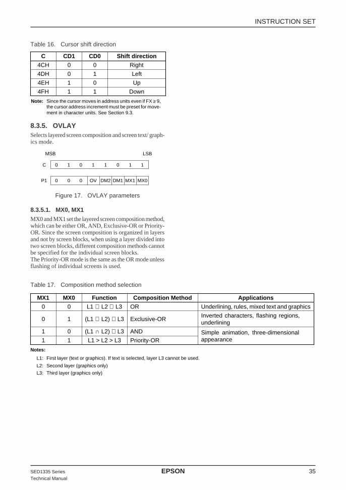
Table 16. Cursor shift direction
8.3.5. OVLAYSelects layered screen composition and screen text/ graph-ics mode.
Figure 17. OVLAY parameters
8.3.5.1. MX0, MX1
MX0 and MX1 set the layered screen composition method,which can be either OR, AND, Exclusive-OR or Priority-OR. Since the screen composition is organized in layersand not by screen blocks, when using a layer divided intotwo screen blocks, different composition methods cannotbe specified for the individual screen blocks.The Priority-OR mode is the same as the OR mode unlessflashing of individual screens is used.
C CD1 CD0 Shift direction
4CH 0 0 Right
4DH 0 1 Left
4EH 1 0 Up
4FH 1 1 Down
Note: Since the cursor moves in address units even if FX ≥ 9,the cursor address increment must be preset for move-ment in character units. See Section 9.3.
MSB LSB
C 0 1 0 1 1 0 1 1
P1 0 0 0 OV DM2 DM1 MX1 MX0
Table 17. Composition method selection
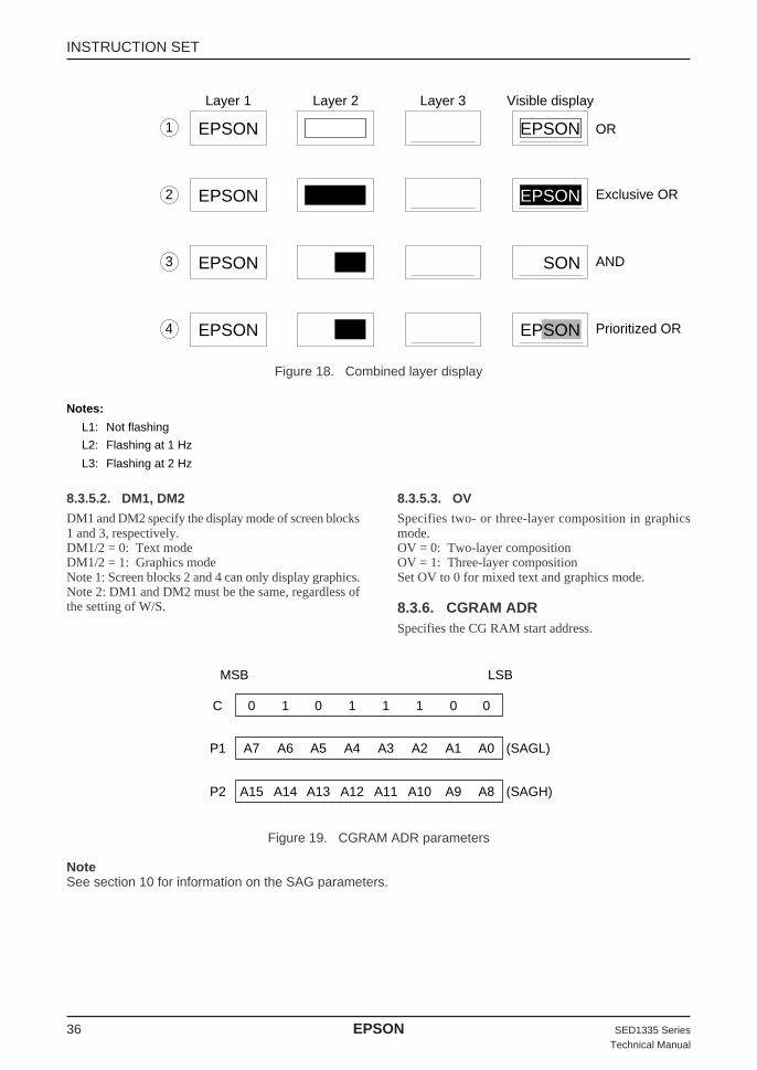
MX1 MX0 Function Composition Method Applications
0 0 L1 ∪ L2 ∪ L3 OR Underlining, rules, mixed text and graphics
0 1 (L1 ⊕ L2) ∪ L3 Exclusive-ORInverted characters, flashing regions, underlining
1 0 (L1 ∩ L2) ∪ L3 AND Simple animation, three-dimensional 1 1 L1 > L2 > L3 Priority-OR appearance
Notes:
L1: First layer (text or graphics). If text is selected, layer L3 cannot be used.
L2: Second layer (graphics only)
L3: Third layer (graphics only)
INSTRUCTION SET
36 EPSON SED1335 SeriesTechnical Manual
8.3.5.2. DM1, DM2
DM1 and DM2 specify the display mode of screen blocks1 and 3, respectively.DM1/2 = 0: Text modeDM1/2 = 1: Graphics modeNote 1: Screen blocks 2 and 4 can only display graphics.Note 2: DM1 and DM2 must be the same, regardless ofthe setting of W/S.
Figure 18. Combined layer display
Notes:
L1: Not flashing
L2: Flashing at 1 Hz
L3: Flashing at 2 Hz
EPSON
Layer 1 Layer 2 Layer 3
EPSON
Visible display
1 OR
EPSON2 Exclusive OR
EPSON3 AND
EPSON4 Prioritized OREPSON
SON
EPSON
8.3.5.3. OV
Specifies two- or three-layer composition in graphicsmode.OV = 0: Two-layer compositionOV = 1: Three-layer compositionSet OV to 0 for mixed text and graphics mode.
8.3.6. CGRAM ADRSpecifies the CG RAM start address.
MSB LSB
C 0 1 0 1 1 1 0 0
P1 A7 A6 A5 A4 A3 A2 A1 A0 (SAGL)
P2 A15 A14 A13 A12 A11 A10 A9 A8 (SAGH)
Figure 19. CGRAM ADR parameters
NoteSee section 10 for information on the SAG parameters.
INSTRUCTION SET

SED1335 Series EPSON 37Technical Manual
8.3.7. HDOT SCRWhile the SCROLL command only allows scrolling bycharacters, HDOT SCR allows the screen to be scrolledhorizontally by pixels. HDOT SCR cannot be used onindividual layers.
Figure 20. HDOT SCR parameters
8.3.7.1. D0 to D2
Specifies the number of pixels to scroll. The C/R param-eter has to be set to one more than the number ofhorizontal characters before using HDOT SCR. Smoothscrolling can be simulated if the controlling microproces-sor repeatedly issues the HDOT SCR command to theSED1335 series. See Section 9.5 for more information onscrolling the display.
Table 18. Scroll step selection (continued)
Figure 21. Horizontal scrolling
MSB LSB
C 0 1 0 1 1 0 1 0
P1 0 0 0 0 0 D2 D1 D0
P1 Number of pixelsHEX D2 D1 D0 to scroll
00 0 0 0 0
01 0 0 1 1
02 0 1 0 2
↓ ↓ ↓ ↓ ↓06 1 1 0 6
07 1 1 1 7
M
B X Y
A B X YZM = 0
N = 0
Display width N
M/N is the number of bits (dots) that parameter 1 (P1)is incremented/decremented by.
A
Z A B X Y
8.4. Drawing Control Commands8.4.1. CSRWThe 16-bit cursor address register contains the displaymemory address of the data at the cursor position asshown in Figure 22.Note that the microprocessor cannot directly access thedisplay memory.
The MREAD and MWRITE commands use the addressin this register.
MSB LSB
C 0 1 0 0 0 1 1 0
P1 A7 A6 A5 A4 A3 A2 A1 A0 (CSRL)
P2 A15 A14 A13 A12 A11 A10 A9 A8 (CSRH)
Figure 22. CSRW parameters
INSTRUCTION SET
38 EPSON SED1335 SeriesTechnical Manual
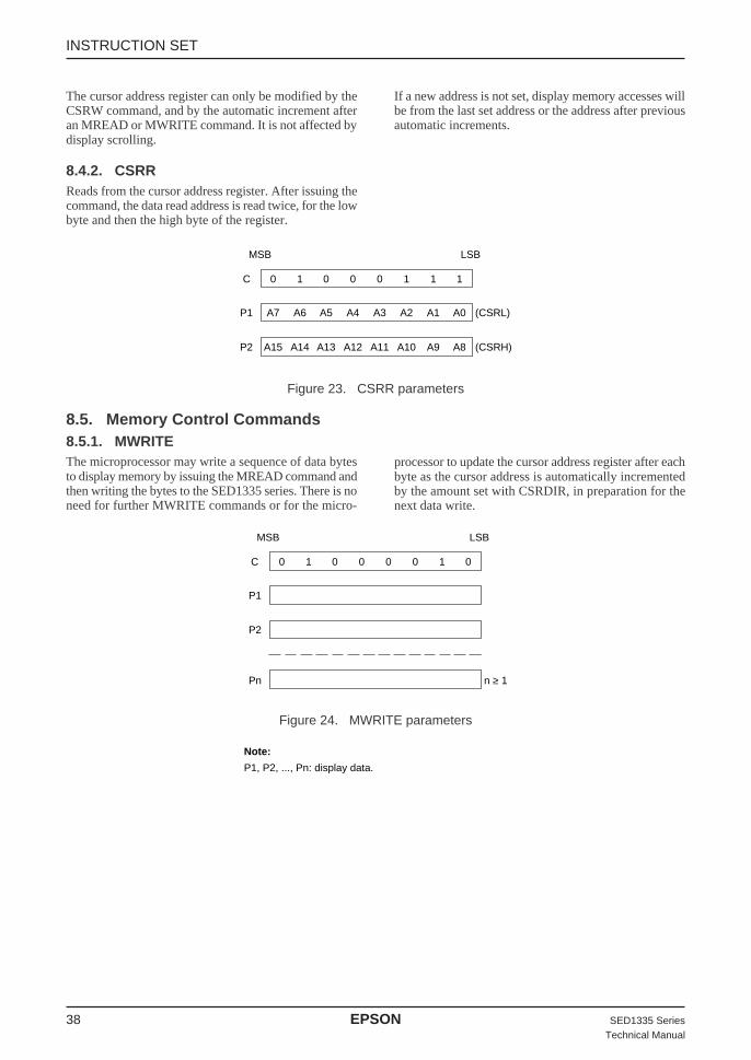
The cursor address register can only be modified by theCSRW command, and by the automatic increment afteran MREAD or MWRITE command. It is not affected bydisplay scrolling.
If a new address is not set, display memory accesses willbe from the last set address or the address after previousautomatic increments.
8.4.2. CSRRReads from the cursor address register. After issuing thecommand, the data read address is read twice, for the lowbyte and then the high byte of the register.
8.5. Memory Control Commands8.5.1. MWRITEThe microprocessor may write a sequence of data bytesto display memory by issuing the MREAD command andthen writing the bytes to the SED1335 series. There is noneed for further MWRITE commands or for the micro-
Figure 23. CSRR parameters
MSB LSB
C 0 1 0 0 0 1 1 1
P1 A7 A6 A5 A4 A3 A2 A1 A0 (CSRL)
P2 A15 A14 A13 A12 A11 A10 A9 A8 (CSRH)
processor to update the cursor address register after eachbyte as the cursor address is automatically incrementedby the amount set with CSRDIR, in preparation for thenext data write.
Figure 24. MWRITE parameters
MSB LSB
C 0 1 0 0 0 0 1 0
P1
P2
Pn n ≥ 1
Note:
P1, P2, ..., Pn: display data.
INSTRUCTION SET
SED1335 Series EPSON 39Technical Manual
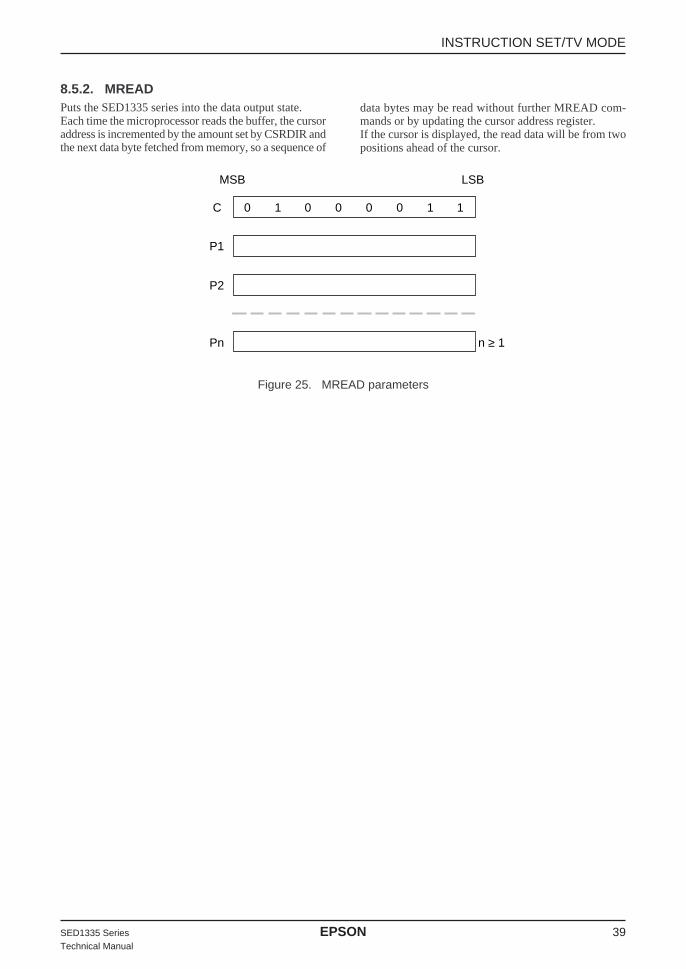
8.5.2. MREADPuts the SED1335 series into the data output state.Each time the microprocessor reads the buffer, the cursoraddress is incremented by the amount set by CSRDIR andthe next data byte fetched from memory, so a sequence of
data bytes may be read without further MREAD com-mands or by updating the cursor address register.If the cursor is displayed, the read data will be from twopositions ahead of the cursor.
MSB LSB
C 0 1 0 0 0 0 1 1
P1
P2
Pn n ≥ 1
Figure 25. MREAD parameters
INSTRUCTION SET/TV MODE
40 EPSON SED1335 SeriesTechnical Manual
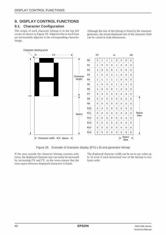
9. DISPLAY CONTROL FUNCTIONS9.1. Character ConfigurationThe origin of each character bitmap is in the top leftcorner as shown in Figure 29. Adjacent bits in each byteare horizontally adjacent in the corresponding characterimage.
Although the size of the bitmap is fixed by the charactergenerator, the actual displayed size of the character fieldcan be varied in both dimensions.
0
1
1
1
1
1
1
0
0
0
0
0
0
0
0
0
1
0
0
0
1
0
0
0
0
0
0
0
0
0
0
0
1
0
0
0
1
0
0
0
0
0
0
0
0
0
0
0
1
0
0
0
1
0
0
0
0
0
0
0
0
0
0
0
0
1
1
1
1
1
1
0
0
0
0
0
0
0
0
0
0
0
0
0
0
0
0
0
0
0
0
0
0
0
0
0
0
0
0
0
0
0
0
0
0
0
0
0
0
0
0
0
0
0
0
0
0
0
0
0
0
0
0
0
0
0
0
0
R0
R1
R2
R3
R4
R5
R6
R7
R8
R9
R10
R11
R12
R13
R14
R15
D7 to D0FX
Characterheight
Space
Character width Space
FY
Character starting point
Spacedata
Spacedata
Figure 26. Example of character display ([FX] ≤ 8) and generator bitmap
If the area outside the character bitmap contains onlyzeros, the displayed character size can easily be increasedby increasing FX and FY, as the zeros ensure that theextra space between displayed characters is blank.
The displayed character width can be set to any value upto 16 even if each horizontal row of the bitmap is twobytes wide.
DISPLAY CONTROL FUNCTIONS

SED1335 Series EPSON 41Technical Manual
Figure 27. Character width greater than one byte wide ([FX] = 9)
FY
Vertical non-display
area
CharacterHeight
Space
16 dots
Horizontalnon-display
areaFX
8 dots 8 dots
SpaceCharacter width
Note: The SED1335 series does not automatically insert spaces between characters. If the displayed character size is8 pixels or less and the space between character origins is nine pixels or more, the bitmap must use two bytes per row,even though the character image requires only one.
DISPLAY CONTROL FUNCTIONS
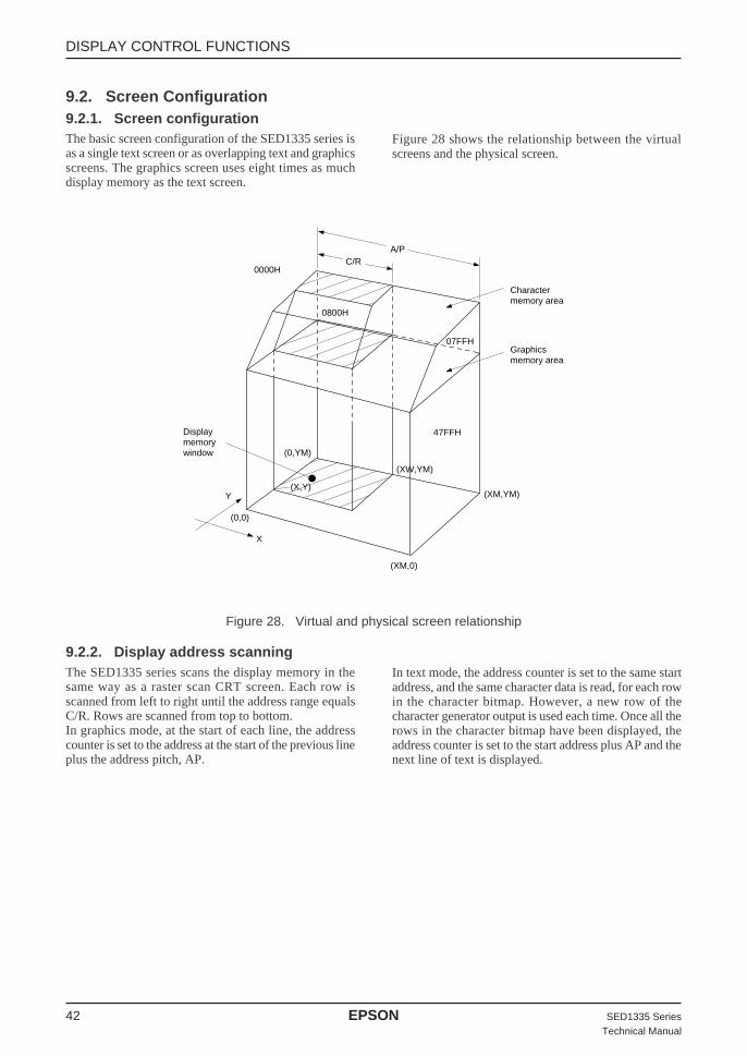
42 EPSON SED1335 SeriesTechnical Manual
9.2. Screen Configuration9.2.1. Screen configurationThe basic screen configuration of the SED1335 series isas a single text screen or as overlapping text and graphicsscreens. The graphics screen uses eight times as muchdisplay memory as the text screen.
Figure 28 shows the relationship between the virtualscreens and the physical screen.
9.2.2. Display address scanningThe SED1335 series scans the display memory in thesame way as a raster scan CRT screen. Each row isscanned from left to right until the address range equalsC/R. Rows are scanned from top to bottom.In graphics mode, at the start of each line, the addresscounter is set to the address at the start of the previous lineplus the address pitch, AP.
In text mode, the address counter is set to the same startaddress, and the same character data is read, for each rowin the character bitmap. However, a new row of thecharacter generator output is used each time. Once all therows in the character bitmap have been displayed, theaddress counter is set to the start address plus AP and thenext line of text is displayed.
Figure 28. Virtual and physical screen relationship
A/P
Character memory area
Graphics memory area
(XM,YM)
(XM,0)
(0,0)
(X,Y)
(0,YM)
(XW,YM)
0800H
0000H
Display memory window
07FFH
47FFH
C/R
Y
X
DISPLAY CONTROL FUNCTIONS

SED1335 Series EPSON 43Technical Manual
Figure 29. Character position parameters
Figure 30. Character parameters vs. memory
W/S = 0, FX = 8, FY = 8
C/R
1•••89•••1617•••24••••
SAD
SAD + AP
SAD + 2AP
SAD + 1
SAD + AP + 1
SAD + 2
SAD + AP + 2
SAD + C/R
SAD + AP + C/R
Note: One byte of display memory corresponds to one character.
SAD
SAD + AP
SAD + 2AP
SAD +1
SAD + AP + 1
SAD + 2
SAD + AP + 2
SAD + C/R
SAD + AP + C/R
1
2
3
••••••••
W/S = 0, FX = 8
C/R
SADSAD +1SAD + 2
SAD + C/R
SAD + APSAD + AP + 1
SAD + AP + C/R
SAD + 2AP
Line 1
Line 2
Line 3
AP
AP
Note: One bit of display memory corresponds to one pixel.
DISPLAY CONTROL FUNCTIONS
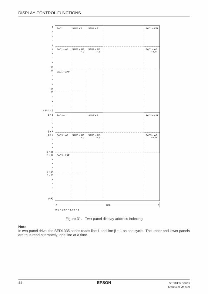
44 EPSON SED1335 SeriesTechnical Manual
Figure 31. Two-panel display address indexing
NoteIn two-panel drive, the SED1335 series reads line 1 and line β + 1 as one cycle. The upper and lower panelsare thus read alternately, one line at a time.
SAD1 SAD1 + 1 SAD1 + 2 SAD1 + C/R
SAD1 + AP SAD1 + AP + 1
SAD1 + AP + 2
SAD1 + AP + C/R
SAD1 + 2AP
SAD3 + 1 SAD3 + 2 SAD3 + C/R
SAD3 + AP SAD3 + AP + 1
SAD3 + AP + 2
SAD3 + AP + C/R
SAD3 + 2AP
1
•
•
•
8
9
•
•
•
16
17
•
•
•
24
25
•
•
•
(L/F)/2 = β
β + 1
•
•
•
β + 8
β + 9
•
•
•
β + 16
β + 17
•
•
•
β + 24
β + 25
•
•
•
•
(L/F)
W/S = 1, FX = 8, FY = 8
C/R
DISPLAY CONTROL FUNCTIONS
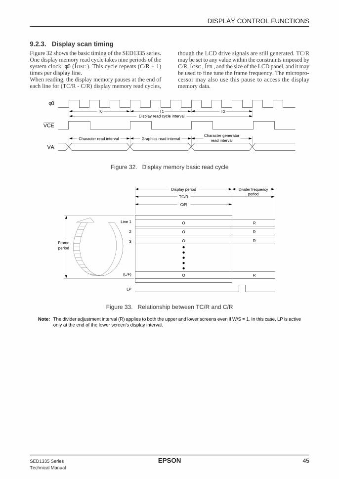
SED1335 Series EPSON 45Technical Manual
9.2.3. Display scan timingFigure 32 shows the basic timing of the SED1335 series.One display memory read cycle takes nine periods of thesystem clock, φ0 (fOSC ). This cycle repeats (C/R + 1)times per display line.When reading, the display memory pauses at the end ofeach line for (TC/R - C/R) display memory read cycles,
though the LCD drive signals are still generated. TC/Rmay be set to any value within the constraints imposed byC/R, fOSC , fFR , and the size of the LCD panel, and it maybe used to fine tune the frame frequency. The micropro-cessor may also use this pause to access the displaymemory data.
Figure 32. Display memory basic read cycle
T0 T1 T2Display read cycle interval
Graphics read intervalCharacter read intervalCharacter generator
read interval
φ0
VCE
VA
Figure 33. Relationship between TC/R and C/R
Frameperiod
Display period Divider frequencyperiod
TC/R
C/R
O
O
O
•••••O
R
R
R
R
Line 1
2
3
(L/F)
LP
Note: The divider adjustment interval (R) applies to both the upper and lower screens even if W/S = 1. In this case, LP is activeonly at the end of the lower screen’s display interval.
DISPLAY CONTROL FUNCTIONS

46 EPSON SED1335 SeriesTechnical Manual
9.3. Cursor Control9.3.1. Cursor register functionThe SED1335 series cursor address register functions asboth the displayed cursor position address register andthe display memory access address register. When ac-cessing display memory outside the actual screen memory,the address register must be saved before accessing thememory and restored after memory access is complete.
Figure 34. Cursor addressing
Note that the cursor may disappear from the display if thecursor address remains outside the displayed screenmemory for more than a few hundred milliseconds.
9.3.2. Cursor movementOn each memory access, the cursor address registerchanges by the amount previously specified with CSRDIR,automatically moving the cursor to the desired location.
9.3.3. Cursor display layersAlthough the SED1335 series can display up to threelayers, the cursor is displayed in only one of these layers:Two-layer configuration: First layer (L1)Three-layer configuration: Third layer (L3)The cursor will not be displayed if it is moved outside thememory for its layer. Layers may be swapped or thecursor layer moved within the display memory if it isnecessary to display the cursor on a layer other than thepresent cursor layer.
Cursor displayaddress register
Address pointer
Cursor register
Although the cursor is normally displayed for characterdata, the SED1335 series may also display a dummycursor for graphical characters. This is only possible if thegraphics screen is displayed, the text screen is turned offand the microprocessor generates the cursor control ad-dress.
Figure 35. Cursor display layers
Consider the example of displaying Chinese characterson a graphics screen. To write the display data, the cursoraddress is set to the second screen block, but the cursor isnot displayed. To display the cursor, the cursor address isset to an address within the blank text screen block.Since the automatic cursor increment is in address units,not character units, the controlling microprocessor mustset the cursor address register when moving the cursorover the graphical characters.
D = 1
FC1 = 0
FC0 = 1
FP1 = 0
FP0 = 0
FP3 = 0
FP2 = 1
Cursor ON
Block screen 1 (characterscreen) OFF
Block screen 2 (graphicsscreen) ON
DISPLAY CONTROL FUNCTIONS

SED1335 Series EPSON 47Technical Manual
If no text screen is displayed, only a bar cursor can bedisplayed at the cursor address.If the first layer is a mixed text and graphics screen and thecursor shape is set to a block cursor, the SED1335 series
automatically decides which cursor shape to display. Onthe text screen it displays a block cursor, and on thegraphics screen, a bar cursor.
Figure 36. Cursor movement
18 dots
Auto shift Auto shift
Auto shift
Cursor address preset
8 dots8 dots8 dots8 dotsBlock cursor
DISPLAY CONTROL FUNCTIONS
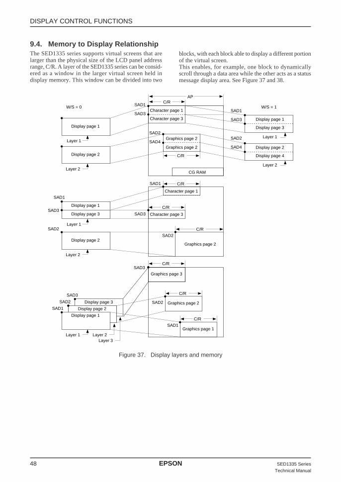
48 EPSON SED1335 SeriesTechnical Manual
9.4. Memory to Display RelationshipThe SED1335 series supports virtual screens that arelarger than the physical size of the LCD panel addressrange, C/R. A layer of the SED1335 series can be consid-ered as a window in the larger virtual screen held indisplay memory. This window can be divided into two
blocks, with each block able to display a different portionof the virtual screen.This enables, for example, one block to dynamicallyscroll through a data area while the other acts as a statusmessage display area. See Figure 37 and 38.
Figure 37. Display layers and memory
Graphics page 3
Display page 3
Display page 2
Display page 1
Character page 1
Character page 3 Display page 1
Display page 3
Layer 1Layer 1
Display page 2
Graphics page 2
Graphics page 2 Display page 2
Display page 4
Layer 2Layer 2
SAD1
SAD3
SAD2
SAD4
SAD1
SAD3
SAD2
SAD4
APC/R
W/S = 0 W/S = 1
C/R
CG RAM
Display page 1
Character page 1
Character page 3
Layer 1
Display page 2
Layer 2
SAD1
Graphics page 2
SAD2
SAD3SAD3Display page 3
SAD2
SAD1 C/R
C/R
C/R
Display page 1
Layer 1
Graphics page 2
Graphics page 1Layer 2
Layer 3
SAD1
SAD2
SAD3
SAD3
SAD2
SAD1
C/R
C/R
C/R
DISPLAY CONTROL FUNCTIONS

SED1335 Series EPSON 49Technical Manual
Figure 38. Display window and memory
AP
CSRA CRX
CRY
FXSAD1
FY
L/F
Displaywindow
C/R
Virtual displaymemory limit
0000H
FFFFH
FX = Horizontal character field ≤ 16 dots
FY = Vertical character field ≤ 16 dots
CRX = Horizontal cursor size ≤ 16 dots
CRY = Vertical cursor size ≤ 16 dots
C/R = Characters per row ≤ 240 bytes
L/F = Lines per frame ≤ 256 bytes
AP = Address pitch ≤ 64 Kbytes
DISPLAY CONTROL FUNCTIONS
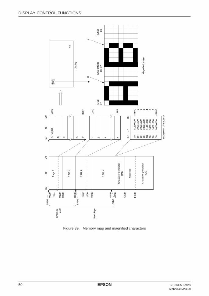
50 EPSON SED1335 SeriesTechnical Manual
Figure 39. Memory map and magnified characters
SA
D1
SA
D2
SA
G
0000
SL1
0300
0400
0800
SL2
2000
2800
4440
4800
4A00
F00
0
Cha
ract
erco
de
Bac
k la
yer
Pag
e 1
Pag
e 2
Pag
e 1
Pag
e 2
Cha
ract
er g
ener
ator
RA
M
Not
use
d
Cha
ract
er g
ener
ator
RO
M
D7
toD
0D
7to
D0
A (
Cod
e)
B C X Y α β γ χ 70 88 88 88 F8
88 88 00
0111
0000
1000
1000
1000
1000
1000
1000
1111
1000
1000
1000
1000
1000
0000
0000
HE
XD
7D
0
Exa
mpl
e of
cha
ract
er A
#480
0 1 2 3 4 5 6#4
807
0080
1FF
F
0000
02F
F
(MS
B)
D7
(LS
B)(
MS
B)
D0
D7
Mag
nifie
d im
age
(LS
B)
D0
βα
Dis
play
XY
AB
C
DISPLAY CONTROL FUNCTIONS

SED1335 Series EPSON 51Technical Manual
9.5. ScrollingThe controlling microprocessor can set the SED1335series scrolling modes by overwriting the scroll addressregisters SAD1 to SAD4, and by directly setting thescrolling mode and scrolling rate.
9.5.1. On-page scrollingThe normal method of scrolling within a page is to movethe whole display up one line and erase the bottom line.
Since the SED1335 series does not automatically erasethe bottom line, it must be erased with blanking data whenchanging the scroll address register.
9.5.2. Inter-page scrollingScrolling between pages and page switching can beperformed only if the display memory capacity is greaterthan one screen.
Figure 40. On-page scrolling
ABC
WXYZ 789
WXYZ 789
ABC
WXYZ 789
WXYZ 789
Display memory
AP
C/R
Before scrolling
After scrolling
Blank
Blank
SAD1
SAD3
SAD1
Figure 41. Inter-page scrolling
ABC
WXYZ 789
WXYZ 789
ABC
WXYZ 789
WXYZ 789
Display memory
AP
C/R
Before scrolling
After scrolling
SAD1
SAD1ABC
DISPLAY CONTROL FUNCTIONS

52 EPSON SED1335 SeriesTechnical Manual
9.5.3. Horizontal scrollingThe display can be scrolled horizontally in one-characterunits, regardless of the display memory capacity.
Figure 42. Horizontal wraparound scrolling
ABC123
XYZ
BC23
XYZ1
Before scrolling
After scrolling
SAD1
SAD1
Display
AP
C/R
Display memory
ABC123
XYZ
ABC123
XYZ
DISPLAY CONTROL FUNCTIONS

SED1335 Series EPSON 53Technical Manual
9.5.4. Bidirectional scrollingBidirectional scrolling can be performed only if thedisplay memory is larger than the physical screen bothhorizontally and vertically. Although scrolling is nor-mally done in single-character units, the HDOT SCR
command can be used to scroll horizontally in pixel units.Single-pixel scrolling both horizontally and verticallycan be performed by using the SCROLL and HDOT SCRcommands. See Section 16.4
Figure 43. Bidirectional scrolling
BC EFG TUV
12
Before scrolling
After scrolling
Display memory
FGTUV
123456
BC EFG TUV
A
34567 89
12
ABC E FG TUV
56 7 89
1234
AP
C/R
9.5.5. Scroll unitsTale 19. Scroll units
Mode Vertical Horizontal
Text CharactersPixels orcharacters
Graphics Pixels Pixels
Note that in a divided screen, each block cannot be indepen-dently scrolled horizontally in pixel units.
DISPLAY CONTROL FUNCTIONS

54 EPSON SED1335 SeriesTechnical Manual
10. CHARACTER GENERATOR10.1. CG Characteristics10.1.1. Internal character generatorThe internal character generator is recommended forminimum system configurations containing a SED1335series, display RAM, LCD panel, single-chip micropro-cessor and power supply. Since the internal charactergenerator uses a CMOS mask ROM, it is also recom-mended for low-power applications.• 5 × 7-pixel font (See Section 17.)• 160 JIS standard characters• Can be mixed with character generator RAM (maxi-
mum of 64 CG RAM characters)• Can be automatically spaced out up to 8 × 16 pixels
10.1.2. External character generator ROMThe external CG ROM can be used when fonts other thanthose in the internal ROM are needed. Data is stored in theexternal ROM in the same format used in the internalROM. (See Section 10.3.)• Up to 8 × 8-pixel characters (M2 = 0) or 8 × 16-pixel
characters (M2 = 1)• Up to 256 characters (192 if used together with the
internal ROM)• Mapped into the display memory address space at
F000H to F7FFH (M2 = 0) or F000H to FFFFH (M2= 1)
• Characters can be up to 8 × 16-pixels; however, excessbits must be set to zero.
10.1.3. Character generator RAMThe user can freely use the character generator RAM forstoring graphics characters. The character generator RAMcan be mapped by the microprocessor anywhere in dis-play memory, allowing effective use of unused addressspace.• Up to 8 × 8-pixel characters (M2 = 0) or 8 × 16
characters (M2 = 1)• Up to 256 characters if mapped at F000H to FFFFH
(64 if used together with character generator ROM)• Can be mapped anywhere in display memory address
space if used with the character generator ROM• Mapped into the display memory address space at
F000H to F7FFH if not used with the character gen-erator ROM (more than 64 characters are in the CGRAM). Set SAG0 to F000H and M1 to zero whendefining characters number 193 upwards.
CHARACTER GENERATOR

SED1335 Series EPSON 55Technical Manual
10.2. CG Memory AllocationSince the SED1335 series uses 8-bit character codes, itcan handle no more than 256 characters at a time. How-ever, if a wider range of characters is required, character
generator memory can be bank-switched using theCGRAM ADR command.
Figure 44. Internal and external character mapping
Note that there can be no more than 64 characters per bank.
Built–in CG ROM(160 characters,
5 × 7 pixels max)
CG RAM CG RAM 1
CG RAM 2CG RAM n
Built-in CG ROM(160 characters,
5 × 7 pixels max)
CG RAM CG RAM 1
CG RAM 2CG RAM n
SAG
CG RAMADR
CG ROM
CG RAM
(64 characters max, 8 × 16 pixels max)
(64 characters max, 8 × 16 pixels max)
M0 = 1
M0 = 1
Basic CG space(256 characters,
8 × 16 pixels max) 256 characters maxM1 = 0
256 characters maxM1 = 0
Table 20. Character mapping
Item Parameter Remarks
Internal/external character generator selection M0
1 to 8 pixels M2 = 0
Character field height 9 to 16 pixels M2 = 1
Greater than 16 pixels Graphics mode (8 bits × 1 line)
Internal CG ROM/RAM selectAutomatic
Determined by theExternal CG ROM/RAM select character code
CG RAM bit 6 correction M1
CG RAM data storage addressSpecified with CG RAM ADR Can be moved anywhere in thecommand display memory address space
192 characters or less Other than the area of Figure 49
More than 192 charactersSet SAG to F000H and overlySAG and the CG ROM table
External CG ROMaddress
CHARACTER GENERATOR

56 EPSON SED1335 SeriesTechnical Manual
10.3. Setting the Character Generator Addresscalculated from SAG + character code + ROW selectaddress. This mapping is shown in Table 21 and 22.
Table 21. Character fonts, number of lines ≤ 8 (M2 = 0, M1 = 0)
Table 22. Character fonts, 9 ≤ number of lines ≤ 16 (M2 = 1, M1 = 0)
SAG A15 A14 A13 A12 A11 A10 A9 A8 A7 A6 A5 A4 A3 A2 A1 A0
Character code 0 0 0 0 D7 D6 D5 D4 D3 D2 D1 D0 0 0 0 0
+ROW select address 0 0 0 0 0 0 0 0 0 0 0 0 R3 R2 R1 R0
CG RAM address VA15 VA14 VA13 VA12 VA11 VA10 VA9 VA8 VA7 VA6 VA5 VA4 VA3 VA2 VA1 VA0
SAG A15 A14 A13 A12 A11 A10 A9 A8 A7 A6 A5 A4 A3 A2 A1 A0
Character code 0 0 0 0 0 D7 D6 D5 D4 D3 D2 D1 D0 0 0 0
+ROW select address 0 0 0 0 0 0 0 0 0 0 0 0 0 R2 R1 R0
CG RAM address VA15 VA14 VA13 VA12 VA11 VA10 VA9 VA8 VA7 VA6 VA5 VA4 VA3 VA2 VA1 VA0
Figure 45. Row select address
10.3.1. M1 = 1The SED1335 series automatically converts all bits set inbit 6 of character code for CG RAM 2 to zero. Because ofthis, the CG RAM data areas become contiguous indisplay memory.
Row
Row 0
Row 1
Row 2
Row 7
Row 8
Row 14
Row 15
R3
0
0
0
0
1
1
1
R2
0
0
0
1
0
1
1
R1
0
0
1
1
0
1
1
R0
0
1
0
1
0
0
1
Line 1
Line 2
Note: Lines = 1: lines in the character bitmap ≤ 8
Lines = 2: lines in the character bitmap ≥ 9
The CG RAM addresses in the VRAM address space arenot mapped directly from the address in the SAG register.The data to be displayed is at a CG RAM address
When writing data to CG RAM:• Calculate the address as for M1 = 0.• Change bit 6 of the character code from “1” to “0”.
CHARACTER GENERATOR

SED1335 Series EPSON 57Technical Manual
10.3.2. CG RAM addressing example• Define a pattern for the “A” in Figure 26.• The CG RAM table start address is 4800H.• The character code for the defined pattern is 80H (the
first character code in the CG RAM area).As the character code table in Figure 46 shows, codes80H to 9FH and E0H to FFH are allocated to the CG RAM
and can be used as desired. 80H is thus the first code forCG RAM. As characters cannot be used if only usinggraphics mode, there is no need to set the CG RAM data.
Table 23. Character data example
CGRAM AD
P1
P2
CSRDIR
CSRW
P1
P2
MWRITE
P
P2
P3
P4
P5
P6
P7
P8
P8
↓P16
5CH
00H
40H
4CH
46H
00H
48H
42H
70H
88H
88H
88H
F8H
88H
88H
00H
00H
↓00H
Reverse the CG RAM address calculation to calculate SAG
Set cursor shift direction to right
CG RAM start address is 4800H
Write ROW 0 data
Write ROW 1 data
Write ROW 2 data
Write ROW 3 data
Write ROW 4 data
Write ROW 5 data
Write ROW 6 data
Write ROW 7 data
Write ROW 8 data
↓Write ROW 15 data
CHARACTER GENERATOR

58 EPSON SED1335 SeriesTechnical Manual
10.4. Character CodesThe following figure shows the character codes and thecodes allocated to CG RAM. All codes can be used by theCG RAM if not using the internal ROM.
Figure 46. On-chip character codes
0Lower 4 bits
CG RAM1
M1 = 0
M1 = 1
CG RAM2
0
1
2
3
4
5
6
7
8
9
A
B
C
D
E
F
1 2
!
"
#
$
%
&
'
(
)
*
+
,
.
-
/
3
0
1
2
3
4
5
6
7
8
9
:
;
<
=
>
?
4
@
A
B
C
D
E
F
G
H
I
J
K
L
M
N
O
5
P
Q
R
S
T
U
V
W
X
Y
Z
[
¥
]
^
_
6
'
a
b
c
d
e
f
g
h
i
j
k
l
m
n
o
7
p
q
r
s
t
u
v
w
x
y
z
|
→
←
8
Upper 4 bits
9 A B C D E F
CHARACTER GENERATOR
SED1335 Series EPSON 59Technical Manual
11. MICROPROCESSOR INTERFACE11.1. System Bus InterfaceSEL1, SEL2, A0, RD, WR and CS are used as controlsignals for the microprocessor data bus. A0 is normallyconnected to the lowest bit of the system address bus.SEL1 and SEL2 change the operation of the RD and WRpins to enable interfacing to either an 8080 or 6800 familybus, and should have a pull-up or pull-down resistor.With microprocessors using an 8080 family interface, theSED1335 series is normally mapped into the I/O addressspace.
11.1.1. 8080 seriesTable 24. 8080 series interface signals
11.1.2. 6800 seriesTable 25. 6800 series interface signals
11.2. Microprocessor SynchronizationThe SED1335 series interface operates at full bus speed,completing the execution of each command within thecycle time, tCYC . The controlling microprocessor’s per-formance is thus not hampered by polling or handshakingwhen accessing the SED1335 series.
Display flicker may occur if there is more than oneconsecutive access that cannot be ignored within a frame.The microprocessor can minimize this either by perform-ing these accesses intermittently, or by continuouslychecking the status flag (D6) and waiting for it to becomeHIGH.
11.2.1. Display status indication outputWhen CS, A0 and RD are LOW, D6 functions as thedisplay status indication output. It is HIGH during theTV-mode vertical retrace period or the LCD-mode hori-zontal retrace period, and LOW, during the period thecontroller is writing to the display. By monitoring D6 andwriting to the data memory only during retrace periods,the display can be updated without causing screen flicker.
11.2.2. Internal register accessThe SYSTEM SET and SLEEP IN commands can beused to perform input/output to the SED1335 seriesindependently of the system clock frequency. These arethe only commands that can be used while the SED1335series is in sleep mode.
11.2.3. Display memory accessThe SED1335 series supports a form of pipelined pro-cessing, in which the microprocessor synchronizes itsprocessing to the SED1335 series timing. When writing,the microprocessor first issues the MWRITE command.It then repeatedly writes display data to the SED1335series using the system bus timing. This ensures that themicroprocessor is not slowed down even if the displaymemory access times are slower than the system busaccess times. See Figure 47.When reading, the microprocessor first issues the MREADcommand, which causes the SED1335 series to load thefirst read data into its output buffer. The microprocessorthen reads data from the SED1335 series using the systembus timing. With each read, the SED1335 series reads thenext data item from the display memory ready for the nextread access. See Figure 48.
A0 RD WR Function
0 0 1 Status flag read
1 0 1Display data and cursor addressread
0 1 0 Display data and parameter write
1 1 0 Command write
0 1 1 Status flag read
1 1 1Display data and cursor addressread
0 0 1 Display data and parameter write
1 0 1 Command write
FunctionER/WA0
MICROPROCESSOR INTERFACE

60 EPSON SED1335 SeriesTechnical Manual
Figure 47. Display memory write cycle
Figure 48. Display memory read cycle
NoteA possible problem with the display memory read cycle is that the system bus access time, tACC, does notdepend on the display memory access time, tACV. The microprocessor may only make repeated reads if theread loop time exceeds the SED1335 series cycle time, tCYC. If it does not, NOP instructions may be insertedin the program loop. tACC, tACV and tCYC limits are given in section 6.2.
WR
D0 to D7
VR/W
VD0 to VD7
tCYC
Command write Data write Data writeMicroprocessor
Display memoryVRW
tCYCCommand write
Data read Data read
WR
RD
D0 to D7
VR/W
VD0 to VD7
Microprocessor
Display memoryVRW
MICROPROCESSOR INTERFACE
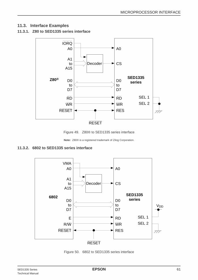
SED1335 Series EPSON 61Technical Manual
11.3. Interface Examples11.3.1. Z80 to SED1335 series interface
Figure 49. Z80® to SED1335 series interface
Note: Z80® is a registered trademark of Zilog Corporation.
11.3.2. 6802 to SED1335 series interface
RESET
Z80®
Decoder
IORQ
SED1335series
SEL 1
SEL 2
A0
A1to
A15
D0to
D7
RD
WR
RESET
A0
CS
D0toD7
RD
WR
RES
Figure 50. 6802 to SED1335 series interface
RESET
6802
Decoder
A0
CS
D0toD7
RD
WR
RES
VMA
VDD
SED1335series
SEL 1
SEL 2
A0
A1to
A15
D0to
D7
E
R/W
RESET
MICROPROCESSOR INTERFACE
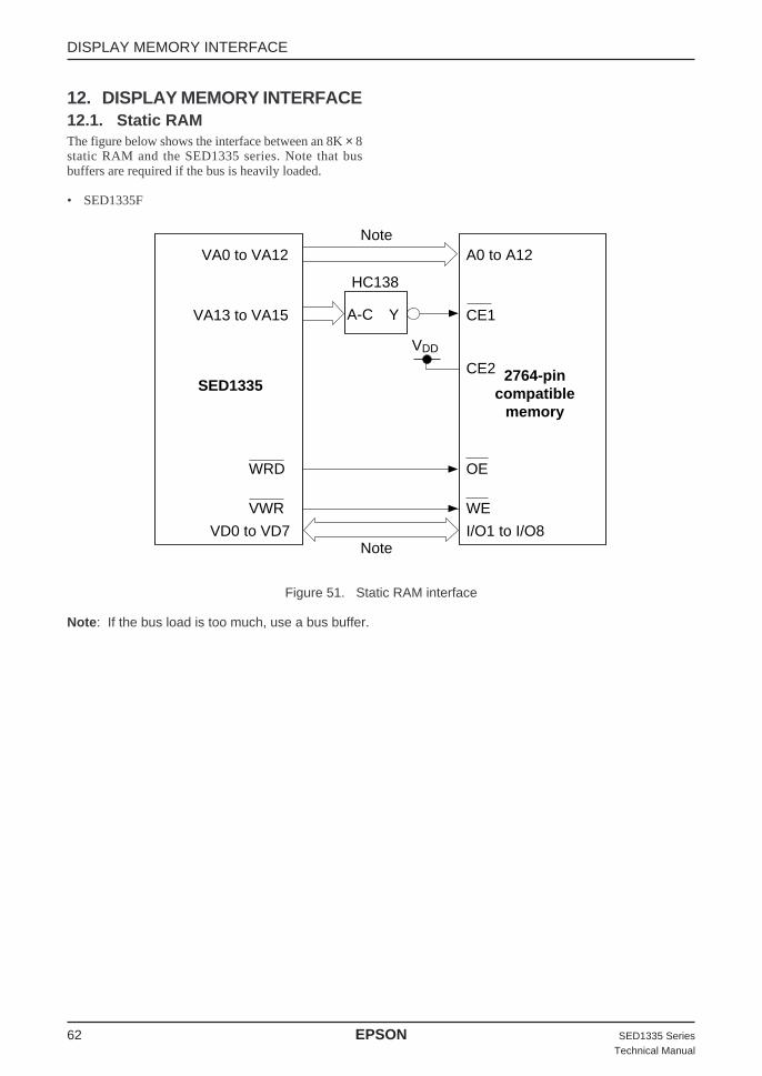
62 EPSON SED1335 SeriesTechnical Manual
12. DISPLAY MEMORY INTERFACE12.1. Static RAMThe figure below shows the interface between an 8K × 8static RAM and the SED1335 series. Note that busbuffers are required if the bus is heavily loaded.
• SED1335F
Figure 51. Static RAM interface
Note : If the bus load is too much, use a bus buffer.
HC138
Note
Note
VDD
SED13352764-pin
compatiblememory
A0 to A12
CE1
CE2
WE
I/O1 to I/O8
VA0 to VA12
VA13 to VA15
VWR
VD0 to VD7
OEWRD
YA-C
DISPLAY MEMORY INTERFACE

SED1335 Series EPSON 63Technical Manual
12.2. Supply Current during Display Memory AccessThe 24 address and data lines of the SED1335 series cycleat one-third of the oscillator frequency, fOSC. The chargeand discharge current on these pins, IVOP, is given by theequation below. When IVOP exceeds IOPR, it can beestimated by:
IVOP ∝ C V f
where C is the capacitance of the display memory bus, Vis the operating voltage, and f is the operating frequency.
If V OPR = 5.0V, f = 1.0 MHz, and the display memory buscapacitance is 1.0 pF per line:
IVOP ≤ 120 µA / MHz × pF
To reduce current flow during display memory accesses,it is important to use low-power memory, and to mini-mize both the number of devices and the parasitic capaci-tance.
13. OSCILLATOR CIRCUITThe SED1335 series incorporates an oscillator circuit. Astable oscillator can be constructed simply by connectingan AT-cut crystal and two capacitors to XG and XD, asshown in the figure below. If the oscillator frequency isincreased, CD and CG should be decreased proportion-ally.Note that the circuit board lines to XG and XD must be asshort as possible to prevent wiring capacitance fromchanging the oscillator frequency or increasing the powerconsumption.
Figure 52. Crystal oscillator
SED1335 series
XDXG
CDCG
CD = 3 to 20 pF
CG = 2 to 18 pF
Load impedance = 700 Ω (max)
14. STATUS FLAGThe SED1335 series has a single bit status flag.D6: X line standby
Figure 53. Status flag
The D6 status flag is HIGH for the TC/R-C/R cycles at theend of each line where the SED1335 series is not readingthe display memory. The microprocessor may use thisperiod to update display memory without affecting thedisplay, however it is recommended that the display beturned off when refreshing the whole display.
D7 D0
X D6 X X X X X X X: Don’t care
Figure 54. C/R to TC/R time difference
tm
tTC/R
LP
XSCL
tC/R
CS A0 RD D6 (flag)
0 0 0 0: Period of retrace lines1: Period of display
DISPLAY MEMORY INTERFACE/OSCILLATOR CIRCUIT/STATUS FLAG

64 EPSON SED1335 SeriesTechnical Manual
Figure 55. Flowchart for busy flag checking
Read Status Flag
D6 = 0?
Data Input
Data Input ?
No
No
Yes
Yes
STATUS FLAG
<Timing To Be Observed For Avoiding SED 1330 Series Write Noise>
• Precaution on the write timing to VRAM
LP
XSCL
5 × 9 × tOSC Display memory write time2 × 9 × tOSC
The allowable writing duration is since “5 × 9 × tOSC” has elapsed (tOSC = 1/fOSC: a cycle of theoscillation frequency) from the positive going edge of LP up to (TCR) – (C/R) – 7 × 9 × tOSC.
Currently employed D6 status flag reading method doesnot identify the timing when the read D6 = Low tookplace. Thus, negative going edge of LP should be used asthe interrupt signal when implementing the writing in
above timing.If you try to access the display memory in other timingthan the above, flickering of the display screen will result.
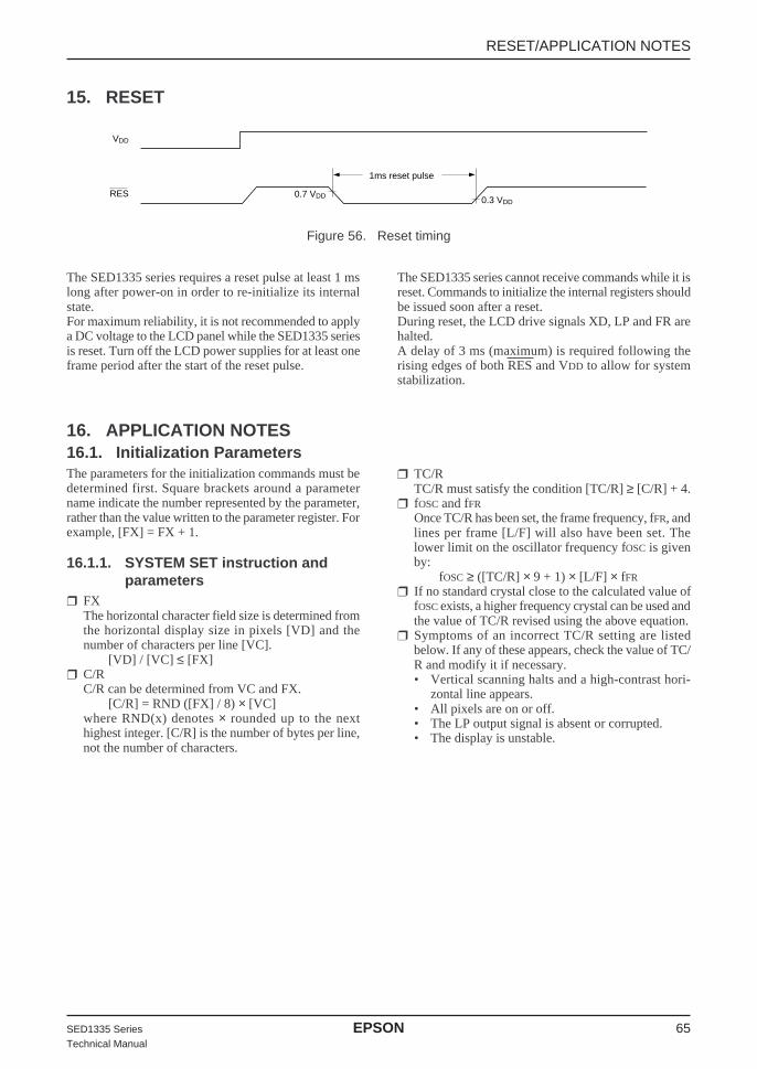
SED1335 Series EPSON 65Technical Manual
16. APPLICATION NOTES16.1. Initialization ParametersThe parameters for the initialization commands must bedetermined first. Square brackets around a parametername indicate the number represented by the parameter,rather than the value written to the parameter register. Forexample, [FX] = FX + 1.
16.1.1. SYSTEM SET instruction andparameters
FXThe horizontal character field size is determined fromthe horizontal display size in pixels [VD] and thenumber of characters per line [VC].
[VD] / [VC] ≤ [FX] C/R
C/R can be determined from VC and FX.[C/R] = RND ([FX] / 8) × [VC]
where RND(x) denotes × rounded up to the nexthighest integer. [C/R] is the number of bytes per line,not the number of characters.
TC/RTC/R must satisfy the condition [TC/R] ≥ [C/R] + 4.
fOSC and fFR
Once TC/R has been set, the frame frequency, fFR, andlines per frame [L/F] will also have been set. Thelower limit on the oscillator frequency fOSC is givenby:
fOSC ≥ ([TC/R] × 9 + 1) × [L/F] × fFR
If no standard crystal close to the calculated value offOSC exists, a higher frequency crystal can be used andthe value of TC/R revised using the above equation.
Symptoms of an incorrect TC/R setting are listedbelow. If any of these appears, check the value of TC/R and modify it if necessary.• Vertical scanning halts and a high-contrast hori-
zontal line appears.• All pixels are on or off.• The LP output signal is absent or corrupted.• The display is unstable.
RESET/APPLICATION NOTES
The SED1335 series requires a reset pulse at least 1 mslong after power-on in order to re-initialize its internalstate.For maximum reliability, it is not recommended to applya DC voltage to the LCD panel while the SED1335 seriesis reset. Turn off the LCD power supplies for at least oneframe period after the start of the reset pulse.
1ms reset pulse
0.7 VDD 0.3 VDD
VDD
RES
The SED1335 series cannot receive commands while it isreset. Commands to initialize the internal registers shouldbe issued soon after a reset.During reset, the LCD drive signals XD, LP and FR arehalted.A delay of 3 ms (maximum) is required following therising edges of both RES and VDD to allow for systemstabilization.
15. RESET
Figure 56. Reset timing
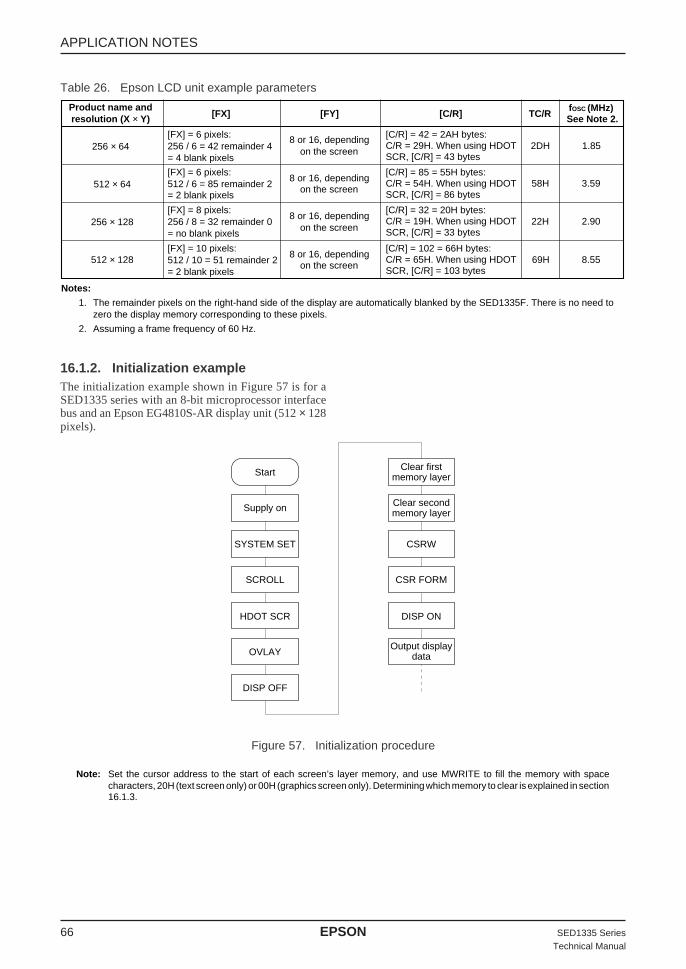
66 EPSON SED1335 SeriesTechnical Manual
Start Clear firstmemory layer
Supply on
SYSTEM SET
SCROLL
HDOT SCR
OVLAY
DISP OFF
Clear secondmemory layer
Output displaydata
CSRW
CSR FORM
DISP ON
Note: Set the cursor address to the start of each screen’s layer memory, and use MWRITE to fill the memory with spacecharacters, 20H (text screen only) or 00H (graphics screen only). Determining which memory to clear is explained in section16.1.3.
16.1.2. Initialization exampleThe initialization example shown in Figure 57 is for aSED1335 series with an 8-bit microprocessor interfacebus and an Epson EG4810S-AR display unit (512 × 128pixels).
Figure 57. Initialization procedure
APPLICATION NOTES
Table 26. Epson LCD unit example parameters
Product name andresolution (X × Y) [FX] [FY] [C/R] TC/R
fOSC (MHz)See Note 2.
8 or 16, depending256 × 64
512 × 64
256 × 128
512 × 128
on the screen
8 or 16, dependingon the screen
8 or 16, dependingon the screen
8 or 16, dependingon the screen
[FX] = 6 pixels:256 / 6 = 42 remainder 4= 4 blank pixels
[FX] = 6 pixels:512 / 6 = 85 remainder 2= 2 blank pixels
[FX] = 8 pixels:256 / 8 = 32 remainder 0= no blank pixels
[FX] = 10 pixels:512 / 10 = 51 remainder 2= 2 blank pixels
[C/R] = 42 = 2AH bytes:C/R = 29H. When using HDOTSCR, [C/R] = 43 bytes
[C/R] = 85 = 55H bytes:C/R = 54H. When using HDOTSCR, [C/R] = 86 bytes
[C/R] = 32 = 20H bytes:C/R = 19H. When using HDOTSCR, [C/R] = 33 bytes
[C/R] = 102 = 66H bytes:C/R = 65H. When using HDOTSCR, [C/R] = 103 bytes
Notes:
1. The remainder pixels on the right-hand side of the display are automatically blanked by the SED1335F. There is no need tozero the display memory corresponding to these pixels.
2. Assuming a frame frequency of 60 Hz.
1.85
3.59
2.90
2DH
58H
22H
69H 8.55
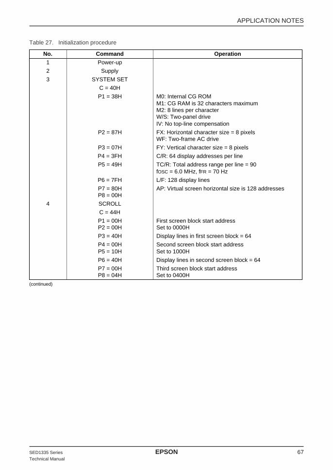
SED1335 Series EPSON 67Technical Manual
Table 27. Initialization procedure
No. Command Operation
1 Power-up
2 Supply
3 SYSTEM SET
C = 40H
P1 = 38H M0: Internal CG ROMM1: CG RAM is 32 characters maximumM2: 8 lines per characterW/S: Two-panel driveIV: No top-line compensation
P2 = 87H FX: Horizontal character size = 8 pixelsWF: Two-frame AC drive
P3 = 07H FY: Vertical character size = 8 pixels
P4 = 3FH C/R: 64 display addresses per line
P5 = 49H TC/R: Total address range per line = 90fOSC = 6.0 MHz, fFR = 70 Hz
P6 = 7FH L/F: 128 display lines
P7 = 80H AP: Virtual screen horizontal size is 128 addressesP8 = 00H
4 SCROLL
C = 44H
P1 = 00H First screen block start addressP2 = 00H Set to 0000H
P3 = 40H Display lines in first screen block = 64
P4 = 00H Second screen block start addressP5 = 10H Set to 1000H
P6 = 40H Display lines in second screen block = 64
P7 = 00H Third screen block start addressP8 = 04H Set to 0400H
(continued)
APPLICATION NOTES
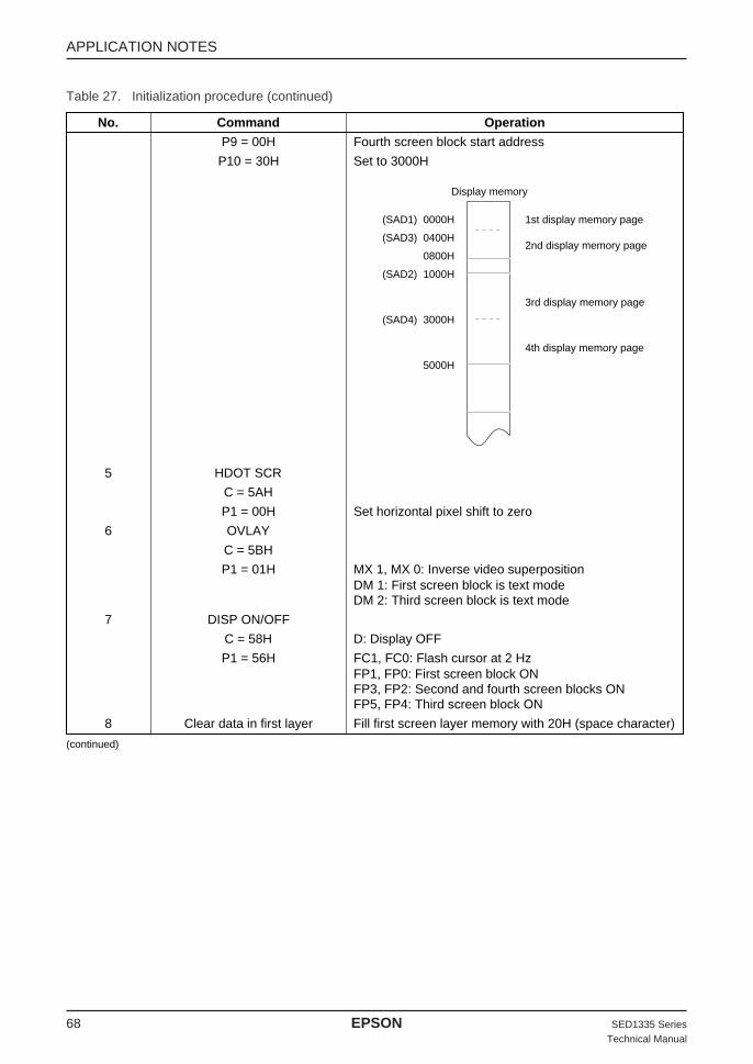
68 EPSON SED1335 SeriesTechnical Manual
Table 27. Initialization procedure (continued)
5 HDOT SCR
C = 5AH
P1 = 00H Set horizontal pixel shift to zero
6 OVLAY
C = 5BH
P1 = 01H MX 1, MX 0: Inverse video superpositionDM 1: First screen block is text modeDM 2: Third screen block is text mode
7 DISP ON/OFF
C = 58H D: Display OFF
P1 = 56H FC1, FC0: Flash cursor at 2 HzFP1, FP0: First screen block ONFP3, FP2: Second and fourth screen blocks ONFP5, FP4: Third screen block ON
8 Clear data in first layer Fill first screen layer memory with 20H (space character)
(continued)
No. Command Operation
P9 = 00H Fourth screen block start address
P10 = 30H Set to 3000H
Display memory
1st display memory page
2nd display memory page
3rd display memory page
4th display memory page
(SAD1) 0000H
(SAD3) 0400H
0800H
(SAD2) 1000H
(SAD4) 3000H
5000H
APPLICATION NOTES

SED1335 Series EPSON 69Technical Manual
Table 27. Initialization procedure (continued)
13 CSR DIR
C = 4CH Set cursor shift direction to right
(continued)
No. Command Operation
9 Clear data in second layer Fill second screen layer memory with 00H (blank data)
Display
1st layer
2nd layer
Blank code in every position
Character code in every position
10 CSRW
C = 46H
P1 = 00H Set cursor to start of first screen blockP2 = 00H
11 CSR FORM
C = 5DH
P1 = 04H CRX: Horizontal cursor size = 5 pixels
P2 = 86H CRY: Vertical cursor size = 7 pixelsCM: Block cursor
12 DISP ON/OFF
C = 59H Display ON
Display
APPLICATION NOTES
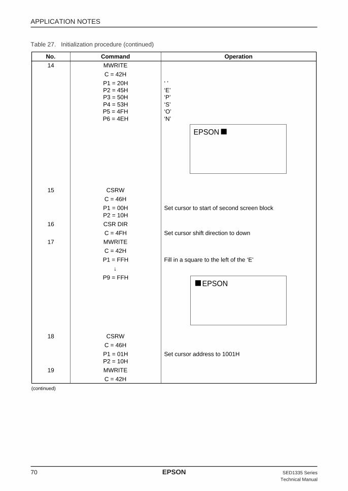
70 EPSON SED1335 SeriesTechnical Manual
Table 27. Initialization procedure (continued)
18 CSRW
C = 46H
P1 = 01H Set cursor address to 1001HP2 = 10H
19 MWRITE
C = 42H
(continued)
No. Command Operation
14 MWRITE
C = 42H
P1 = 20H ‘ ’P2 = 45H ‘E’P3 = 50H ‘P’P4 = 53H ‘S’P5 = 4FH ‘O’P6 = 4EH ‘N’
15 CSRW
C = 46H
P1 = 00H Set cursor to start of second screen blockP2 = 10H
16 CSR DIR
C = 4FH Set cursor shift direction to down
17 MWRITE
C = 42H
P1 = FFH Fill in a square to the left of the ‘E’
↓P9 = FFH
EPSON
EPSON
APPLICATION NOTES
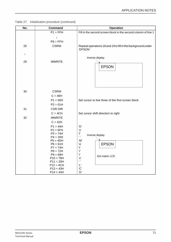
SED1335 Series EPSON 71Technical Manual
Table 27. Initialization procedure (continued)
30 CSRW
C = 46H
P1 = 00H Set cursor to line three of the first screen block
P2 = 01H
31 CSR DIR
C = 4CH Set cursor shift direction to right
32 MWRITE
C = 42H
P1 = 44H ‘D’P2 = 6FH ‘o’P3 = 74H ‘t’P4 = 20H ‘ ’P5 = 4DH ‘M’P6 = 61H ‘a’P7 = 74H ‘t’P8 = 72H ‘r’P9 = 69H ‘i’P10 = 78H ‘x’P11 = 20H ‘ ’P12 = 4CH ‘L’P13 = 43H ‘C’P14 = 44H ‘D’
No. Command Operation
P1 = FFH Fill in the second screen block in the second column of line 1
↓P9 = FFH
20 CSRW Repeat operations 18 and 19 to fill in the background under‘EPSON’
↓
29 MWRITE
EPSON
Inverse display
EPSON
Inverse display
Dot matrix LCD
APPLICATION NOTES

72 EPSON SED1335 SeriesTechnical Manual
16.1.3. Display mode setting example 1: combining text and graphics Conditions
• 320 × 200 pixels, single-panel drive (1/200 dutycycle)
• First layer: text display• Second layer: graphics display• 8 × 8-pixel character font• CG RAM not required
Display memory allocation• First layer (text): 320/8 = 40 characters per line,
200/8 = 25 lines. Required memory size = 40 × 25= 1000 bytes.
• Second layer (graphics): 320/8 = 40 characters perline, 200/1 = 200 lines. Required memory size = 40× 200 = 8000 bytes.
Figure 58. Character over graphics layers
Register setup procedureSYSTEM SET TC/R calculationC = 40HP1 = 30H fOSC = 6 MHzP2 = 87H fFR = 70 HzP3 = 07HP4 = 27H (1/6) × 9 × [TC/R] × 200 = 1/70P5 = 2FH [TC/R] = 48, so TC/R = 2FHP6 = C7HP7 = 28HP8 = 00H
SCROLLC = 44HP1 = 00HP2 = 00HP3 = C8HP4 = E8HP5 = 03HP6 = C8HP7 = XHP8 = XHP9 = XHP10 = XH
03E8H2nd graphics layer(8000 bytes)
2327H
0000H1st character layer(1000 bytes)
03E7H
APPLICATION NOTES

SED1335 Series EPSON 73Technical Manual
CSR FORMC = 5DHP1 = 04HP2 = 86H
HDOT SCRC = 5AHP1 = 00H
OVLAYC = 5BHP1 = 00H
DISP ON/OFFC = 59HP1 = 16H
X = Don’t care
16.1.4. Display mode setting example 2: combining graphics and graphics Conditions
• 320 × 200 pixels, single-panel drive (1/ 200 dutycycle)
• First layer: graphics display• Second layer: graphics display
Display memory allocation• First layer (graphics): 320/8 = 40 characters per
line, 200/1 = 200 lines. Required memory size = 40× 200 = 8000 bytes.
• Second layer (graphics): 320/8 = 40 characters perline, 200/1 = 200 lines. Required memory size =8000 bytes.
Figure 59. Two-layer graphics
1F40H2nd graphics layer(8000 bytes)
3E7FH
0000H1st graphics layer(8000 bytes)
1F3FH
APPLICATION NOTES
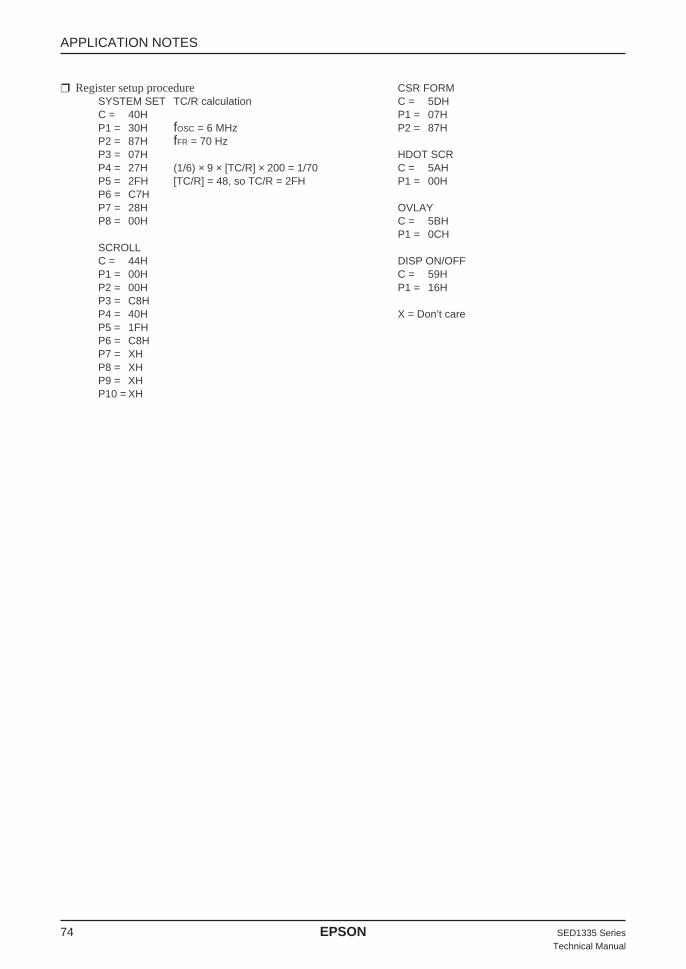
74 EPSON SED1335 SeriesTechnical Manual
Register setup procedureSYSTEM SET TC/R calculationC = 40HP1 = 30H fOSC = 6 MHzP2 = 87H fFR = 70 HzP3 = 07HP4 = 27H (1/6) × 9 × [TC/R] × 200 = 1/70P5 = 2FH [TC/R] = 48, so TC/R = 2FHP6 = C7HP7 = 28HP8 = 00H
SCROLLC = 44HP1 = 00HP2 = 00HP3 = C8HP4 = 40HP5 = 1FHP6 = C8HP7 = XHP8 = XHP9 = XHP10 = XH
CSR FORMC = 5DHP1 = 07HP2 = 87H
HDOT SCRC = 5AHP1 = 00H
OVLAYC = 5BHP1 = 0CH
DISP ON/OFFC = 59HP1 = 16H
X = Don’t care
APPLICATION NOTES

SED1335 Series EPSON 75Technical Manual
16.1.5. Display mode setting example 3: combining three graphics layers Conditions
• 320 × 200 pixels, single-panel drive (1/200 dutycycle)
• First layer: graphics display• Second layer: graphics display• Third layer: graphics display
Display memory allocation• All layers (graphics): 320/8 = 40 characters per
line, 200/1 = 200 lines. Required memory size = 40× 200 = 8000 bytes.
Figure 60. Three-layer graphics
Register setup procedureSYSTEM SET TC/R calculationC = 40HP1 = 30H fOSC = 6 MHzP2 = 87H fFR = 70 HzP3 = 07HP4 = 27H (1/6) × 9 × [TC/R] × 200 = 1/70P5 = 2FH [TC/R] = 48, so TC/R = 2FHP6 = C7HP7 = 28HP8 = 00H
5DBFH
1F40H2nd graphics layer(8000 bytes)
3E7FH
0000H1st graphics layer(8000 bytes)
1F3FH
3E80H3rd graphics layer(8000 bytes)
SCROLLC = 44HP1 = 00HP2 = 00HP3 = C8HP4 = 40HP5 = 1FHP6 = C8HP7 = 80HP8 = 3EHP9 = XHP10 = XH
APPLICATION NOTES
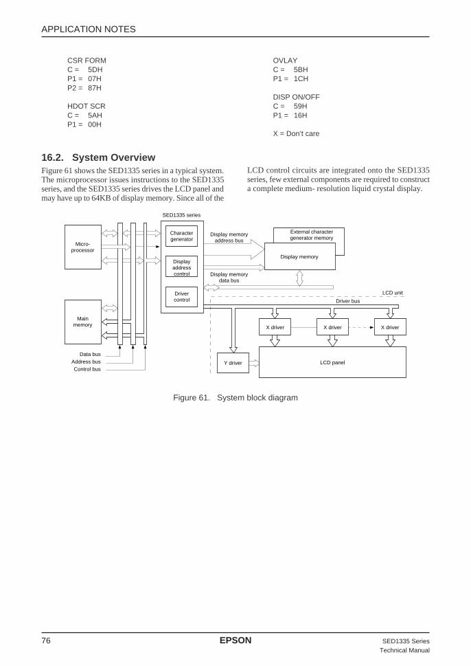
76 EPSON SED1335 SeriesTechnical Manual
CSR FORMC = 5DHP1 = 07HP2 = 87H
HDOT SCRC = 5AHP1 = 00H
OVLAYC = 5BHP1 = 1CH
DISP ON/OFFC = 59HP1 = 16H
X = Don’t care
16.2. System OverviewFigure 61 shows the SED1335 series in a typical system.The microprocessor issues instructions to the SED1335series, and the SED1335 series drives the LCD panel andmay have up to 64KB of display memory. Since all of the
LCD control circuits are integrated onto the SED1335series, few external components are required to constructa complete medium- resolution liquid crystal display.
Figure 61. System block diagram
External charactergenerator memory
Data busAddress busControl bus
Charactergenerator
Displayaddresscontrol
Drivercontrol
Y driver
Mainmemory
Micro-processor
Display memory
X driver X driver X driver
LCD panel
SED1335 series
Display memoryaddress bus
Display memorydata bus
LCD unit
Driver bus
APPLICATION NOTES

SED1335 Series EPSON 77Technical Manual
16.3. System Interconnection16.3.1. SED1335F
CS7CS6to
CS0
DILAT
INHFRYSCL
V1
V2
V3
V4
V5VREG
POFF
A0
A1to
A7
IORQ
D0to
D7
RDWR
RESET
Decoder
A0
CS
D0toD7
RDWRRESXD0toXD3
SED1335F
XG XD
VA13to
VA15VCEVRDVA0
toVA12
VD0to
VD7
XS
CL
XE
CL
LP WF
YD
ISY
DY
SC
L
A0 to A12
(RAM1)
D0 to D7
WE
CS1
CS2
OE
A0 to A12
(RAM2)
D0 to D7
WE
CS1
CS2
OE
A0 to A11
(CGROM)
D0 to D7
VA12
Y7Y6toY0
ABC
10MHz crystal
OE
CE
LCD UNIT
SED1600F
HC138
RESET
LCD
LP XS
CL
EC
LD
Oto D
3
E0FRE1
LP XS
CL
EC
LD
0to D
3
FREI
LP XS
CL
EC
LD
0to D
3
E0FREI
LP XS
CL
EC
LD
0to D
3E0
FREI
Powersupply
converter
Micro-processor
APPLICATION NOTES
Figure 62. System interconnection diagram

78 EPSON SED1335 SeriesTechnical Manual
The SED1335 series layered screens and flexible scroll-ing facilities support a range of display functions andreduces the load on the controlling microprocessor whendisplaying underlining, inverse display, text overlaid ongraphics or simple animation.These facilities are supported by the SED1335 seriesability to divide display memory into up to four differentareas. Character code table
• Contains character codes for text display• Each character requires 8 bits• Table mapping can be changed by using the scroll
start function Graphics data table
• Contains graphics bitmaps• Word length is 8 bits• Table mapping can be changed
CG RAM table• Character generator memory can be modified by
the external microprocessor• Character sizes up to 8 × 16-pixels (16 bytes per
character)• Maximum of 64 characters• Table mapping can be changed
CG ROM table• Used when the internal character generator is not
adequate• Can be used in conjunction with the internal char-
acter generator and external character generatorRAM
• Character sizes up to 8 × 16-pixels (16 bytes percharacter)
• Maximum of 256 characters• Fixed mapping at F000H to FFFFH
APPLICATION NOTES

SED1335 Series EPSON 79Technical Manual
16.4. Smooth Horizontal ScrollingFigure 63 illustrates smooth display scrolling to the left.When scrolling left, the screen is effectively moving tothe right, over the larger virtual screen.Instead of changing the display start address SAD andshifting the display by eight pixels, smooth scrolling isachieved by repeatedly changing the pixel-shift param-eter of the HDOT SCR command. When the display hasbeen scrolled seven pixels, the HDOT SCR pixel-shiftparameter is reset to zero and SAD incremented by one.Repeating this operation at a suitable rate gives theappearance of smooth scrolling.
To scroll the display to the right, the reverse procedure isfollowed.When the edge of the virtual screen is reached, themicroprocessor must take appropriate steps so that thedisplay is not corrupted. The scroll must be stopped or thedisplay modified.Note that the HDOT SCR command cannot be used toscroll individual layers.
Figure 63. HDOT SCR example
Display
APAP
P1 = 00H
P1 = 01H
P1 = 02H
P1 = 03H
P1 = 07H
P1 = 00H
HDOT SCRparameter
SAD SAD + 1 SAD + 2
SAD = SAD + 1
SAD = SAD
Not visible Visible
C/R
Virtual screen
Magnified
Note: The response time of LCD panels changes considerably at low temperatures. Smooth scrolling under these conditions maymake the display difficult to read.
APPLICATION NOTES
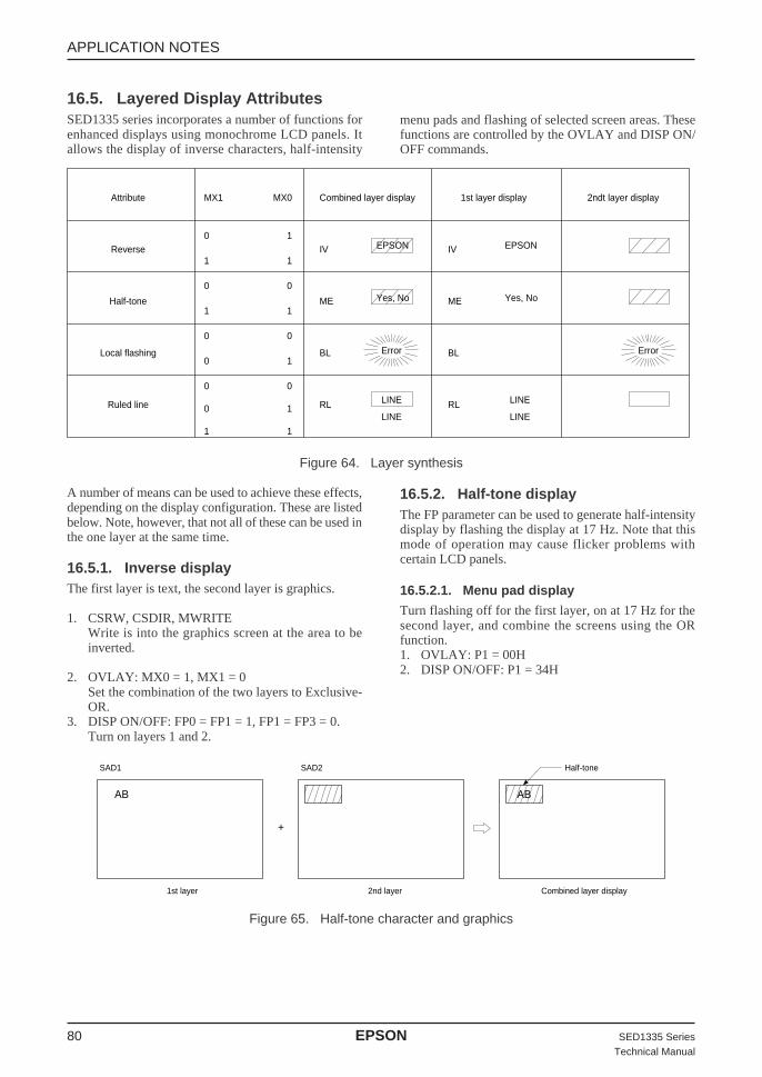
80 EPSON SED1335 SeriesTechnical Manual
16.5. Layered Display AttributesSED1335 series incorporates a number of functions forenhanced displays using monochrome LCD panels. Itallows the display of inverse characters, half-intensity
menu pads and flashing of selected screen areas. Thesefunctions are controlled by the OVLAY and DISP ON/OFF commands.
Figure 64. Layer synthesis
A number of means can be used to achieve these effects,depending on the display configuration. These are listedbelow. Note, however, that not all of these can be used inthe one layer at the same time.
16.5.1. Inverse displayThe first layer is text, the second layer is graphics.
1. CSRW, CSDIR, MWRITEWrite is into the graphics screen at the area to beinverted.
2. OVLAY: MX0 = 1, MX1 = 0Set the combination of the two layers to Exclusive-OR.
3. DISP ON/OFF: FP0 = FP1 = 1, FP1 = FP3 = 0.Turn on layers 1 and 2.
Error
Attribute
Reverse
Half-tone
Local flashing
Ruled line
MX1
0
1
0
1
0
0
0
0
1
MX0
1
1
0
1
0
1
0
1
1
Combined layer display
IV
ME
BL
RL LINE
LINE
Yes, No
EPSON
Error
1st layer display
IV
ME
BL
RL LINE
LINE
Yes, No
EPSON
2ndt layer display
16.5.2. Half-tone displayThe FP parameter can be used to generate half-intensitydisplay by flashing the display at 17 Hz. Note that thismode of operation may cause flicker problems withcertain LCD panels.
16.5.2.1. Menu pad display
Turn flashing off for the first layer, on at 17 Hz for thesecond layer, and combine the screens using the ORfunction.1. OVLAY: P1 = 00H2. DISP ON/OFF: P1 = 34H
Figure 65. Half-tone character and graphics
AB
SAD1
1st layer
SAD2
2nd layer
AB
Combined layer display
+
Half-tone
APPLICATION NOTES

SED1335 Series EPSON 81Technical Manual
16.5.2.2. Graph display
To present two overlaid graphs on the screen, configurethe display as for the menu bar display and put one graphon each screen layer. The difference in contrast betweenthe half- and full-intensity displays will make it easy to
distinguish between the two graphs and help create anattractive display.1. OVLAY: P1 = 00H2. DISP ON/OFF: P1 = 34H
16.5.3. Flashing areas16.5.3.1 Small area
To flash selected characters, the MPU can alternatelywrite the characters as character codes and blank charac-ters at intervals of 0.5 to 1.0 seconds.
16.5.3.2. Large area
Divide both layer 1 and layer 2 into two screen blockseach, layer 2 being divided into the area to be flashed andthe remainder of the screen. Flash the layer 2 screenblock at 2 Hz for the area to be flashed and combine thelayers using the OR function.
16.6. 16 × 16-dot Graphic Display16.6.1. Command usageThis example shows how to display 16 × 16-pixelcharacters. The command sequence is as follows:
CSRW Set the cursor address.CSRDIR Set the cursor auto-increment direction.MWRITE Write to the display memory.
16.6.2. Kanji character displayThe program for writing large characters operates asfollows:1. The microprocessor reads the character data from its
ROM.2. The microprocessor sets the display address and
writes to the VRAM. The flowchart is shown inFigure 69.
Figure 66. Localized flashing
ABC
XYZ
ABC
XYZ
APPLICATION NOTES

82 EPSON SED1335 SeriesTechnical Manual
Figure 67. Graphics address indexing
(1)(3)(5)(7)(9)(11)(13)(15)(17)(19)(21)(23)(25)(27)(29)(31)
(2)(4)(6)(8)(10)(12)(14)(16)(18)(20)(22)(24)(26)(28)(30)(32)
O8 O7 O6 O5 O4 O3 O2 O1 O8 O7 O6 O5 O4 O3 O2 O1
(6)(4)(2)
(19)(17)(15)(13)(11)(9)(7)(5)(3)(1)
0H1H2H3H4H5H6H7H8H9HAHBHCHDHEHFH
Data held in the microprocessor memory
Scan address A1 to A41st column 2nd column
(n) shows the CG ROM datareadout order
(Kanji ROM pattern)
CG ROM output
A0 = 0 A0 = 1
(4)(2)
(3)(1)
Data written into the SED1330 display memory
2nd columnmemory area
1st columnmemory area
APPLICATION NOTES

SED1335 Series EPSON 83Technical Manual
Figure 68. Graphics bit map
Figure 69. 16 × 16-dot display flowchart
Using an external character generator ROM, and 8 × 16-pixel font can be used, allowing a 16 × 16-pixel characterto be displayed in two segments. The external CG ROMEPROM data format is described in Section 9.1. This willallow the display of up to 128, 16 × 16-pixel characters.If CG RAM is also used, 96 fixed characters and 32 bank-switchable characters can also be supported.
(1)(3)(5)(7)(9)
(11)(13)(15)(17)(19)(21)(23)(25)(27)(29)(31)
(2)(4)(6)(8)(10)(12)(14)(16)(18)(20)(22)(24)(26)(28)(30)(32)
Direction of cursor movement
240 dots
320 dots
Start
Enable cursor downwards movement
Set column 1 cursor address
Write data
Set column 2 cursor address
Write data
End
APPLICATION NOTES

84 EPSON SED1335 SeriesTechnical Manual
17. INTERNAL CHARACTER GENERATOR FONT
Figure 70. On-chip character set
NoteThe shaded positions indecate characters that have the whole 6 × 8 bitmap blackened.
0 1 2 3 4 5 6 7 8 9 A B C D E F
2
3
4
5
6
7
A
B
C
D
1
Character code bits 0 to 3
Cha
ract
er c
ode
bits
4 to
7
INTERNAL CHARACTER GENERATOR FONT

SED1335 Series EPSON 85Technical Manual
18. GLOSSARY OF TERMSA AddressAP Address pitch parameterC Character display modeCD Cursor direction of movement parameterCG Character generatorCGRAM ADR Character generator memory addressCM Cursor display shape parameterC/R Characters per row parameterCRX Horizontal cursor size parameterCRY Vertical cursor size parameterCSR DIR Cursor direction of movement instructionCSR FORM Cursor size, position and type instructionCSRR Read cursor address register instructionCSRW Write cursor address register instructionDM Display mode parameterFC Flashing cursor parameterfFR Frame frequencyfOSC Oscillator frequencyFP Screen flashing parameterFX Horizontal character size parameterFY Vertical character size parameterG Graphics display modeGLC Graphic line control unitHDOT SCR Horizontal scrolling by pixels instructionIV Screen origin compensation for inverse displayL/F Lines per frame instructionMREAD Display memory read instructionMWRITE Display memory write instructionMX Screen composition modeOV Graphics layer select parameterOVLAY Screen layer mode instructionP ParameterR RowRAM Random access memoryROM Read only memorySAD Display scrolling start address parameterSL Display scrolling length parameterTC/R Length, including horizontal blanking, of one screen lineVRAM Display memoryWF Display drive waveform parameterW/S Windows per screen parameter
GLOSSARY OF TERMS

86 EPSON SED1335 SeriesTechnical Manual
Request for Information on SED1335 SeriesDated:__________, 19____
Company: Name of the inquiring person:
The phenomenon occurred on: Desired date of receiving the reply: ______________
Device name: SED1335F0A / SED1335F0B (Lot No. )Number of units of the device causing the phenomenon: __units Applications:(Scope of occurrence: ___ / ___)
Your address:Documents in your current possession:
Your phone number: - - FAX: - -
Image plane size: ____ dots × ____ dots (single-plane drive/2-plane drive)
Using LCD module (manufacturer): Frame frequency: Hz.
Display mode (circle either one)
(1) First layer: Characters Two-part plane, Second layer: Graphics Single plane(2) First layer: Characters Single plane, Second layer: Graphics Single plane < (1)' >(3) First layer: Characters Two-part plane, Second layer: Graphics Two-part plane(4) First layer: Graphics Two-part plane, Second layer: Graphics Single plane(5) First layer: Graphics Single plane, Second layer: Graphics Single plane < (4)' >(6) First layer: Graphics Single plane, Second layer: Graphics Single plane, Third layer: Graphics Single plane(7) First layer: Graphics Two-part plane, Second layer: Graphics Two-part plane
Initialization parameter: Give in decimals or duodecimals.
System setting Scroll HDOT SCR CSRFORMP1(IV, W/S, M2, M1, M0) = P1(SADIL) = P1 = P1 =P2(W/F, FX) = P2(SADIH) = OVLAY P2 =P3(FY) = P3(SL1) = P1 =P4(C/R) = P4(SAD2L) = DISP ON/OFFP5(TC/R) = P5(SAD2H) = P1 =P6(L/F) = P6(SL2) = CSRWP7(APL) = P7(SAD3L) = P1 =P8(APH) = P8(SAD3H) = P2 =
P9(SAD4L) = CSR DIRP10(SAD4H) = C =
Oscillation frequency: MHz. (internal/external)
CPU: CPU clock: MHz.
Frame memory capacity: Kb. (using memory IC: , access time: nsec.)
Descriptions of your inquiry (Give details such as what type of display is being sought for and which phenomenon is occurring.)
Attached documents (circuit diagram, timing chart, program list, or others)
GLOSSARY OF TERMS
- - - - - - - - - - - - - - - - - - - - - - - - - - - - - - - - - - - - - - - - - - - - - - - - - - - - - - - - - - - - - - - - -
- - - - - - - - - - - - - - - - - - - - - - - - - - - - - - - - - - - - - - - - - - - - - - - - - - - - - - - - - - - - - - - - -

AMERICAEPSON ELECTRONICS AMERICA, INC.HEADQUARTERS1960 E. Grand AveEl Segundo, CA 90245, U.S.A.Phone : +1-310-955-5300 Fax : +1-310-955-5400
SALES OFFICESWest150 River Oaks ParkwaySan Jose, CA 95134, U.S.A.Phone : +1-408-922-0200 Fax : +1-408-922-0238
Central1450 East American Lane Suite 1550Schaumburg, IL 60173, U.S.A.Phone : +1-847-517-7667 Fax : +1-847-517-7601
101 Virginia Street, Suite 290Crystal Lake, IL 60014, U.S.A.Phone : +1-815-455-7630 Fax : +1-815-455-7633
Northeast301 Edgewater Place, Suite 120Wakefield, MA 01880, U.S.A.Phone : +1-781-246-3600 Fax : +1-781-246-5443
Southeast4300 Six Forks Road, Suite 430Raleigh, NC 27609, U.S.A.Phone : +1-919-781-7667 Fax : +1-919-781-6778
1700 Spinnaker DriveAlptaretta, GA 30005, U.S.A.Phone : +1-770-754-4872 Fax : +1-770-753-0601
EUROPEEPSON EUROPE ELECTRONICS GmbHHEADQUARTERSRiesstrasse 1580992 Muenchen, GERMANYPhone : +49- (0) 89-14005-0 Fax : +49- (0) 89-14005-110
- GERMANY -SALES OFFICEBreidenbachstrasse 46D-51373 Leverkusen, GERMANYPhone : +49- (0) 214-83070-0 Fax : +49- (0) 214-83070-10
- UNITED KINGDOM -UK BRANCH OFFICEG6 Doncastle House, Doncastle RoadBracknell, Berkshire RG12 8PE, ENGLANDPhone : +44- (0) 1344-381700 Fax : +44- (0) 1344-381701
- FRANCE -FRENCH BRANCH OFFICE1 Avenue de l’ Atlantique, LP 915 Les ConquerantsZ.A. de Courtaboeuf 2, F-91976 Les Ulis Cedex, FRANCEPhone : +33- (0) 1-64862350 Fax : +33- (0) 1-64862355
ASIA- HONG KONG, CHINA -EPSON HONG KONG LTD.20/F., Harbour Centre, 25 Harbour RoadWanchai, HONG KONGPhone : +852-2585-4600 Fax : +852-2827-4346Telex : 65542 EPSCO HX
- CHINA -SHANGHAI EPSON ELECTRONICS CO., LTD.4F, Bldg., 27, No. 69, Gui Jing RoadCaohejing, Shanghai, CHINAPhone : 21-6485-5552 Fax : 21-6485-0775
- TAIWAN, R.O.C. -EPSON TAIWAN TECHNOLOGY & TRADING LTD.10F, No. 287,Nanking East Road, Sec. 3Taipei, TAIWAN, R.O.C.Phone : 02-2717-7360 Fax : 02-2712-9164Telex : 24444 EPSONTB
HSINCHU OFFICE13F-3, No.295, Kuang-Fu Road, Sec. 2HsinChu 300, TAIWAN, R.O.C.Phone : 03-573-9900 Fax : 03-573-9169
- SINGAPORE -EPSON SINGAPORE PTE., LTD.No. 1 Temasek Avenue, #36-00Millenia Tower, SINGAPORE 039192Phone : +65-337-7911 Fax : +65-334-2716
- KOREA -SEIKO EPSON CORPORATIONKOREA OFFICE50F, KLI 63 Bldg., 60 Yoido-DongYoungdeungpo-Ku, Seoul, 150-010, KOREAPhone : 02-784-6027 Fax : 02-767-3677
- JAPAN -SEIKO EPSON CORPORATIONELECTRONIC DEVICES MARKETING DIVISION
Electronic Device Marketing DepartmentIC Marketing & Engineering Group421-8, Hino, Hino-shi, Tokyo 191-8501, JAPANPhone: +81-(0)42-587-5816 Fax: +81-(0)42-587-5624
ED International Marketing Department I (Europe & U.S.A.)421-8, Hino, Hino-shi, Tokyo 191-8501, JAPANPhone: +81-(0)42-587-5812 Fax: +81-(0)42-587-5564
ED International Marketing Department II (Asia)421-8, Hino, Hino-shi, Tokyo 191-8501, JAPANPhone: +81-(0)42-587-5814 Fax: +81-(0)42-587-5110
International Sales Operations

In pursuit of “Saving” Technology, Epson electronic devices.
Our lineup of semiconductors, liquid crystal displays and quartz devices
assists in creating the products of our customers’ dreams.
Epson IS energy savings.
SED 1335 SeriesLCD Controller ICs
First issue March, 1999
Printed in Japan H A
Electronic Devices Information on the EPSON WWW Server
ELECTRONIC DEVICES MARKETING DIVISION
With collaboration of https://www.displayfuture.com