mipi csi-2 transmit subsystem v1 - xilinx · 2019-10-10 · mipi csi-2 tx subsystem v1.0 6 pg260...
TRANSCRIPT

MIPI CSI-2 Transmit Subsystem v1.0
Product Guide
Vivado Design Suite
PG260 June 7, 2017
MIPI CSI-2 TX Subsystem v1.0 www.xilinx.com 2PG260 June 7, 2017
Table of ContentsIP Facts
Chapter 1: OverviewSub-Core Details. . . . . . . . . . . . . . . . . . . . . . . . . . . . . . . . . . . . . . . . . . . . . . . . . . . . . . . . . . . . . . . . . . . 6Applications . . . . . . . . . . . . . . . . . . . . . . . . . . . . . . . . . . . . . . . . . . . . . . . . . . . . . . . . . . . . . . . . . . . . . . 7Unsupported Features. . . . . . . . . . . . . . . . . . . . . . . . . . . . . . . . . . . . . . . . . . . . . . . . . . . . . . . . . . . . . . 7Licensing and Ordering Information . . . . . . . . . . . . . . . . . . . . . . . . . . . . . . . . . . . . . . . . . . . . . . . . . . . 8
Chapter 2: Product SpecificationStandards . . . . . . . . . . . . . . . . . . . . . . . . . . . . . . . . . . . . . . . . . . . . . . . . . . . . . . . . . . . . . . . . . . . . . . . . 9Resource Utilization. . . . . . . . . . . . . . . . . . . . . . . . . . . . . . . . . . . . . . . . . . . . . . . . . . . . . . . . . . . . . . . . 9Port Descriptions . . . . . . . . . . . . . . . . . . . . . . . . . . . . . . . . . . . . . . . . . . . . . . . . . . . . . . . . . . . . . . . . . . 9Pixel Encoding . . . . . . . . . . . . . . . . . . . . . . . . . . . . . . . . . . . . . . . . . . . . . . . . . . . . . . . . . . . . . . . . . . . 13Register Space . . . . . . . . . . . . . . . . . . . . . . . . . . . . . . . . . . . . . . . . . . . . . . . . . . . . . . . . . . . . . . . . . . . 15
Chapter 3: Designing with the SubsystemGeneral Design Guidelines . . . . . . . . . . . . . . . . . . . . . . . . . . . . . . . . . . . . . . . . . . . . . . . . . . . . . . . . . 22Shared Logic . . . . . . . . . . . . . . . . . . . . . . . . . . . . . . . . . . . . . . . . . . . . . . . . . . . . . . . . . . . . . . . . . . . . . 22I/O Planning . . . . . . . . . . . . . . . . . . . . . . . . . . . . . . . . . . . . . . . . . . . . . . . . . . . . . . . . . . . . . . . . . . . . . 24Clocking. . . . . . . . . . . . . . . . . . . . . . . . . . . . . . . . . . . . . . . . . . . . . . . . . . . . . . . . . . . . . . . . . . . . . . . . . 26Resets . . . . . . . . . . . . . . . . . . . . . . . . . . . . . . . . . . . . . . . . . . . . . . . . . . . . . . . . . . . . . . . . . . . . . . . . . . 27Protocol Description . . . . . . . . . . . . . . . . . . . . . . . . . . . . . . . . . . . . . . . . . . . . . . . . . . . . . . . . . . . . . . 28
Chapter 4: Design Flow StepsCustomizing and Generating the Subsystem . . . . . . . . . . . . . . . . . . . . . . . . . . . . . . . . . . . . . . . . . . . 30Constraining the Subsystem . . . . . . . . . . . . . . . . . . . . . . . . . . . . . . . . . . . . . . . . . . . . . . . . . . . . . . . . 35Simulation . . . . . . . . . . . . . . . . . . . . . . . . . . . . . . . . . . . . . . . . . . . . . . . . . . . . . . . . . . . . . . . . . . . . . . 37Synthesis and Implementation . . . . . . . . . . . . . . . . . . . . . . . . . . . . . . . . . . . . . . . . . . . . . . . . . . . . . . 37
Appendix A: Verification, Compliance, and InteroperabilityHardware Validation . . . . . . . . . . . . . . . . . . . . . . . . . . . . . . . . . . . . . . . . . . . . . . . . . . . . . . . . . . . . . . 38
Appendix B: DebuggingFinding Help on Xilinx.com . . . . . . . . . . . . . . . . . . . . . . . . . . . . . . . . . . . . . . . . . . . . . . . . . . . . . . . . . 39
Send Feedback
MIPI CSI-2 TX Subsystem v1.0 www.xilinx.com 3PG260 June 7, 2017
Debug Tools . . . . . . . . . . . . . . . . . . . . . . . . . . . . . . . . . . . . . . . . . . . . . . . . . . . . . . . . . . . . . . . . . . . . . 40Hardware Debug . . . . . . . . . . . . . . . . . . . . . . . . . . . . . . . . . . . . . . . . . . . . . . . . . . . . . . . . . . . . . . . . . 41Interface Debug . . . . . . . . . . . . . . . . . . . . . . . . . . . . . . . . . . . . . . . . . . . . . . . . . . . . . . . . . . . . . . . . . . 41
Appendix C: Additional Resources and Legal NoticesXilinx Resources . . . . . . . . . . . . . . . . . . . . . . . . . . . . . . . . . . . . . . . . . . . . . . . . . . . . . . . . . . . . . . . . . . 44References . . . . . . . . . . . . . . . . . . . . . . . . . . . . . . . . . . . . . . . . . . . . . . . . . . . . . . . . . . . . . . . . . . . . . . 44Revision History . . . . . . . . . . . . . . . . . . . . . . . . . . . . . . . . . . . . . . . . . . . . . . . . . . . . . . . . . . . . . . . . . . 45Please Read: Important Legal Notices . . . . . . . . . . . . . . . . . . . . . . . . . . . . . . . . . . . . . . . . . . . . . . . . 45
Send Feedback

MIPI CSI-2 TX Subsystem v1.0 www.xilinx.com 4PG260 June 7, 2017 Product Specification
IntroductionThe Mobile Industry Processor Interface (MIPI) Camera Serial Interface (CSI-2) TX subsystem implements a CSI-2 transmit interface according to the MIPI CSI-2 standard, v1.1 [Ref 1]. The CSI-2 TX subsystem packs the incoming pixel data to CSI-2 packets with the required pixel to byte conversion, header and footer insertion. Also generates the required frame and line marker packets. These packets are then sent over DPHY interface for transmission.
Features• Support for 1 to 4 D-PHY lanes
• Maximum data rate of 1.5 Gb/s
• Multiple data type support (RAW, RGB, YUV, User defined)
• Support for single, dual, quad pixel modes
• Support for 1 to 4 virtual channels
• Low power state (LPS) insertion between the packets
• Ultra low power (ULP) mode generation using register access
• Interrupt generation to indicate subsystem status information
• AXI4-Lite interface for register access to configure different subsystem options
• Configurable Line Start/Line End packet generation
• Configurable selection of D-PHY register interface
IP Facts
IP Facts Table
Subsystem Specifics
Supported Device Family(1)
UltraScale+™ Families,Zynq® UltraScale+ MPSoC,
Zynq®-7000 All Programmable SoC,Virtex®-7, Kintex®-7, Artix®-7
Supported User Interfaces AXI4-Lite, AXI4-Stream, Native Video
Resources Performance and Resource Utilization webpage
Provided with SubsystemDesign Files Encrypted RTL
Example Design Not Provided
Test Bench Not Provided
Constraints File XDC
Simulation Model Not Provided
Supported S/W Driver(2) Standalone
Tested Design Flows(3)
Design Entry Vivado® Design Suite
Simulation For supported simulators, see theXilinx Design Tools: Release Notes Guide.
Synthesis Vivado Synthesis
SupportProvided by Xilinx at the Xilinx Support web page
Notes: 1. For a complete list of supported devices, see the Vivado IP
catalog.2. Standalone driver details can be found in the SDK directory
(<install_directory>/SDK/<release>/data/embeddedsw/doc/xilinx_drivers.htm). Linux OS and driver support information is available from the Xilinx Wiki page.
3. For the supported versions of the tools, see theXilinx Design Tools: Release Notes Guide.
Send Feedback

MIPI CSI-2 TX Subsystem v1.0 www.xilinx.com 5PG260 June 7, 2017
Chapter 1
OverviewThe MIPI CSI-2 TX subsystem allows you to quickly create systems based on the MIPI protocol. It interfaces between image sensors and an image sensor pipe. An internal high speed physical layer design, D-PHY, is provided that allows direct connection to MIPI based receivers. The top level customization parameters select the required hardware blocks needed to build the subsystem. Figure 1-1 shows the subsystem architecture.
The subsystem consists of the following sub-cores:
• MIPI D-PHY
• MIPI CSI-2 TX Controller
• AXI Crossbar
X-Ref Target - Figure 1-1
Figure 1-1: Subsystem Architecture
MIPI CSI2 Tx
Controller
MIPI DPHY/ Serial Interface
AXI Cross Bar
AXI4-LiteInterface
PPI
dphy_clk_200M
s_axis_aclk
s_axis_aresetn
Native Video / AXIS Interface
Send Feedback

MIPI CSI-2 TX Subsystem v1.0 www.xilinx.com 6PG260 June 7, 2017
Chapter 1: Overview
Sub-Core Details
MIPI D-PHY The MIPI D-PHY IP core implements a D-PHY TX interface and provides PHY protocol layer support compatible with the CSI-2 TX interface. MIPI I/O bank support & I/O Planner are present only for UltraScale+ devices. For more details, refer MIPI D-PHY LogiCORE IP Product Guide (PG202) [Ref 3].
MIPI CSI-2 TX Controller CSI provides the mobile industry a standard, robust, scalable, low-power, high-speed, cost-effective interface that supports a wide range of imaging solutions for mobile devices.
MIPI CSI-2 TX Controller receives stream of image data via Native video or AXI4-Stream input interface. The controller adds the synchronization packets and performs the pixel-to-byte conversions for the pixel data. Packed byte data is sent over the D-PHY interface for transmission. AXI4-Lite interface is used to access core registers. The MIPI CSI2-TX Controller supports ECC and CRC generation for header and payload respectively.
Features of this core include:
• Multi-lane interoperability that allows more bandwidth than that provided by one lane. Those trying to avoid high clock rates, can expand the data path to multiple lanes and obtain approximately linear increases in peak bus bandwidth
• Short and long packets with all word count values supported and can be used for low level protocol communication
X-Ref Target - Figure 1-2
Figure 1-2: MIPI CSI-2 TX Controller Core
image_iface PacketizerLane
Distribution Block
Native Video / AXIS Interface
PPI
Register Module
Synchronization Module
AXI4 Lite Interface
ECC
CRC
line buffer
Interrupt
Send Feedback

MIPI CSI-2 TX Subsystem v1.0 www.xilinx.com 7PG260 June 7, 2017
Chapter 1: Overview
• Error Correction Code (ECC) for error generation in Long and Short packet header. To detect possible errors in transmission, a checksum is calculated over each data packet. The checksum is realized as 16-bit CRC. The generator polynomial is x16+x12+x5+x0
• Supports embedded non-image data transmission using the same input Native video or AXI4S interface.
• Supports active lane configuration, programmable native video interface or AXI4 streaming interface, and programmable CRC generation.
AXI CrossbarThe AXI Crossbar core is used in the subsystem to route AXI4-Lite requests to corresponding sub-cores based on the address. See the AXI Interconnect LogiCORE IP Product Guide [Ref 4] for details.
ApplicationsThe Xilinx MIPI CSI-2 TX controller implements camera sensor transmit interface over MIPI D-PHY interface. It can be used to bridge between non-MIPI camera sensors to MIPI based image sensor processors or to map video data captured over other interfaces such as HDMI and DisplayPort™ to a MIPI CSI interface. MIPI is a group of protocols defined by the mobile industry group to standardize all interfaces within mobile platforms such as mobile phones and tablets. However the large volumes and the economies of scale of the mobile industry is forcing other applications to also adopt these standards. As such MIPI-based camera sensors and Image sensor processors are being increasingly used in applications such as driver assistance technologies in automotive applications, video security surveillance cameras, video conferencing and emerging applications such as virtual and augmented reality.
Unsupported Features• Secondary data types excluding RAW12,RAW14 are not supported.
Send Feedback

MIPI CSI-2 TX Subsystem v1.0 www.xilinx.com 8PG260 June 7, 2017
Chapter 1: Overview
Licensing and Ordering Information
License CheckersIf the IP requires a license key, the key must be verified. The Vivado® design tools have several license checkpoints for gating licensed IP through the flow. If the license check succeeds, the IP can continue generation. Otherwise, generation halts with error. License checkpoints are enforced by the following tools:
• Vivado synthesis
• Vivado implementation
• write_bitstream (Tcl command)
IMPORTANT: IP license level is ignored at checkpoints. The test confirms a valid license exists. It does not check IP license level.
License TypeThis Xilinx module is provided under the terms of the Xilinx Core License Agreement. The module is shipped as part of the Vivado® Design Suite. For full access to all core functionalities in simulation and in hardware, you must purchase a license for the core. Contact your local Xilinx sales representative for information about pricing and availability.
For more information, visit the MIPI CSI-2 TX Subsystem product web page.
Information about other Xilinx LogiCORE IP modules is available at the Xilinx Intellectual Property page. For information on pricing and availability of other Xilinx LogiCORE IP modules and tools, contact your local Xilinx sales representative.
Send Feedback

MIPI CSI-2 TX Subsystem v1.0 www.xilinx.com 9PG260 June 7, 2017
Chapter 2
Product Specification
Standards• MIPI Alliance Standard for Camera Serial Interface CSI-2 v1.1 [Ref 1]
• MIPI Alliance Physical Layer Specifications, D-PHY Specification v1.1 [Ref 6]
• Processor Interface, AXI4-Lite: see the Vivado Design Suite: AXI Reference Guide (UG1037) [Ref 7]
• Input Pixel Interface: see the AXI4-Stream Video IP and System Design Guide (UG934) [Ref 2]
Resource UtilizationFor full details about performance and resource utilization, visit the Performance and Resource Utilization web page.
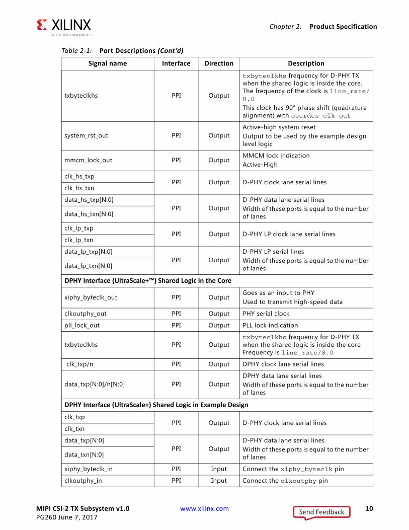
Port DescriptionsThe MIPI CSI-2 TX Subsystem I/O signals are described in Table 2-1.
Table 2-1: Port Descriptions
Signal name Interface Direction Description
DPHY Interface (7 Series family) Shared Logic in the Core
txclkesc_out PPI Output Use to connect the txclkesc pin.
oserdes_clk_out PPI Output Use to connect the OSERDES clock pin. Frequency of the clock is line_rate/2
Send Feedback
MIPI CSI-2 TX Subsystem v1.0 www.xilinx.com 10PG260 June 7, 2017
Chapter 2: Product Specification
txbyteclkhs PPI Output
txbyteclkhs frequency for D-PHY TX when the shared logic is inside the core. The frequency of the clock is line_rate/8.0
This clock has 90° phase shift (quadrature alignment) with oserdes_clk_out
system_rst_out PPI OutputActive-high system resetOutput to be used by the example design level logic
mmcm_lock_out PPI OutputMMCM lock indicationActive-High
clk_hs_txpPPI Output D-PHY clock lane serial lines
clk_hs_txn
data_hs_txp[N:0]PPI Output
D-PHY data lane serial linesWidth of these ports is equal to the number of lanesdata_hs_txn[N:0]
clk_lp_txpPPI Output D-PHY LP clock lane serial lines
clk_lp_txn
data_lp_txp[N:0]PPI Output
D-PHY LP serial linesWidth of these ports is equal to the number of lanesdata_lp_txn[N:0]
DPHY Interface (UltraScale+™) Shared Logic in the Core
xiphy_byteclk_out PPI OutputGoes as an input to PHYUsed to transmit high-speed data
clkoutphy_out PPI Output PHY serial clock
pll_lock_out PPI Output PLL lock indication
txbyteclkhs PPI Outputtxbyteclkhs frequency for D-PHY TX when the shared logic is inside the core Frequency is line_rate/8.0
clk_txp/n PPI Output DPHY clock lane serial lines
data_txp[N:0]/n[N:0] PPI OutputDPHY data lane serial linesWidth of these ports is equal to the number of lanes
DPHY Interface (UltraScale+) Shared Logic in Example Design
clk_txpPPI Output D-PHY clock lane serial lines
clk_txn
data_txp[N:0]PPI Output
D-PHY data lane serial linesWidth of these ports is equal to the number of lanesdata_txn[N:0]
xiphy_byteclk_in PPI Input Connect the xiphy_byteclk pin
clkoutphy_in PPI Input Connect the clkoutphy pin
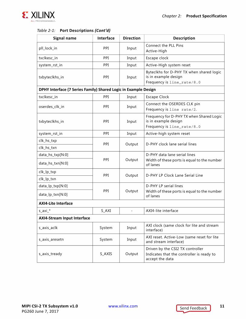
Table 2-1: Port Descriptions (Cont’d)
Signal name Interface Direction Description
Send Feedback
MIPI CSI-2 TX Subsystem v1.0 www.xilinx.com 11PG260 June 7, 2017
Chapter 2: Product Specification
pll_lock_in PPI InputConnect the PLL PinsActive-High
txclkesc_in PPI Input Escape clock
system_rst_in PPI Input Active-High system reset
txbyteclkhs_in PPI InputByteclkhs for D-PHY TX when shared logic is in example designFrequency is line_rate/8.0
DPHY Interface (7 Series Family) Shared Logic in Example Design
txclkesc_in PPI Input Escape Clock
oserdes_clk_in PPI InputConnect the OSERDES CLK pinFrequency is line rate/2.
txbyteclkhs_in PPI InputFrequency for D-PHY TX when Shared Logic is in example designFrequency is line_rate/8.0
system_rst_in PPI Input Active-high system reset
clk_hs_txpPPI Output D-PHY clock lane serial lines
clk_hs_txn
data_hs_txp[N:0]PPI Output
D-PHY data lane serial linesWidth of these ports is equal to the number of lanesdata_hs_txn[N:0]
clk_lp_txpPPI Output D-PHY LP Clock Lane Serial Line
clk_lp_txn
data_lp_txp[N:0]PPI Output
D-PHY LP serial linesWidth of these ports is equal to the number of lanesdata_lp_txn[N:0]
AXI4-Lite Interface
s_axi_* S_AXI - AXI4-lite interface
AXI4-Stream Input Interface
s_axis_aclk System Input AXI clock (same clock for lite and stream interface)
s_axis_aresetn System Input AXI reset. Active-Low (same reset for lite and stream interface)
s_axis_tready S_AXIS OutputDriven by the CSI2 TX controllerIndicates that the controller is ready to accept the data
Table 2-1: Port Descriptions (Cont’d)
Signal name Interface Direction Description
Send Feedback

MIPI CSI-2 TX Subsystem v1.0 www.xilinx.com 12PG260 June 7, 2017
Chapter 2: Product Specification
s_axis_tvalid S_AXIS Input
Indicates that the data on s_axis_tdata is validWhen high, and is the first pixel of the line, it validates the following signals:• s_axis_tdest• s_axis_tuser[47:32]• s_axis_tuser[63:48]
s_axis_tlast S_AXIS Input Indicates the line end and is triggered on last pixel of every line
s_axis_tdata[N-1:0] S_AXIS InputAXI4-stream interfaceWidth of this port is dependent on the pixel type and the number of pixels per beat
s_axis_tdest[1:0] S_AXIS InputAXI4-stream interfaceVirtual channel identifier
s_axis_tuser[95:0] S_AXIS Input
AXI4-stream sideband interface• 95-64 Reserved• 63-48 Word count• 47-32 Line number• 31-16 Frame number• 6-1 Data type• 0 Frame start
Native Video Interface
vid_vsync Video Input Active-High vertical sync
vid_hsync Video Input Active-High horizontal sync
vid_enable Video Input Active-High pixel data enable
vid_pxl[N-1:0] Video Input
Video DataWidth of this port is dependent on pixel type and the number of pixels per beatSampled at when vid_enable is high
vid_vc[1:0] Video InputVirtual Channel IdentifierSampled at the rising edges of vid_vsync or vid_hsync or vid_enable
vid_di[5:0] Video InputIndicates the Data ID of the incoming long packetSampled on the rising edges of vid_hsync
vid_linenum[15:0] Video InputLine number to useSampled at Hsync rising edge
vid_framenum[15:0] Video InputFrame number to useSampled at Vsync rising edge
vid_wc[15:0] Video InputWord count of the long packetSampled at Hsync rising edge
Table 2-1: Port Descriptions (Cont’d)
Signal name Interface Direction Description
Send Feedback

MIPI CSI-2 TX Subsystem v1.0 www.xilinx.com 13PG260 June 7, 2017
Chapter 2: Product Specification
The core adds data ID implicitly on detection for the synchronization of short packets such as Frame Start/End, and Line Start/End. For more details, refer Appendix B, Debugging.
Table 2-2 lists the axis ports and their values when you want to drive Data Type = RAW8, Horizontal Pixels = 3840 on Virtual Channel (V.C) = 3 on an AXI streaming interface.
Table 2-3 lists the native ports and their values when you want to drive Data Type = RAW12, Horizontal Pixels = 3840 on Virtual Channel (V.C) = 2 on a native video interface.
Pixel EncodingThis section elaborates the pixel encoding and the s_axis_tdata or the vid_pxl port width generation followed by the MIPI CSI-2 TX controller. For more details, refer AXI4-Stream Video IP and System Design Guide (UG934)[Ref 2].
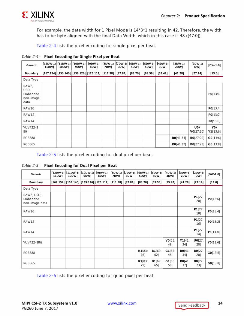
The width of the s_axis_tdata or the vid_pxl port is calculated as shown below:
Data Width = Byte aligned of (14*3*Pixel Mode)
System Interface
Interrupt System Output System interrupt output
Table 2-2: Port Values on AXI4-Stream Interface
Port Value
s_axis_tuser[6-1] 0x2A
s_axis_tuser[63-48] 0x0F00
s_axis_tdest[1:0] 0x3
Table 2-3: Port Values on Native Video Interface
Port Value
vid_di[5:0] 0x2C
vid_wc[15:0] 0x1680
vid_vc[1:0] 0x2
Table 2-1: Port Descriptions (Cont’d)
Signal name Interface Direction Description
Send Feedback
MIPI CSI-2 TX Subsystem v1.0 www.xilinx.com 14PG260 June 7, 2017
Chapter 2: Product Specification
For example, the data width for 1 Pixel Mode is 14*3*1 resulting in 42. Therefore, the width has to be byte aligned with the final Data Width, which in this case is 48 ([47:0]).
Table 2-4 lists the pixel encoding for single pixel per beat.
Table 2-5 lists the pixel encoding for dual pixel per beat.
Table 2-6 lists the pixel encoding for quad pixel per beat.
Table 2-4: Pixel Encoding for Single Pixel per Beat
Generic [12DW-1:11DW]
[11DW-1:10DW]
[10DW-1:9DW]
[9DW-1:8DW]
[8DW-1:7DW]
[7DW-1:6DW]
[6DW-1:5DW]
[5DW-1:4DW]
[4DW-1: 3DW]
[3DW-1:2DW]
[2DW-1: DW] [DW-1:0]
Boundary [167:154] [153:140] [139:126] [125:112] [111:98] [97:84] [83:70] [69:56] [55:42] [41:28] [27:14] [13:0]
Data Type
RAW8, USD, Embedded non-image data
P0[13:6]
RAW10 P0[13:4]
RAW12 P0[13:2]
RAW14 P0[13:0]
YUV422-8Bit
U0/V0[27:20]
Y0/Y1[13:6]
RGB888 R0[41:34] B0[27:20] G0[13:6]
RGB565 R0[41:37] B0[27:23] G0[13:8]
Table 2-5: Pixel Encoding for Dual Pixel per Beat
Generic [12DW-1:11DW]
[11DW-1:10DW]
[10DW-1:9DW]
[9DW-1:8DW]
[8DW-1:7DW]
[7DW-1:6DW]
[6DW-1:5DW]
[5DW-1:4DW]
[4DW-1: 3DW]
[3DW-1:2DW]
[2DW-1: DW] [DW-1:0]
Boundary [167:154] [153:140] [139:126] [125:112] [111:98] [97:84] [83:70] [69:56] [55:42] [41:28] [27:14] [13:0]
Data Type
RAW8, USD, Embedded non-image data
P1[27:20] P0[13:6]
RAW10 P1[27:18] P0[13:4]
RAW12 P1[27:16] P0[13:2]
RAW14 P1[27:14] P0[13:0]
YUV422-8Bit V0[55:48]
Y1[41:34]
U0[27:20] Y0[13:6]
RGB888 R1[83:76]
B1[69:62]
G1[55:48]
R0[41:34]
B0[27:20] G0[13:6]
RGB565 R1[83:79]
B1[69:65]
G1[55:50]
R0[41:37]
B0[27:23] G0[13:8]
Send Feedback

MIPI CSI-2 TX Subsystem v1.0 www.xilinx.com 15PG260 June 7, 2017
Chapter 2: Product Specification
Register SpaceThis section details registers available in the MIPI CSI-2 TX Subsystem. The address map is split into following regions:
• MIPI CSI-2 TX Controller core
• MIPI D-PHY core
Each IP core is given an address space of 32K. Example offset addresses from the system base address when the MIPI D-PHY registers are enabled are shown in Table 2-7.
Table 2-6: Pixel encoding for Quad Pixel per Beat
Generic [12DW-1:11DW]
[11DW-1:10DW]
[10DW-1:9DW]
[9DW-1:8DW]
[8DW-1:7DW]
[7DW-1:6DW]
[6DW-1:5DW]
[5DW-1:4DW]
[4DW-1: 3DW]
[3DW-1:2DW]
[2DW-1: DW] [DW-1:0]
Boundary [167:154] [153:140] [139:126] [125:112] [111:98] [97:84] [83:70] [69:56] [55:42] [41:28] [27:14] [13:0]
Data Type
RAW8, USD, Embedded non-image data
P3[55:48]
P2[41:34]
P1[27:20] P0[13:6]
RAW10 P3[55:46]
P2[41:32]
P1[27:18] P0[13:4]
RAW12 P3[55:44]
P2[41:30]
P1[27:16] P0[13:2]
RAW14 P3[55:42]
P2[41:28]
P1[27:14] P0[13:0]
YUV422-8Bit V2[111:104]
Y3[97:90]
U2[83:76]
Y2[69:62]
V0[55:48]
Y1[41:34]
U0[27:20] Y0[13:6]
RGB888 R3[167:160]
B3[153:146]
G3[139:132]
R2[125:118]
B2[111:104]
G2[97:90]
R1[83:76]
B1[69:62]
G1[55:48]
R0[41:34]
B0[27:20] G0[13:6]
RGB565 R3[167:163]
B3[153:149]
G3[139:134]
R2[125:121]
B2[111:107]
G2[97:92]
R1[83:79]
B1[69:65]
G1[55:50]
R0[41:37]
B0[27:23] G0[13:8]
Table 2-7: Sub-Core Address Offsets
IP Cores Offset
MIPI CSI-2 TX Controller 0x0000
MIPI D-PHY 0x1000
Send Feedback

MIPI CSI-2 TX Subsystem v1.0 www.xilinx.com 16PG260 June 7, 2017
Chapter 2: Product Specification
MIPI CSI-2 TX Controller Core RegistersTable 2-8 specifies the name, address, and description of each firmware addressable register within the MIPI CSI-2 TX controller core.
Table 2-8: MIPI CSI-2 TX Controller Core Registers
Address Offset Register Name Description
0x00 Core Configuration Core configuration options
0x04 Protocol Configuration Protocol configuration options
0x08 Reserved(1)
0x0C Reserved
0x10 Reserved
0x14 Reserved
0x18 Reserved
0x1C Reserved
0x20 Global Interrupt Enable Global interrupt enable registers
0x24 Interrupt status Interrupt status register
0x28 Interrupt enable Interrupt enable register
0x2C Reserved
0x30 Generic short packet Entry Entry for the generic short packets
0x34 Reserved
0x38 Reserved
0x3C Reserved
0x40 Reserved
0x44 Reserved
0x48 Reserved
0x4C Reserved
0x50 Reserved
0x54 Reserved
0x58 Reserved
0x5C Reserved
0x60 Reserved
0x64 Reserved
0x68 Reserved
0x6C Reserved
0x70 Reserved
0x74 Reserved
0x78 Generic Short Packet Status Generic short packet FIFO status
Send Feedback

MIPI CSI-2 TX Subsystem v1.0 www.xilinx.com 17PG260 June 7, 2017
Chapter 2: Product Specification
Core Configuration Register
The Core Configuration register is described in Table 2-9 and allows you to enable and disable the MIPI CSI-2 TX Controller core and apply a soft reset during core operation.
0x7C Reserved
Notes: 1. Access type and reset value for all the reserved bits in the registers is read-only with value 0.2. Register accesses should be word aligned and there is no support for a write strobe. WSTRB is not used internally.3. Only the lower 7 bits (6:0) of the read and write address of the AXI4-Lite interface are decoded. This means that
accessing address 0x00 and 0x80 results in reading the same address of 0x00.4. Reads and writes to addresses outside this table do not return an error.
Table 2-9: Core Configuration Register
Bits Name Reset Value Access Description
31–5 Reserved N/A N/AReservedNot used by the coreRecommended to write 0
4 Clock Mode 0x0 R/WClock mode configuration0: Continuous clock mode1: Non-continuous clock mode
3 ULPS Mode 0x0 R/WDrives the lane into ULPS mode0: Exit1: Entry
2 Controller Ready 0x1 R
Controller is ready for processingDuring soft-reset or core disable, rely on this status to ensure if the core has stopped all its activity1: Controller is Ready0: Controller is Inactive
1 Soft Reset 0x0 R/W
Soft reset to core1: Resets the ISR bits only0: Takes the core out of soft resetOnce the soft reset is released, core starts capturing new status information to ISR
Table 2-8: MIPI CSI-2 TX Controller Core Registers (Cont’d)
Address Offset Register Name Description
Send Feedback

MIPI CSI-2 TX Subsystem v1.0 www.xilinx.com 18PG260 June 7, 2017
Chapter 2: Product Specification
Protocol Configuration Register
The Protocol Configuration register is described in Table 2-10 and allows you to configure protocol specific options such as the number of lanes to be used.
0 Core Enable 0x0 R/W
1: Enables the core to receive and process packets0(1): Disables the core for operation• When disabled, the controller ends the current
transfer by resetting all internal FIFOs and registers• When enabled, the controller starts transferring the
vsync packet (a new video frame)
Notes: 1. When the Core is Disabled (Core Enable is set to 0), you can write into the registers, but the CSI2 TX Controller
captures the value only after the core is Enabled (Core Enable is set to 1). The controller also ignores the writes to the Generic Short Packet Entry Register.
Table 2-10: Protocol Configuration Register
Bits Name Reset Value Access Description
31–16 Reserved N/A N/AReservedNot used by the core
15 Line start/End Generation 0x0 R/W
Line synchronization packet generation0: Do not generate line start/end1: Generate line start/endNote: Writing this bit might have an impact from the immediate received line, after the change in the configuration.
14-13 Pixel Mode 0x0 R
Configured pixel mode0x0—1 pixel mode0x1—2 pixel mode0x3—4 pixel mode
12-5 Reserved N/A N/A Reserved
4–3 Maximum LanesNumber of lanes configured during core generation
R
Maximum lanes of the core0x0—1 Lane0x1—2 Lanes0x2—3 Lanes0x3—4 Lanes
2 Reserved N/A Reserved
Table 2-9: Core Configuration Register (Cont’d)
Bits Name Reset Value Access Description
Send Feedback
MIPI CSI-2 TX Subsystem v1.0 www.xilinx.com 19PG260 June 7, 2017
Chapter 2: Product Specification
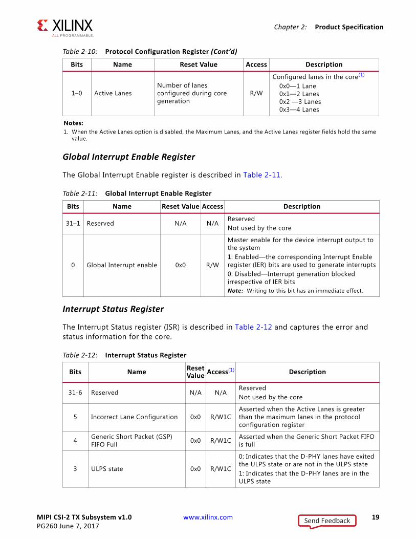
Global Interrupt Enable Register
The Global Interrupt Enable register is described in Table 2-11.
Interrupt Status Register
The Interrupt Status register (ISR) is described in Table 2-12 and captures the error and status information for the core.
1–0 Active LanesNumber of lanes configured during core generation
R/W
Configured lanes in the core(1)
0x0—1 Lane0x1—2 Lanes0x2 —3 Lanes0x3—4 Lanes
Notes: 1. When the Active Lanes option is disabled, the Maximum Lanes, and the Active Lanes register fields hold the same
value.
Table 2-11: Global Interrupt Enable Register
Bits Name Reset Value Access Description
31–1 Reserved N/A N/AReservedNot used by the core
0 Global Interrupt enable 0x0 R/W
Master enable for the device interrupt output to the system1: Enabled—the corresponding Interrupt Enable register (IER) bits are used to generate interrupts0: Disabled—Interrupt generation blocked irrespective of IER bitsNote: Writing to this bit has an immediate effect.
Table 2-12: Interrupt Status Register
Bits Name ResetValue Access(1) Description
31-6 Reserved N/A N/AReservedNot used by the core
5 Incorrect Lane Configuration 0x0 R/W1CAsserted when the Active Lanes is greater than the maximum lanes in the protocol configuration register
4 Generic Short Packet (GSP) FIFO Full 0x0 R/W1C Asserted when the Generic Short Packet FIFO
is full
3 ULPS state 0x0 R/W1C
0: Indicates that the D-PHY lanes have exited the ULPS state or are not in the ULPS state1: Indicates that the D-PHY lanes are in the ULPS state
Table 2-10: Protocol Configuration Register (Cont’d)
Bits Name Reset Value Access Description
Send Feedback

MIPI CSI-2 TX Subsystem v1.0 www.xilinx.com 20PG260 June 7, 2017
Chapter 2: Product Specification
Interrupt Enable Register
The Interrupt Enable register (IER) is described in Table 2-13 and allows you to selectively generate an interrupt at the output port for each error/status bit in the ISR. An IER bit set to 0 does not inhibit an error/status condition from being captured, but inhibits it from generating an interrupt.
2 Line Buffer Full 0x0 R/W1C Asserted when the Line Buffer is Full
1 Unsupported/Reserved Data Type 0x0 R/W1C
Asserted when the unsupported or the reserved data types are seen in the generic short packet request
0 Pixel Data Underrun 0x0 R/W1C Asserted when the core starves for pixel data during the packet transmission
Notes: 1. W1C = Write 1 to clear.
Table 2-13: Interrupt Enable Register
Bits Name Reset Value Access Description
31-6 Reserved N/A N/AReservedNot used by the core
5 Incorrect Lane Configuration Enable 0x0 R/W Generate interrupt on incorrect lane configuration
4 Generic Short Packet (GSP) FIFO Full Enable 0x0 R/W Generate interrupt on GSP
FIFO full
3 ULPS State Enable 0x0 R/W Generate interrupt on ULPS state
2 Line Buffer Full Enable 0x0 R/W Generate interrupt when the line buffer is full
1 Unsupported/Reserved Data Type Enable 0x0 R/WGenerate interrupt on unsupported or reserved data type
0 Pixel Data Underrun Enable 0x0 R/W Generate interrupt on the pixel data underrun condition
Table 2-12: Interrupt Status Register (Cont’d)
Bits Name ResetValue Access(1) Description
Send Feedback

MIPI CSI-2 TX Subsystem v1.0 www.xilinx.com 21PG260 June 7, 2017
Chapter 2: Product Specification
Generic Short Packet Entry Register
The Generic Short Packet Entry register is described in Table 2-14. Only generic short packets are supported (data types from 0x08 to 0x0F).
Generic Short Packet Status Register
The Generic Short Packet Status register is described in Table 2-15. This register indicates the number of generic short packets (GSP) that can be written safely.
MIPI D-PHY RegistersThe MIPI D-PHY registers are available when D-PHY Register Interface is selected in Vivado IDE. For details about MIPI D-PHY registers, see the MIPI D-PHY LogiCORE IP Product Guide (PG202) [Ref 3].
Table 2-14: Generic Short Packet Entry Register
Bits Name Reset Value Access Description
31–24 Reserved N/A N/A Reserved
23–16 Byte-1 0x0 R/W Byte 1 of the short packet
15–8 Byte-0 0x0 R/W Byte 0 of the short packet
7–6 VC 0x0 R/W VC value of the short packet
5–0 Data type 0x0 R/W Short packet data type
Table 2-15: Clock Lane Information Register
Bits Name Reset Value Access Description
31–5 Reserved N/A N/A Reserved
5–0 Generic Short Packet Vacancy 0x20 R
Number of generic short packets that can be safely written to the Generic Short Packet FIFO, before it goes full
Send Feedback

MIPI CSI-2 TX Subsystem v1.0 www.xilinx.com 22PG260 June 7, 2017
Chapter 3
Designing with the SubsystemThis chapter includes guidelines and additional information to facilitate designing with the subsystem.
General Design GuidelinesThe subsystem fits into a image sensor pipe transmission path. The input to the subsystem must be connected to a AXI4-S stream source or Native stream source which generates the pixel data. The output of the subsystem is a MIPI complaint serial data. Because the MIPI protocol does not allow throttling on the output interface (PPI), the module connected to the output of this subsystem should have sufficient bandwidth for the data generated by the image sensor.
The Protocol Configuration Register [1:0] can be used to dynamically configure the active lanes used by the subsystem using the following guidelines:
1. Program the required lanes in the Protocol Configuration register only when the following conditions are met:
a. “Enable Active Lanes” is set in the Vivado IDE
b. There is no ongoing transfer on the PPI and all the data lanes are in the stop-state
2. Do not send the new updated lanes traffic until the read from Protocol Configuration registers reflects the new value.
Shared LogicShared Logic provides a flexible architecture that works both as a stand-alone subsystem and as part of a larger design with one of more subsystem instances. This minimizes the amount of HDL modifications required, but at the same time retains the flexibility of the subsystem.
Shared logic in the CSI-2 TX Subsystem allows you to share MMCMs and PLLs with multiple instances of the CSI-2 TX Subsystem within the same I/O bank.
Send Feedback

MIPI CSI-2 TX Subsystem v1.0 www.xilinx.com 23PG260 June 7, 2017
Chapter 3: Designing with the Subsystem
There is a level of hierarchy called <component_name>_support. Figure 3-1 and Figure 3-2 show two hierarchies where the shared logic is either contained in the subsystem or in the example design. In these figures, <component_name> is the name of the generated subsystem. The difference between the two hierarchies is the boundary of the subsystem. It is controlled using the Shared Logic option in the Vivado IDE Shared Logic tab for the MIPI CSI-2 TX Subsystem. The shared logic comprises an MMCM, a PLL and some BUFGs (maximum of 4).
Shared Logic in the CoreSelecting Shared Logic in the Core implements the subsystem with the MMCM and PLL inside the subsystem to generate all the clocking requirement of the PHY layer.
Select Include Shared Logic in Core if:
• You do not require direct control over the MMCM and PLL generated clocks
X-Ref Target - Figure 3-1
Figure 3-1: Shared Logic Included in the SubsystemX-Ref Target - Figure 3-2
Figure 3-2: Shared Logic Outside Subsystem
<Component Name>_exdes
<Component Name>_core
<Component Name>_core
Send Feedback

MIPI CSI-2 TX Subsystem v1.0 www.xilinx.com 24PG260 June 7, 2017
Chapter 3: Designing with the Subsystem
• You want to manage multiple customizations of the subsystem for multi-subsystem designs
• This is the first MIPI CSI-2 TX Subsystem in a multi-subsystem system
These components are included in the subsystem, and their output ports are also provided as subsystem outputs.
Shared Logic in Example DesignThe MMCMs and PLLs are outside this subsystem instance.
Select Include Shared Logic in example design if:
• This is the second MIPI CSI-2 TX Subsystem instance in a multi-subsystem design
• You only want to manage one customization of the MIPI CSI-2 TX Subsystem in your design
• You want direct access to the input clocks
To fully utilize the MMCM and PLL, customize one MIPI CSI-2 TX Subsystem with shared logic in the subsystem and one with shared logic in the example design. You can connect the MMCM/PLL outputs from the first MIPI CSI-2 TX Subsystem to the second subsystem.
If you want fine control you can select Include Shared Logic in example design and base your own logic on the shared logic produced in the example design.
Figure 3-3 shows the sharable resource connections from the MIPI CSI-2 TX Subsystem with shared logic included (MIPI_ CSI_SS_Master) to the instance of another MIPI CSI-2 TX Subsystem without shared logic (MIPI_ CSI_SS_Slave00 and MIPI_ CSI_SS_Slave01).
I/O PlanningThe MIPI D-PHY core provides an I/O planner feature for I/O selection. You can select any I/O for the clock and data lanes in the TX core configuration for the selected HP I/O bank.
Eight D-PHY IP cores can be implemented per I/O bank due to BITSLICE and BITSLICE_CONTROL instances in the UltraScale+ devices.
Send Feedback

MIPI CSI-2 TX Subsystem v1.0 www.xilinx.com 25PG260 June 7, 2017
Chapter 3: Designing with the Subsystem
Note: The master and slave subsystems should be configured with the same line rate when sharing MMCM/PLL resources.
X-Ref Target - Figure 3-3
Figure 3-3: Shared Logic in the Example Design
Send Feedback

MIPI CSI-2 TX Subsystem v1.0 www.xilinx.com 26PG260 June 7, 2017
Chapter 3: Designing with the Subsystem
ClockingThe subsystem clocks are described in Table 3-1.
The register interface also works on the s_axis_aclk core clock. Selection of s_axis_aclk is based on TxByteClk.
When the effective pixel width is less than or equal to (<=) 32, the s_axis_clk should be selected such that the input bandwidth is at least 20-30% more than the output bandwidth. For example, s_axis_aclk*Pixel_width*Pixel_Mode > TxByteClk*No_Lanes*8.
Where s_axis_aclk*Pixel_width*Pixel_Mode is approximately equal to 1.2 or 1.3 times of (TxByteClk*No_Lanes*8).
When the effective pixel is greater than (>) 32, the s_axis_aclk should be selected such that the input bandwidth is at least more than 2-3 times the output bandwidth. For example, s_axis_aclk*Pixel_width*Pixel_Mode > TxByteClk*No_Lanes*8.
Where s_axis_aclk*Pixel_width*Pixel_Mode is approximately equal to 2 or 3 times of (TxByteClk*No_Lanes*8).
Note: If the above relations are not met, the MIPI CSI-2 TX controller will report an under-run condition.
Note: For data type interleaving with native video interface, select data types with similar pixel widths to avoid under-run or line buffer full. For example, RAW8, RAW10.
Table 3-1: Subsystem Clocks
Clock Name Description
txByteClkhs Clock used to transfer on the PPI interface signals
s_axis_aclk Clock used to perform all core operation blocks
Table 3-2: Clocking Examples for Different Combinations
Data Type Line Rate (Mb/s) txByteclkhs(MHz) Lanes Pixel Mode s_axis_aclk(MHz)
RAW8 1200 150 1 1 180
RAW10 900 112.5 2 2 117
RAW12 1000 125 3 4 125
RGB888 800 100 4 4 100
RAW14 500 62.5 2 2 42.8
RGB565 1000 125 1 2 40
YUV-422-8 Bit 1500 187.5 3 4 140.6
Send Feedback

MIPI CSI-2 TX Subsystem v1.0 www.xilinx.com 27PG260 June 7, 2017
Chapter 3: Designing with the Subsystem
ResetsThe MIPI CSI-2 Transmitter Controller has one hard reset (s_axis_aresetn) and one register based reset (soft reset).
• s_axis_aresetn: All the core logic blocks reset to power-on conditions including registers.
• The soft reset resets the Interrupt Status register (ISR) of MIPI CSI-2 TX Controller and does not affect the core processing.
The subsystem has one external reset port:
• s_axis_aresetn: Active-Low reset for the subsystem blocks
The duration of s_axis_aresetn should be a minimum of 40 dphy_clk_200M cycles to propagate the reset throughout the system.
The reset sequence is shown in Figure 3-4.
Table 3-3 summarizes all resets available to the MIPI CSI-2 TX Subsystem and the components affected by them.
Note: The effect of each reset (s_axis_aresetn) is determined by the ports of the sub-cores to which they are connected. See the individual sub-core product guides for the effect of each reset signal.
X-Ref Target - Figure 3-4
Figure 3-4: Shared Logic Outside Subsystem
Table 3-3: Subsystem Components
Sub-core s_axis_aresetn
MIPI CSI-2 TX Controller Connected to s_axi_aresetn core port
MIPI DPHY Inverted signal connected to core_rst port
AXI Crossbar Connected to aresetn port
Send Feedback

MIPI CSI-2 TX Subsystem v1.0 www.xilinx.com 28PG260 June 7, 2017
Chapter 3: Designing with the Subsystem
Protocol Description
Programming SequenceThis section contains the programming sequence for the subsystem. Program and enable the components of subsystem in the following order:
1. MIPI CSI-2 TX Controller
2. MIPI D-PHY (if register interface is enabled)
Address Map ExampleTable 3-4 shows an example based on a subsystem base address of 0x44A0_0000 (32 bits) when the MIPI D-PHY register interface is enabled.
MIPI CSI-2 TX Controller Core ProgrammingThe MIPI CSI-2 TX Controller programming sequence is as follows. Figure 3-6, Figure 3-6, and Figure 3-7 show a graphical representation of the sequence:
1. Configure the registers and enable the core
a. Read the Core Configuration Register to ensure that the controller ready bit is set to 1, before enabling the core anytime (for example, after reset or after disabling the core).
b. Configure the required configuration through register programming.
c. Enable the core and send video stream on input interface.
d. All along this sequence, either continuously poll or wait for external interrupt (if enabled) and read interrupt status register for any errors or status reported.
2. Disabling and re-enabling the core
Table 3-4: Address Map Example
Core Base address
MIPI CSI-2 TX Controller 0x0000
MIPI D-PHY 0x1000
X-Ref Target - Figure 3-5
Figure 3-5: Core Programming Sequence - Enable the core
Send Feedback

MIPI CSI-2 TX Subsystem v1.0 www.xilinx.com 29PG260 June 7, 2017
Chapter 3: Designing with the Subsystem
° Disable the core using the Core Configuration Register (set the Core Enable bit to 0).
° Wait until the controller ready bit is set in the Core Configuration Register.
° Re-enable the core (set the Core Enable bit to 1)
3. ULPS Entry and ULPS Exit
° Drive the PHY Lanes to ULPS Mode, write 1 into the Core Configuration Register (set the ULPS Mode bit to 1).
° Corresponding PPI Signals are driven to the PHY (txrequestesc , txulpsesc) for the entry into the ULPS State.
° After the PHY Lanes have entered into the ULPS State (ulpsactivenot goes low) the Interrupt Status register is updated with the corresponding status.
° Exit the ULPS state, write 0 into the Core Configuration Register (set the ULPS Mode bit to 0).
° Corresponding PPI Signal is driven to the PHY (txulpsexit) for exiting from the ULPS State.
° PPI deasserts the txrequestesc after a millisecond of deassertion of the ulpsactivenot signal. The ULPS exit is indicated through the Interrupt Status register.
MIPI D-PHY IP Core Programming
See the MIPI D-PHY LogiCORE IP Product Guide (PG202) [Ref 3] for MIPI D-PHY IP core programming details.
X-Ref Target - Figure 3-6
Figure 3-6: Core Programming Sequence - Disable and Re-enable the Core
X-Ref Target - Figure 3-7
Figure 3-7: Core Programming Sequence - ULPS Entry and ULPS Exit
Send Feedback
MIPI CSI-2 TX Subsystem v1.0 www.xilinx.com 30PG260 June 7, 2017
Chapter 4
Design Flow StepsThis chapter describes customizing and generating the subsystem, constraining the subsystem, and the simulation, synthesis and implementation steps that are specific to this subsystem. More detailed information about the standard Vivado® design flows and the IP integrator can be found in the following Vivado Design Suite user guides:
• Vivado Design Suite User Guide: Designing IP Subsystems using IP Integrator (UG994) [Ref 8]
• Vivado Design Suite User Guide: Designing with IP (UG896) [Ref 9]
• Vivado Design Suite User Guide: Getting Started (UG910) [Ref 10]
• Vivado Design Suite User Guide: Logic Simulation (UG900) [Ref 11]
Customizing and Generating the SubsystemThis section includes information about using Xilinx tools to customize and generate the subsystem in the Vivado Design Suite.
If you are customizing and generating the subsystem in the Vivado IP integrator, see the Vivado Design Suite User Guide: Designing IP Subsystems using IP Integrator (UG994) [Ref 8] for detailed information. IP integrator might auto-compute certain configuration values when validating or generating the design. To check whether the values do change, see the description of the parameter in this chapter. To view the parameter value, run the validate_bd_design command in the Tcl console.
You can customize the IP for use in your design by specifying values for the various parameters associated with the subsystem using the following steps:
1. Select the IP from the Vivado IP catalog.
2. Double-click the selected IP or select the Customize IP command from the toolbar or right-click menu.
Send Feedback

MIPI CSI-2 TX Subsystem v1.0 www.xilinx.com 31PG260 June 7, 2017
Chapter 4: Design Flow Steps
For details, see the Vivado Design Suite User Guide: Designing with IP (UG896) [Ref 9] and the Vivado Design Suite User Guide: Getting Started (UG910) [Ref 10].
Note: Figures in this chapter are illustrations of the Vivado Integrated Design Environment (IDE). The layout depicted here might vary from the current version.
The subsystem configuration screen is shown in Figure 4-1.
Component Name: The Component Name is used as the name of the top-level wrapper file for the subsystem. The underlying netlist still retains its original name. Names must begin with a letter and must be composed from the following characters: a through z, 0 through 9, and “_”. The default is mipi_csi2_tx_subsystem_0.
X-Ref Target - Figure 4-1
Figure 4-1: Subsystem Customization Screen-Configuration Tab Page
Send Feedback

MIPI CSI-2 TX Subsystem v1.0 www.xilinx.com 32PG260 June 7, 2017
Chapter 4: Design Flow Steps
Configuration TabThe Configuration tab page provides core related configuration parameters.
Input Video Interface: Select the video interface used to accept pixel data. Values are AXI4S and Native.
Input Pixels per beat: Select the number of input pixels per clock on input interface. Values are 1 (single pixel), 2 (dual pixel), or 4(quad pixel).
Line Buffer Depth: Select the depth of internal RAM based on the bandwidth requirement such that the line buffer does not overflow. Values are 128, 256, 512, 1024, 2048, 4096, 8192 or 16384.
CSI Lanes: Select the maximum number of D-PHY lanes for this subsystem instance. Values are 1, 2, 3, or 4.
CRC Generation Logic: When set, CRC computation is performed and appended to the payload data.
Enable Active Lanes: When set, the core supports the dynamic configuration of the number of active lanes from the maximum number of lanes selected during core generation using the parameter CSI Lanes. For example, when CSI Lanes is set to 3, the number of active lanes can be programmed using the protocol configuration register to be 1,2 or 3. The core reports an error when the active lanes setting is greater than the serial lanes setting through the interrupt status register, bit 5.
Line Rate (Mb/s): Selects the line rate for the MIPI D-PHY core. Maximum line rate for the UltraScale+ devices is 1500 Mb/s, and for the 7 Series is 1250 Mb/s.
Enable AXI-4 Lite Register I/F: Select to enable the register interface for the MIPI D-PHY core.
Infer OBUFTDS for 7 series HS outputs
Select this option to infer OBUFTDS for HS outputs.
Note: This option is available only for 7 Series D-PHY TX configuration. It is recommended to use this option for D-PHY compatible solution based on resistive circuit. For details, see D-PHY Solutions (XAPP894) [Ref 15].
Send Feedback

MIPI CSI-2 TX Subsystem v1.0 www.xilinx.com 33PG260 June 7, 2017
Chapter 4: Design Flow Steps
Shared Logic TabThe Shared Logic tab page provides shared logic inclusion parameters. The subsystem shared logic configuration screen is shown in Figure 4-2.
Shared Logic: Select whether the MMCM and PLL are included in the core or in the example design. Values are:
• Include Shared Logic in core
• Include Shared Logic in example design
X-Ref Target - Figure 4-2
Figure 4-2: Subsystem Customization Screen-Shared Logic Tab Page
Send Feedback
MIPI CSI-2 TX Subsystem v1.0 www.xilinx.com 34PG260 June 7, 2017
Chapter 4: Design Flow Steps
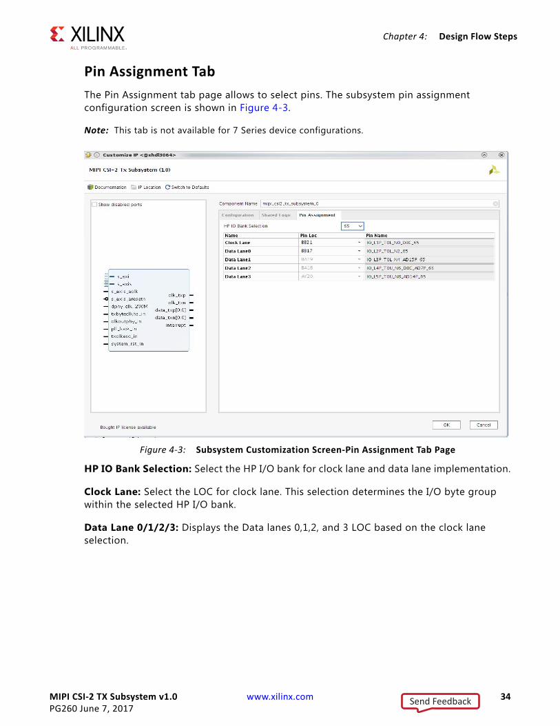
Pin Assignment TabThe Pin Assignment tab page allows to select pins. The subsystem pin assignment configuration screen is shown in Figure 4-3.
Note: This tab is not available for 7 Series device configurations.
HP IO Bank Selection: Select the HP I/O bank for clock lane and data lane implementation.
Clock Lane: Select the LOC for clock lane. This selection determines the I/O byte group within the selected HP I/O bank.
Data Lane 0/1/2/3: Displays the Data lanes 0,1,2, and 3 LOC based on the clock lane selection.
X-Ref Target - Figure 4-3
Figure 4-3: Subsystem Customization Screen-Pin Assignment Tab Page
Send Feedback
MIPI CSI-2 TX Subsystem v1.0 www.xilinx.com 35PG260 June 7, 2017
Chapter 4: Design Flow Steps
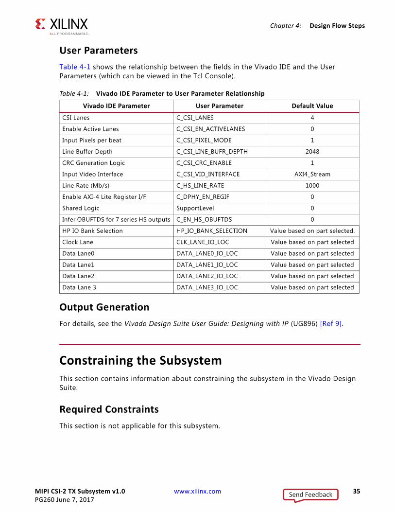
User ParametersTable 4-1 shows the relationship between the fields in the Vivado IDE and the User Parameters (which can be viewed in the Tcl Console).
Output GenerationFor details, see the Vivado Design Suite User Guide: Designing with IP (UG896) [Ref 9].
Constraining the SubsystemThis section contains information about constraining the subsystem in the Vivado Design Suite.
Required ConstraintsThis section is not applicable for this subsystem.
Table 4-1: Vivado IDE Parameter to User Parameter Relationship
Vivado IDE Parameter User Parameter Default Value
CSI Lanes C_CSI_LANES 4
Enable Active Lanes C_CSI_EN_ACTIVELANES 0
Input Pixels per beat C_CSI_PIXEL_MODE 1
Line Buffer Depth C_CSI_LINE_BUFR_DEPTH 2048
CRC Generation Logic C_CSI_CRC_ENABLE 1
Input Video Interface C_CSI_VID_INTERFACE AXI4_Stream
Line Rate (Mb/s) C_HS_LINE_RATE 1000
Enable AXI-4 Lite Register I/F C_DPHY_EN_REGIF 0
Shared Logic SupportLevel 0
Infer OBUFTDS for 7 series HS outputs C_EN_HS_OBUFTDS 0
HP IO Bank Selection HP_IO_BANK_SELECTION Value based on part selected.
Clock Lane CLK_LANE_IO_LOC Value based on part selected
Data Lane0 DATA_LANE0_IO_LOC Value based on part selected
Data Lane1 DATA_LANE1_IO_LOC Value based on part selected
Data Lane2 DATA_LANE2_IO_LOC Value based on part selected
Data Lane 3 DATA_LANE3_IO_LOC Value based on part selected
Send Feedback

MIPI CSI-2 TX Subsystem v1.0 www.xilinx.com 36PG260 June 7, 2017
Chapter 4: Design Flow Steps
Device, Package, and Speed Grade SelectionsThis section is not applicable for this subsystem.
Clock FrequenciesSee Clocking.
Clock ManagementThe MIPI CSI-2 TX Subsystem sub-core MIPI D-PHY uses an MMCM to generate the general interconnect clocks, and the PLL is used to generate the serial clock and parallel clocks for the PHY. The input to the MMCM is constrained as shown in Clock Frequencies section of MIPI D-PHY LogiCORE IP Product Guide (PG202) [Ref 3]. No additional constraints are required for the clock management.
Clock PlacementThis section is not applicable for this subsystem.
BankingThe MIPI CSI-2 TX Subsystem provides the Pin Assignment Tab option to select the HP I/O bank. Clock lane and data lane(s) are implemented on the selected I/O bank BITSLICE(s).
Transceiver PlacementThis section is not applicable for this subsystem.
I/O Standard and PlacementThe MIPI standard serial I/O ports should use MIPI_DPHY_DCI for the I/O standard in the XDC file for UltraScale+ family. The LOC and I/O standards must be specified in the XDC file for all input and output ports of the design. The MIPI CSI-2 TX Subsystem MIPI D-PHY sub-core generates the I/O pin LOC for the pins that are selected during IP customization for UltraScale+ designs. No I/O pin LOC are provided for 7 Series MIPI D-PHY IP designs. You have to manually select the clock capable I/O for 7 series TX clock lane and restrict the I/O selection within the I/O bank for MIPI D-PHY TX.
It is recommended to select the I/O bank with VRP pin connected for UltraScale+ MIPI D-PHY TX IP core. If VRP pin is present in other I/O bank in the same I/O column of the device the following DCI_CASCADE XDC constraint should be used. For example, I/O bank 65 has a VPR pin and the D-PHY TX IP is using the I/O bank 66.
set_property DCI_CASCADE {66} [get_iobanks 65]
Send Feedback

MIPI CSI-2 TX Subsystem v1.0 www.xilinx.com 37PG260 June 7, 2017
Chapter 4: Design Flow Steps
SimulationFor comprehensive information about Vivado simulation components, as well as information about using supported third-party tools, see the Vivado Design Suite User Guide: Logic Simulation (UG900) [Ref 11].
Synthesis and ImplementationFor details about synthesis and implementation, see the Vivado Design Suite User Guide: Designing with IP (UG896) [Ref 9].
Send Feedback
MIPI CSI-2 TX Subsystem v1.0 www.xilinx.com 38PG260 June 7, 2017
Appendix A
Verification, Compliance, and Interoperability
The MIPI CSI-2 TX Subsystem has been verified using both simulation and hardware testing. A highly parameterizable transaction-based simulation test suite has been used to verify the subsystem. The tests include:
• Different lane combinations and line rates
• High-Speed Data transmission with short/long packets, different virtual channels and different data types.
• All possible interleaving cases (data type and virtual channel)
• All possible output pixel, data type combinations.
• Register read and write access
Hardware ValidationThe MIPI CSI-2 TX Subsystem is tested in hardware for functionality, performance, and reliability using Xilinx® evaluation platforms. The MIPI CSI-2 TX Subsystem verification test suites for all possible modules are continuously being updated to increase test coverage across the range of possible parameters for each individual module.
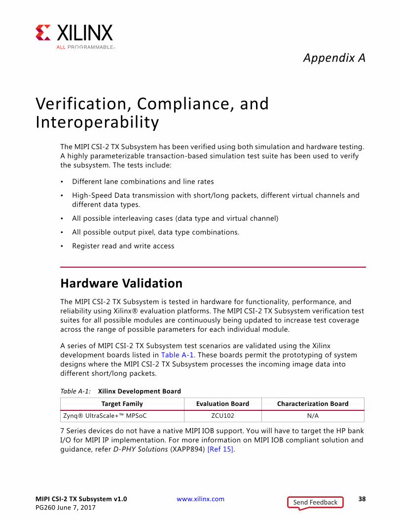
A series of MIPI CSI-2 TX Subsystem test scenarios are validated using the Xilinx development boards listed in Table A-1. These boards permit the prototyping of system designs where the MIPI CSI-2 TX Subsystem processes the incoming image data into different short/long packets.
7 Series devices do not have a native MIPI IOB support. You will have to target the HP bank I/O for MIPI IP implementation. For more information on MIPI IOB compliant solution and guidance, refer D-PHY Solutions (XAPP894) [Ref 15].
Table A-1: Xilinx Development Board
Target Family Evaluation Board Characterization Board
Zynq® UltraScale+™ MPSoC ZCU102 N/A
Send Feedback

MIPI CSI-2 TX Subsystem v1.0 www.xilinx.com 39PG260 June 7, 2017
Appendix B
DebuggingThis appendix includes details about resources available on the Xilinx Support website and debugging tools.
TIP: If the IP generation halts with an error, there might be a license issue. See License Checkers in Chapter 1 for more details.
Finding Help on Xilinx.comTo help in the design and debug process when using the MIPI CSI-2 Transmit Subsystem, the Xilinx Support web page contains key resources such as product documentation, release notes, answer records, information about known issues, and links for obtaining further product support.
DocumentationThis product guide is the main document associated with the MIPI CSI-2 Transmit Subsystem. This guide, along with documentation related to all products that aid in the design process, can be found on the Xilinx Support web page or by using the Xilinx Documentation Navigator.
Download the Xilinx Documentation Navigator from the Downloads page. For more information about this tool and the features available, open the online help after installation.
Answer Records Answer Records include information about commonly encountered problems, helpful information on how to resolve these problems, and any known issues with a Xilinx product. Answer Records are created and maintained daily ensuring that users have access to the most accurate information available.
Send Feedback

MIPI CSI-2 TX Subsystem v1.0 www.xilinx.com 40PG260 June 7, 2017
Appendix B: Debugging
Answer Records for this subsystem can be located by using the Search Support box on the main Xilinx support web page. To maximize your search results, use proper keywords such as:
• Product name
• Tool message(s)
• Summary of the issue encountered
A filter search is available after results are returned to further target the results.
Master Answer Record for the MIPI CSI-2 Transmit Subsystem
AR: 67896
Technical SupportXilinx provides technical support at the Xilinx Support web page for this IP product when used as described in the product documentation. Xilinx cannot guarantee timing, functionality, or support if you do any of the following:
• Implement the solution in devices that are not defined in the documentation.
• Customize the solution beyond that allowed in the product documentation.
• Change any section of the design labeled DO NOT MODIFY.
Xilinx provides premier technical support for customers encountering issues that require additional assistance.
To contact Xilinx Technical Support, navigate to the Xilinx Support web page.
Debug ToolsThere are many tools available to address MIPI CSI-2 Transmit Subsystem design issues. It is important to know which tools are useful for debugging various situations.
Vivado Design Suite Debug FeatureThe Vivado® Design Suite debug feature inserts logic analyzer and virtual I/O cores directly into your design. The debug feature also allows you to set trigger conditions to capture application and integrated block port signals in hardware. Captured signals can then be analyzed. This feature in the Vivado IDE is used for logic debugging and validation of a design running in Xilinx devices.
Send Feedback

MIPI CSI-2 TX Subsystem v1.0 www.xilinx.com 41PG260 June 7, 2017
Appendix B: Debugging
The Vivado logic analyzer is used with the logic debug IP cores, including:
• ILA 2.0 (and later versions)
• VIO 2.0 (and later versions)
See the Vivado Design Suite User Guide: Programming and Debugging (UG908) [Ref 13].
Hardware DebugHardware issues can range from link bring-up to problems seen after hours of testing. This section provides debug steps for common issues. The Vivado debug feature is a valuable resource to use in hardware debug. The signal names mentioned in the following individual sections can be probed using the debug feature for debugging the specific problems.
General Checks• Ensure MIPI DPHY and MIPI CSI-2 TX Controller cores are in the enable state by reading
the registers.
• Ensure Incorrect Lane Configuration is not set in the MIPI CSI-2 TX Controller Interrupt status register.
• Ensure line buffer full condition is not set in the MIPI CSI-2 TX Controller Interrupt Status register.
• Ensure Pixel Data Under-run is not set in the MIPI CSI-2 TX Controller Interrupt Status register.
• Ensure GSP FIFO Full is not set in the MIPI CSI-2 TX Controller Interrupt Status register.
Note: In case, you encounter any errors, disable and re-enable the core to clear any stale data stored in the buffers.
Interface Debug
AXI4-Lite InterfacesRead from a register that does not have all 0s as a default to verify that the interface is functional. See Figure B-1 for a read timing diagram. Output s_axi_arready asserts when the read address is valid, and output s_axi_rvalid asserts when the read data/response is valid. If the interface is unresponsive, ensure that the following conditions are met:
• The lite_aclk inputs are connected and toggling.
• The interface is not being held in reset, and lite_aresetn is an active-Low reset.
Send Feedback

MIPI CSI-2 TX Subsystem v1.0 www.xilinx.com 42PG260 June 7, 2017
Appendix B: Debugging
• The main subsystem clocks are toggling and that the enables are also asserted.
• If the simulation has been run, verify in simulation and/or a debug feature capture that the waveform is correct for accessing the AXI4-Lite interface.
AXI4-Stream InterfacesIf data is not being transmitted or received, check the following conditions:
• If transmit <interface_name>_tready is stuck Low following the <interface_name>_tvalid input being asserted, the subsystem cannot send data.
• If the receive <interface_name>_tvalid is stuck Low, the subsystem is not receiving data.
• Check that the s_axis_aclk and dphy_clk_200M inputs are connected and toggling.
• Check subsystem configuration.
• Ensure “line buffer full” condition not getting reported in subsystem Interrupt Status register.
X-Ref Target - Figure B-1
Figure B-1: AXI4-Lite Timing
X-Ref Target - Figure B-2
Figure B-2: AXI4-Stream Timing
Send Feedback
MIPI CSI-2 TX Subsystem v1.0 www.xilinx.com 43PG260 June 7, 2017
Appendix B: Debugging
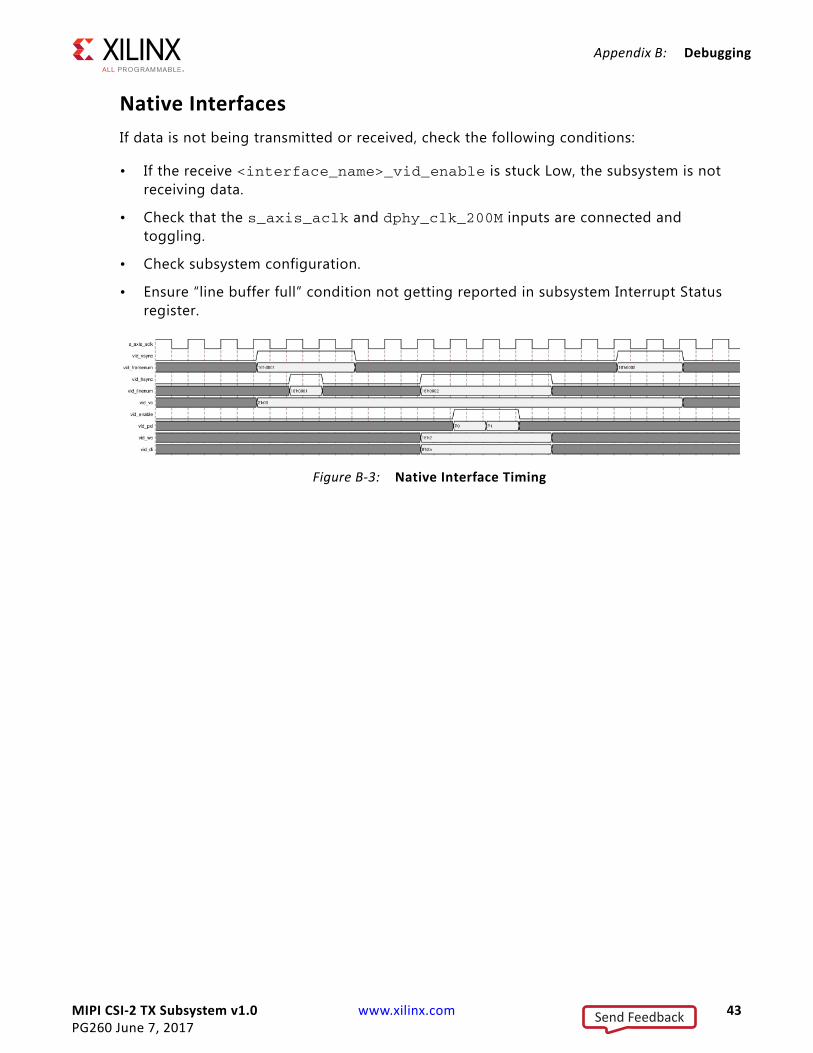
Native InterfacesIf data is not being transmitted or received, check the following conditions:
• If the receive <interface_name>_vid_enable is stuck Low, the subsystem is not receiving data.
• Check that the s_axis_aclk and dphy_clk_200M inputs are connected and toggling.
• Check subsystem configuration.
• Ensure “line buffer full” condition not getting reported in subsystem Interrupt Status register.
X-Ref Target - Figure B-3
Figure B-3: Native Interface Timing
Send Feedback
MIPI CSI-2 TX Subsystem v1.0 www.xilinx.com 44PG260 June 7, 2017
Appendix C
Additional Resources and Legal Notices
Xilinx ResourcesFor support resources such as Answers, Documentation, Downloads, and Forums, see Xilinx Support.
ReferencesThese documents provide supplemental material useful with this product guide:
1. MIPI Alliance Standard for Camera Serial Interface CSI-2: mipi.org/specifications/camera-interface#CSI2
2. AXI4-Stream Video IP and System Design Guide (UG934)
3. MIPI D-PHY LogiCORE IP Product Guide (PG202)
4. AXI Interconnect LogiCORE IP Product Guide (PG059)
5. AXI IIC Bus Interface v2.0 LogiCORE IP Product Guide (PG090)
6. MIPI Alliance Physical Layer Specifications, D-PHY Specification: http://mipi.org/specifications/physical-layer#D-PHY Specification
7. Vivado Design Suite: AXI Reference Guide (UG1037)
8. Vivado Design Suite User Guide: Designing IP Subsystems using IP Integrator (UG994)
9. Vivado Design Suite User Guide: Designing with IP (UG896)
10. Vivado Design Suite User Guide: Getting Started (UG910)
11. Vivado Design Suite User Guide: Logic Simulation (UG900)
12. ISE to Vivado Design Suite Migration Guide (UG911)
13. Vivado Design Suite User Guide: Programming and Debugging (UG908)
14. Vivado Design Suite User Guide: Implementation (UG904)
15. D-PHY Solutions (XAPP894)
Send Feedback

MIPI CSI-2 TX Subsystem v1.0 www.xilinx.com 45PG260 June 7, 2017
Appendix C: Additional Resources and Legal Notices
Revision HistoryThe following table shows the revision history for this document.
Please Read: Important Legal NoticesThe information disclosed to you hereunder (the “Materials”) is provided solely for the selection and use of Xilinx products. To the maximum extent permitted by applicable law: (1) Materials are made available “AS IS” and with all faults, Xilinx hereby DISCLAIMS ALL WARRANTIES AND CONDITIONS, EXPRESS, IMPLIED, OR STATUTORY, INCLUDING BUT NOT LIMITED TO WARRANTIES OF MERCHANTABILITY, NON-INFRINGEMENT, OR FITNESS FOR ANY PARTICULAR PURPOSE; and (2) Xilinx shall not be liable (whether in contract or tort, including negligence, or under any other theory of liability) for any loss or damage of any kind or nature related to, arising under, or in connection with, the Materials (including your use of the Materials), including for any direct, indirect, special, incidental, or consequential loss or damage (including loss of data, profits, goodwill, or any type of loss or damage suffered as a result of any action brought by a third party) even if such damage or loss was reasonably foreseeable or Xilinx had been advised of the possibility of the same. Xilinx assumes no obligation to correct any errors contained in the Materials or to notify you of updates to the Materials or to product specifications. You may not reproduce, modify, distribute, or publicly display the Materials without prior written consent. Certain products are subject to the terms and conditions of Xilinx’s limited warranty, please refer to Xilinx’s Terms of Sale which can be viewed at https://www.xilinx.com/legal.htm#tos; IP cores may be subject to warranty and support terms contained in a license issued to you by Xilinx. Xilinx products are not designed or intended to be fail-safe or for use in any application requiring fail-safe performance; you assume sole risk and liability for use of Xilinx products in such critical applications, please refer to Xilinx’s Terms of Sale which can be viewed at https://www.xilinx.com/legal.htm#tos.AUTOMOTIVE APPLICATIONS DISCLAIMERAUTOMOTIVE PRODUCTS (IDENTIFIED AS “XA” IN THE PART NUMBER) ARE NOT WARRANTED FOR USE IN THE DEPLOYMENT OF AIRBAGS OR FOR USE IN APPLICATIONS THAT AFFECT CONTROL OF A VEHICLE (“SAFETY APPLICATION”) UNLESS THERE IS A SAFETY CONCEPT OR REDUNDANCY FEATURE CONSISTENT WITH THE ISO 26262 AUTOMOTIVE SAFETY STANDARD (“SAFETY DESIGN”). CUSTOMER SHALL, PRIOR TO USING OR DISTRIBUTING ANY SYSTEMS THAT INCORPORATE PRODUCTS, THOROUGHLY TEST SUCH SYSTEMS FOR SAFETY PURPOSES. USE OF PRODUCTS IN A SAFETY APPLICATION WITHOUT A SAFETY DESIGN IS FULLY AT THE RISK OF CUSTOMER, SUBJECT ONLY TO APPLICABLE LAWS AND REGULATIONS GOVERNING LIMITATIONS ON PRODUCT LIABILITY.© Copyright 2016-2017 Xilinx, Inc. Xilinx, the Xilinx logo, Artix, ISE, Kintex, Spartan, Virtex, Vivado, Zynq, and other designated brands included herein are trademarks of Xilinx in the United States and other countries. All other trademarks are the property of their respective owners.
Date Version Revision
06/07/2017 1.0 Enhancement support for non-continuous clock mode
04/05/2017 1.0 • MIPI D-PHY 3.1 changes integrated• Enhancement support for a case where the word count is greater than the
payload received.
10/05/2016 1.0 Initial Xilinx release
Send Feedback