mseg 667 nanophotonics: materials and devices 9: absorption & emission processes prof. juejun...
TRANSCRIPT
MSEG 667Nanophotonics: Materials and Devices
9: Absorption & Emission Processes
Prof. Juejun (JJ) Hu
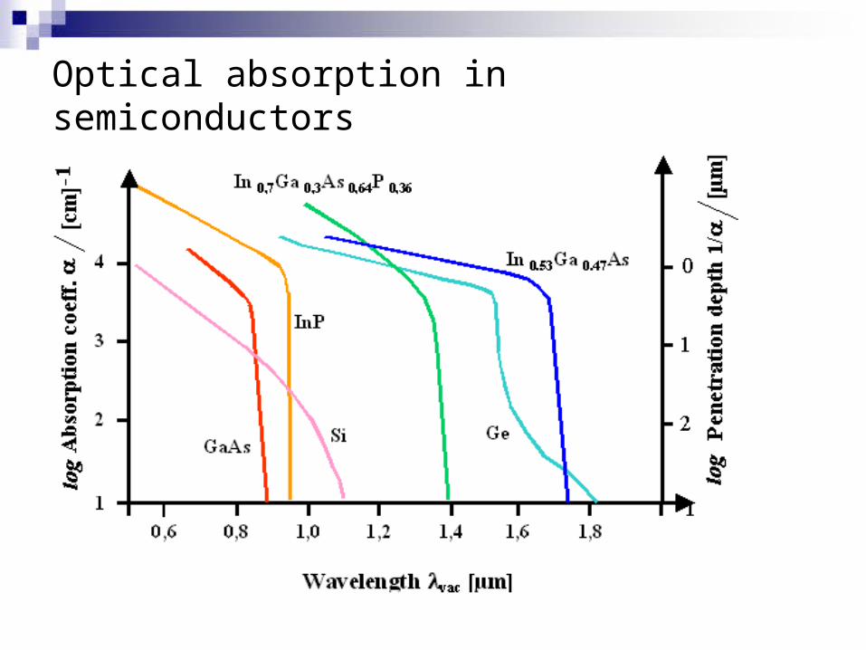
Optical absorption in semiconductors
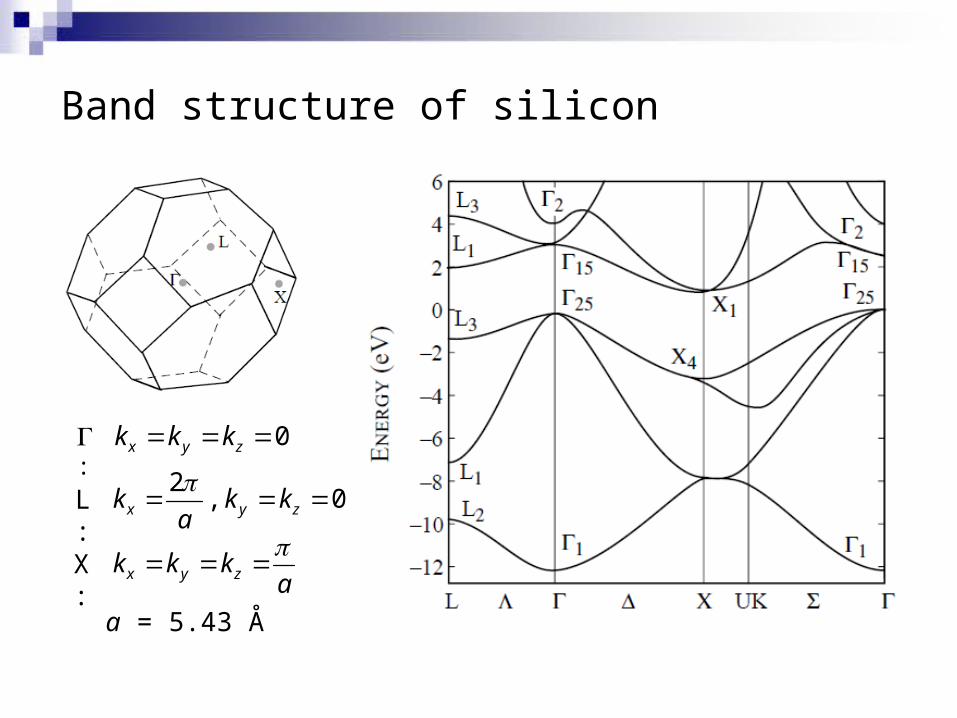
Band structure of silicon
0x y zk k k
2, 0x y zk k k
a
x y zk k ka
G:
L :
X :
a = 5.43 Å
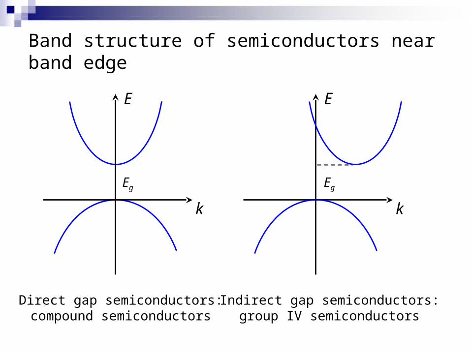
Band structure of semiconductors near band edge
k
E
k
E
Direct gap semiconductors:compound semiconductors
Indirect gap semiconductors:group IV semiconductors
Eg Eg
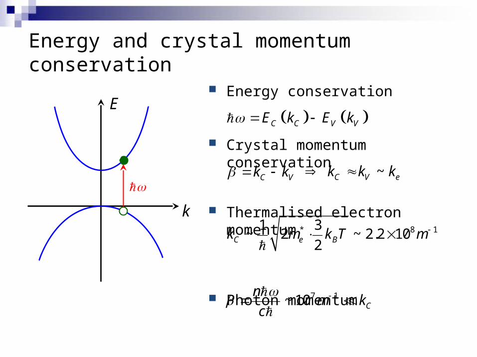
Energy and crystal momentum conservation
k
E Energy conservation
Crystal momentum conservation
Thermalised electron momentum
Photon momentum
C C V VE k E k
C Vk k
* 8 11 3~ 2 ~ 2.2 10
2C e Bk m k T m
7 1~ 10 C
nm k
c
~C V e k k k
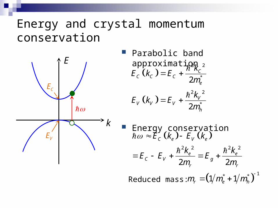
Energy and crystal momentum conservation
k
E Parabolic band approximation
Energy conservation
2 2 2 2
2 2
C e V e
e eC V g
r r
E k E k
k kE E E
m m
2 2
*2C
C C Ce
kE k E
m
2 2
*2V
V V Vh
kE k E
m
EC
EV
1* *1 1r e hm m m
Reduced mass:
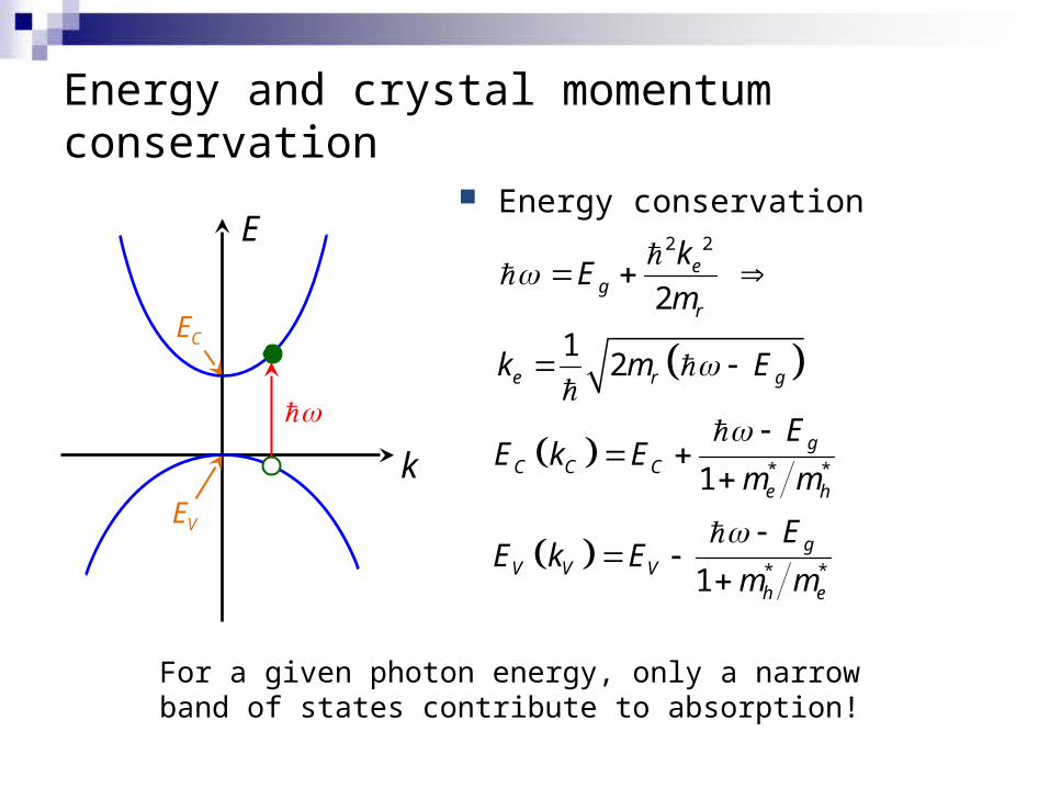
Energy and crystal momentum conservation
k
E
Energy conservation2 2
2e
gr
kE
m
EC
EV
12e r gk m E
* *1g
C C Ce h
EE k E
m m
* *1g
V V Vh e
EE k E
m m
For a given photon energy, only a narrow band of states contribute to absorption!
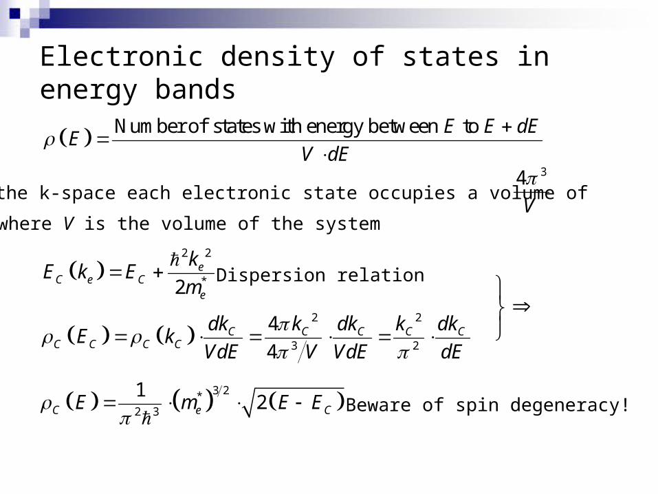
Electronic density of states in energy bands
Number of states with energy between to E E dEE
V dE
In the k-space each electronic state occupies a volume of34
V
where V is the volume of the system
2 2
3 2
4
4C C C C C
C C C C
dk k dk k dkE k
VdE V VdE dE
2 2
*2e
C e Ce
kE k E
m
Dispersion relation
3 2*2 3
12C e CE m E E
Beware of spin degeneracy!
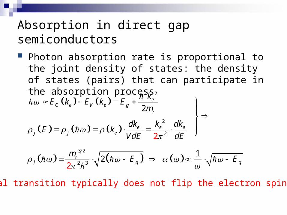
Absorption in direct gap semiconductors
Photon absorption rate is proportional to the joint density of states: the density of states (pairs) that can participate in the absorption process
2 2
2e
C e V e gr
kE k E k E
m
2
22e e e
j j e
dk k dkE k
VdE dE
3 2
2 32
12r
j g g
mE E
Optical transition typically does not flip the electron spin state
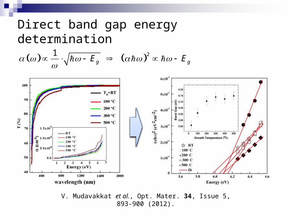
Direct band gap energy determination
21g gE E
V. Mudavakkat et al., Opt. Mater. 34, Issue 5, 893-900 (2012).
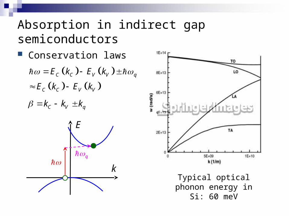
Conservation laws
Absorption in indirect gap semiconductors
k
E
q
C C V V q
C C V V
E k E k
E k E k
C V qk k k
Typical optical phonon energy in Si: 60 meV
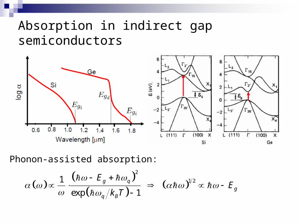
Absorption in indirect gap semiconductors
2
1 21
exp 1
g q
g
q B
E E
k T
Phonon-assisted absorption:
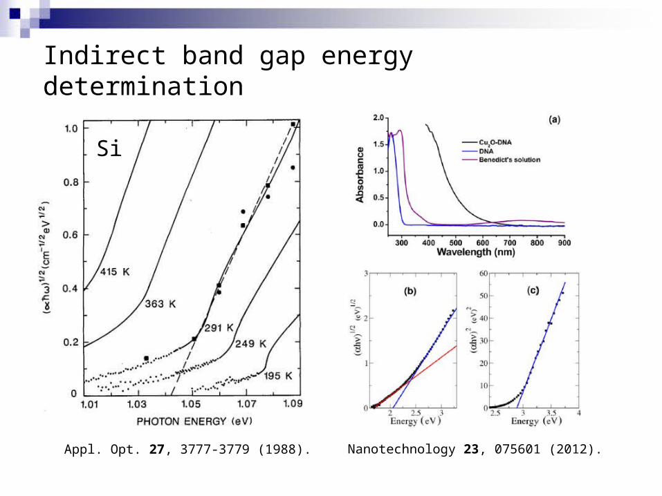
Indirect band gap energy determination
Appl. Opt. 27, 3777-3779 (1988).
Si
Nanotechnology 23, 075601 (2012).
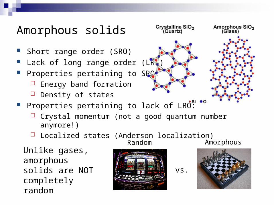
Amorphous solids
Short range order (SRO) Lack of long range order (LRO) Properties pertaining to SRO:
Energy band formation Density of states
Properties pertaining to lack of LRO: Crystal momentum (not a good quantum number anymore!) Localized states (Anderson localization)
Unlike gases, amorphous solids are NOT completely random
AmorphousRandom
vs.
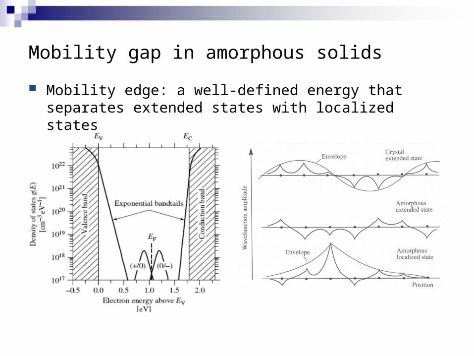
Mobility gap in amorphous solids
Mobility edge: a well-defined energy that separates extended states with localized states
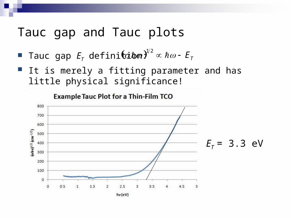
Tauc gap and Tauc plots
Tauc gap ET definition:
It is merely a fitting parameter and has little physical significance!
1 2
TE
ET = 3.3 eV
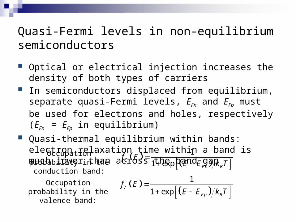
Quasi-Fermi levels in non-equilibrium semiconductors
Optical or electrical injection increases the density of both types of carriers
In semiconductors displaced from equilibrium, separate quasi-Fermi levels, EFn and EFp must be used for electrons and holes, respectively (EFn = EFp in equilibrium)
Quasi-thermal equilibrium within bands: electron relaxation time within a band is much lower than across the band gap
1
1 expV
Fp B
f EE E k T
1
1 expC
Fn B
f EE E k T
Occupation probability in the conduction band:
Occupation probability in the valence band:
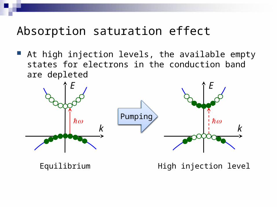
Absorption saturation effect
At high injection levels, the available empty states for electrons in the conduction band are depleted
Equilibrium High injection level
k
E
k
E
Pumping
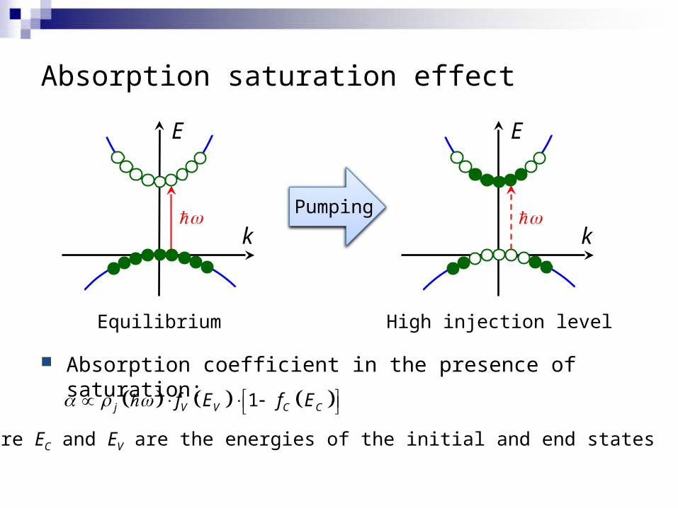
Absorption saturation effect
Absorption coefficient in the presence of saturation:
Equilibrium High injection level
1j V V C Cf E f E
k
E
k
E
Pumping
Here EC and EV are the energies of the initial and end states
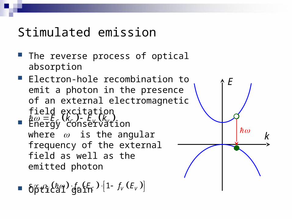
Stimulated emission
The reverse process of optical absorption Electron-hole recombination to emit a
photon in the presence of an external electromagnetic field excitation
Energy conservation
Optical gain
k
E
C C V VE k E k
1j C C V Vs f E f E
where w is the angular frequency of the external field as well as the emitted photon
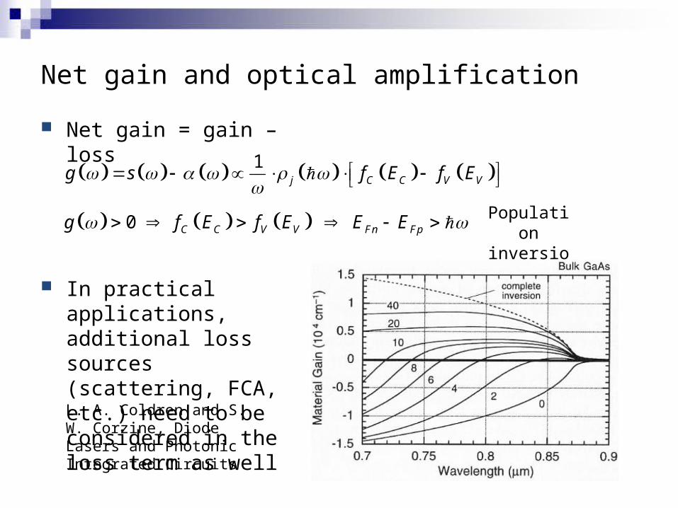
Net gain and optical amplification
Net gain = gain – loss
In practical applications, additional loss sources (scattering, FCA, etc.) need to be considered in the loss term as well
1j C C V Vg s f E f E
0 C C V V Fn Fpg f E f E E E Population inversion
L. A. Coldren and S. W. Corzine, Diode Lasers and Photonic Integrated Circuits
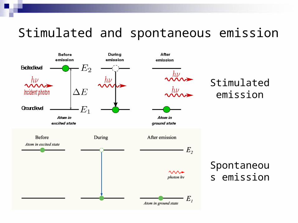
Stimulated and spontaneous emission
Stimulated emission
Spontaneous emission
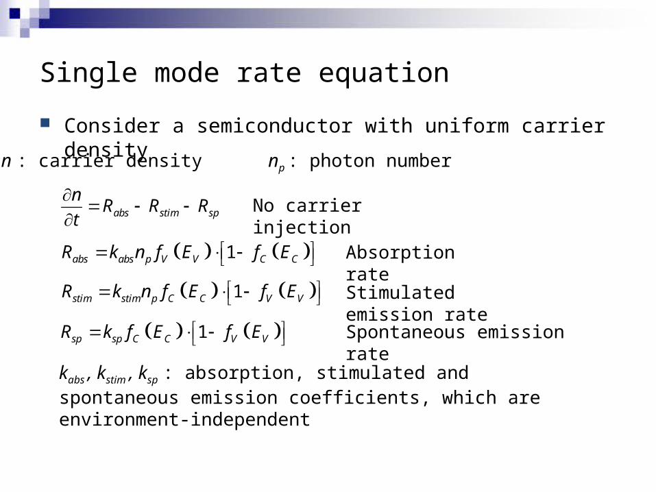
Single mode rate equation
Consider a semiconductor with uniform carrier density
n : carrier density np : photon number
abs stim sp
nR R R
t
1abs abs p V V C CR k n f E f E
1stim stim p C C V VR k n f E f E
1sp sp C C V VR k f E f E
kabs , kstim , ksp : absorption, stimulated and spontaneous emission coefficients, which are environment-independent
Absorption rate
Stimulated emission rate
Spontaneous emission rate
No carrier injection
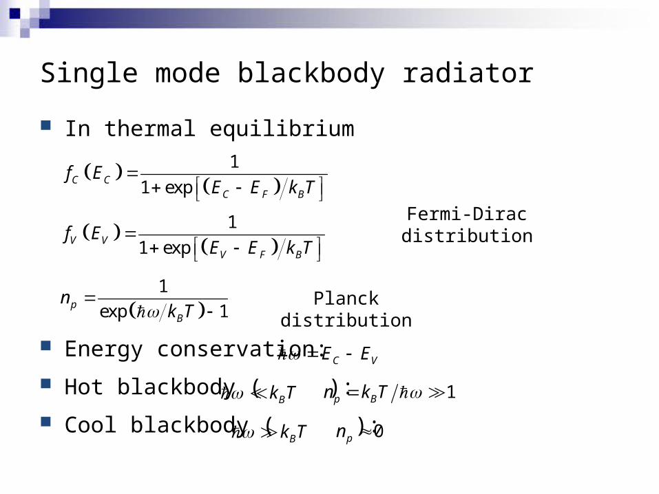
Single mode blackbody radiator
In thermal equilibrium
Energy conservation:
Hot blackbody ( ):
Cool blackbody ( ):
1
1 expC C
C F B
f EE E k T
1
1 expV V
V F B
f EE E k T
1
exp 1pB
nk T
Fermi-Dirac distribution
Planck distribution
Bk T 1p Bn k T
Bk T 0pn
C VE E
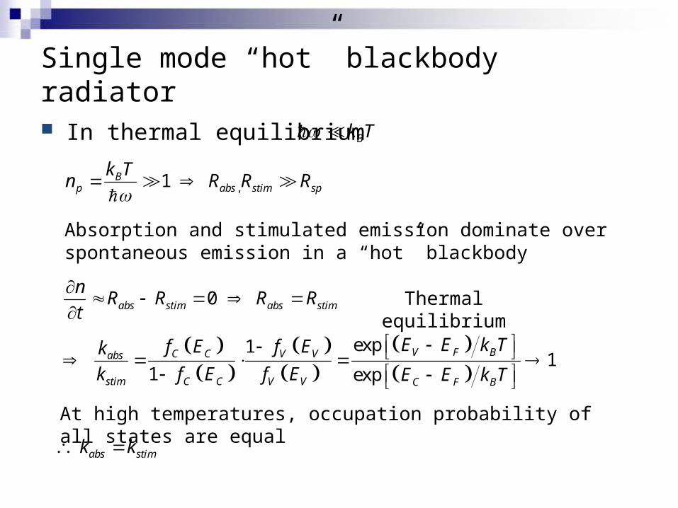
Single mode “hot” blackbody radiator
In thermal equilibrium Bk T
,1Bp abs stim sp
k Tn R R R
0abs stim abs stim
nR R R R
t
exp11
1 expV F BC C V Vabs
stim C C V V C F B
E E k Tf E f Ek
k f E f E E E k T
Thermal equilibrium
abs stim k k
Absorption and stimulated emission dominate over spontaneous emission in a “hot” blackbody
At high temperatures, occupation probability of all states are equal
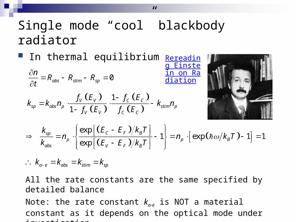
Single mode “cool” blackbody radiator
In thermal equilibrium
0abs stim sp
nR R R
t
1
1V V C C
sp abs p stim pV V C C
f E f Ek k n k n
f E f E
exp1 exp 1 1
expC F Bsp
p p Babs V F B
E E k Tk n n k T
k E E k T
a e abs stim sp k k k k
All the rate constants are the same specified by detailed balance
Note: the rate constant ka-e is NOT a material constant as it depends on the optical mode under investigation
Rereading Einstein on Radiation
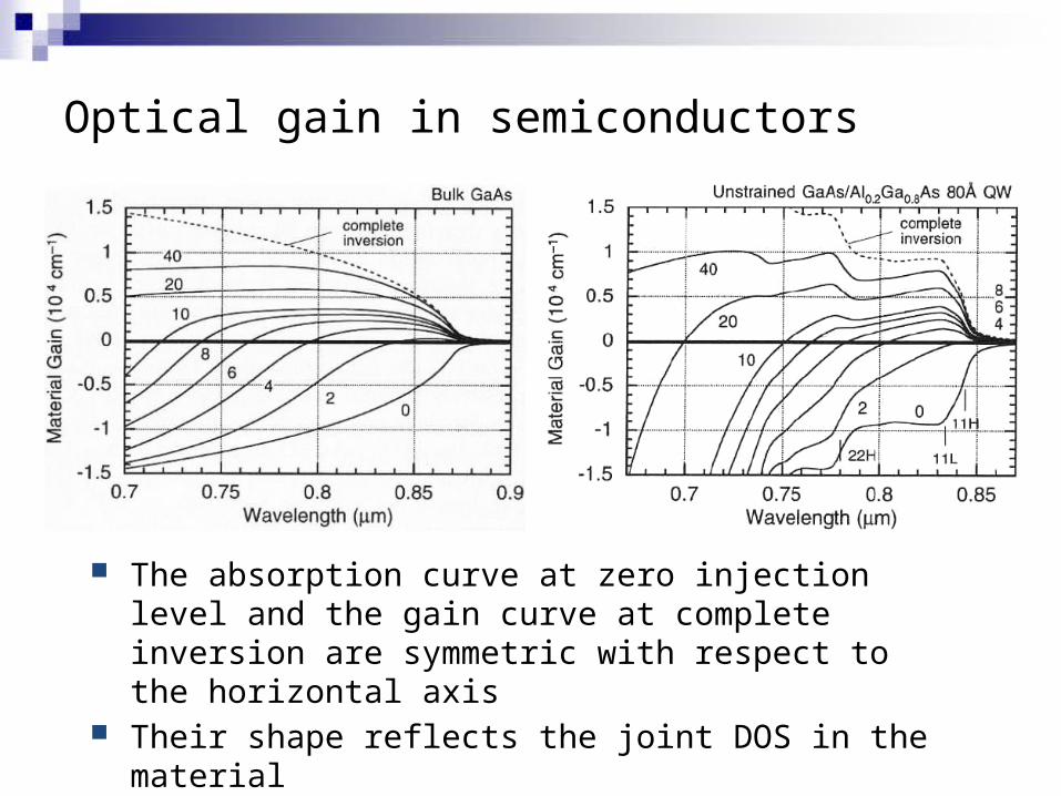
Optical gain in semiconductors
The absorption curve at zero injection level and the gain curve at complete inversion are symmetric with respect to the horizontal axis
Their shape reflects the joint DOS in the material
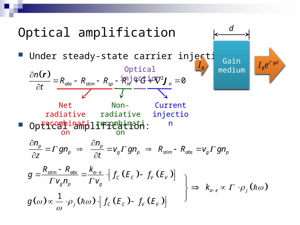
Optical amplification
Under steady-state carrier injection:
Optical amplification:
2 0abs stim sp nr n
nR R R R G
t
r
J
Gain medium
Net radiative recombination
Non-radiative recombination
Current injection
0I 0gdI e
d
stim abs a eC C V V
g p g
R R kg f E f E
v n v
1j C C V Vg f E f E
p pp g p stim abs g p
n ngn v gn R R v gn
z t
a e jk
Optical injection
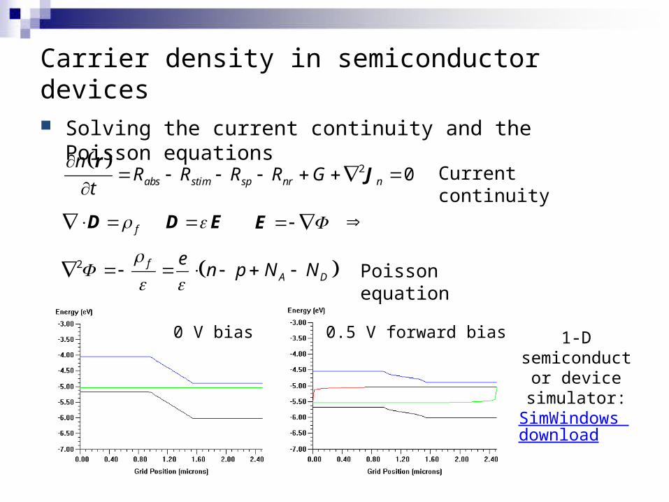
Carrier density in semiconductor devices
Solving the current continuity and the Poisson equations
2 0abs stim sp nr n
nR R R R G
t
r
J Current continuity
f D D E E
2 fA D
en p N N
Poisson equation
0 V bias 0.5 V forward bias 1-D semiconductor
device simulator:
SimWindows download
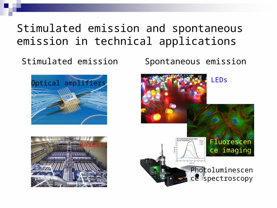
Stimulated emission and spontaneous emission in technical applications
Stimulated emission Spontaneous emission
Optical amplifiers
Lasers
LEDs
Fluorescence imaging
Photoluminescence spectroscopy
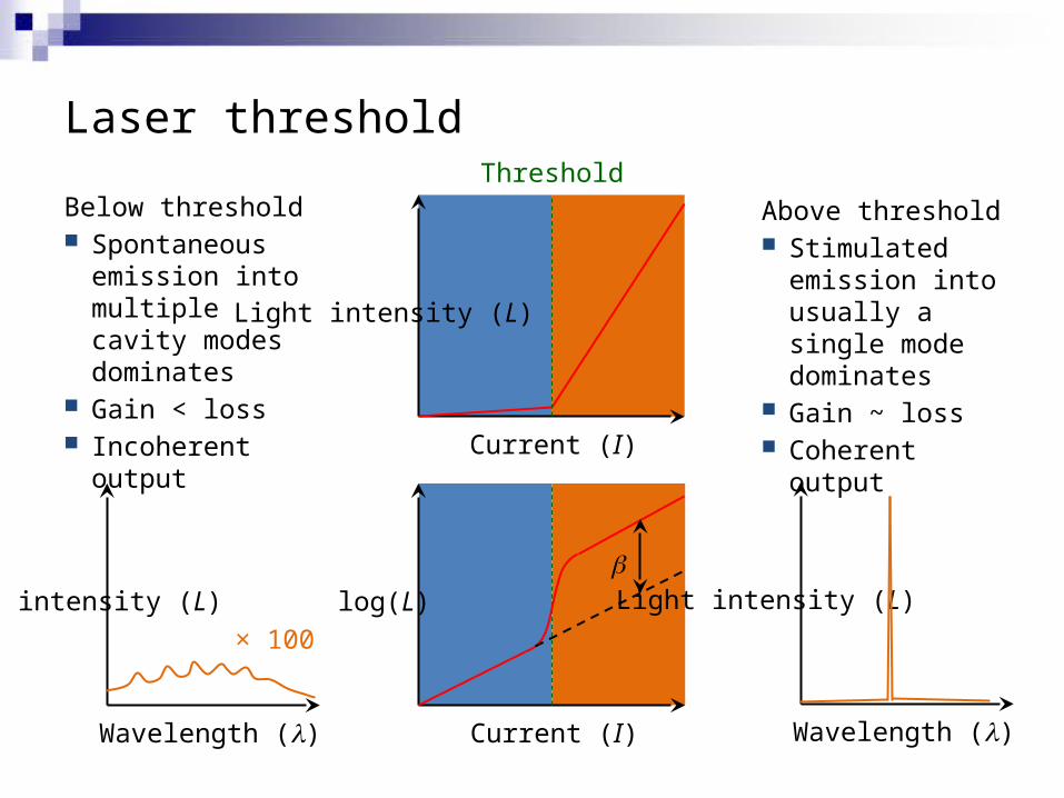
Laser threshold
Ligh
t in
tens
ity (
L)
Current (I)
ThresholdBelow threshold Spontaneous
emission into multiple cavity modes dominates
Gain < loss Incoherent output
Above threshold Stimulated
emission into usually a single mode dominates
Gain ~ loss Coherent output
log(
L)
Current (I)
b
Ligh
t in
tens
ity (
L)
Wavelength (l)Li
ght
inte
nsity
(L)
Wavelength (l)
× 100
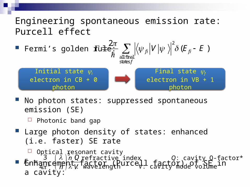
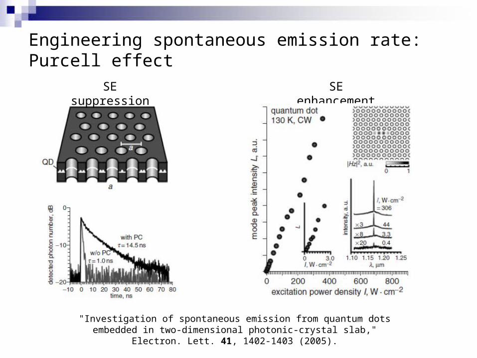
Engineering spontaneous emission rate: Purcell effect
Fermi’s golden rule:
No photon states: suppressed spontaneous emission (SE) Photonic band gap
Large photon density of states: enhanced (i.e. faster) SE rate Optical resonant cavity
Enhancement factor (Purcell factor) of SE in a cavity:
2
all finalstates
2( )f i f i
f
V E E
Initial state yi
electron in CB + 0 photonFinal state yf
electron in VB + 1 photon
3
2
3
4P
QF
n V
n : refractive index Q: cavity Q-factor*l : wavelength V: cavity mode volume
Engineering spontaneous emission rate: Purcell effect
SE suppression SE enhancement
"Investigation of spontaneous emission from quantum dots embedded in two-dimensional photonic-crystal slab," Electron. Lett. 41, 1402-1403 (2005).