muri annual review - ireap - the institute for...
TRANSCRIPT

Schottky Diode and MOSFET RF-Detector and Focused Ion Beam Post-Processing
MURI Annual Review
Woochul Jeon, Robert Newcomb Todd Firestone, John Rodgers
& John MelngailisUniversity of Maryland.

Original Project Objectives:
- Direct analog microwave level measurement on a chip(goal: up to 100GHz) using
a) Schottky diodesb) Thermal detectors
- Incorporation of RF detectors on chips, including FIB diode fabrication on existing chips
- Focused ion beam diagnosis circuit restructuring and device diagnosis by burned out element sectioning
Changes to Objectives:- Thermal detectors not pursued- Concentrate on lower frequency <10GHz- MOSFET power detectors included

Outline
• Operation of Schottky power detector• Fabricated Schottky diodes by CMOS process• Fabricated Schottky diodes by FIB as a post
CMOS process• MOSFET power detector• Effect on adding power detector to a logic circuit • Conclusion and future work

RF+
-DC
Operation of RF Power Detector
50pF 1kΩ
100ns
1.5V
0V
-1.5V
250mV
-20mV
RF input
Output
0s 100ns 200ns 300ns 400ns

Design a diode structure to minimize series resistance of n layer without using Silicon Molecular BeamEpitaxy(Si-MBE)
Minimize contact spacing
Schottky diode Design for CMOS process
n+2um
n - Substrate
Al AlSiO2
Schottky Contact Ohmic Contact

N+ doped area
Al
SiO2
FIB milling (2µm x 3 µm)
FIB Pt deposition
2µm scale 20µm scale
Fabrication of Schottky diode by FIB

RF direct injection test measurement setup
RF sourceAgilent 83731B
TektronicsTDS 620BOscilloscope
Cblock
Schottky diode Power detector
Cascade GSG probe150µm pitch

DC output vs. Pow er level
0
0.5
1
1.5
2
2.5
0 5 10 15 20
Pow er [dBm ]
Vout
[V]
5 GHZ 6 GHZ10GHz FIB 8GHz FIB
Frequency sweep
0.1
1
10
1 2 3 4 5 6 7 8 9 10Frequency(GHz)
Vou
t(V)
FIB CMOS compatilbe diode
Vout vs. Frequency sweep Vout vs. RF power sweep
RF direct injection test of evaporated contact diode and FIB diode made at UMd
(2µm x 3 µm contact area,)

• Schottky contact could not be made on CMOS process, though it depends on CMOS run itself.
• We have tried 4 times with different CMOS process. However, no Schottky contact was made.
Post CMOS process required
Photo of diode structure with test pads for Cascade probe made by MOSIS CMOS process
Schottky contactContact area: 2x2 µm2 - 40x 40 µm2
Ohmic contact
diode
100 µm
150 µm

Cross section a CMOS chip
Ion beam(milling)
e-beam (imaging)
M1M2M3
Pad
Via1µm
0.7µm
SiSiO2
6.8µm
52°

Fabricating Schottky diodes on CMOS chip by FIB
n substraten+
SiO2 Al
n
Al
FIB milling
n
Al
FIB Metal(Pt) deposition
Schottky contact
Mill SiO2 to expose metal layer for contacting to pad
To pad for directly injecting RF signal
Start with a CMOS chip
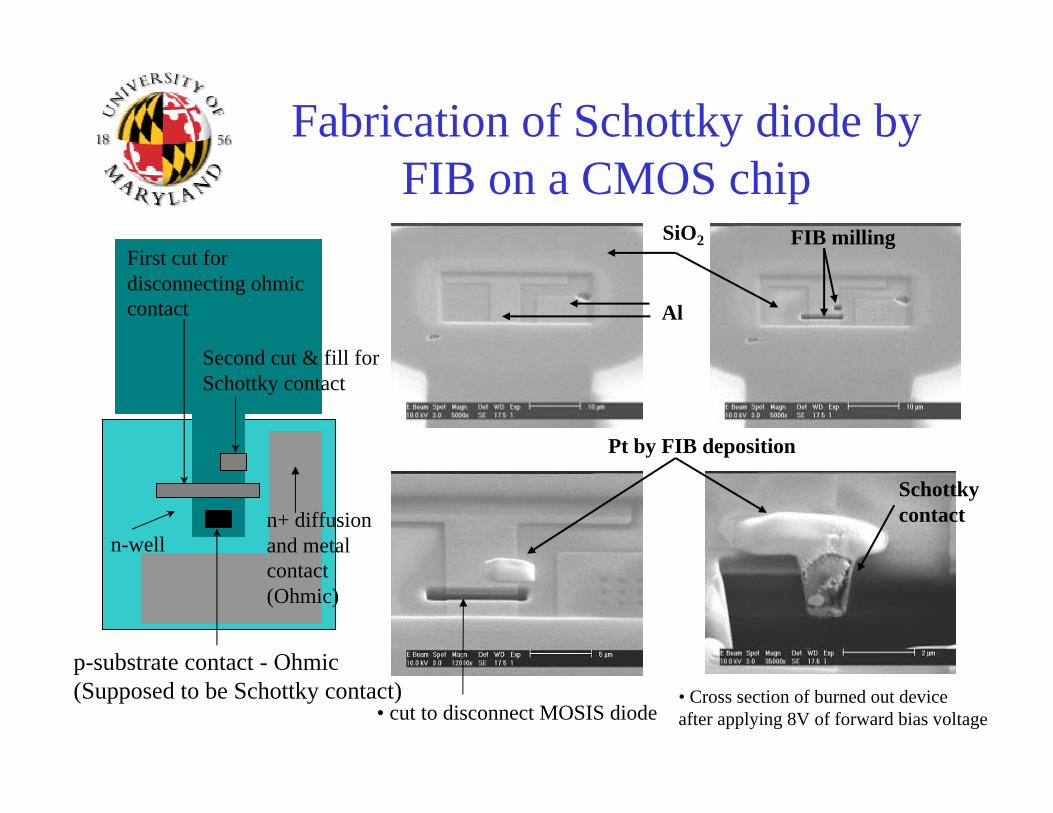
Fabrication of Schottky diode by FIB on a CMOS chip
SiO2
Al
FIB milling
Pt by FIB deposition
Schottky contact
• Cross section of burned out device after applying 8V of forward bias voltage• cut to disconnect MOSIS diode
p-substrate contact - Ohmic(Supposed to be Schottky contact)
First cut for disconnecting ohmiccontact
Second cut & fill for Schottky contact
n+ diffusion and metal contact(Ohmic)
n-well

FIB diode IV curve(log scale)
1.0E-09
1.0E-07
1.0E-05
1.0E-03
1.0E-01
1.0E+01
-10 -5 0 5
Vin(V)
Iout
(A)
FIB diode IV curve(-1V to 1V)
-3
0
3
6
9
12
15
18
21
24
-0.8 -0.4 0.0 0.4 0.8
Vin(V)
Iout
(uA
)
Measured result(DC)

Measured result (Power sweep)
0
0.5
1
1.5
2
2.5
-20 0 20
Pow er level(dBm )
Vout
(V)
1GHz
3GHz
5GHz
0
0.05
0.1
0.15
0.2
0.25
0 10 20
Pow er level(dBm )
0
0.2
0.4
0.6
0.8
1
1.2
1.4
1.6
0 10 20
Pow er level(dBm )
Power sweep at 1GHz, 3GHz, and 5GHz for three diodes: n-type 15µm2
diode, 6µm2 diode, and p-type 4µm2 Schottky diode, respectively

Frequency sw eep(1 to 15GHz) at 15dBm
0.01
0.1
1
10
1 3 5 7 9 11 13 15
Frequency(GHz)
Vout(V)
Measured result (Frequency sweep)
Frequency sweep from 1GHz to 15GHz at 15dBm
n-type 15µm2
n-type 8µm2
p-type 4µm2

Alternative CMOS design(MOSFET diode)
MOSFET diode power detector circuit, Pspice simulation result, and layout
150kΩ ,1k Ω5pF
RF pulse
M1
M2 M3
M4
Vbias
Bias circuit
M5Vout
100mV
-100mV
330mV
310mV
2GHz, 0.1Vpp, 3µs pulse width
12.5mV
8us 10us 12us 14us
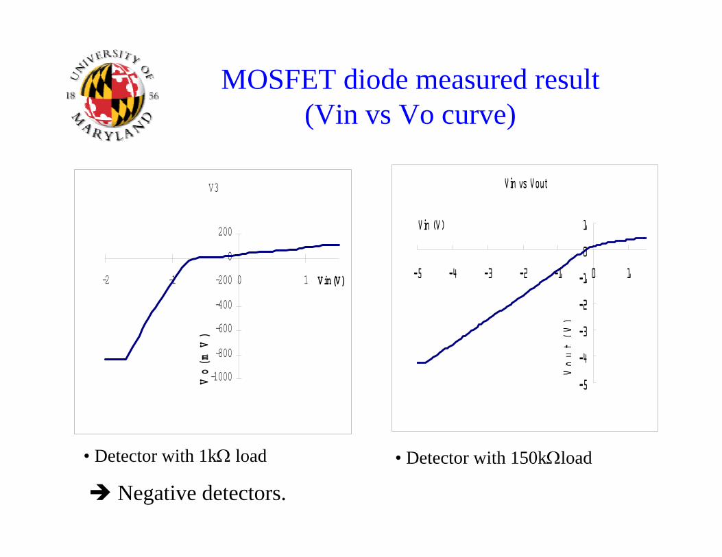
MOSFET diode measured result(Vin vs Vo curve)
Vin vs Vout
-5
-4
-3
-2
-1
0
1
-5 -4 -3 -2 -1 0 1
Vin (V)
Vout
(V)
Negative detectors.
• Detector with 1kΩ load • Detector with 150kΩload
V3
-1000-800-600-400-200
0200
-2 -1 0 1 V in(V )
Vo
(mV
)

RF direct injection test measurement setup
RF sourceAgilent 83731B
TektronicsTDS 620BOscilloscope
Cblock
MOSFET Power detector
DC bias
Cascade GSG probe150µm pitch

Frequency sweep
1.0E-03
1.0E-02
1.0E-01
1.0E+00
1.0E+01
1 3 5 7 9 11 13 15Frequency(GHz)
Vou
t(V)
0
0.2
0.4
0.6
-20 -15 -10 -5 0 5 10 15
Vo
ut
(V)
• Power sweep from –20dBm to 15dBm at 1GHz, 3GHz, and 5GHz
• Frequency sweep from 1GHz to 15GHz
• Pulse response time was 56 to 104nsec (1kΩ load) and 200 to 700nsec (150kΩ load) to –5 to 5dBm at 1 to 5GHz pulse
MOSFET detector measured result(RF direct injection with 1kΩ & 150kΩ load)
1GHz3GHz
5GHz
5dBm (150kΩ)
0dBm (150kΩ)10dBm (1kΩ)
5dBm (1kΩ)
0dBm (1kΩ)
150 k Ω
1 k Ω
Power sweep Frequency sweep
Vou
t(V)
dBm

Frequency sweep
0.01
0.1
1
10
1 3 5 7 9Frequency
Vout(V)
Power sweep (0dBm to 15dBm )
0
0.5
1
1.5
2
2.5
-15 -10 -5 0 5 10 15Power level(dBm )
Vo
ut(
V)
RF direct injection test for pn Junction diode(black line) and diode connected MOSFET(red line)*Green line: FIB Schottky diode power detector*Blue line: MOSFET power detector circuit for comparison
Better frequency response and sensitivity
Comparison of FIB diodes, pn junction diode & MOSFET detector with & without bias
MOSFET PD ckt.
Junction diode
MOSFET
Junction Diode at 10dBm
MOSFET at 10dBm
MOSFET PD ckt(150kΩ) at 5dBm
FIB Schottky diode(big)
FIB Schottky diode(Big) at 15 dBm
FIB Schottky diode(small) at 15 dBm
MOSFET PD (1kΩ) at 10dBm
Frequency sweep
Frequency (GHz)

Comparison table
Junction diode
MOSFETMOSFET detectorFIB diode
7dBm4dBm-12dBm-12dBm0dBm5dBm-10 dBmSensitivity(smallest possible detection)
> 10dBm> 10dBm25dBm15dBm> 15dBm> 15dBm> 25 dBmDynamic range
14.45.502.285.232.401.341.52Frequency response(Vout at 1GHz / Vout at 10GHz)
16µsec1.2µsec56nsec200nsec192nsec2.56µsec6µsecPulse response time
1kΩLoad
150kΩLoad
P-type 4µm2
N-type 6µm2
N-type 15µm2
Short pulse (< 1 µs) detection: MOSFET detector or small p-type FIB diode detector due to its fast pulse response time
Long pulse (>10 µs) detection: big n-type FIB diode is the best choice due to its flat frequency response, wide dynamic range, and good sensitivity

Effect on adding diode power detectors to a logic circuit
A
B
C
D
AB + CD logic circuit Series diode detector Parallel diode detector

Effect on adding diode power detectors to a logic circuit
Change output value when clock frequency becomes higher
With series diode With parallel diode Without detector
Low clock frequency (10MHz) High clock frequency (1GHz)
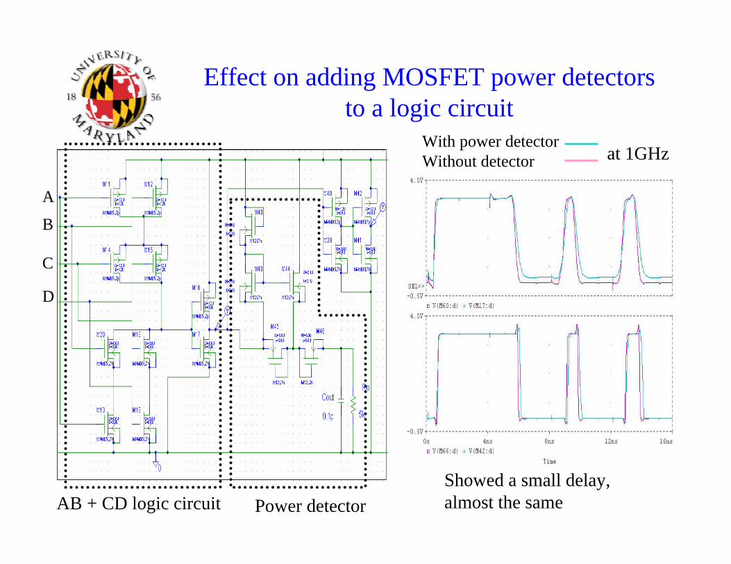
Effect on adding MOSFET power detectors to a logic circuit
A
B
C
D
AB + CD logic circuit Power detectorShowed a small delay, almost the same
With power detectorWithout detector at 1GHz

MOSFET detector circuit (Future work)Full-wave rectifier circuit
RF pulse
1kΩ5pF
M1 M2
Vi
Vo
M3 M4
M5 M6
0.3
0.4
0.5
0.6
0.7
0.8
0.9
1
1.1
-10 -5 0 5 10
Vi
Vo
Simulation result (Vi vs Vo, DC)

Detecting RF level on a PCB board
PCB board
IC 1 IC 2
IC 4
Input(RF pulse)
Output
Power detector
Power at node 1
Power detector
Power at node 2
Power detector
Power detector
Power detector
IC 3
IC 5
Power at node 3
Power at node 5
Power at node 4

Summary
• Schottky diodes were attempted by AMI 1.5µ, 0.5µ, and 0.35µ CMOS process through the MOSIS
• Schottky diodes were fabricated by FIB techniques on a CMOS chip and tested up to 15 GHz
• As an alternative CMOS design, MOSFET power detector circuit designed and tested
• pn junction diode and diode connected MOSFET detector tested and compared
• Schottky diode RF detector loading of logic circuit simulated

Publications:
Woochul Jeon, Todd M. Firestone John C. Rodgers, and John Melngailis,
“Design and fabrication os Schottky diode, on-chip RF detectors”
Solid State Electronics 48, 2089 (2004)
Woochul Jeon, Todd M. Firestone John C. Rodgers, and John Melngailis,“On-chip RF power detector using focused ion beam as a post-CMOS
fabrication process” to be published Electromagnetics Journal

Future work
- design (and implement) RF pulse detectors for system board,
- design (and implement) RF pulse detectors inside chips,
- build full wave rectifier circuits
- alter circuits with FIB
- test sensitivity of RFID tags to deprogramming with RF bursts (seeking industry funding)