nasa-dod lower process temperature lead-free … in accordance with ipc j- std-001es, space...
TRANSCRIPT
National Aeronautics and Space Administration (NASA)
NASA-DoD Lower Process Temperature Lead-Free Solder Project Overview
https://ntrs.nasa.gov/search.jsp?R=20140005435 2018-07-16T14:27:52+00:00Z
National Aeronautics and Space Administration (NASA)
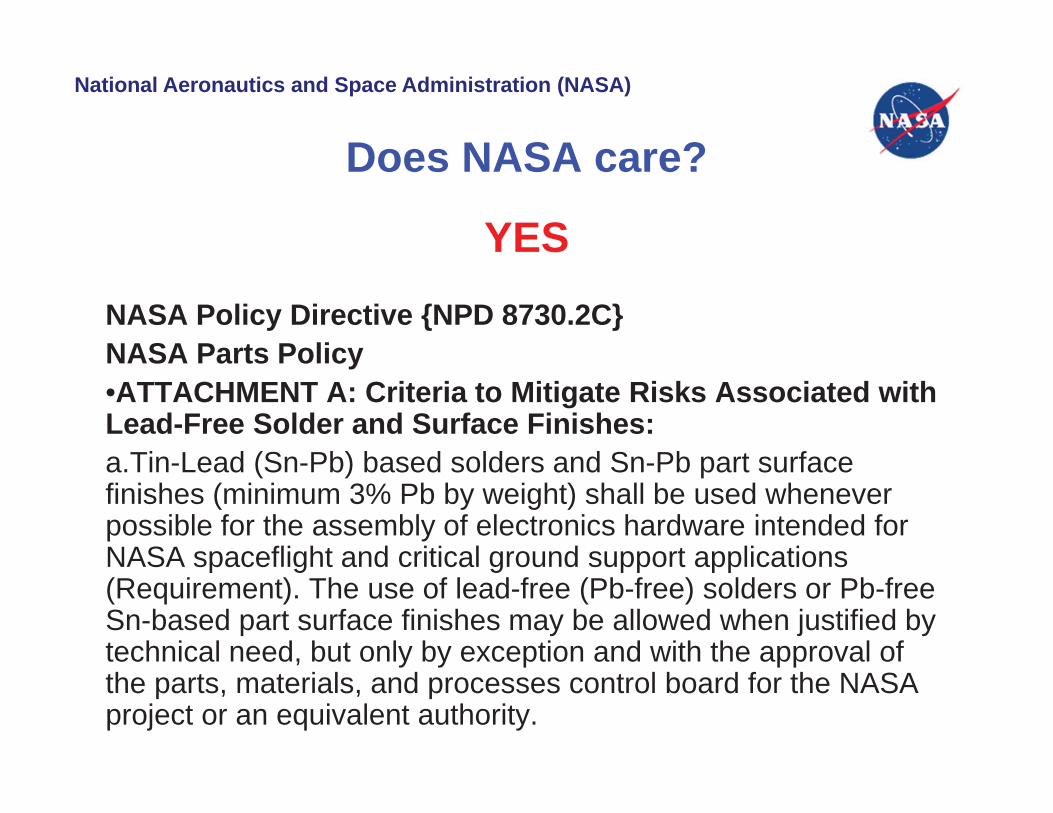
Does NASA care?
YES
NASA Policy Directive {NPD 8730.2C} NASA Parts Policy •ATTACHMENT A: Criteria to Mitigate Risks Associated with Lead-Free Solder and Surface Finishes: a.Tin-Lead (Sn-Pb) based solders and Sn-Pb part surface finishes (minimum 3% Pb by weight) shall be used whenever possible for the assembly of electronics hardware intended for NASA spaceflight and critical ground support applications (Requirement). The use of lead-free (Pb-free) solders or Pb-free Sn-based part surface finishes may be allowed when justified by technical need, but only by exception and with the approval of the parts, materials, and processes control board for the NASA project or an equivalent authority.
National Aeronautics and Space Administration (NASA)
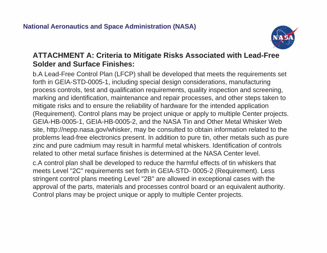
ATTACHMENT A: Criteria to Mitigate Risks Associated with Lead-Free Solder and Surface Finishes: b.A Lead-Free Control Plan (LFCP) shall be developed that meets the requirements set forth in GEIA-STD-0005-1, including special design considerations, manufacturing process controls, test and qualification requirements, quality inspection and screening, marking and identification, maintenance and repair processes, and other steps taken to mitigate risks and to ensure the reliability of hardware for the intended application (Requirement). Control plans may be project unique or apply to multiple Center projects. GEIA-HB-0005-1, GEIA-HB-0005-2, and the NASA Tin and Other Metal Whisker Web site, http://nepp.nasa.gov/whisker, may be consulted to obtain information related to the problems lead-free electronics present. In addition to pure tin, other metals such as pure zinc and pure cadmium may result in harmful metal whiskers. Identification of controls related to other metal surface finishes is determined at the NASA Center level. c.A control plan shall be developed to reduce the harmful effects of tin whiskers that meets Level "2C" requirements set forth in GEIA-STD- 0005-2 (Requirement). Less stringent control plans meeting Level "2B" are allowed in exceptional cases with the approval of the parts, materials and processes control board or an equivalent authority. Control plans may be project unique or apply to multiple Center projects.
National Aeronautics and Space Administration (NASA)
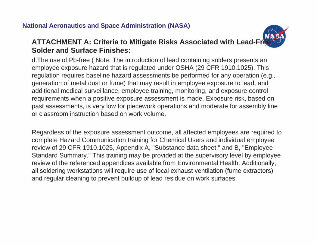
ATTACHMENT A: Criteria to Mitigate Risks Associated with Lead-Free Solder and Surface Finishes: d.The use of Pb-free ( Note: The introduction of lead containing solders presents an employee exposure hazard that is regulated under OSHA (29 CFR 1910.1025). This regulation requires baseline hazard assessments be performed for any operation (e.g., generation of metal dust or fume) that may result in employee exposure to lead, and additional medical surveillance, employee training, monitoring, and exposure control requirements when a positive exposure assessment is made. Exposure risk, based on past assessments, is very low for piecework operations and moderate for assembly line or classroom instruction based on work volume.
Regardless of the exposure assessment outcome, all affected employees are required to complete Hazard Communication training for Chemical Users and individual employee review of 29 CFR 1910.1025, Appendix A, "Substance data sheet," and B, "Employee Standard Summary." This training may be provided at the supervisory level by employee review of the referenced appendices available from Environmental Health. Additionally, all soldering workstations will require use of local exhaust ventilation (fume extractors) and regular cleaning to prevent buildup of lead residue on work surfaces.
National Aeronautics and Space Administration (NASA)
MSFC-STD-3012, Electrical, Electronic, and Electromechanical (EEE) Parts Management and
Control Requirements for MSFC Space Flight Hardware 5.3.2.1 Destructive Physical Analysis (DPA) • Requirements for DPA shall be as designated in Tables V, VI, or VII
for Grades 1, 2, and 3 EEE parts. DPA sample size shall be in accordance with MIL-STD-1580 unless otherwise specified herein. Any lot of parts not meeting the DPA acceptance criteria shall not be used in equipment without focal point EEE parts organization approval.
• In addition, all DPA samples from non QPL/QML/QPD manufactured EEE part lots shall be tested internally and externally for pure tin as defined in Section 5.4.4.1 herein.
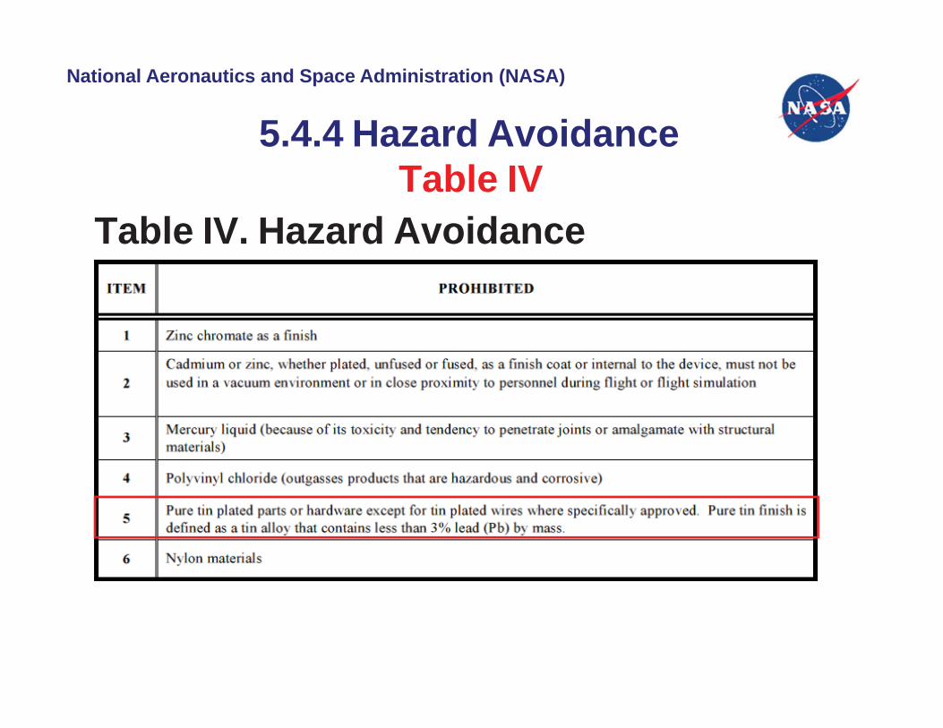
5.4.4 Hazard Avoidance • Grades 1, 2, and 3 EEE parts shall comply with the program
requirements for hazard avoidance (e.g. NSTS 1700.7, NASA-STD- 6016, or equivalent program document), Table IV, and the following subparagraphs. All EEE part grades, including Grade 4, shall avoid the prohibited materials listed in Table IV, Hazard Avoidance.
National Aeronautics and Space Administration (NASA)
5.4.4 Hazard Avoidance Table IV
Table IV. Hazard Avoidance
National Aeronautics and Space Administration (NASA)
5.4.4.1 Pure Tin Finish Avoidance
• Any EEE part where pure tin finish is not precluded by the military QPL/QML/QPD, or specification control document, shall be tested internally and externally for pure tin as defined in Table IV. The minimum sample size shall be two devices or two percent of the lot, whichever is greater, to a maximum of five samples. If parts fail to meet the 3% lead by mass requirement, the preferred method to mitigate the risk from pure tin is to solder dip the expose tin finish in accordance with GEIA-STD-0006, Requirements for Using Solder Dip to Replace the Finish on Electronic Piece Parts. If the solder dip process is not practical, the risk from pure tin shall be mitigated in accordance with IPC J- STD-001ES, Space Applications Electronic Hardware Addendum to IPC J-STD- 001E, Requirements for Soldered Electrical and Electronic Assemblies, Clause 0.1.6, Use of Lead-Free Tin.
National Aeronautics and Space Administration (NASA)
Table V. Standard Parts and Selection Preferences for Grade 1
• Note 6: The MIL-PRF-55681/1 style CDR02 ceramic chip capacitors shall not be used in Grade 1 applications. This particular chip has a large length to width ratio (0.18" x 0.05") which makes this chip highly susceptible to cracking as a result of board flexing.
• The use of MIL-PRF-55681 ceramic chip capacitors with Termination Style "W" or "Y“ is PROHIBITED. Termination style "Y" is pure tin and termination style "W" gives the manufacturer the option to use either pure tin or a tin-lead alloy as a termination finish.
• Note 19: 100% screening shall be performed per MIL-PRF- 3098 Table I Product Level S, including the following test inspections: PIND testing, radiographic Inspection, and Percent Defective Allowable (PDA) of 5%. Pure tin shall be prohibited as a final finish.
National Aeronautics and Space Administration (NASA)
NASA-DoD LEAD-FREE ELECTRONICS PROJECT:
Lower Process Temperature Pb-Free Solders
National Aeronautics and Space Administration (NASA)
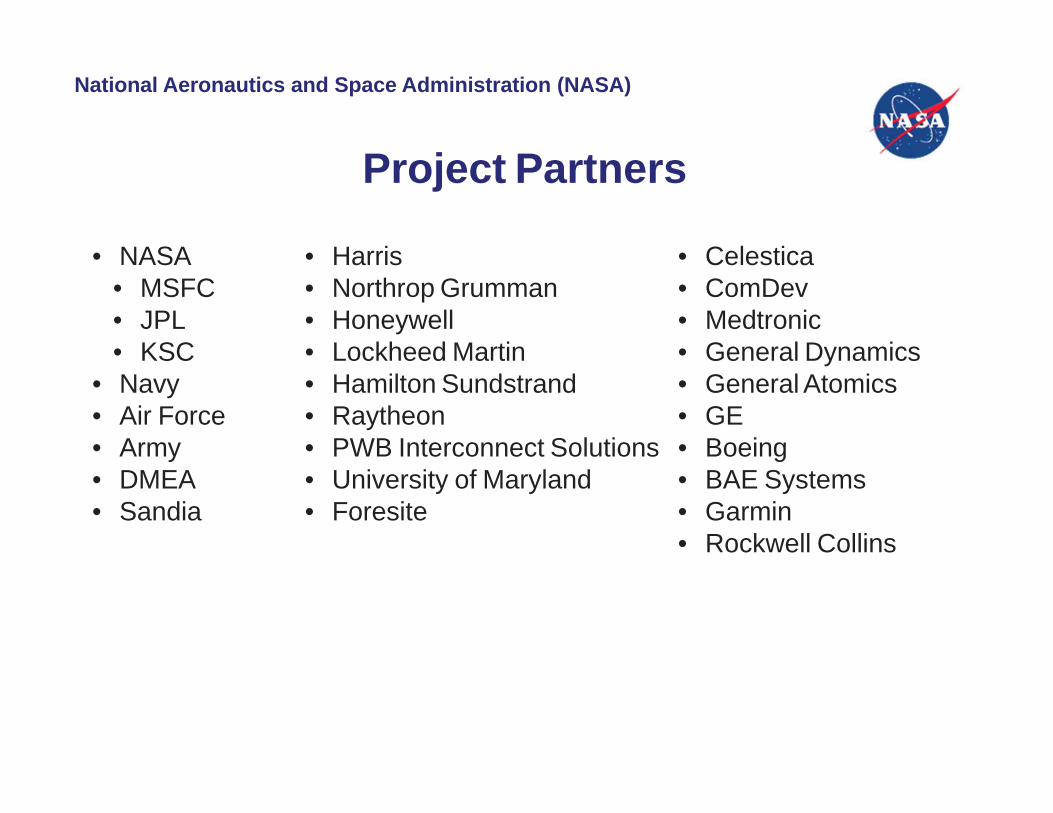
Project Partners
• NASA • MSFC • JPL • KSC
• Navy • Air Force • Army • DMEA • Sandia
• Harris • Northrop Grumman • Honeywell • Lockheed Martin • Hamilton Sundstrand • Raytheon • PWB Interconnect Solutions • University of Maryland • Foresite
• Celestica • ComDev • Medtronic • General Dynamics • General Atomics • GE • Boeing • BAE Systems • Garmin • Rockwell Collins

National Aeronautics and Space Administration (NASA)
Previous Efforts The NASA-DoD consortia group has lead the industry in the understanding of
lead-free bismuth containing solder alloys The JCAA/JGPP Phase I investigation effort, the consortia included the
NCMS lead-free bismuth containing solder alloy as their 1997 work had shown it had some promise as an alternative candidate solder alloy system for tin/lead solder.
The JCAA/JGPP Phase I investigation results {2006} demonstrated that the lead-free bismuth containing solder alloy had very good performance in harsh environmental testing but it also had some compatibility issues to be further characterized. • For many components SACB solder joints were at least as reliable as the SnPb controls during the
combined environments and thermal cycling tests. (Exceptions were when SACB was contaminated with SnPb)
• For SACB solder alloy, SnPb contamination usually has a detrimental effect on reliability. The degree of degradation of SACB solder joint reliability appears to be inversely proportional to the amount of SnPb contamination in the solder joint. Therefore, soldering with SACB solder requires appropriate factory management to eliminate lead contamination.
• Pb contamination must be better understood and controlled if SACB solder is to be utilized. The level of control of Pb contamination required when soldering with SACB may not be available to service centers and might pose an unacceptable risk to high-performance systems. If Pb contamination is not controllable, that may preclude the use of SACB solder on some or all aerospace and defense electronics.
National Aeronautics and Space Administration (NASA)
Previous Efforts
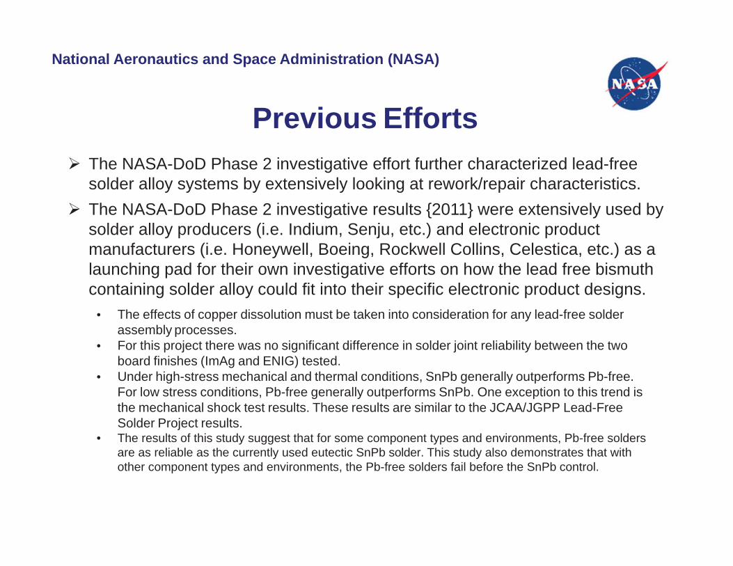
The NASA-DoD Phase 2 investigative effort further characterized lead-free solder alloy systems by extensively looking at rework/repair characteristics.
The NASA-DoD Phase 2 investigative results {2011} were extensively used by solder alloy producers (i.e. Indium, Senju, etc.) and electronic product manufacturers (i.e. Honeywell, Boeing, Rockwell Collins, Celestica, etc.) as a launching pad for their own investigative efforts on how the lead free bismuth containing solder alloy could fit into their specific electronic product designs.
• The effects of copper dissolution must be taken into consideration for any lead-free solder assembly processes.
• For this project there was no significant difference in solder joint reliability between the two board finishes (ImAg and ENIG) tested.
• Under high-stress mechanical and thermal conditions, SnPb generally outperforms Pb-free. For low stress conditions, Pb-free generally outperforms SnPb. One exception to this trend is the mechanical shock test results. These results are similar to the JCAA/JGPP Lead-Free Solder Project results.
• The results of this study suggest that for some component types and environments, Pb-free solders are as reliable as the currently used eutectic SnPb solder. This study also demonstrates that with other component types and environments, the Pb-free solders fail before the SnPb control.

National Aeronautics and Space Administration (NASA)
Need The NASA-DoD Lead-Free Electronics Project confirmed that
pad cratering is one of the dominant failure modes that occur in various board level reliability tests, especially under dynamic loading = harsh environments.
Pad Cratering is a latent defect that may occur during assembly, rework, and post assembly handling and testing.
Pad cratering cannot be identified during back-end-of-line in- circuit test (ICT) or functional circuit test (FCT) protocols and poses a high reliability risk under mechanical and thermo- mechanical loading.
National Aeronautics and Space Administration (NASA)
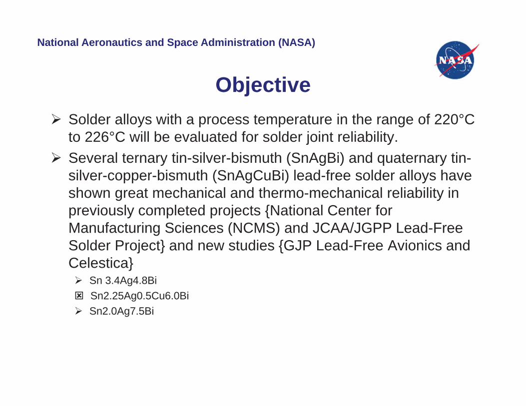
Objective Solder alloys with a process temperature in the range of 220°C
to 226°C will be evaluated for solder joint reliability. Several ternary tin-silver-bismuth (SnAgBi) and quaternary tin-
silver-copper-bismuth (SnAgCuBi) lead-free solder alloys have shown great mechanical and thermo-mechanical reliability in previously completed projects {National Center for Manufacturing Sciences (NCMS) and JCAA/JGPP Lead-Free Solder Project} and new studies {GJP Lead-Free Avionics and Celestica} Sn 3.4Ag4.8Bi Sn2.25Ag0.5Cu6.0Bi Sn2.0Ag7.5Bi
National Aeronautics and Space Administration (NASA)
Why this is Important
The proposed NASA-DoD Phase 3 investigation is fundamentally different than other industry activities because the consortia is proposing to conduct testing that is applicable to the entire electronics industry in an unbiased, open architecture format that will provide further understanding of bismuth containing solder alloy systems in relation to current tin/lead and SAC solder alloy soldering practices/procedures.
It is anticipated that the electronics industry will utilize the NASA-DoD Phase 3 investigation results as a springboard for further industry solder alloy investigative activities in a similar fashion to what occurred with the JCAA/JGPP and NASA-DoD Phase 2 investigation results.
National Aeronautics and Space Administration (NASA)
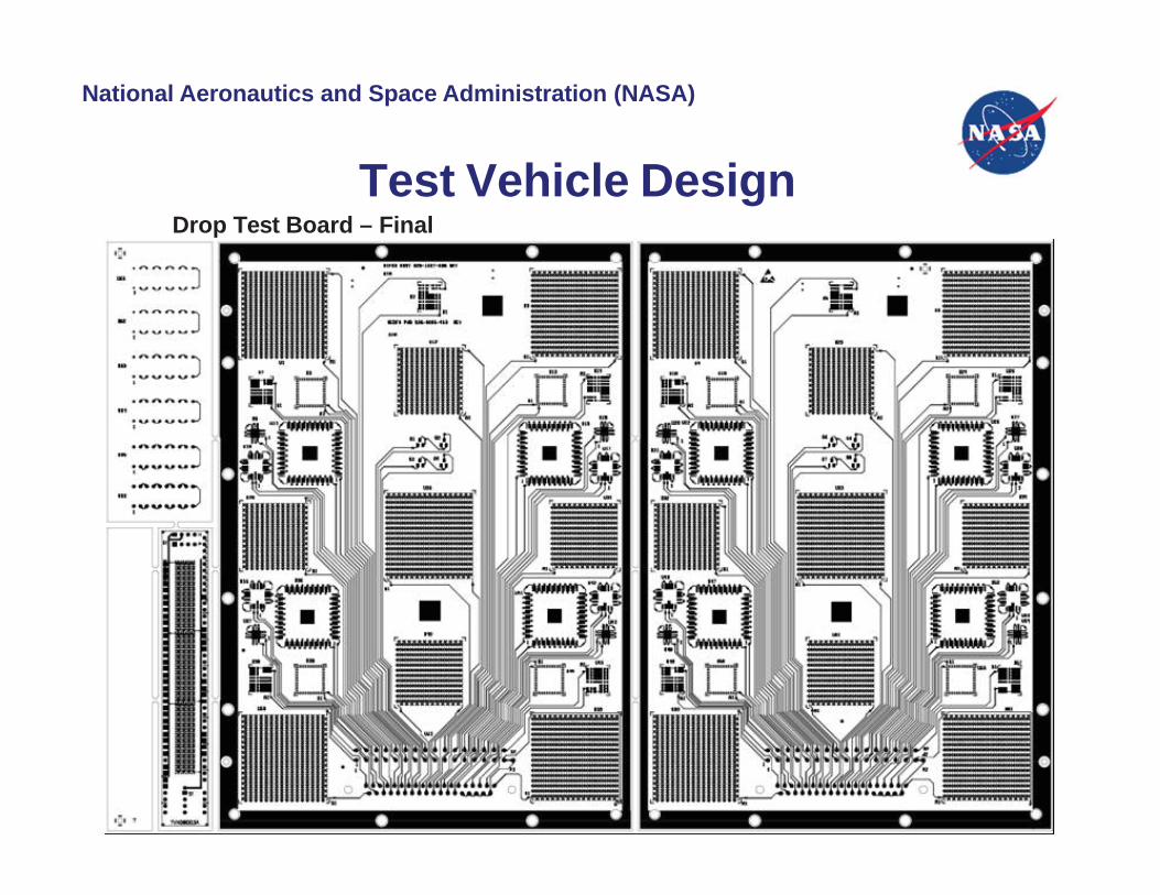
Test Vehicle Design
Drop Test Board – Final
National Aeronautics and Space Administration (NASA)
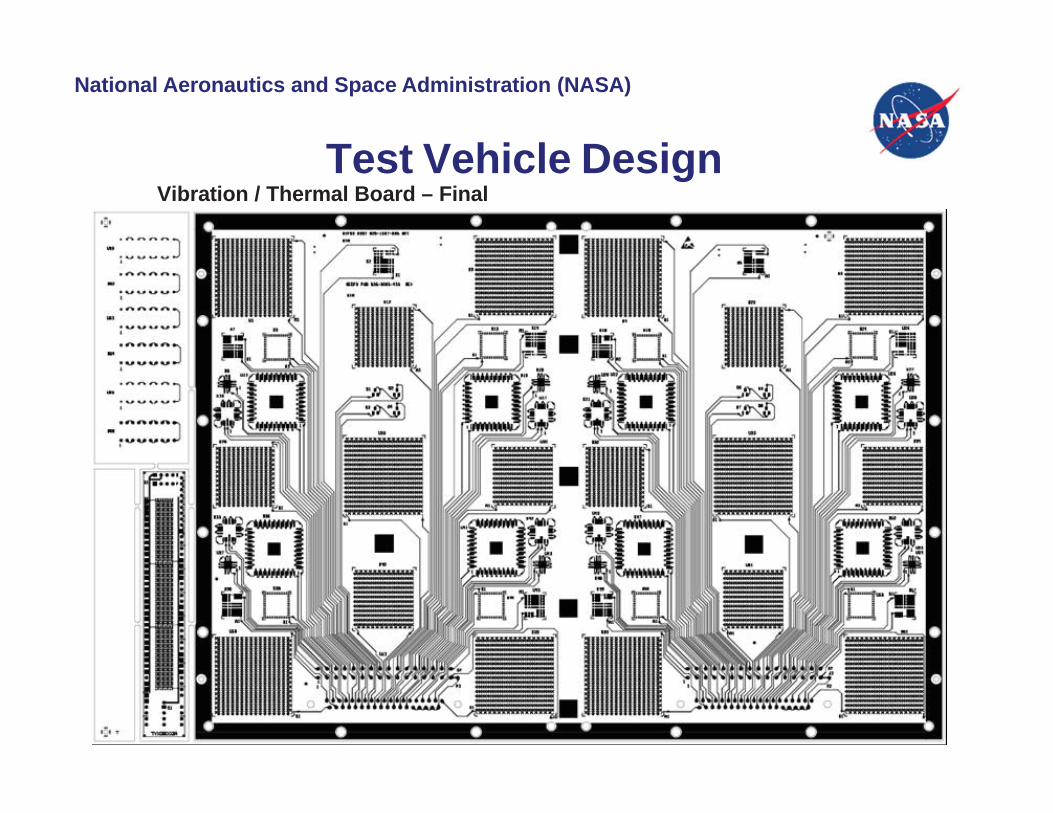
Test Vehicle Design Vibration / Thermal Board – Final
National Aeronautics and Space Administration (NASA)
Solder Alloy Selection • SnPb baseline 183oC • SAC305 baseline 217 – 219oC Lower process temperature LF solders • 91.8Sn 3.4Ag 4.8Bi {Indium Corporation}
• Melting Temperature 206 – 216oC • Commercial use; consumption volume unknown
• Sn2.25Ag0.5Cu6.0Bi {Indium Corporation} • Melting Temperature 205 – 215oC • Commercial use; consumption volume unknown
• Sn2.0Ag7.5Bi {Indium Corporation} • Melting Temperature 190 - 215oC • Commercial use; consumption volume unknown

National Aeronautics and Space Administration (NASA)
Materials Selection
Laminates Baseline – Isola 370HR Alternative - Isola 408HR
Board Finishes Primary board finish: Immersion silver (ImAg) Limited use: Electroless Nickel Immersion Gold (ENIG)
National Aeronautics and Space Administration (NASA)
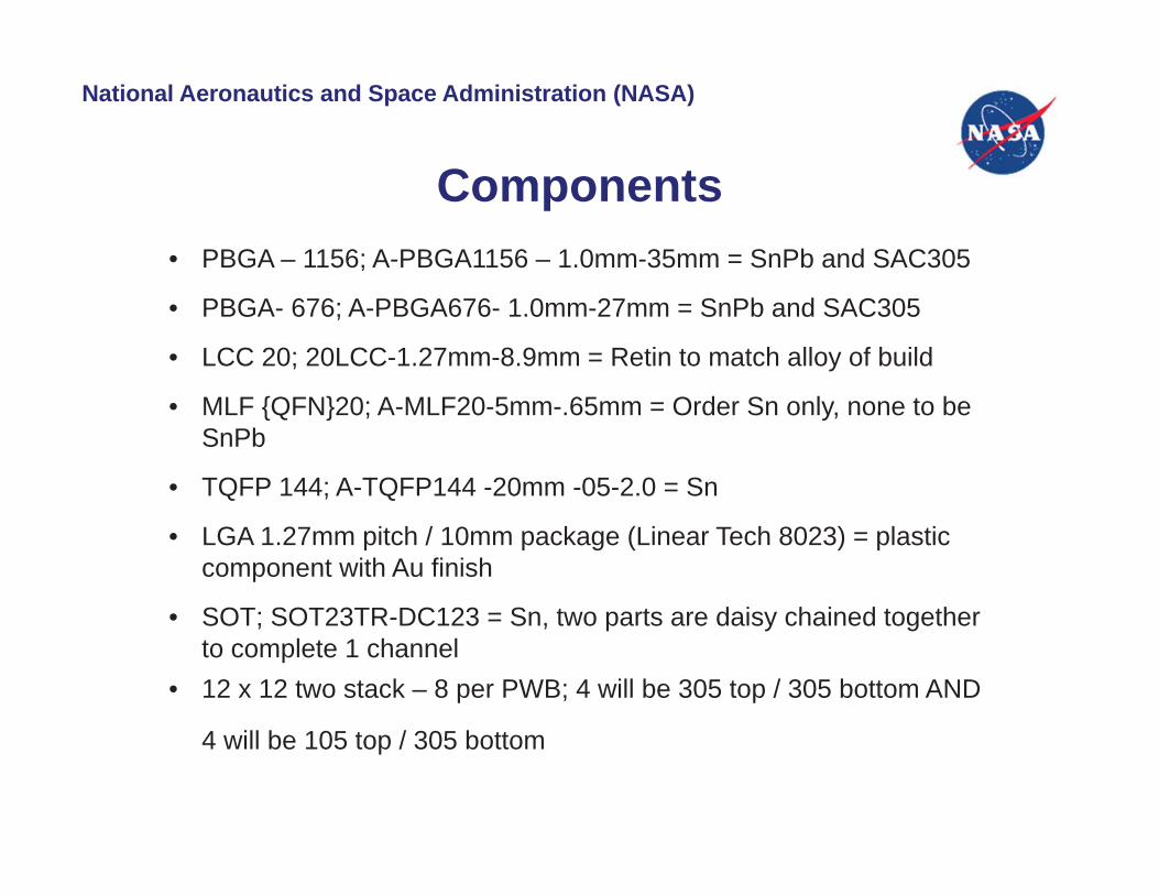
Components
• PBGA – 1156; A-PBGA1156 – 1.0mm-35mm = SnPb and SAC305
• PBGA- 676; A-PBGA676- 1.0mm-27mm = SnPb and SAC305
• LCC 20; 20LCC-1.27mm-8.9mm = Retin to match alloy of build
• MLF {QFN}20; A-MLF20-5mm-.65mm = Order Sn only, none to be SnPb
• TQFP 144; A-TQFP144 -20mm -05-2.0 = Sn
• LGA 1.27mm pitch / 10mm package (Linear Tech 8023) = plastic component with Au finish
• SOT; SOT23TR-DC123 = Sn, two parts are daisy chained together to complete 1 channel
• 12 x 12 two stack – 8 per PWB; 4 will be 305 top / 305 bottom AND
4 will be 105 top / 305 bottom
National Aeronautics and Space Administration (NASA)
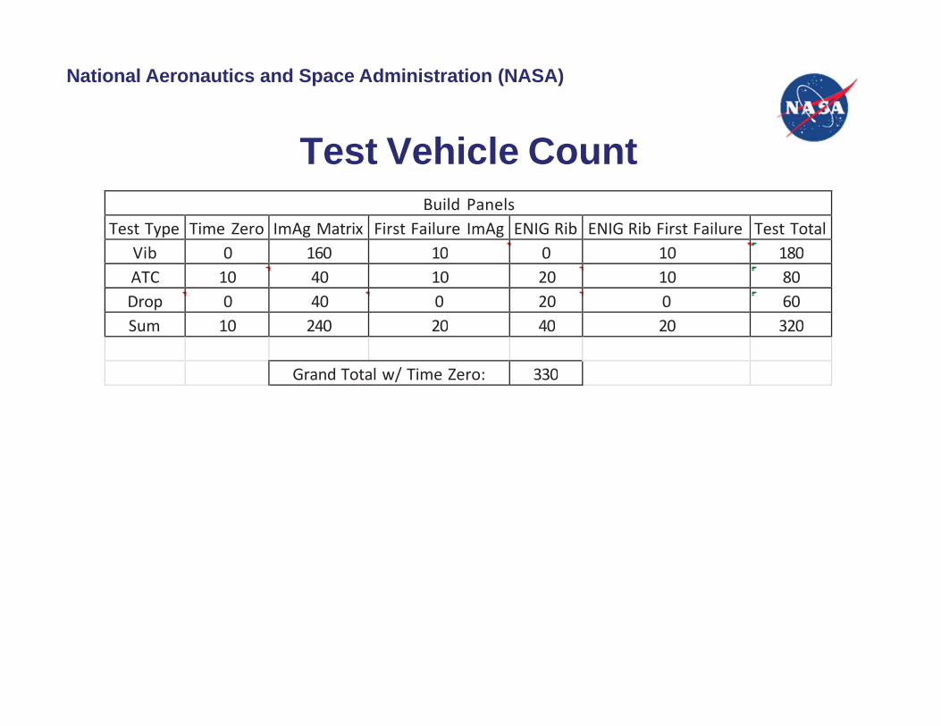
Test Vehicle Count
Build Panels
Test Type Time Zero ImAg Matrix First Failure ImAg ENIG Rib ENIG Rib First Failure Test TotalVib 0 160 10 0 10 180
ATC 10 40 10 20 10 80
Drop 0 40 0 20 0 60
Sum 10 240 20 40 20 320
Grand Total w/ Time Zero: 330
National Aeronautics and Space Administration (NASA)
Testing
• Thermal Cycle -55o/+125oC The thermal cycle testing determines the capability of a solder to withstand extreme thermal cycling.
• Vibration The vibration test determines solder joint failures during exposure to vibration conditions.
• Drop This test determines the resistance of board level interconnects to board strain induced by dynamic bending as a result of drop testing.
National Aeronautics and Space Administration (NASA)
Testing
• Copper Dissolution
National Aeronautics and Space Administration (NASA)
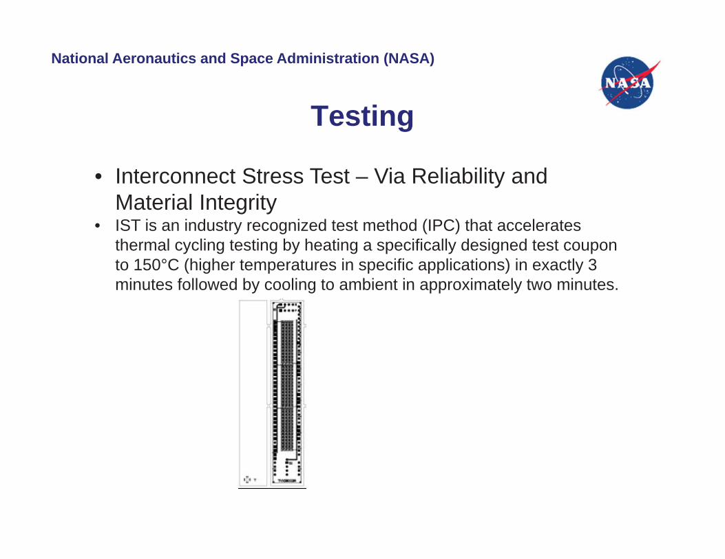
Testing
• Interconnect Stress Test – Via Reliability and Material Integrity
• IST is an industry recognized test method (IPC) that accelerates thermal cycling testing by heating a specifically designed test coupon to 150°C (higher temperatures in specific applications) in exactly 3 minutes followed by cooling to ambient in approximately two minutes.
National Aeronautics and Space Administration (NASA)
Websites
• NASA Scientific and Technical Information (STI) Program = http://www.sti.nasa.gov
• Technology Evaluation for Environmental Risk Mitigation (TEERM) Principal Center = http://teerm.nasa.gov
• IPC KAVI
National Aeronautics and Space Administration (NASA)
Questions