neo n703 wcdma module hardware user...
TRANSCRIPT
Neo_N703 WCDMA Module Hardware User Guide
Copyright © Neoway Technology Co., Ltd i
Neo_N703 WCDMA Module
Hardware User Guide
Version 1.0
Neo_N703 WCDMA Module Hardware User Guide
Copyright © Neoway Technology Co., Ltd i
Copyright © 2015 Neoway Technology Co., Ltd All right is reserved
is the trademark of Neoway Technology Co., Ltd.
All other trademarks and trade names mentioned in this document are the property of their respective
holders.
Remarks
This document is intended for system engineers (SEs), development engineers, and test engineers.
The information in this document is subject to change without notice due to product version update
or other reasons.
Every effort has been made in preparation of this document to ensure accuracy of the contents, but all
statements, information, and recommendations in this document do not constitute a warranty of any
kind, express or implied.
Neoway provides customers complete technical support. If you have any question, please contact
your account manager or email to
Website: http://www.neoway.com
Neo_N703 WCDMA Module Hardware User Guide
Copyright © Neoway Technology Co., Ltd ii
Contents
About This Document ......................................................................................................... 1
1 Introduction to N703 ......................................................................................................... 1
1.1 Overview ............................................................................................................................................ 1
1.2 Block Diagram ................................................................................................................................... 1
1.3 Features .............................................................................................................................................. 2
2 Pin Description and PCB Foot Print .............................................................................. 5
2.1 Specifications and Pin Definition ....................................................................................................... 5
2.2 Pin Description ................................................................................................................................... 6
2.3 PCB Foot Print ................................................................................................................................... 8
3 Power Control Interfaces ............................................................................................... 10
3.1 Power Supply Interfaces ................................................................................................................... 10
3.1.1 VBAT ...................................................................................................................................... 10
3.1.2 VDD_EXT .............................................................................................................................. 14
3.2 RESET .............................................................................................................................................. 14
3.3 PWRKEY ......................................................................................................................................... 15
4 Audio Interface ................................................................................................................ 17
4.1 Audio Input ....................................................................................................................................... 17
4.2 Audio Output .................................................................................................................................... 18
4.3 Audio Design Cautions ..................................................................................................................... 18
5 Peripheral Interfaces ....................................................................................................... 19
5.1 USB Interface ................................................................................................................................... 19
5.1.1 USB Connection ...................................................................................................................... 19
5.1.2 Sleep Mode Controlled by USB .............................................................................................. 20
5.2 UIM Card Interface .......................................................................................................................... 21
5.3 GPIO ................................................................................................................................................. 23
5.3.1 UART ...................................................................................................................................... 24
5.3.2 I2C ........................................................................................................................................... 25
5.3.3 SPI ........................................................................................................................................... 26
5.3.4 ADC ........................................................................................................................................ 26
5.3.5 NET_LIGHT ........................................................................................................................... 26
5.3.6 DTR ......................................................................................................................................... 27
5.3.7 RING Signal Indicator ............................................................................................................ 28
6 RF Interface ....................................................................................................................... 29
Neo_N703 WCDMA Module Hardware User Guide
Copyright © Neoway Technology Co., Ltd iii
7 Electric Feature and Reliability .................................................................................... 31
7.1 Electric Feature ................................................................................................................................. 31
7.2 Temperature ...................................................................................................................................... 31
7.3 ESD Protection ................................................................................................................................. 32
8 RF Feature ......................................................................................................................... 33
8.1 Work Band ........................................................................................................................................ 33
8.2 TX Power and RX Sensitivity .......................................................................................................... 33
9 Mounting and Packaging ............................................................................................... 35
9.1 Mounting the Module onto the Application Board ........................................................................... 35
9.2 Package ............................................................................................................................................. 35
10 Abbreviations ................................................................................................................. 36
Neo_N703 WCDMA Module Hardware User Guide
Copyright © Neoway Technology Co., Ltd iv
Table of Figures Figure 1-1 N703 block diagram ............................................................................................................... 2
Figure 2-1 Top view of N703 .................................................................................................................. 5
Figure 2-2 PCB foot print recommended for N703 ................................................................................. 9
Figure 3-1 Current peaks and voltage drops .......................................................................................... 10
Figure 3-2 Capacitors used for the power supply ...................................................................................11
Figure 3-3 Reference design of power supply control ............................................................................11
Figure 3-4 Reference design of power supply controlled by p-MOSFET ............................................. 12
Figure 3-5 Reference designs of separated power supply ...................................................................... 13
Figure 3-6 Reset controlled by button ................................................................................................... 14
Figure 3-7 Reset circuit with triode separating ...................................................................................... 14
Figure 3-8 Push switch controlling ........................................................................................................ 15
Figure 3-9 MCU controlling .................................................................................................................. 16
Figure 3-10 N703 power-on sequence ................................................................................................... 16
Figure 4-1 Reference design of MIC connection ................................................................................... 17
Figure 4-2 Reference design of SPK connections ................................................................................. 18
Figure 5-1 USB circuit .......................................................................................................................... 19
Figure 5-2 Sleep mode controlled by USB (a) ....................................................................................... 20
Figure 5-3 Sleep mode controlled by USB (b) ...................................................................................... 20
Figure 5-4 Reference design of SIM card interface ............................................................................... 22
Figure 5-5 Encapsulation ....................................................................................................................... 22
Figure 5-6 Reference design of the UART interface ............................................................................. 24
Figure 5-7 MCU 1.8V logic level .......................................................................................................... 24
Figure 5-8 Recommended circuit for the communication between 5V MCU and UART ..................... 25
Figure 5-9 Reference design of I2C ....................................................................................................... 25
Figure 5-10 Reference design of the SPI ............................................................................................... 26
Figure 5-11 LED indicator directly driven by high level ....................................................................... 27
Figure 5-12 LED indicator driven by transistor ..................................................................................... 27
Figure 5-13 RING indicator for incoming call ...................................................................................... 28
Figure 5-14 RING indicator for SMS .................................................................................................... 28
Figure 6-1 Reference of antenna matching design ................................................................................ 29
Figure 6-2 Encapsulation specifications of Murata RF connector ......................................................... 30
Figure 6-3 RF connections..................................................................................................................... 30
Neo_N703 WCDMA Module Hardware User Guide
Copyright © Neoway Technology Co., Ltd v
Table of Tables N703 baseband and wireless features ...................................................................................... 2
N703 dimensions ..................................................................................................................... 5
N703 pin description ................................................................................................................ 6
GPIO ...................................................................................................................................... 23
N703 Electric Feature ............................................................................................................ 31
Temperature Feature .............................................................................................................. 31
N703 ESD feature .................................................................................................................. 32
N703 work band .................................................................................................................... 33
N703 RF power and RX sensitivity ....................................................................................... 33
Neo_N703 WCDMA Module Hardware User Guide
Copyright © Neoway Technology Co., Ltd vi
Revision Record
Version Changes Revised By Date
V1.0 Initial draft Tian 2015-11
Neo_N703 WCDMA Module Hardware User Guide
Copyright © Neoway Technology Co., Ltd 1
About This Document
This document details the features, indicators, and reference standards of the N703 WCDMA module and
provides reference for the hardware design of each interface. This user guide can help you complete
wireless communication application easily.
1 Introduction to N703
1.1 Overview
N703 is a WCDMA module that supports multiple network modes including HSDPA, UMTS, EDGE,
GPRS, and GSM. For HSDPA, this module supports 3.6 Mbit/s for downlink data and 384 Kbit/s for
uplink data. N703 provides high-quality data and voice communication, SMS and other functions. It is
widely applied to electricity, Internet of Vehicle (IoV), video monitoring, handset devices, etc.
Cellular standards: HSDPA/UMTS/EDGE/GPRS/GSM
Windows, Android, and Linux drivers
Multiple-channel audio I/O
USB2.0/ADC/UART/SPI/I2C
1.2 Block Diagram
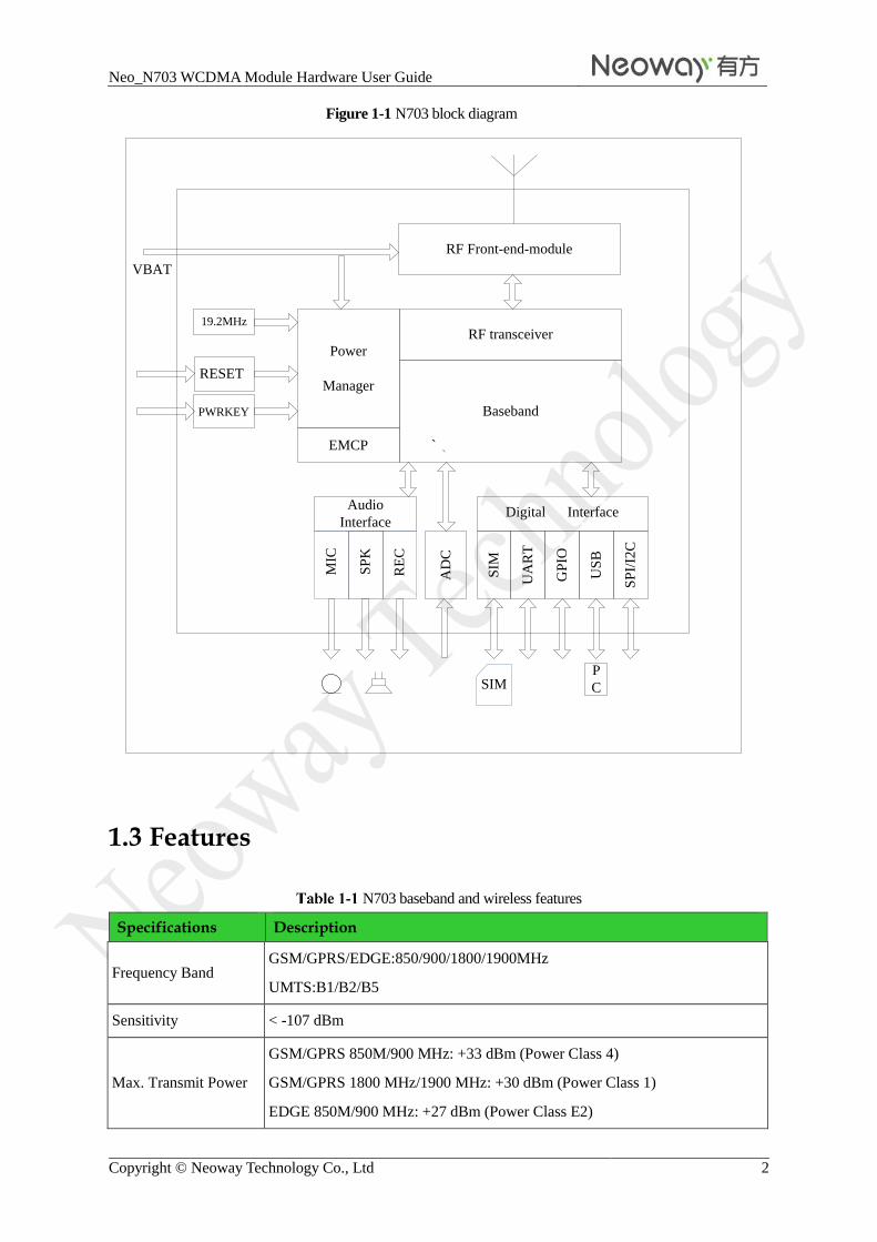
Figure 1-1 shows the block diagram of N703.
Neo_N703 WCDMA Module Hardware User Guide
Copyright © Neoway Technology Co., Ltd 2
Figure 1-1 N703 block diagram
VBAT
Digital Interface
GP
IO
US
B
SIM
UA
RT
PWRKEY
Power
Manager
RF transceiver
EMCP
19.2MHz
RF Front-end-module
Audio
Interface
MIC
SP
K
RE
C
AD
C
SIMP
C
SP
I/I2
C
``
Baseband
RESET
1.3 Features
N703 baseband and wireless features
Specifications Description
Frequency Band GSM/GPRS/EDGE:850/900/1800/1900MHz
UMTS:B1/B2/B5
Sensitivity < -107 dBm
Max. Transmit Power
GSM/GPRS 850M/900 MHz: +33 dBm (Power Class 4)
GSM/GPRS 1800 MHz/1900 MHz: +30 dBm (Power Class 1)
EDGE 850M/900 MHz: +27 dBm (Power Class E2)
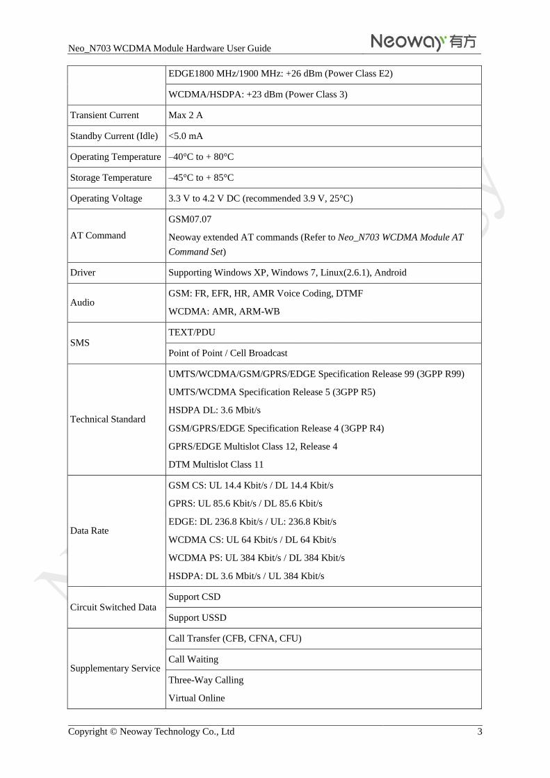
Neo_N703 WCDMA Module Hardware User Guide
Copyright © Neoway Technology Co., Ltd 3
EDGE1800 MHz/1900 MHz: +26 dBm (Power Class E2)
WCDMA/HSDPA: +23 dBm (Power Class 3)
Transient Current Max 2 A
Standby Current (Idle) <5.0 mA
Operating Temperature –40°C to + 80°C
Storage Temperature –45°C to + 85°C
Operating Voltage 3.3 V to 4.2 V DC (recommended 3.9 V, 25°C)
AT Command
GSM07.07
Neoway extended AT commands (Refer to Neo_N703 WCDMA Module AT
Command Set)
Driver Supporting Windows XP, Windows 7, Linux(2.6.1), Android
Audio GSM: FR, EFR, HR, AMR Voice Coding, DTMF
WCDMA: AMR, ARM-WB
SMS TEXT/PDU
Point of Point / Cell Broadcast
Technical Standard
UMTS/WCDMA/GSM/GPRS/EDGE Specification Release 99 (3GPP R99)
UMTS/WCDMA Specification Release 5 (3GPP R5)
HSDPA DL: 3.6 Mbit/s
GSM/GPRS/EDGE Specification Release 4 (3GPP R4)
GPRS/EDGE Multislot Class 12, Release 4
DTM Multislot Class 11
Data Rate
GSM CS: UL 14.4 Kbit/s / DL 14.4 Kbit/s
GPRS: UL 85.6 Kbit/s / DL 85.6 Kbit/s
EDGE: DL 236.8 Kbit/s / UL: 236.8 Kbit/s
WCDMA CS: UL 64 Kbit/s / DL 64 Kbit/s
WCDMA PS: UL 384 Kbit/s / DL 384 Kbit/s
HSDPA: DL 3.6 Mbit/s / UL 384 Kbit/s
Circuit Switched Data Support CSD
Support USSD
Supplementary Service
Call Transfer (CFB, CFNA, CFU)
Call Waiting
Three-Way Calling
Virtual Online
Neo_N703 WCDMA Module Hardware User Guide
Copyright © Neoway Technology Co., Ltd 4
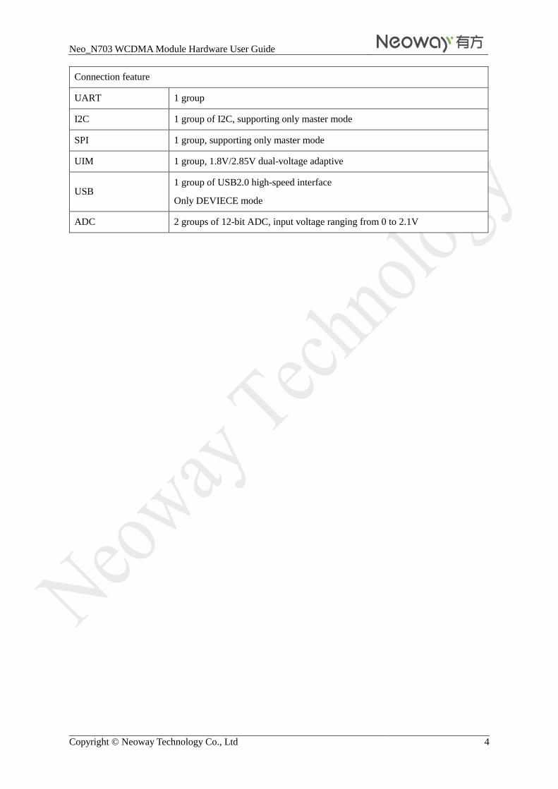
Connection feature
UART 1 group
I2C 1 group of I2C, supporting only master mode
SPI 1 group, supporting only master mode
UIM 1 group, 1.8V/2.85V dual-voltage adaptive
USB 1 group of USB2.0 high-speed interface
Only DEVIECE mode
ADC 2 groups of 12-bit ADC, input voltage ranging from 0 to 2.1V
Neo_N703 WCDMA Module Hardware User Guide
Copyright © Neoway Technology Co., Ltd 5
2 Pin Description and PCB Foot Print
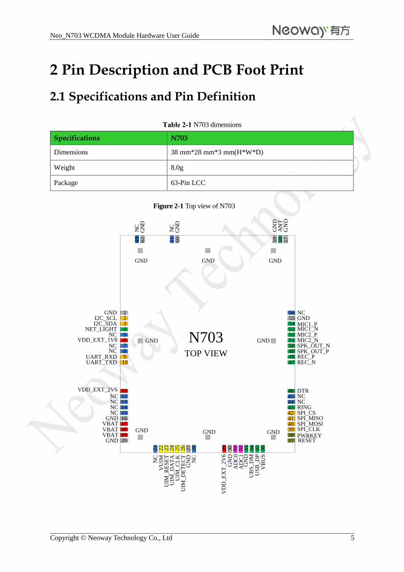
2.1 Specifications and Pin Definition
N703 dimensions
Specifications N703
Dimensions 38 mm*28 mm*3 mm(H*W*D)
Weight 8.0g
Package 63-Pin LCC
Figure 2-1 Top view of N703
1
32
456789
10
11
1314151617181920
21
22
23
24
25
26
27
28
29
30
31
32
33
34
35
36
37383940414243444546
47484950515253545556
57
58
59
60
61
62
63
GND
GND
GND GND GND
GND
GNDGNDGND
GND
GND
MIC1_P
GN
D
GN
D
GN
D
GN
D
I2C_SCLI2C_SDA
NET_LIGHTNC
VDD_EXT_1V8NCNC
UART_RXDUART_TXD
VDD_EXT_2V6
NCNCNCNC
VBATVBATVBAT
NC
NC
AN
T
NC
VU
IMU
IM_R
ES
ET
UIM
_D
AT
A
UIM
_D
ET
EC
TU
IM_C
LK
NC
GN
D
AD
C0
UB
S_D
MU
SB
_D
PV
BU
S
RESETPWRKEYSPI_CLKSPI_MOSISPI_MISOSPI_CSRINGNCNCDTR
NCGND
MIC1_NMIC2_PMIC2_NSPK_OUT_NSPK_OUT_PREC_PREC_N
N703TOP VIEW
12
VD
D_E
XT
_2V
6
GN
D
GN
D
AD
C1
Neo_N703 WCDMA Module Hardware User Guide
Copyright © Neoway Technology Co., Ltd 6
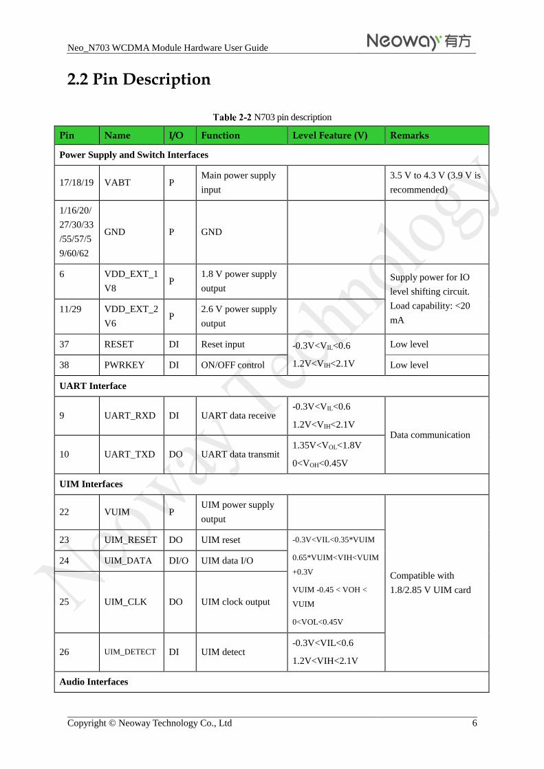
2.2 Pin Description
N703 pin description
Pin Name I/O Function Level Feature (V) Remarks
Power Supply and Switch Interfaces
17/18/19 VABT P Main power supply
input
3.5 V to 4.3 V (3.9 V is
recommended)
1/16/20/
27/30/33
/55/57/5
9/60/62
GND P GND
6 VDD_EXT_1
V8 P
1.8 V power supply
output Supply power for IO
level shifting circuit.
Load capability: <20
mA
11/29 VDD_EXT_2
V6 P
2.6 V power supply
output
37 RESET DI Reset input -0.3V<VIL<0.6
1.2V<VIH<2.1V
Low level
38 PWRKEY DI ON/OFF control Low level
UART Interface
9 UART_RXD DI UART data receive -0.3V<VIL<0.6
1.2V<VIH<2.1V Data communication
10 UART_TXD DO UART data transmit 1.35V<VOL<1.8V
0<VOH<0.45V
UIM Interfaces
22 VUIM P UIM power supply
output
Compatible with
1.8/2.85 V UIM card
23 UIM_RESET DO UIM reset -0.3V<VIL<0.35*VUIM
0.65*VUIM<VIH<VUIM
+0.3V
VUIM -0.45 < VOH <
VUIM
0<VOL<0.45V
24 UIM_DATA DI/O UIM data I/O
25 UIM_CLK DO UIM clock output
26 UIM_DETECT DI UIM detect -0.3V<VIL<0.6
1.2V<VIH<2.1V
Audio Interfaces
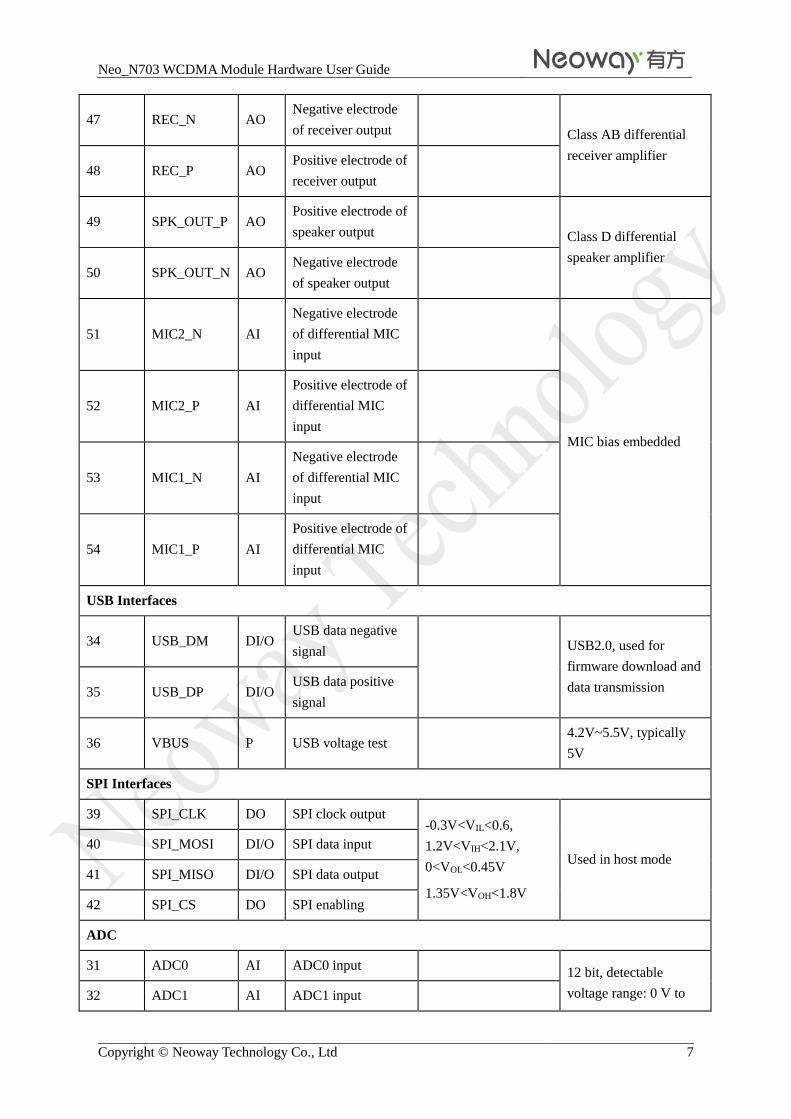
Neo_N703 WCDMA Module Hardware User Guide
Copyright © Neoway Technology Co., Ltd 7
47 REC_N AO Negative electrode
of receiver output
Class AB differential
receiver amplifier 48 REC_P AO
Positive electrode of
receiver output
49 SPK_OUT_P AO Positive electrode of
speaker output
Class D differential
speaker amplifier 50 SPK_OUT_N AO
Negative electrode
of speaker output
51 MIC2_N AI
Negative electrode
of differential MIC
input
MIC bias embedded
52 MIC2_P AI
Positive electrode of
differential MIC
input
53 MIC1_N AI
Negative electrode
of differential MIC
input
54 MIC1_P AI
Positive electrode of
differential MIC
input
USB Interfaces
34 USB_DM DI/O USB data negative
signal
USB2.0, used for
firmware download and
data transmission 35 USB_DP DI/O USB data positive
signal
36 VBUS P USB voltage test 4.2V~5.5V, typically
5V
SPI Interfaces
39 SPI_CLK DO SPI clock output -0.3V<VIL<0.6,
1.2V<VIH<2.1V,
0<VOL<0.45V
1.35V<VOH<1.8V
Used in host mode 40 SPI_MOSI DI/O SPI data input
41 SPI_MISO DI/O SPI data output
42 SPI_CS DO SPI enabling
ADC
31 ADC0 AI ADC0 input 12 bit, detectable
voltage range: 0 V to 32 ADC1 AI ADC1 input
Neo_N703 WCDMA Module Hardware User Guide
Copyright © Neoway Technology Co., Ltd 8
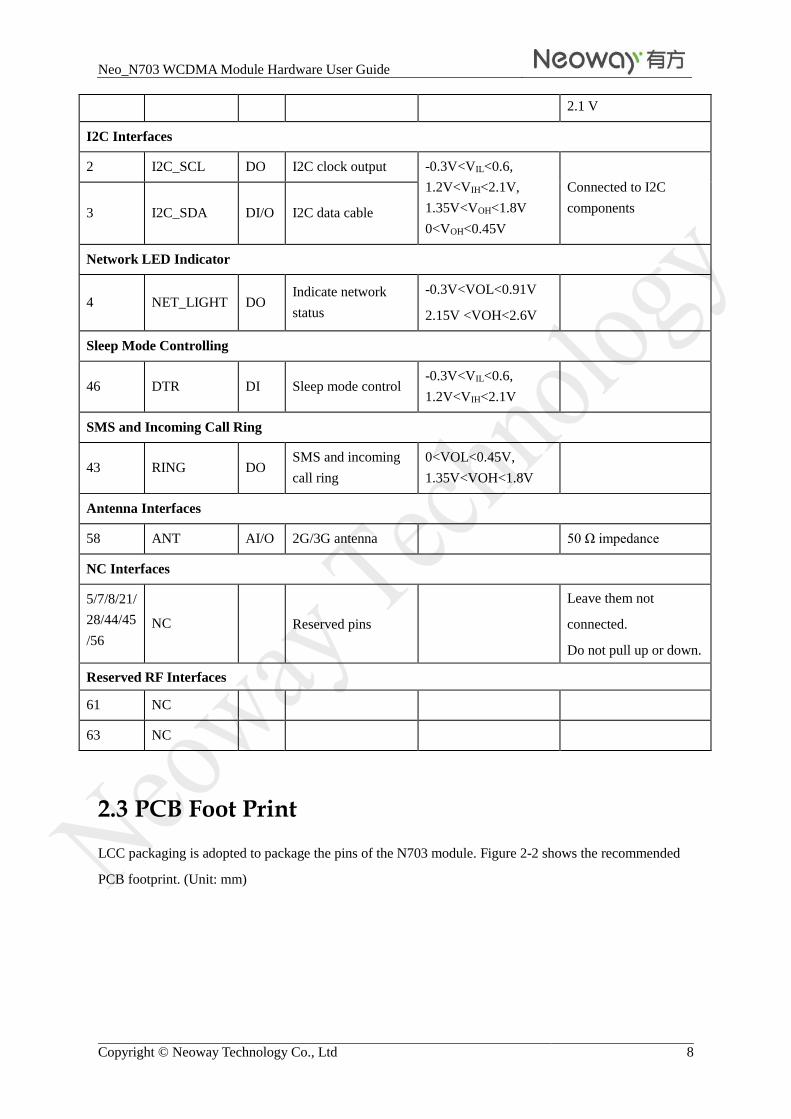
2.1 V
I2C Interfaces
2 I2C_SCL DO I2C clock output -0.3V<VIL<0.6,
1.2V<VIH<2.1V,
1.35V<VOH<1.8V
0<VOH<0.45V
Connected to I2C
components 3 I2C_SDA DI/O I2C data cable
Network LED Indicator
4 NET_LIGHT DO Indicate network
status
-0.3V<VOL<0.91V
2.15V <VOH<2.6V
Sleep Mode Controlling
46 DTR DI Sleep mode control -0.3V<VIL<0.6,
1.2V<VIH<2.1V
SMS and Incoming Call Ring
43 RING DO SMS and incoming
call ring
0<VOL<0.45V,
1.35V<VOH<1.8V
Antenna Interfaces
58 ANT AI/O 2G/3G antenna 50 Ω impedance
NC Interfaces
5/7/8/21/
28/44/45
/56
NC Reserved pins
Leave them not
connected.
Do not pull up or down.
Reserved RF Interfaces
61 NC
63 NC
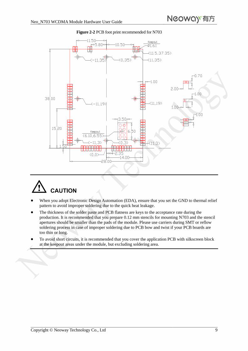
2.3 PCB Foot Print
LCC packaging is adopted to package the pins of the N703 module. Figure 2-2 shows the recommended
PCB footprint. (Unit: mm)
Neo_N703 WCDMA Module Hardware User Guide
Copyright © Neoway Technology Co., Ltd 9
Figure 2-2 PCB foot print recommended for N703
When you adopt Electronic Design Automation (EDA), ensure that you set the GND to thermal relief
pattern to avoid improper soldering due to the quick heat leakage.
The thickness of the solder paste and PCB flatness are keys to the acceptance rate during the
production. It is recommended that you prepare 0.12 mm stencils for mounting N703 and the stencil
apertures should be smaller than the pads of the module. Please use carriers during SMT or reflow
soldering process in case of improper soldering due to PCB bow and twist if your PCB boards are
too thin or long.
To avoid short circuits, it is recommended that you cover the application PCB with silkscreen block
at the keepout areas under the module, but excluding soldering area.
Neo_N703 WCDMA Module Hardware User Guide
Copyright © Neoway Technology Co., Ltd 10
3 Power Control Interfaces
Pin Name I/O Function Remarks
17/18/19 VABT P Main power
supply input 3.5 V to 4.3 V (3.9 V is recommended)
6 VDD_EXT_1V8 P 1.8 V power
supply output
Supply power for IO level shifting circuit.
Load capability: <20 mA
11/29 VDD_EXT_2V6 P 2.6 V power
supply output
Supply power for IO level shifting circuit.
Load capability: <20 mA
37 RESET DI Reset input Low level
38 PWRKEY DI ON/OFF control Low level
3.1 Power Supply Interfaces
3.1.1 VBAT
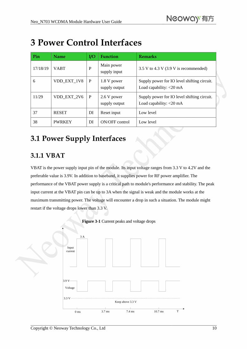
VBAT is the power supply input pin of the module. Its input voltage ranges from 3.3 V to 4.2V and the
preferable value is 3.9V. In addition to baseband, it supplies power for RF power amplifier. The
performance of the VBAT power supply is a critical path to module's performance and stability. The peak
input current at the VBAT pin can be up to 3A when the signal is weak and the module works at the
maximum transmitting power. The voltage will encounter a drop in such a situation. The module might
restart if the voltage drops lower than 3.3 V.
Figure 3-1 Current peaks and voltage drops
Keep above 3.3 V
3.3 V
0 ms 3.7 ms 7.4 ms 10.7 ms T
3 A
Voltage
Input
current
3.9 V
Neo_N703 WCDMA Module Hardware User Guide
Copyright © Neoway Technology Co., Ltd 11
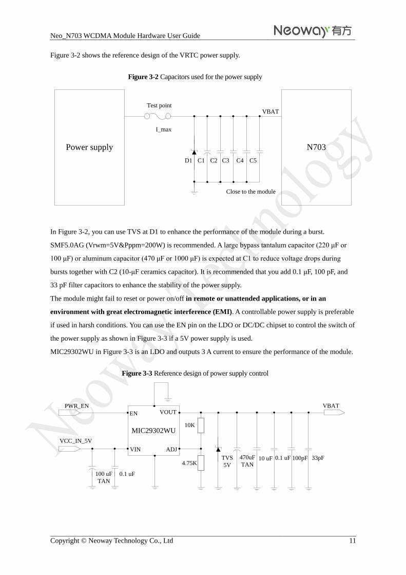
Figure 3-2 shows the reference design of the VRTC power supply.
Figure 3-2 Capacitors used for the power supply
N703
Close to the module
D1 C1 C2 C3 C4 C5
VBATTest point
I_max
Power supply
In Figure 3-2, you can use TVS at D1 to enhance the performance of the module during a burst.
SMF5.0AG (Vrwm=5V&Pppm=200W) is recommended. A large bypass tantalum capacitor (220 μF or
100 μF) or aluminum capacitor (470 μF or 1000 μF) is expected at C1 to reduce voltage drops during
bursts together with C2 (10-μF ceramics capacitor). It is recommended that you add 0.1 μF, 100 pF, and
33 pF filter capacitors to enhance the stability of the power supply.
The module might fail to reset or power on/off in remote or unattended applications, or in an
environment with great electromagnetic interference (EMI). A controllable power supply is preferable
if used in harsh conditions. You can use the EN pin on the LDO or DC/DC chipset to control the switch of
the power supply as shown in Figure 3-3 if a 5V power supply is used.
MIC29302WU in Figure 3-3 is an LDO and outputs 3 A current to ensure the performance of the module.
Figure 3-3 Reference design of power supply control
VCC_IN_5V
VBAT
100 uF
TAN
0.1 uF
TVS
5V10 uF470uF
TAN
10K
4.75K
VOUT
MIC29302WU
EN
VIN ADJ
0.1 uF 100pF 33pF
PWR_EN
Neo_N703 WCDMA Module Hardware User Guide
Copyright © Neoway Technology Co., Ltd 12
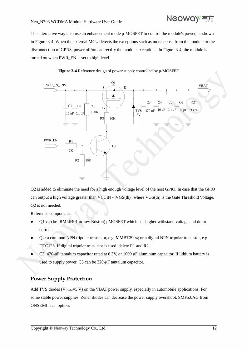
The alternative way is to use an enhancement mode p-MOSFET to control the module's power, as shown
in Figure 3-4. When the external MCU detects the exceptions such as no response from the module or the
disconnection of GPRS, power off/on can rectify the module exceptions. In Figure 3-4, the module is
turned on when PWR_EN is set to high level.
Figure 3-4 Reference design of power supply controlled by p-MOSFET
VCC_IN_3.9V VBAT
10K
100K33 pF10 uF
2K
10K
0.1 uF
Q1
R4C1 C2C4 C5 C7
R1
R2
10 uF 0.1 uF
R3
Q2
TVS
5V
470 uF
C3 C6
100pF
S
G
D
PWR_EN
Q2 is added to eliminate the need for a high enough voltage level of the host GPIO. In case that the GPIO
can output a high voltage greater than VCCIN - |VGS(th)|, where VGS(th) is the Gate Threshold Voltage,
Q2 is not needed.
Reference components:
Q1 can be IRML6401 or low Rds(on) pMOSFET which has higher withstand voltage and drain
current.
Q2: a common NPN tripolar transistor, e.g. MMBT3904; or a digital NPN tripolar transistor, e.g.
DTC123. If digital tripolar transistor is used, delete R1 and R2.
C3: 470-μF tantalum capacitor rated at 6.3V, or 1000 μF aluminum capacitor. If lithium battery is
used to supply power, C3 can be 220-μF tantalum capacitor.
Power Supply Protection
Add TVS diodes (VRWM=5 V) on the VBAT power supply, especially in automobile applications. For
some stable power supplies, Zener diodes can decrease the power supply overshoot. SMF5.0AG from
ONSEMI is an option.
Neo_N703 WCDMA Module Hardware User Guide
Copyright © Neoway Technology Co., Ltd 13
Line Rules
The width of primary loop lines for VBAT on PCB must be able to support the safe transmission of 2 A
current and ensure no obvious loop voltage decrease. Therefore, the loop line width of VBAT is required 2
mm and the ground level should be as complete as possible.
Separation
The module works in burst mode that generates voltage drops on power supply. Furthermore, this results
in a 217Hz TDD noise through power (One of the way generating noise. Another way is through RF
radiation). Analog parts, especially the audio circuits, are subjected to this noise, known as a "buzz noise"
in GSM systems. To prevent other parts from being affected, it is better to use separated power supplies.
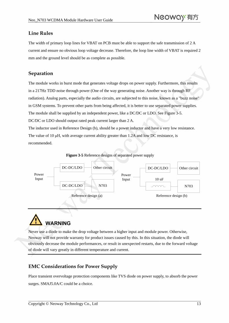
The module shall be supplied by an independent power, like a DC/DC or LDO. See Figure 3-5.
DC/DC or LDO should output rated peak current larger than 2 A.
The inductor used in Reference Design (b), should be a power inductor and have a very low resistance.
The value of 10 μH, with average current ability greater than 1.2A and low DC resistance, is
recommended.
Figure 3-5 Reference designs of separated power supply
Other circuitDC-DC/LDO
N703DC-DC/LDO
Power
Input
Other circuitDC-DC/LDO
N703
Power
Input 10 uF
Reference design (a) Reference design (b)
Never use a diode to make the drop voltage between a higher input and module power. Otherwise,
Neoway will not provide warranty for product issues caused by this. In this situation, the diode will
obviously decrease the module performances, or result in unexpected restarts, due to the forward voltage
of diode will vary greatly in different temperature and current.
EMC Considerations for Power Supply
Place transient overvoltage protection components like TVS diode on power supply, to absorb the power
surges. SMAJ5.0A/C could be a choice.
Neo_N703 WCDMA Module Hardware User Guide
Copyright © Neoway Technology Co., Ltd 14
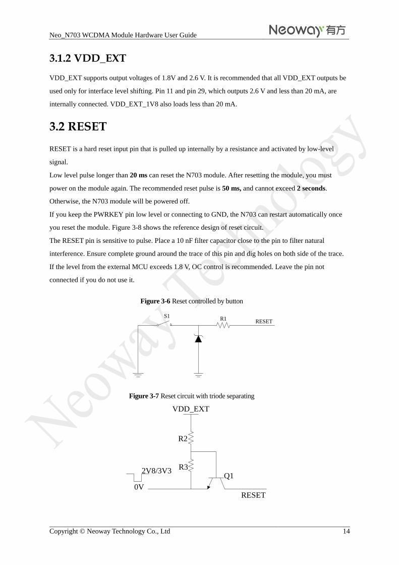
3.1.2 VDD_EXT
VDD_EXT supports output voltages of 1.8V and 2.6 V. It is recommended that all VDD_EXT outputs be
used only for interface level shifting. Pin 11 and pin 29, which outputs 2.6 V and less than 20 mA, are
internally connected. VDD_EXT_1V8 also loads less than 20 mA.
3.2 RESET
RESET is a hard reset input pin that is pulled up internally by a resistance and activated by low-level
signal.
Low level pulse longer than 20 ms can reset the N703 module. After resetting the module, you must
power on the module again. The recommended reset pulse is 50 ms, and cannot exceed 2 seconds.
Otherwise, the N703 module will be powered off.
If you keep the PWRKEY pin low level or connecting to GND, the N703 can restart automatically once
you reset the module. Figure 3-8 shows the reference design of reset circuit.
The RESET pin is sensitive to pulse. Place a 10 nF filter capacitor close to the pin to filter natural
interference. Ensure complete ground around the trace of this pin and dig holes on both side of the trace.
If the level from the external MCU exceeds 1.8 V, OC control is recommended. Leave the pin not
connected if you do not use it.
Figure 3-6 Reset controlled by button
RESETR1
S1
Figure 3-7 Reset circuit with triode separating
RESET
2V8/3V3R3
R2
0V
VDD_EXT
Q1
Neo_N703 WCDMA Module Hardware User Guide
Copyright © Neoway Technology Co., Ltd 15
In a circuit shown in Figure 3-7, VDD_EXT=2.8V/3.3V/3.0V, R2=4.7K, R3=47K.
If the module works in complicated environment, it might encounter halt or other abnormities. Therefore,
you must consider automatic restore when designing your products. The following two methods are
recommended:
Control the RESET pin (emergency shutdown) so that you can set low level for hard shutdown.
Perform the soft shutdown process by referring to Neo_N703 WCDMA Module AT Command Set.
Five seconds later, power off or reset the module. Otherwise, the program might be damaged during
the hard shutdown if the module is reading or writing information in the memory.
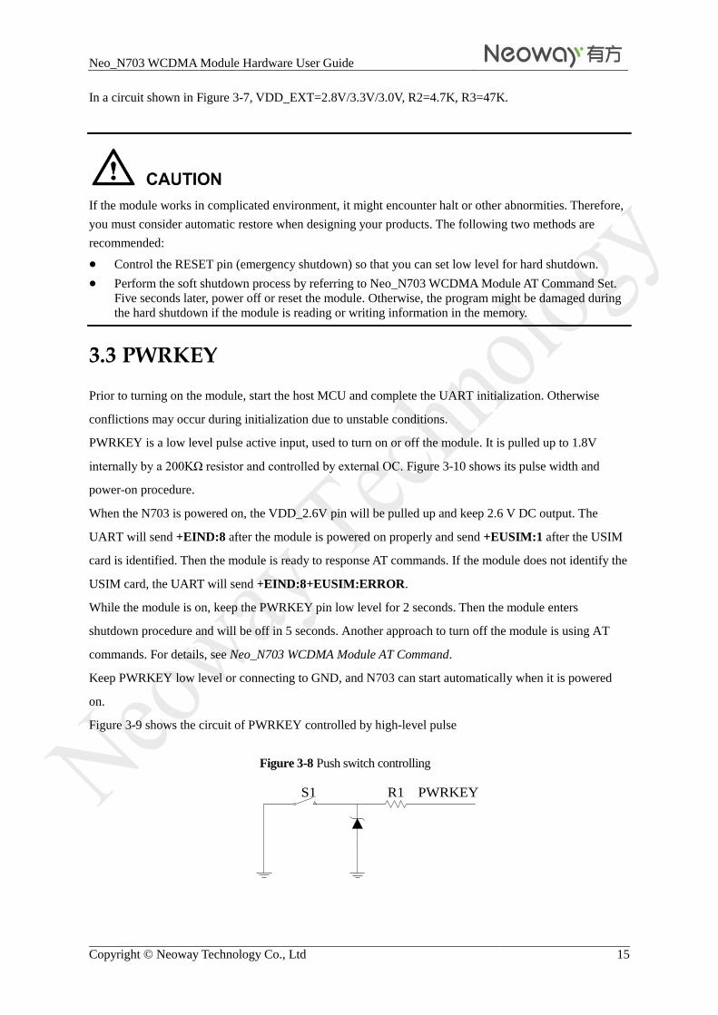
3.3 PWRKEY
Prior to turning on the module, start the host MCU and complete the UART initialization. Otherwise
conflictions may occur during initialization due to unstable conditions.
PWRKEY is a low level pulse active input, used to turn on or off the module. It is pulled up to 1.8V
internally by a 200KΩ resistor and controlled by external OC. Figure 3-10 shows its pulse width and
power-on procedure.
When the N703 is powered on, the VDD_2.6V pin will be pulled up and keep 2.6 V DC output. The
UART will send +EIND:8 after the module is powered on properly and send +EUSIM:1 after the USIM
card is identified. Then the module is ready to response AT commands. If the module does not identify the
USIM card, the UART will send +EIND:8+EUSIM:ERROR.
While the module is on, keep the PWRKEY pin low level for 2 seconds. Then the module enters
shutdown procedure and will be off in 5 seconds. Another approach to turn off the module is using AT
commands. For details, see Neo_N703 WCDMA Module AT Command.
Keep PWRKEY low level or connecting to GND, and N703 can start automatically when it is powered
on.
Figure 3-9 shows the circuit of PWRKEY controlled by high-level pulse
Figure 3-8 Push switch controlling
PWRKEYR1S1
Neo_N703 WCDMA Module Hardware User Guide
Copyright © Neoway Technology Co., Ltd 16
Figure 3-9 MCU controlling
USER_ONPWRKEY
R3
R2
If the module is powered on but the power-on sequence has not been completed, the states of each pin are
uncertain. The power-on sequence of the module is shown as Figure 3-10.
Figure 3-10 N703 power-on sequence
VBAT
PWRKEY
RESET
0.5s<t<1s 1.6V<VH
VL<0.5V
USB_DP
2.5s<t<5s
Power_on Procedure Power _ off
4s 4.6s
Procedure
The PWRKEY pin might encounter pulse interference generated by ESD. It is recommended that you
parallel a 10 nF capacitor connected to the ground to protect the PWRKEY pin.
It is not recommended that you connect the PWRKEY pin to ground to start the module because it will
affect the ESD feature of the module.
The ON_PWRKEY pin can control the module startup and shutdown. Do not repeat triggering this pin.
Otherwise, the startup or shutdown might fail. For example, the user plans to start up the module but gives
low-level pulse for twice, resulting in shutdown.
The shutdown function of the PWRKEY pin is controlled by the software. If the software is not running
properly, the module cannot shut down properly.
Neo_N703 WCDMA Module Hardware User Guide
Copyright © Neoway Technology Co., Ltd 17
4 Audio Interface
N703 provides two groups of audio input interfaces and two groups of output interfaces to meet your
requirements in different applications.
Pin Name I/O Function Remarks
47 REC_N AO Negative electrode of receiver output Class AB differential
receiver amplifier 48 REC_P AO Positive electrode of receiver output
49 SPK_OUT_P AO Positive electrode of speaker output Class D differential
speaker amplifier 50 SPK_OUT_N AO Negative electrode of speaker output
51 MIC2_N AI Negative electrode of differential MIC input
MIC bias embedded 52 MIC2_P AI Positive electrode of differential MIC input
53 MIC1_N AI Negative electrode of differential MIC input
54 MIC1_P AI Positive electrode of differential MIC input
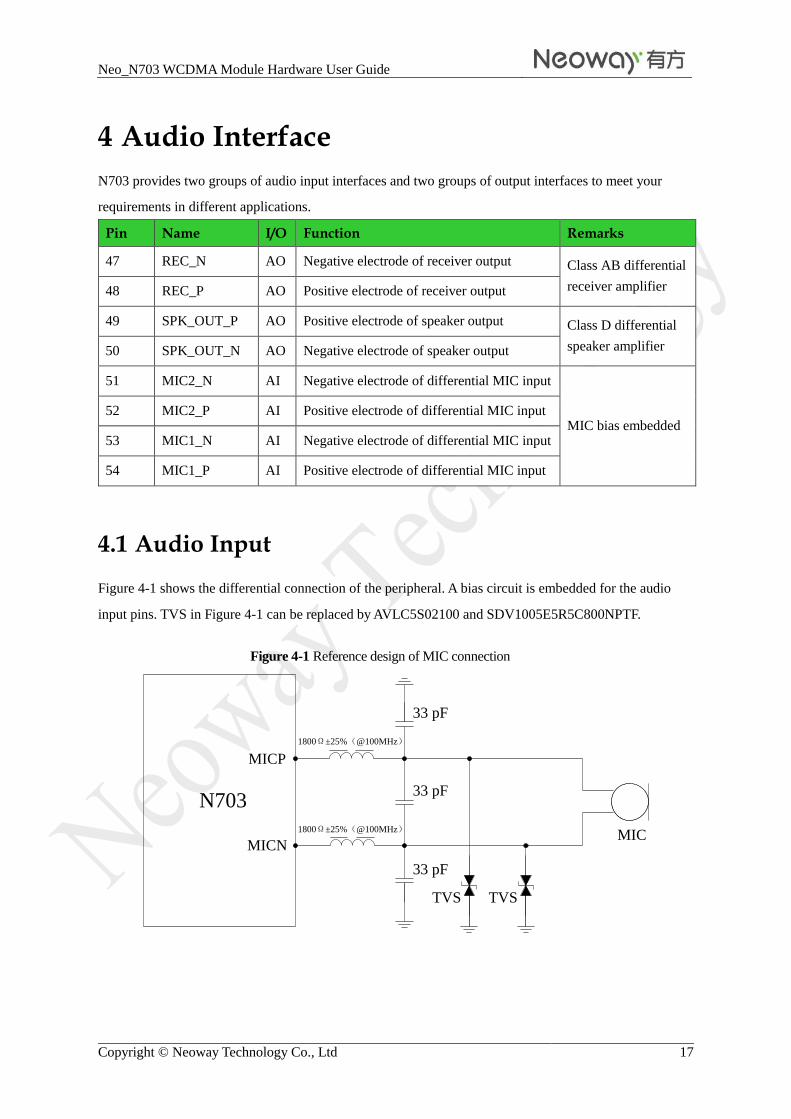
4.1 Audio Input
Figure 4-1 shows the differential connection of the peripheral. A bias circuit is embedded for the audio
input pins. TVS in Figure 4-1 can be replaced by AVLC5S02100 and SDV1005E5R5C800NPTF.
Figure 4-1 Reference design of MIC connection
N703
33 pF
MIC
33 pF
33 pF
MICN
MICP
TVS TVS
1800Ω±25%(@100MHz)
1800Ω±25%(@100MHz)
Neo_N703 WCDMA Module Hardware User Guide
Copyright © Neoway Technology Co., Ltd 18
4.2 Audio Output
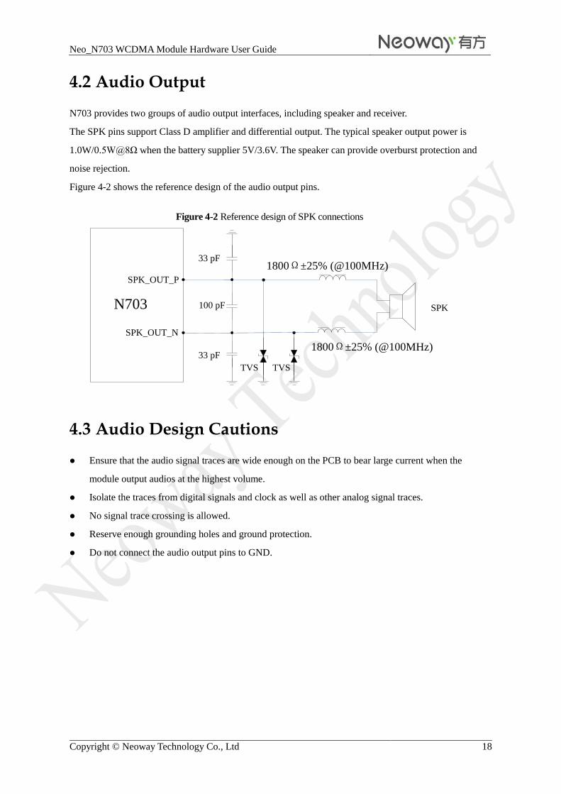
N703 provides two groups of audio output interfaces, including speaker and receiver.
The SPK pins support Class D amplifier and differential output. The typical speaker output power is
1.0W/0.5W@8Ω when the battery supplier 5V/3.6V. The speaker can provide overburst protection and
noise rejection.
Figure 4-2 shows the reference design of the audio output pins.
Figure 4-2 Reference design of SPK connections
33 pF
33 pF
SPK_OUT_N
SPK_OUT_P
100 pF SPK
1800Ω±25% (@100MHz)
1800Ω±25% (@100MHz)
TVSTVS
N703
4.3 Audio Design Cautions
Ensure that the audio signal traces are wide enough on the PCB to bear large current when the
module output audios at the highest volume.
Isolate the traces from digital signals and clock as well as other analog signal traces.
No signal trace crossing is allowed.
Reserve enough grounding holes and ground protection.
Do not connect the audio output pins to GND.
Neo_N703 WCDMA Module Hardware User Guide
Copyright © Neoway Technology Co., Ltd 19
5 Peripheral Interfaces
5.1 USB Interface
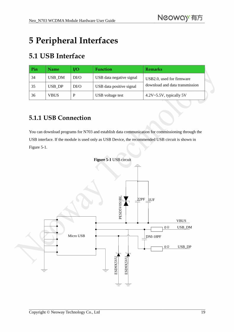
Pin Name I/O Function Remarks
34 USB_DM DI/O USB data negative signal USB2.0, used for firmware
download and data transmission 35 USB_DP DI/O USB data positive signal
36 VBUS P USB voltage test 4.2V~5.5V, typically 5V
5.1.1 USB Connection
You can download programs for N703 and establish data communication for commissioning through the
USB interface. If the module is used only as USB Device, the recommended USB circuit is shown in
Figure 5-1.
Figure 5-1 USB circuit
Micro USB
VBUS
22PF
ES
D9X
5V
U
ES
D9X
5V
U
PE
SD
5V
0S
1B
L
DNI-18PF
0Ω
0Ω
USB_DM
USB_DP
1UF
Neo_N703 WCDMA Module Hardware User Guide
Copyright © Neoway Technology Co., Ltd 20
Parallel a 1μF and 22pF filter capacitors to the VBUS pin as close to the pin as possible. TVS components
are required for the VBUS power line. The junction capacitance of the TVS protection diodes for
USB_DP and USB_DM should be lower than 12pF as possible. USB data lines adopt differential trace
design, in which the differential impedance is limited to 90 Ω characteristics impedance. Isolate the traces
from other signal traces.
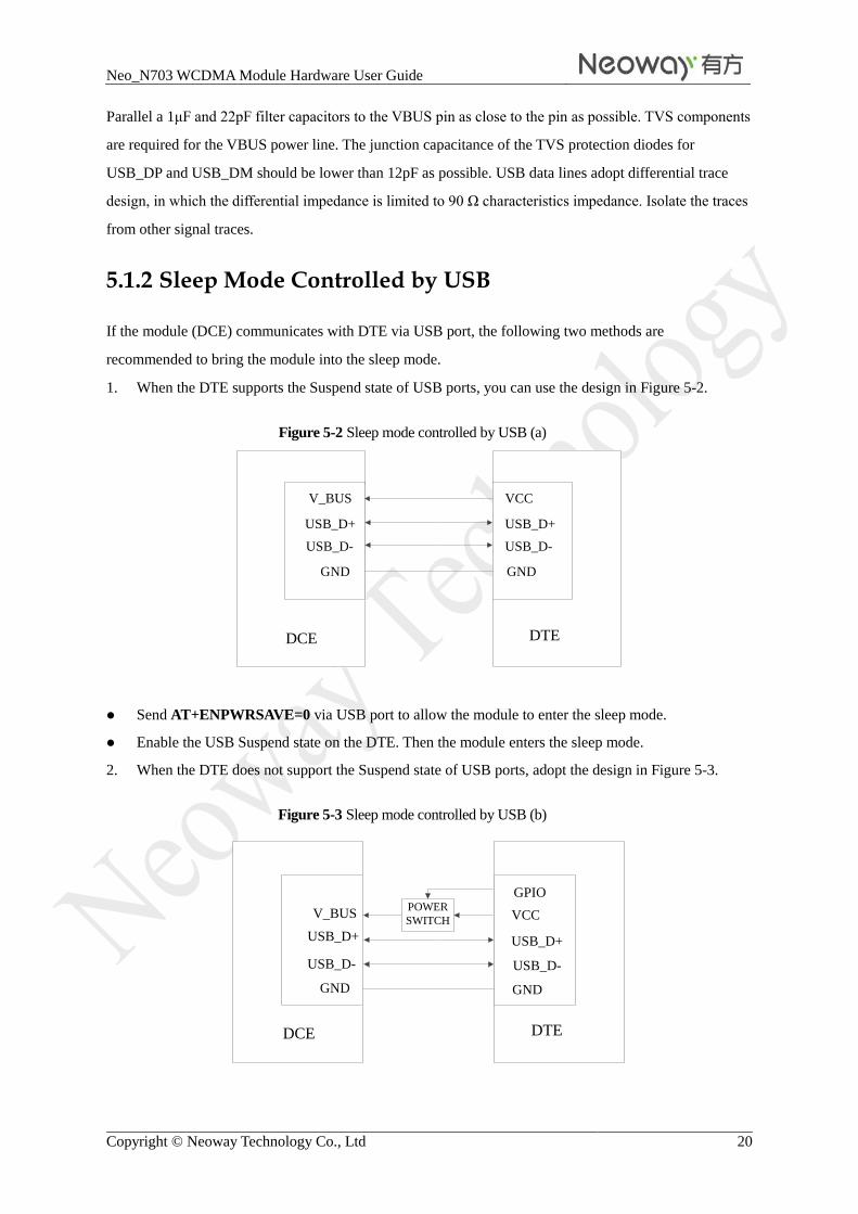
5.1.2 Sleep Mode Controlled by USB
If the module (DCE) communicates with DTE via USB port, the following two methods are
recommended to bring the module into the sleep mode.
1. When the DTE supports the Suspend state of USB ports, you can use the design in Figure 5-2.
Figure 5-2 Sleep mode controlled by USB (a)
Send AT+ENPWRSAVE=0 via USB port to allow the module to enter the sleep mode.
Enable the USB Suspend state on the DTE. Then the module enters the sleep mode.
2. When the DTE does not support the Suspend state of USB ports, adopt the design in Figure 5-3.
Figure 5-3 Sleep mode controlled by USB (b)
V_BUS
USB_D+
USB_D-
VCC
USB_D+
USB_D-
GND GND
DTEDCE
V_BUS
USB_D+
USB_D-
VCC
USB_D+
USB_D-
GND GND
DTEDCE
GPIOPOWER
SWITCH
Neo_N703 WCDMA Module Hardware User Guide
Copyright © Neoway Technology Co., Ltd 21
Send AT+ENPWRSAVE=0 via USB to allow the module to enter the sleep mode.
The DTE controls the sleep mode of the module by controlling the power supply via GPIO. If the
power supply is switched off, the module enters the sleep mode; if the power supply is on, the
module will be woken up.
The response takes 6.0s when the module is standby after registering to the network. The response
time is 6.0s if there is no data service after the module sets up a TCP connection.
The module can receives voice, SMS, and other messages in the sleep mode enabled by UART and USB.
It wakes up automatically upon receiving SMS, voice, or data. Then you can send AT commands. The
module enters the sleep mode again after all services are over.
The USB circuit design should comply with the USB 2.0.
The traces of USB_D+ and USB_D- must be routed as a group of differential pair with 90 Ω
differential impedance.
The USB differential pair should be routed side-by-side and on the same layer.
USB_D+ and USB_D- is a pair of high speed signals, so the trace lengths should match as well as
possible.
USB interface must be connected or set aside the relevant test points to facilitate subsequent
firmware upgrade or debugging.
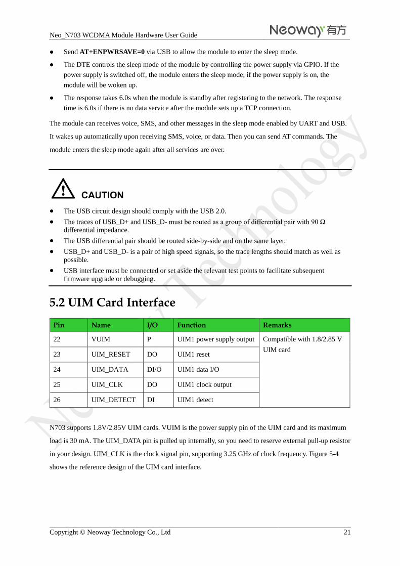
5.2 UIM Card Interface
Pin Name I/O Function Remarks
22 VUIM P UIM1 power supply output Compatible with 1.8/2.85 V
UIM card 23 UIM_RESET DO UIM1 reset
24 UIM_DATA DI/O UIM1 data I/O
25 UIM_CLK DO UIM1 clock output
26 UIM_DETECT DI UIM1 detect
N703 supports 1.8V/2.85V UIM cards. VUIM is the power supply pin of the UIM card and its maximum
load is 30 mA. The UIM_DATA pin is pulled up internally, so you need to reserve external pull-up resistor
in your design. UIM_CLK is the clock signal pin, supporting 3.25 GHz of clock frequency. Figure 5-4
shows the reference design of the UIM card interface.
Neo_N703 WCDMA Module Hardware User Guide
Copyright © Neoway Technology Co., Ltd 22
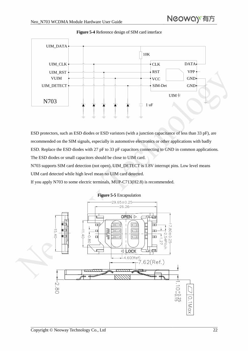
Figure 5-4 Reference design of SIM card interface
1 uF
UIM_DATA
UIM_CLK
UIM_RST
VUIM
N703
CLK
RST
VCC
VPP
GND
UIM卡
DATA
GNDSIM-DetUIM_DETECT
10K
ESD protectors, such as ESD diodes or ESD varistors (with a junction capacitance of less than 33 pF), are
recommended on the SIM signals, especially in automotive electronics or other applications with badly
ESD. Replace the ESD diodes with 27 pF to 33 pF capacitors connecting to GND in common applications.
The ESD diodes or small capacitors should be close to UIM card.
N703 supports SIM card detection (not open). UIM_DETECT is 1.8V interrupt pins. Low level means
UIM card detected while high level mean no UIM card detected.
If you apply N703 to some electric terminals, MUP-C713(H2.8) is recommended.
Figure 5-5 Encapsulation
Neo_N703 WCDMA Module Hardware User Guide
Copyright © Neoway Technology Co., Ltd 23
The antenna should be installed far away from the UIM card and UIM card traces, especially to the
build-in antenna.
The UIM traces on the PCB should be as short as possible and shielded with GND copper.
The ESD protection diodes or small capacitors should be close to UIM card on the PCB.
5.3 GPIO
N703 supports multiple standards including UART, I2C, and SPI. You can configure the GPIO to meet
your requirements for connecting to different devices. For the open multi-function GPIO interface, please
inquiry our technical support engineers. The level of the module interface is 1.8 V. Table 5-1 lists GPIO
pins.
GPIO
Pin Name I/O Function Remarks
9 UART_RXD DI UART data receive Data communication
10 UART_TXD DO UART data transmit
39 SPI_CLK DO SPI clock output
Used in host mode 40 SPI_MOSI DI/O SPI data input
41 SPI_MISO DI/O SPI data output
42 SPI_CS DO SPI enabling
31 ADC0 AI ADC0 input 12 bit, detectable voltage
range: 0 V to 2.1 V 32 ADC1 AI ADC1 input
2 I2C_SCL DO I2C clock output Connected to I2C
components 3 I2C_SDA DI/O I2C data cable
4 NET_LIGHT DO Indicate network status Output 1.8V
46 DTR DI Sleep mode control
43 RING DO SMS and incoming call ring
Neo_N703 WCDMA Module Hardware User Guide
Copyright © Neoway Technology Co., Ltd 24
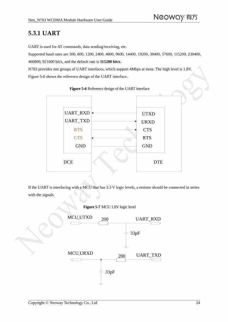
5.3.1 UART
UART is used for AT commands, data sending/receiving, etc.
Supported baud rates are 300, 600, 1200, 2400, 4800, 9600, 14400, 19200, 38400, 57600, 115200, 230400,
460800, 921600 bit/s, and the default rate is 115200 bit/s.
N703 provides one groups of UART interfaces, which support 4Mbps at most. The high level is 1.8V.
Figure 5-6 shows the reference design of the UART interface.
Figure 5-6 Reference design of the UART interface
UART_RXD
RTS
CTS
UTXD
URXD
CTS
RTS
GND GND
DTEDCE
UART_TXD
If the UART is interfacing with a MCU that has 3.3 V logic levels, a resistor should be connected in series
with the signals.
Figure 5-7 MCU 1.8V logic level
200
33 pF
33 pF
MCU_UTXD
MCU_URXD
200 UART_RXD
UART_TXD
Neo_N703 WCDMA Module Hardware User Guide
Copyright © Neoway Technology Co., Ltd 25
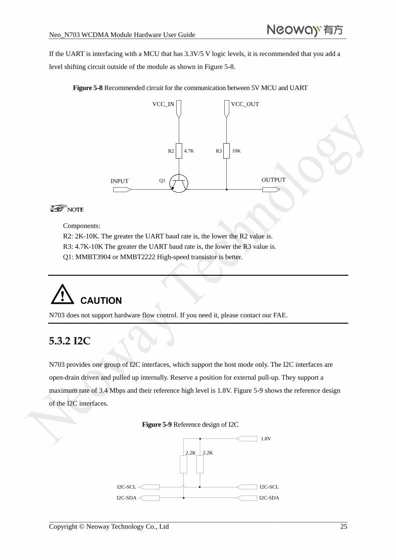
If the UART is interfacing with a MCU that has 3.3V/5 V logic levels, it is recommended that you add a
level shifting circuit outside of the module as shown in Figure 5-8.
Figure 5-8 Recommended circuit for the communication between 5V MCU and UART
OUTPUT
VCC_IN VCC_OUT
4.7K 10KR2 R3
INPUT Q1
Components:
R2: 2K-10K. The greater the UART baud rate is, the lower the R2 value is.
R3: 4.7K-10K The greater the UART baud rate is, the lower the R3 value is.
Q1: MMBT3904 or MMBT2222 High-speed transistor is better.
N703 does not support hardware flow control. If you need it, please contact our FAE.
5.3.2 I2C
N703 provides one group of I2C interfaces, which support the host mode only. The I2C interfaces are
open-drain driven and pulled up internally. Reserve a position for external pull-up. They support a
maximum rate of 3.4 Mbps and their reference high level is 1.8V. Figure 5-9 shows the reference design
of the I2C interfaces.
Figure 5-9 Reference design of I2C
2.2K 2.2K
1.8V
I2C-SCL
I2C-SDA
I2C-SCL
I2C-SDA
Neo_N703 WCDMA Module Hardware User Guide
Copyright © Neoway Technology Co., Ltd 26
5.3.3 SPI
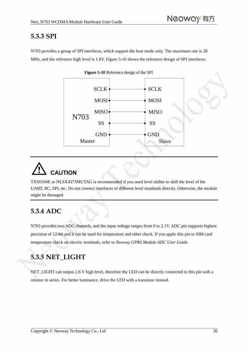
N703 provides a group of SPI interfaces, which support the host mode only. The maximum rate is 26
MHz, and the reference high level is 1.8V. Figure 5-10 shows the reference design of SPI interfaces.
Figure 5-10 Reference design of the SPI
SCLK
SS
MISON703
MOSI
GND
Master
SCLK
SS
MISO
MOSI
GND
Slave
TXS0104E or NLSX4373MUTAG is recommended if you need level shifter to shift the level of the
UART, IIC, SPI, etc. Do not connect interfaces of different level standards directly. Otherwise, the module
might be damaged.
5.3.4 ADC
N703 provides two ADC channels, and the input voltage ranges from 0 to 2.1V. ADC pin supports highest
precision of 12-bit and it can be used for temperature and other check. If you apply this pin to SIM card
temperature check on electric terminals, refer to Neoway GPRS Module ADC User Guide.
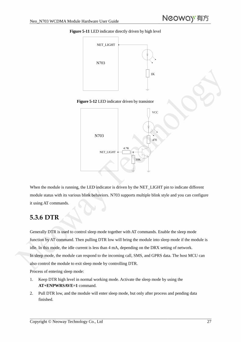
5.3.5 NET_LIGHT
NET_LIGHT can output 2.6 V high level, therefore the LED can be directly connected to this pin with a
resistor in series. For better luminance, drive the LED with a transistor instead.
Neo_N703 WCDMA Module Hardware User Guide
Copyright © Neoway Technology Co., Ltd 27
Figure 5-11 LED indicator directly driven by high level
NET_LIGHT
N703
1K
Figure 5-12 LED indicator driven by transistor
NET_LIGHT
N703
10K
VCC
4.7K
470
When the module is running, the LED indicator is driven by the NET_LIGHT pin to indicate different
module status with its various blink behaviors. N703 supports multiple blink style and you can configure
it using AT commands.
5.3.6 DTR
Generally DTR is used to control sleep mode together with AT commands. Enable the sleep mode
function by AT command. Then pulling DTR low will bring the module into sleep mode if the module is
idle. In this mode, the idle current is less than 4 mA, depending on the DRX setting of network.
In sleep mode, the module can respond to the incoming call, SMS, and GPRS data. The host MCU can
also control the module to exit sleep mode by controlling DTR.
Process of entering sleep mode:
1. Keep DTR high level in normal working mode. Activate the sleep mode by using the
AT+ENPWRSAVE=1 command.
2. Pull DTR low, and the module will enter sleep mode, but only after process and pending data
finished.
Neo_N703 WCDMA Module Hardware User Guide
Copyright © Neoway Technology Co., Ltd 28
3. In sleep mode, the external MCP can pull DTR high so that the module will exit from sleep mode
actively. Then the module can transmit data and initiate calls. After processing is finished, pull DTR
low again to take the module back to sleep mode.
4. In sleep mode, the module can be woken up by the events of incoming voice call, received data, or
SMS. Meanwhile the module will send out the unsolicited messages through the UART.
Upon receipt of the unsolicited messages, the host MCU should pull DTR high firstly, otherwise the
module will resume sleep mode in two minutes after the service processing. Then the host MCU can
process the voice call, received data, or SMS. After processing is finished, pull DTR low again to put
the module into sleep mode.
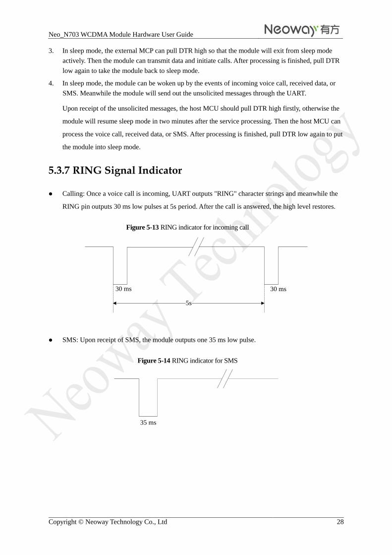
5.3.7 RING Signal Indicator
Calling: Once a voice call is incoming, UART outputs "RING" character strings and meanwhile the
RING pin outputs 30 ms low pulses at 5s period. After the call is answered, the high level restores.
Figure 5-13 RING indicator for incoming call
SMS: Upon receipt of SMS, the module outputs one 35 ms low pulse.
Figure 5-14 RING indicator for SMS
5s
30 ms 30 ms
35 ms
Neo_N703 WCDMA Module Hardware User Guide
Copyright © Neoway Technology Co., Ltd 29
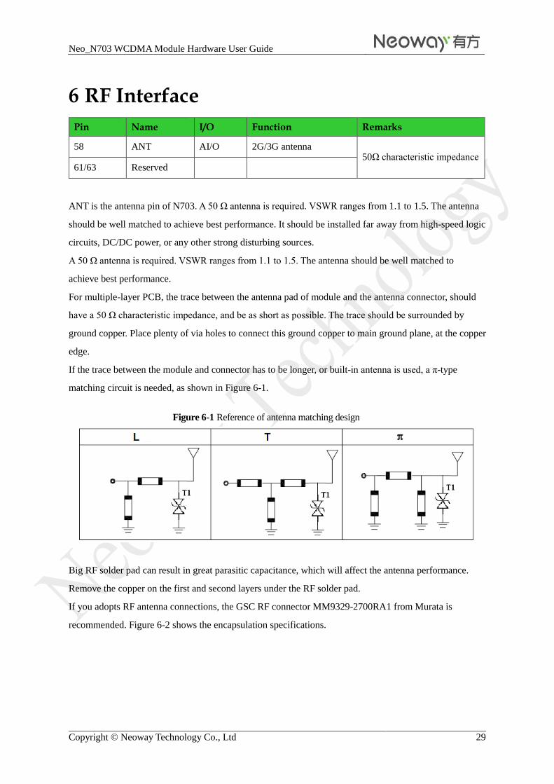
6 RF Interface
Pin Name I/O Function Remarks
58 ANT AI/O 2G/3G antenna 50Ω characteristic impedance
61/63 Reserved
ANT is the antenna pin of N703. A 50 Ω antenna is required. VSWR ranges from 1.1 to 1.5. The antenna
should be well matched to achieve best performance. It should be installed far away from high-speed logic
circuits, DC/DC power, or any other strong disturbing sources.
A 50 Ω antenna is required. VSWR ranges from 1.1 to 1.5. The antenna should be well matched to
achieve best performance.
For multiple-layer PCB, the trace between the antenna pad of module and the antenna connector, should
have a 50 Ω characteristic impedance, and be as short as possible. The trace should be surrounded by
ground copper. Place plenty of via holes to connect this ground copper to main ground plane, at the copper
edge.
If the trace between the module and connector has to be longer, or built-in antenna is used, a π-type
matching circuit is needed, as shown in Figure 6-1.
Figure 6-1 Reference of antenna matching design
Big RF solder pad can result in great parasitic capacitance, which will affect the antenna performance.
Remove the copper on the first and second layers under the RF solder pad.
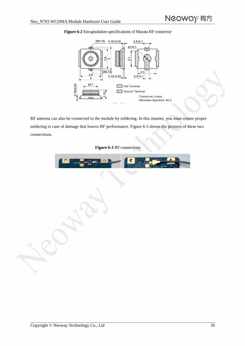
If you adopts RF antenna connections, the GSC RF connector MM9329-2700RA1 from Murata is
recommended. Figure 6-2 shows the encapsulation specifications.
Neo_N703 WCDMA Module Hardware User Guide
Copyright © Neoway Technology Co., Ltd 30
Figure 6-2 Encapsulation specifications of Murata RF connector
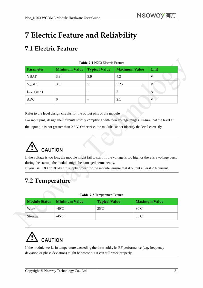
RF antenna can also be connected to the module by soldering. In this manner, you must ensure proper
soldering in case of damage that lowers RF performance. Figure 6-3 shows the pictures of these two
connections.
Figure 6-3 RF connections
Neo_N703 WCDMA Module Hardware User Guide
Copyright © Neoway Technology Co., Ltd 31
7 Electric Feature and Reliability
7.1 Electric Feature
N703 Electric Feature
Refer to the level design circuits for the output pins of the module.
For input pins, design their circuits strictly complying with their voltage ranges. Ensure that the level at
the input pin is not greater than 0.5 V. Otherwise, the module cannot identify the level correctly.
If the voltage is too low, the module might fail to start. If the voltage is too high or there is a voltage burst
during the startup, the module might be damaged permanently.
If you use LDO or DC-DC to supply power for the module, ensure that it output at least 2 A current.
7.2 Temperature
Temperature Feature
Module Status Minimum Value Typical Value Maximum Value
Work -40 25 80
Storage -45 85
If the module works in temperature exceeding the thresholds, its RF performance (e.g. frequency
deviation or phase deviation) might be worse but it can still work properly.
Parameter Minimum Value Typical Value Maximum Value Unit
VBAT 3.3 3.9 4.2 V
V_BUS 3.3 5 5.25 V
IMAX (start) - - 2 A
ADC 0 - 2.1 V
Neo_N703 WCDMA Module Hardware User Guide
Copyright © Neoway Technology Co., Ltd 32
7.3 ESD Protection
Electronics need to pass sever ESD tests. The following table shows the ESD capability of key pins of our
module. It is recommended that you add ESD protection to those pins in accordance to the application to
ensure your product quality when designing your products.
Humility: 45%Temperature: 25
N703 ESD feature
Testing Point Contact Discharge Air Discharge
VBAT ±8KV ±15KV
GND ±8KV ±15KV
ANT ±8KV ±15KV
Cover ±8KV ±15KV
Others ±4KV ±8KV
Neo_N703 WCDMA Module Hardware User Guide
Copyright © Neoway Technology Co., Ltd 33
8 RF Feature
8.1 Work Band
N703 work band
Work band Uplink Downlink
GSM 850 824–849 MHz 869–894 MHz
GSM 900 880–915 MHz 925–960 MHz
GSM 1800(DCS) 1770–1785MHz 1805–1880 MHz
GSM 1900(PCS) 1850–1910 MHz 1930–1990 MHz
WCDMA B1 (2100MHz) 1920~1980MHz 2110~2170MHz
WCDMA B2 (1900MHz) 1850MHz~1909MHz 1930MHz~1989MHz
WCDMA B5 (850MHz) 824MHz~849MHz 869MHz~894MHz
8.2 TX Power and RX Sensitivity
N703 RF power and RX sensitivity
Band Transmitting Power Receiving Sensitivity
WCDMA B1 (2100MHz) 24dBm +1dBm/-3dBm <-107dBm
WCDMA B2 (1900MHz) 24dBm +1dBm/-3dBm <-107dBm
WCDMA B5 (850MHz) 24dBm +1dBm/-3dBm <-107dBm
GSM850 GMSK(1Tx Slot) 33 dBm+2/-2dBm <-107dBm
8PSK(1Tx Slot) 27 dBm+3/-3dBm <-107dBm
GSM900 GMSK(1Tx Slot) 33 dBm+2/-2dBm <-107dBm
8PSK(1Tx Slot) 27 dBm+3/-3dBm <-107dBm
GSM1800 GMSK(1Tx Slot) 30dBm+2/-2dBm <-107dBm
8PSK(1Tx Slot) 26dBm+3/-3dBm <-107dBm
GSM1900 GMSK(1Tx Slot) 30dBm+2/-2dBm <-107dBm
8PSK(1Tx Slot) 26dBm+3/-3dBm <-107dBm
Neo_N703 WCDMA Module Hardware User Guide
Copyright © Neoway Technology Co., Ltd 34
The data in the above tables is obtained by connecting the module to RF test instrument (e.g.
CMU200, CWM500, or Agilent 8960) in lab tests. It is for reference only.
Neo_N703 WCDMA Module Hardware User Guide
Copyright © Neoway Technology Co., Ltd 35
9 Mounting and Packaging
9.1 Mounting the Module onto the Application Board
N703 is compatible with industrial standard reflow profile for lead-free SMT process.
The reflow profile is process dependent, so the following recommendation is just a start point guideline:
Only one flow is supported.
Quality of the solder joint depends on the solder volume. Minimum of 0.1 mm stencil thickness is
recommended.
Use bigger aperture size of the stencil than actual pad size.
Use a low-residue, no-clean type solder paste.
For information about cautions in N703 storage and mounting, refer to Neoway Module Reflow
Manufacturing Recommendations.
When you maintain and manually solder it, use heat guns with great opening, adjust the temperature to
250 degrees (depending on the type of the solder paste), and heat the module till the solder paste is melt.
The remove the module using tweezers. Do not shake the module in high temperature when you remove it.
Otherwise, the components inside the module might be misplaced.
9.2 Package
N703 modules are packaged in sealed bags on delivery to guarantee a long shelf life. Package the modules
again in case of opening for any reasons.
If exposed in air for more than 48 hours at conditions not worse than 30°C/60% RH, a baking procedure
should be done before SMT. Or, if the indication card shows humidity greater than 20%, the baking
procedure is also required. Do not bake modules with the package tray directly.
Neo_N703 WCDMA Module Hardware User Guide
Copyright © Neoway Technology Co., Ltd 36
10 Abbreviations
ADC Analog-Digital Converter
AFC Automatic Frequency Control
AGC Automatic Gain Control
AMR Acknowledged multirate (speech coder)
CSD Circuit Switched Data
CPU Central Processing Unit
DAI Digital Audio interface
DAC Digital-to-Analog Converter
DCE Data Communication Equipment
DSP Digital Signal Processor
DTE Data Terminal Equipment
DTMF Dual Tone Multi-Frequency
DTR Data Terminal Ready
EFR Enhanced Full Rate
EGSM Enhanced GSM
EMC Electromagnetic Compatibility
EMI Electro Magnetic Interference
ESD Electronic Static Discharge
ETS European Telecommunication Standard
FDMA Frequency Division Multiple Access
FR Full Rate
GPRS General Packet Radio Service
GSM Global Standard for Mobile Communications
HR Half Rate
IC Integrated Circuit
IMEI International Mobile Equipment Identity
LCD Liquid Crystal Display
LED Light Emitting Diode
MS Mobile Station
Neo_N703 WCDMA Module Hardware User Guide
Copyright © Neoway Technology Co., Ltd 37
PCB Printed Circuit Board
PCS Personal Communication System
RAM Random Access Memory
RF Radio Frequency
ROM Read-only Memory
RMS Root Mean Square
RTC Real Time Clock
SIM Subscriber Identification Module
SMS Short Message Service
SRAM Static Random Access Memory
TA Terminal adapter
TDMA Time Division Multiple Access
UART Universal asynchronous receiver-transmitter
USSD Unstructured Supplementary Service Data
VSWR Voltage Standing Wave Ratio