optimization of quantum-dot molecular beam epitaxy for ... · optimization of quantum-dot molecular...
TRANSCRIPT

Optimization of Quantum-Dot Molecular Beam Epitaxy for Broad Spectral Bandwidth DevicesVolume 4, Number 6, December 2012
M. A. MajidM. HuguesS. VézianD. T. D. ChildsR. A. Hogg
DOI: 10.1109/JPHOT.2012.22251401943-0655/$31.00 ©2012 IEEE

Optimization of Quantum-Dot MolecularBeam Epitaxy for Broad Spectral
Bandwidth DevicesM. A. Majid,1;4 M. Hugues,2;3 S. Vezian,3
D. T. D. Childs,1 and R. A. Hogg1;2
1Department of Electronic and Electrical Engineering, The University of Sheffield,Centre for Nano-science and Technology, Sheffield S3 7HQ, U.K.
2EPSRC National Centre for III-V Technologies, Centre for Nano-science and Technology,Sheffield S3 7HQ, U.K.
3Centre de Recherche sur l’Hetero-Epitaxie et ses Applications (CRHEA-CNRS),Valbonne 06560, France
4Photonics Laboratory, Computer, Electrical, and Mathematical Sciences andEngineering (CEMSE) Division, King Abdullah University of Science &
Technology (KAUST), Thuwal 23955-6900, Saudi Arabia
DOI: 10.1109/JPHOT.2012.22251401943-0655/$31.00 �2012 IEEE
Manuscript received September 18, 2012; revised October 3, 2012; accepted October 10, 2012. Dateof publication October 18, 2012; date of current version November 13, 2012. Corresponding author:M. A. Majid (e-mail: [email protected]; [email protected]).
Abstract: The optimization of the key growth parameters for broad spectral bandwidthdevices based on quantum dots is reported. A combination of atomic force microscopy,photoluminescence of test samples, and optoelectronic characterization of superlumines-cent diodes (SLDs) is used to optimize the growth conditions to obtain high-quality deviceswith large spectral bandwidth, radiative efficiency (due to a reduced defective-dot density),and thus output power. The defective-dot density is highlighted as being responsible for thedegradation of device performance. An SLD device with 160 nm of bandwidth centered at1230 nm is demonstrated.
Index Terms: Growth parameters, quantum dot (QD), superluminescent diode (SLD),spectral bandwidth.
1. IntroductionOptical coherence tomography (OCT) is a well-established technique for cross-sectional imaging ofbiological specimens. A broadband light source is the crucial component of the OCT system [1], andthe development of compact and broadband optical sources in the region of 950–1350 nm hasgreat potential in ophthalmic imaging [2] (800–1100 nm; zero-dispersion in eye) and tissue imaging(1100–1350 nm; minimum absorption and scattering in skin) [3], [4]. For low cost and robust clinicalapplications, superluminescent diodes (SLDs) are an ideal light source. SLDs may outperformmore complex sources such as supercontinuum sources [1], swept laser sources [5], and thermalsources [6] in terms of cost, output power, and/or relative intensity noise. Traditionally, quantumwells act as the light generation and amplifying medium and have been employed to realize abroad optical spectrum of the SLD. Different techniques, such as multiplexed broadband SLDs [7],intermixed quantum wells [8], [9], SLDs integrated with tapered optical amplifiers [10], and chirpedmultiple quantum wells [11], [12], have been developed. However, in general, there is a tradeoffbetween optical power and spectral width due to a reduction in peak gain. Also, commercial
Vol. 4, No. 6, December 2012 Page 2066
IEEE Photonics Journal Optimization of QD Molecular Beam Epitaxy
quantum-well-based SLDs are limited to �100 nm of bandwidth in the 1000 to 1550 nm range,while larger bandwidths would be of benefit since they will increase the spatial resolution along theoptical axis.
Recently, SLDs with self-assembled quantum dots (QDs) have attracted huge interest as anactive element [13]. In contrast to QD lasers, dot-to-dot size inhomogeneity and gain saturation area distinct advantage to a QD SLD. In view of this, QD SLDs are typically operated at the currentdensity where the ground-state and excited-state power balances, with minimum spectral dip(G 3 dB). A spectral dip is undesirable due to the possibility of ghost images in OCT [14], and in anideal case, it should be eliminated. The majority of the development of QD epitaxy [high growthtemperature 9 500 �C and low growth rates of 0.01–0.05 monolayers (ML)/s are used to obtain anarrow ground-state linewidth] has focused on QD lasers, particularly the push to high-quality1300 nm QD lasers for application in optical communications [15]–[17]. However, for OCT of skintissue, the wavelength specifications are more relaxed (�1100–1300 nm) than those for opticalcommunications, with a wide spectral region being of interest. For broadband applications, a highQD density, high inhomogeneity, and high integrated modal gain is advantageous. As a result,the majority of existing epitaxial processes for active QD devices are not optimized for broadbandapplications.
In a preliminary study on optimization of QD growth parameters, we found that QD depositiontemperature is a key parameter for high-power broadband QD SLDs [18]. In this paper, we presenta detailed study of the growth conditions for QDs and their optimization for broad spectral bandwidthdevices. For this purpose, photoluminescence (PL) and atomic force microscopy (AFM)measurements on 1100 to 1300 nm QD-in-well (DWELL) test samples have been correlated withSLD characteristics. The reduction of QD growth temperature results in an increase in QD densityand inhomogeneity, but a concomitant increase in defective-island density. Broadening of thespectral bandwidth is observed but is accompanied by a strong reduction in device quality (reducedPL of test sample and electroluminescence (EL) efficiency, reduced reverse breakdown voltage,and reduced output power of the SLD). A reduction in defective-island density is obtained byreducing the amount of InAs, thus improving PL efficiency in test samples and allowing the recoveryof good device characteristics while maintaining a broad spectral bandwidth.
2. Experimental MethodsThe samples studied in this paper were grown by molecular beam epitaxy on 2-in n-type GaAs(100) substrates. The active region consists of six DWELL layers corresponding to the followinggrowth sequence: 1-nm-thick In0:15Ga0:85As, 2.6 ML of InAs to form QDs, 6-nm-thick In0:15Ga0:85Ascap layer, and further 5 nm of GaAs. For all the samples, the DWELL structures are separated by40-nm-thick GaAs grown at 580 �C. Unless indicated otherwise, the QDs are formed by depositing2.6 ML of InAs at a growth rate of 0.1 MLs�1. The details of epitaxial growth including the choice ofDWELL, composition, and growth parameters can be found in previous reports on QD laser epitaxydevelopment [15], [18], [19], [20]. Two kinds of samples with different DWELL growth temperatureshave been grown, i.e., test samples for AFM and PL measurements, and SLD samples foroptoelectronic characterization. For the test samples, the active layers are embedded in a 100-nm-thick undoped GaAs/AlGaAs heterostructure with an uncapped layer of QDs (on 1-nm-thickIn0:15Ga0:85As) on the sample surface. Special care has been taken by ramping down the growthtemperature as quickly as possible at the end of the growth in order to avoid/reduce the ripeningprocesses. For SLDs, doped cladding and contact layers have been added [15]. Broad-area SLDswere fabricated using conventional processing, and 6-mm-long and 50-�m-wide ridge devices wereused for optoelectronic characterization. All the devices were mounted on ceramic tiles and probeddirectly. The measurements were carried out at a tile temperature of 300 K, while pulsed operation(5 �s pulsed duration, 1% duty cycle) is used to minimize self-heating effects.
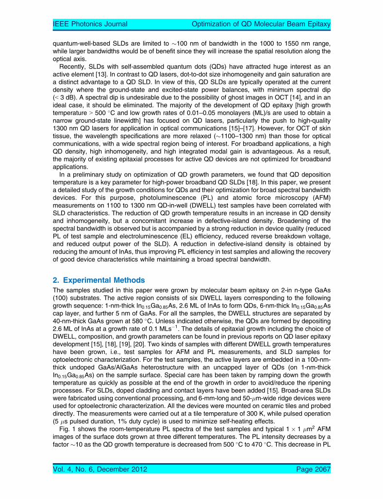
Fig. 1 shows the room-temperature PL spectra of the test samples and typical 1� 1 �m2 AFMimages of the surface dots grown at three different temperatures. The PL intensity decreases by afactor �10 as the QD growth temperature is decreased from 500 �C to 470 �C. This decrease in PL
IEEE Photonics Journal Optimization of QD Molecular Beam Epitaxy
Vol. 4, No. 6, December 2012 Page 2067
intensity indicates an increase in the density of nonradiative centers with decreasing growthtemperature. Their origins could be defective dots and/or larger Ga vacancy and As antisite den-sities induced by the lower growth temperature of the cap layer. For these samples, the emissionwavelength is roughly the same, shifting from 1290 nm to 1270 nm as the temperature decreases.The blueshift of the emission wavelength may be attributed to the decrease in size of the QDshighlighted by the AFM measurements [21].
As the QD growth temperature decreases from 500 �C to 470 �C, the AFM images show anincrease not only in the QD areal density but also in defective-island density. The defective islands(i.e., largest dot/island on the AFM images) result from the coalescence of several dots, which isgenerally accompanied by the generation of dislocations [21]–[23]. We observe an increase of afactor of �2 in QD density (8:7� 1010 cm�2 for 470 �C against 3:8� 1010 cm�2 at 500 �C) and anincrease of a factor of �12 (0:55� 108 at 500 �C to 6:5� 108 cm�2 at 470 �C) in defective-islanddensity as the growth temperature decreased from 500 �C to 470 �C. We note that this trend
Fig. 1. Room-temperature PL and 1� 1 �m2 AFM images obtained from InAs/GaAs DWELL grown at500 �C, 485 �C, and 470 �C.
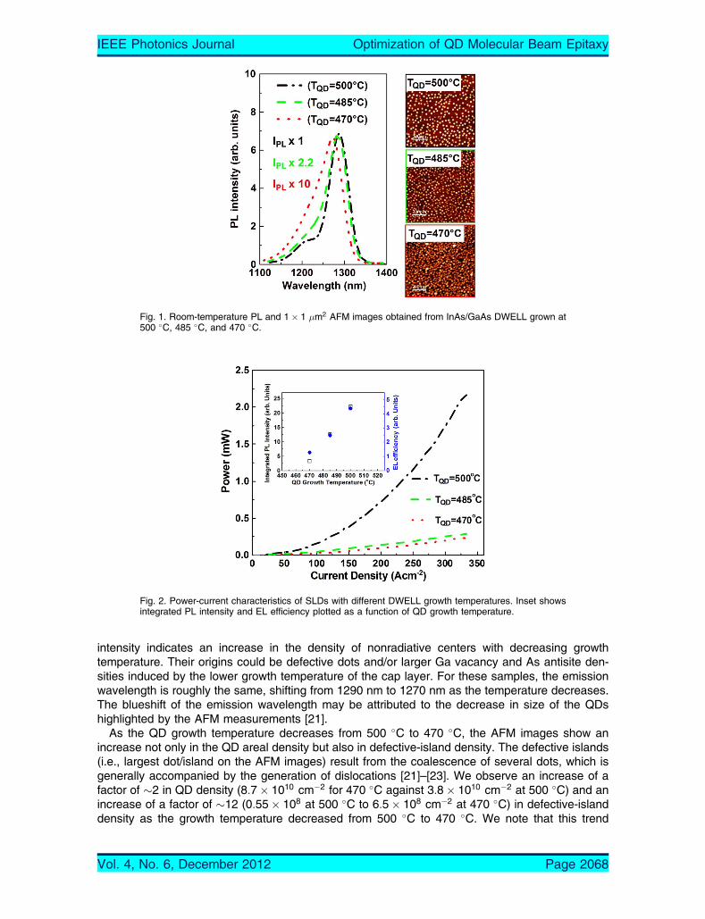
Fig. 2. Power-current characteristics of SLDs with different DWELL growth temperatures. Inset showsintegrated PL intensity and EL efficiency plotted as a function of QD growth temperature.
IEEE Photonics Journal Optimization of QD Molecular Beam Epitaxy
Vol. 4, No. 6, December 2012 Page 2068
continues to lower temperatures [24]. With an increase in QD areal density, an increase in room-temperature PL intensity is expected (same pumping intensity and PL structure used for all thesamples), but the larger defect density (defective islands) may overwhelm this beneficial effect.Although the increase of the dot density is highly desirable, the effect of the increase in defective-island density on device performances should be investigated. Fig. 2 shows the optical power-current density response measured from one facet of the SLD devices with the three differentDWELL growth temperatures discussed previously.
When the DWELLs are grown at 470 �C and 485 �C, the SLDs show limited superluminescencebehavior, thus suggesting limited gain. On the other hand, for DWELL growth temperature of 500 �C,superluminescent behavior is clearly evidenced by the superlinear increase in optical power. Atcurrent density of 330 Acm�2, a tenfold higher optical power is obtained when the DWELL is grown at500 �C. This result would have been surprising if one only considers the QD areal density. Indeed, forthe 500 �C grown DWELL, the areal density is less than half the one of the sample grown at 470 �C.However, the defective-island density increased by a factor of �12 as the growth temperature isreduced by 30 �C. An exploded view in Fig. 2 at low current density (not presented here) shows that
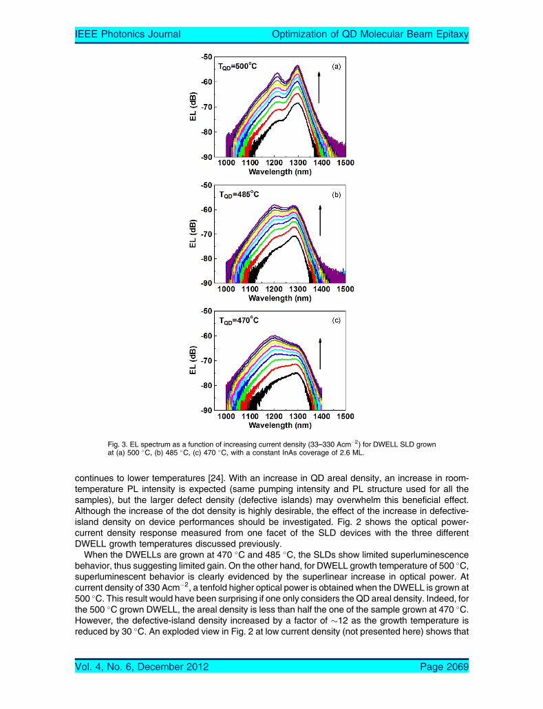
Fig. 3. EL spectrum as a function of increasing current density (33–330 Acm�2) for DWELL SLD grownat (a) 500 �C, (b) 485 �C, (c) 470 �C, with a constant InAs coverage of 2.6 ML.
IEEE Photonics Journal Optimization of QD Molecular Beam Epitaxy
Vol. 4, No. 6, December 2012 Page 2069
the spontaneous emission efficiency (SE) decreases with decreasing QD growth temperature. Thisstrong reduction of the SE could be correlated to the expected increase of the defect density (Gavacancy, As antisite) of the GaAs cap layer and the large increase in defective-island density. Thesedefective islands may act as nonradiative recombination centers that efficiently trap the carriers andthus reduce the carrier lifetime and SE efficiency, thus impacting on the ability to achieve gain(superluminescence) in the structure.
The inset in Fig. 2 plots the integrated PL intensity and EL efficiency, as a function of QD growthtemperature. The EL efficiency (is simply the slope efficiency of the optical power-current densityresponse) and integrated PL efficiency are calculated from Figs. 1 and 2, respectively. This figureshows that the EL efficiency of the SLD devices has good correlation with the integrated PLefficiency of the test structures. These results emphasize the strength of the combination of PL,AFM, and electrical characteristics in selecting a particular QD growth temperature.
Fig. 3 plots the EL spectra as a function of increasing current density for QD SLDs, grown at(a) 500 �C, (b) 485 �C, and (c) 470 �C. QD SLDs for broadband applications are typically operated atthe current density where the ground-state and excited-state power balances in order to provide themaximum spectral bandwidth. For QD SLD grown at 470 �C, a broad flat top emission spectraresulting from the balance of ground-state and excited-state contributions is observed. For the QDSLD grown at 500 �C and 485 �C, the QD ground state and excited state are quite well resolvedresulting in the appearance of a dip. Note that, for 500 �C grown SLD, the power balanced condition isnot obtained even for the highest current density. For the temperature range studied (500 �C–470 �C),a reduction in spectral dip with decreasing growth temperatures is observed. The AFM images showthat the dot dimensions decrease as the growth temperature is reduced. It is quite evident that, forsmaller dots, the influence of dot-to-dot size variation will be larger and so will induce a broaderemission of the dot ensemble. In consequence, since the linewidth of the ground and excited statesare broader, their overlap will be greater and allows the avoidance of the appearance of a spectral dip.In brief summary, the use of a low growth temperature could be of benefit for SLD applications sincehigh QD areal density and broad emission without a spectral dip have been demonstrated. However,the radiative efficiency becomes poor due to the increase of defective island. Further optimization isthus required to improve device quality, e.g., through reducing the coalesced island density.
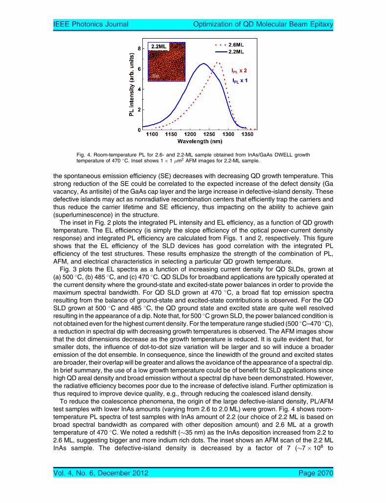
To reduce the coalescence phenomena, the origin of the large defective-island density, PL/AFMtest samples with lower InAs amounts (varying from 2.6 to 2.0 ML) were grown. Fig. 4 shows room-temperature PL spectra of test samples with InAs amount of 2.2 (our choice of 2.2 ML is based onbroad spectral bandwidth as compared with other deposition amount) and 2.6 ML at a growthtemperature of 470 �C. We noted a redshift (�35 nm) as the InAs deposition increased from 2.2 to2.6 ML, suggesting bigger and more indium rich dots. The inset shows an AFM scan of the 2.2 MLInAs sample. The defective-island density is decreased by a factor of 7 (�7� 108 to
Fig. 4. Room-temperature PL for 2.6- and 2.2-ML sample obtained from InAs/GaAs DWELL growthtemperature of 470 �C. Inset shows 1� 1 �m2 AFM images for 2.2-ML sample.
IEEE Photonics Journal Optimization of QD Molecular Beam Epitaxy
Vol. 4, No. 6, December 2012 Page 2070

�1� 108 cm�2) as the deposition amount is reduced. On the other hand, the QD areal densityremains roughly the same: �8:5� 1010 cm2. The observed increase in the integrated PL intensityconfirms that the coalesced island density plays a significant role in the radiative efficiency of thesestructures.
In both cases, the thickness and growth temperature of the low temperature InGaAs–GaAscapping layers are constant, so only the coalesced island density is changed. Based on the broadbandwidth, reduced coalesced island density, and significant PL improvement of this optimizedsample, these growth conditions were used to realize a full SLD structure.
The power-current characteristics of DWELL SLDs grown at 470 �C with QD InAs depositionamount of 2.6 ML and 2.2 ML (called Boptimized device[ in the following) are shown in Fig. 5(a).Superluminescent behavior is evidenced for the optimized device. In the current density range of250–330 Acm�2, the slope efficiency of the optimized device was a factor of �40 higher. Theseresults highlight the negative impact of the coalesced islands on SLD performance and confirm that,for practical devices, a comprehensive study of QD density versus growth temperature is only ofsignificant use when the defective-island density is also considered. The inset in Fig. 5(a) shows theintegrated PL intensity, as a function of InAs amount. For the 2.2 ML sample, the integrated PLintensity is a factor �2.5 higher as compared with the 2.6 ML sample. While integrated PL intensity,SE and EL efficiency are related, an increase of 2.5 times in integrated PL intensity represents a
Fig. 5. Power-current characteristics of the DWELL SLDs grown at 470 �C with QD InAs depositionamount of 2.6 ML and 2.2 ML. Inset shows integrated PL intensity and EL efficiency plotted as afunction of InAs coverage. (b) EL spectrum as a function of increasing current density (33–330 Acm�2)for DWELL SLD grown at 470 �C and QD InAs deposition amount of 2.2 ML (horizontal arrows: balanceof ground and excited states). Inset shows reverse leakage characteristics of the DWELL SLDs grownat 470 �C with QD InAs deposition amount of 2.6 ML and 2.2 ML.
IEEE Photonics Journal Optimization of QD Molecular Beam Epitaxy
Vol. 4, No. 6, December 2012 Page 2071
sufficient increase in carrier lifetime to enable the material to be driven into gain (superluminescencefor the 2.2 ML device). This highlights the need to link device performance and growth and structuralparameters.
Fig. 5(b) plots the EL spectra as a function of increasing current density for the optimized device.The 3 dB bandwidth, where the ground and excited states balance (indicated by horizontal arrows)is �160 nm. As a comparison [see Fig. 3(c)], the 3 dB bandwidth for sample with 2.6 ML of InAs was�130 nm. The decrease in InAs amount from 2.6 to 2.2 ML results in the 3 dB bandwidth increasingby �30 nm. We note that, for a range of current densities from 100–170 Acm�2 (�0.2–0.3 mW), thespectral modulation range from 1–3 dB (which is within the range of the requirement for OCT toavoid ghost images) and the spectral bandwidth is between 160 to 150 nm. This corresponds to acoherence length and theoretical axial resolution in an OCT system of 4 �m. It is to be noted thathigher power can be achieved by a greater number of DWELLs in the multistack and/or longer ortapered devices [25].
The inset of Fig. 5(b) shows the room-temperature reverse leakage current plotted as a functionof reverse bias for devices with 2.6 ML and 2.2 ML of InAs. Compared with the device with 2.6 ML ofInAs, the breakdown voltage is a factor of �3 times higher, and the leakage current is �10 timessmaller for the optimized device. The increase in breakdown voltage is indicative of lower defectdensity, resulting in nonradiative centers that act as current leakage paths [26]. This behavior isconsistent with the EL efficiency results (super linear increase in power) reported in Fig. 5(a).
3. ConclusionIn this paper, we have addressed the key parameters for realizing broadband QDs, for high powerand large spectral bandwidth of DWELL SLDs. The effect of decreasing temperature is to increaseboth the QD and coalesced island density, with a concomitant reduction in PL and EL efficiency.The need to develop strategies to reduce defective QD density at low growth temperatures hasbeen highlighted. A careful balance of QD growth parameters based on the combination of PL andAFM studies allows us to maximize the spontaneous emission and QD density by reducing theamount of InAs forming the QDs. A maximum 3 dB bandwidth of 160 nm is obtained from an SLDutilizing optimized QD growth conditions. Furthermore, for QD laser applications, the use of areduced deposition temperature could be a solution to increase the saturated gain but will needoptimization to reduce the natural broadening of the QD ensemble emission.
References[1] A. Unterhuber, B. Povazay, A. Aguirre, Y. Chen, F. X. Kartner, J. G. Fujimoto, and W. Drexler, BBroad bandwidth laser
and nonlinear optical light sources for OCT,[ in Optical Coherence Tomography. Berlin, Germany: Springer-Verlag,2008, pp. 301–358.
[2] W. Drexler and J. G. Fujimoto, BState-of-the-art retinal optical coherence tomography,[ Prog. Retinal Eye Res., vol. 27,no. 1, pp. 45–88, Jan. 2008.
[3] J. Welzel, E. Lankenau, G. Huttmann, and R. Birngruber, BOCT in dermatology,[ in Optical Coherence Tomography.Berlin, Germany: Springer-Verlag, 2008, pp. 1103–1122.
[4] W. Drexler, BUltrahigh-resolution optical coherence tomography,[ J. Biomed. Opt., vol. 9, no. 1, pp. 47–74,Jan./Feb. 2004.
[5] S. H. Yun and B. E. Bouma, BWavelength swept lasers,[ in Optical Coherence Tomography. Berlin, Germany:Springer-Verlag, 2008, pp. 359–377.
[6] L. Vabre, A. Dubois, and A. C. Boccara, BThermal-light full-field optical coherence tomography,[Opt. Lett., vol. 27, no. 7,pp. 530–532, Apr. 2002.
[7] T. H. Ko, D. C. Adler, J. G. Fujimoto, D. Mamedov, V. Prokhorov, V. Shidlovski, and S. Yakubovich, BUltrahighresolution optical coherence tomography imaging with a broadband superluminescent diode light source,[ Opt. Exp.,vol. 12, no. 10, pp. 2112–2119, May 2004.
[8] S. D. McDougal, O. P. Kowalski, J. H. Marsh, and J. S. Aitchison, BBroad optical bandwidth InGaAs-InAlGaAslight-emitting diodes fabricated using a laser annealing process,[ IEEE Photon. Technol. Lett., vol. 11, no. 12,pp. 1557–1559, Dec. 1999.
[9] T. K. Ong, M. Yin, Z. Yu, Y. C. Chan, and Y. L. Lam, BHigh performance quantum well intermixed superluminescentdiodes,[ Meas. Sci. Technol., vol. 15, no. 8, pp. 1591–1595, Aug. 2004.
[10] G. T. Du, C. D. Xu, Y. Liu, Y. S. Zhao, and H. S. Wang, BHigh-power integrated superluminescent light source,[ IEEE J.Quantum Electron., vol. 39, no. 1, pp. 149–153, Jan. 2003.
IEEE Photonics Journal Optimization of QD Molecular Beam Epitaxy
Vol. 4, No. 6, December 2012 Page 2072

[11] C. F. Lin, B. L. Lee, and P. C. Lin, BBroad-band superluminescent diodes fabricated on a substrate with asymmetric dualquantum wells,[ IEEE Photon. Technol. Lett., vol. 8, no. 11, pp. 1456–1458, Nov. 1996.
[12] H. S. Gingrich, D. R. Chumney, S. Z. Sun, S. D. Hersee, L. F. Lester, and S. R. J. Brueck, BBroadly tunable externalcavity laser diodes with staggered thickness multiple quantum wells,[ IEEE Photon. Tech. Lett., vol. 9, no. 2, pp. 155–157, Feb. 1997.
[13] L. H. Li, M. Rossetti, A. Fiore, L. Occhi, and C. Velez, BWide emission spectrum from superluminescent diodes withchirped quantum dot multilayers,[ Electron. Lett., vol. 41, no. 1, pp. 41–43, Jan. 2005.
[14] C. Akcay, P. Parrein, and J. Rolland, BEstimation of longitudinal resolution in optical coherence imaging,[ Appl. Opt.,vol. 41, no. 25, pp. 5256–5262, Sep. 2002.
[15] H. Y. Liu, M. Hopkinson, C. N. Harrison, M. J. Steer, R. Firth, I. R. Seller, D. J. Mowbray, and M. S. Skolnick, BOptimizingthe growth of 1.3 �m InAs/InGaAs dots-in-a-well structure,[ J. Appl. Phys., vol. 93, no. 5, pp. 2931–2936, Mar. 2003.
[16] P. B. Joyce, T. J. Krzyzewski, G. R. Bell, T. S. Jones, E. C. Le Ru, and R. Murray, BOptimizing the growth of 1.3 �mInAs/GaAs quantum dots,[ Phys. Rev. B, Condens. Matter, vol. 64, no. 23, pp. 235317-1–235317-6, Dec. 2001.
[17] O. B. Shchekin and D. G. Deppe, B1.3 �m InAs quantum dot laser with To ¼ 161 K from 0 to 80 �C,[ Appl. Phys. Lett.,vol. 80, no. 18, pp. 3277–3279, May 2002.
[18] P. D. L. Greenwood, D. T. D. Childs, K. Kennedy, K. M. Groom, M. Hugues, M. Hopkinson, R. A. Hogg, N. Krstaji,L. E. Smith, S. J. Matcher, M. Bonesi, S. MacNeil, and R. Smallwood, BQuantum dot superluminescent diodes foroptical coherence tomography: Characterization,[ IEEE J. Sel. Topics Quantum Electron., vol. 16, no. 4, pp. 1015–1022, Jul./Aug. 2010.
[19] H. Y. Liu, I. R. Sellers, D. J. Mowbray, M. S. Skolnick, K. M. Groom, M. Gutierrez, M. Hopkinson, J. S. Ng, J. P. R. David,and R. Beanland, BImproved performance of 1.3 m multilayer InAs quantum-dot lasers using a high-growth-temperatureGaAs spacer layer,[ Appl. Phys. Lett., vol. 85, no. 5, pp. 704–706, Aug. 2004.
[20] G. T. Liu, A. Stintz, H. Li, T. C. Newell, A. L. Gray, P. M. Varangis, K. J. Malloy, and L. F. Lester, BThe influence ofquantum-well composition on the performance of quantum dot lasers using InAs/InGaAs dots-in-a well (DWELL)structures,[ IEEE J. Quantum Electron., vol. 36, no. 11, pp. 1272–1279, Nov. 2000.
[21] E. Clarke, P. Howe, M. Taylor, P. Spencer, E. Harbord, R. Murray, S. Kahkhodazadeh, D. W. McComb, B. J. Stevens,and R. A. Hogg, BPersistent template effect in InAs/GaAs quantum dot bilayers,[ J. Appl. Phys., vol. 107, no. 11,pp. 113502-1–113502-6, Jun. 2010.
[22] J. Tersoff, BEnhanced nucleation and enrichment of strained-alloy quantum dots,[ Phys. Rev. Lett., vol. 81, no. 15,pp. 3183–3186, Oct. 1998.
[23] L. Chu, M. Arzberger, G. B. Ohm, and G. Abstreiter, BInfluence of growth conditions on the photoluminescence of self-assembled InAs/GaAs quantum dots,[ J. Appl. Phys., vol. 85, no. 4, pp. 2355–2362, Feb. 1999.
[24] M. A. Majid, M. Hugues, D. T. D. Childs, and R. A. Hogg, BEffect of deposition temperature on the opto-electronicproperties of molecular beam epitaxy grown InAs quantum dot devices for broadband applications,[ Jpn. J. Appl. Phys.,vol. 51, no. 2, pp. 02BG09-1–02BG09-4, Feb. 2012.
[25] Z. Y. Zhang, R. A. Hogg, X. Q. Lv, and Z. G. Wang, BSelf-assembled quantum dot superluminescent light emittingdiodes,[ Adv. Opt. Photon., vol. 2, no. 2, pp. 201–228, Jun. 2010.
[26] H. Y. Liu, S. L. Liew, T. Badcock, D. J. Mowbray, M. S. Skolnick, S. K. Ray, K. M. Groom, F. Hasbullah, C. Y. Jin,M. Hopkinson, and R. A. Hogg, BP-doped 1.3 �m InAs/GaAs quantum-dot laser with low room temperature thresholdcurrent density and high differential efficiency,[ Appl. Phys. Lett., vol. 89, no. 7, pp. 073113-1–073113-3, Aug. 2006.
IEEE Photonics Journal Optimization of QD Molecular Beam Epitaxy
Vol. 4, No. 6, December 2012 Page 2073