paf beamformer john bunton, csiro
TRANSCRIPT

PAF BeamformerJohn Bunton, CSIRO
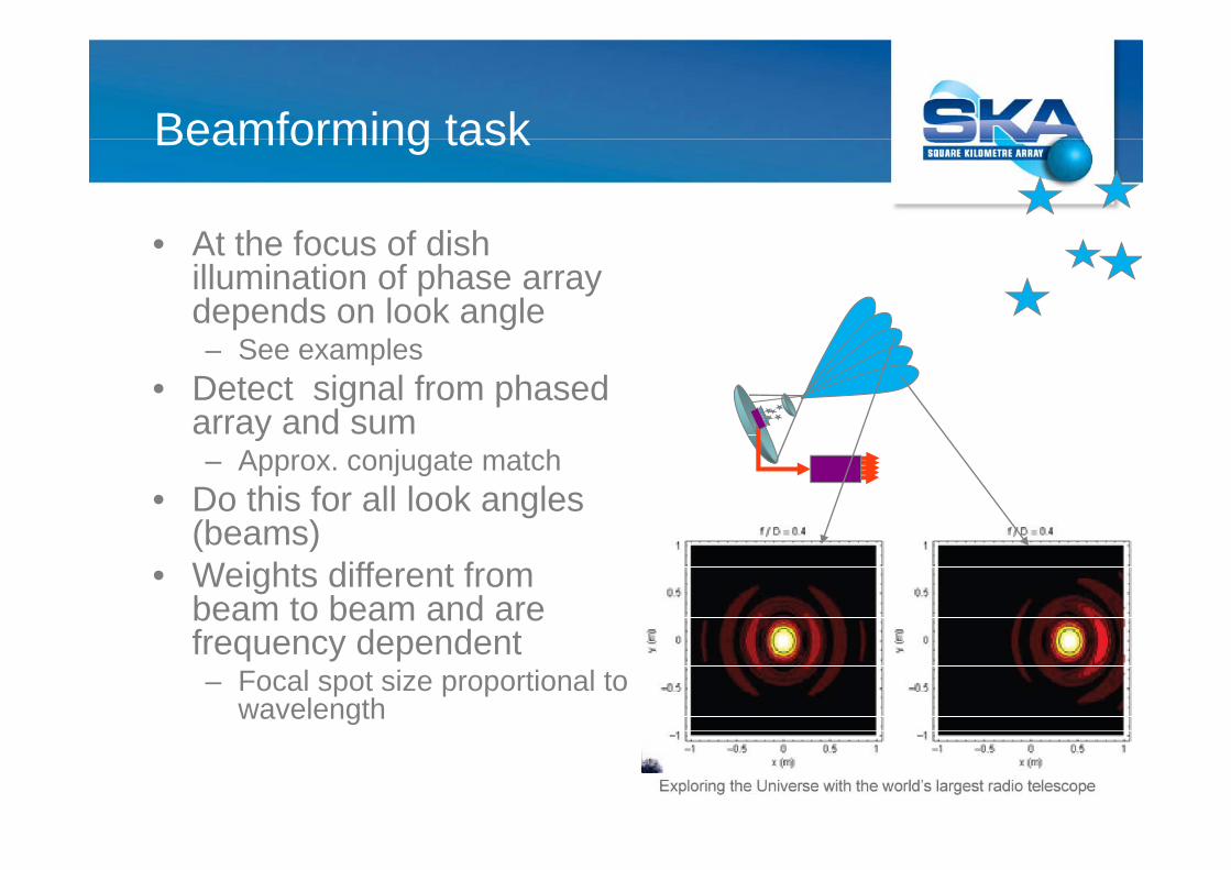
Beamforming taskBeamforming task
At the focus of dish• At the focus of dish illumination of phase array depends on look angle– See examples
• Detect signal from phased array and sumy– Approx. conjugate match
• Do this for all look angles (beams)(beams)
• Weights different from beam to beam and are f d d tfrequency dependent– Focal spot size proportional to
wavelength
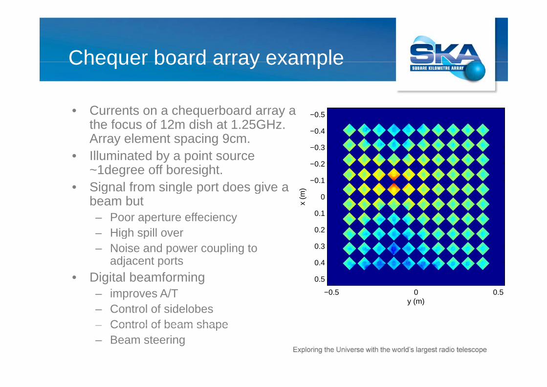
Chequer board array exampleChequer board array example
C t h b d t• Currents on a chequerboard array at the focus of 12m dish at 1.25GHz. Array element spacing 9cm.
−0.5
−0.4
−0.3• Illuminated by a point source
~1degree off boresight.• Signal from single port does give a
(m)
−0.3
−0.2
−0.1
0g g p g
beam but– Poor aperture effeciency– High spill over
x (m 0
0.1
0.2g p– Noise and power coupling to
adjacent ports• Digital beamforming
0.3
0.4
0.5Digital beamforming– improves A/T – Control of sidelobes– Control of beam shape
y (m)−0.5 0 0.5
0.5
– Control of beam shape– Beam steering

Time Domain BeamformingTime Domain Beamforming
B i ht d f ll l t ( )• Beam weighted sum of all elements (some zero)• Weighting is frequency dependent = filter h(t)
ports allover
)()()(j
jj tvthtBeam
• Compute load proportional to– No beams B– No elements N– Bandwidth BW– No filter taps (>40) T
• Multiplies/s ~2.5 B.N.BW.T
Frequency Domain BeamformingFrequency Domain Beamforming
D i t d t i t f h l• Decimate data into frequency channels– Must do this for FX correlator in any case– Multiplies/s ~40 N.BW
• Single complex weight per frequencySingle complex weight per frequency channel– Beam forming ~5 B N BW Multiplies/s– Beam forming ~5 B.N.BW Multiplies/s
– No beams B– No elements N– Bandwidth BWa d d
ComparisonComparison
• Equality time and frequency compute load when2.5 B.N.BW.T = 40 N.BW+5 B.N.BW
No taps T = 16/B + 2 • No beams B is the order of 50-100 (single pol )• No beams B is the order of 50-100 (single pol.)
– 25-50 Dual polarisation beams
• Allowable no of taps for equal compute load is ~2, need more than 40need more than 40.
• Use Frequency Domain Beamforming
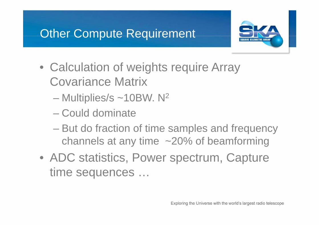
Other Compute RequirementOther Compute Requirement
• Calculation of weights require Array Covariance Matrix– Multiplies/s ~10BW. N2
Could dominate– Could dominate– But do fraction of time samples and frequency
h l t ti 20% f b f ichannels at any time ~20% of beamforming• ADC statistics, Power spectrum, Capture p p
time sequences …

Beamformer Architecture (Cross connect)
• For SKA Phase 1 probably have multiple beamformer boards
• Pass data through filterbank and distribute part of the bandwidth to each boardpart of the bandwidth to each board

Alternative Architecture (Ring)Alternative Architecture (Ring)
• Connect beamformer in ring• Same amount of input dataSame amount of input data• But data for all beams must be transported
b t b dbetween boards
• Use Cross Connect
Example – ASKAP ProcessingExample ASKAP Processing
• Note fine filterbank, coarse delay, transient buffer, fringe stopping considered part of correlator here
B f t t l itDi iti t t
ADCCoarse
Filterbank304 MHz out
ACM + Calibration
Correlations
Input
Beamformer at central siteDigitiser at antenna
ACM Data output
304 MHz out Correlations
Beamformer
All inputs
weights
Cross connect
1.9Tb/s Transient Buffer
Transient buffer output
Transient trigger
192 inputs
188 PAF elements3 Calibration1 RFI
Fine Filterbank
and coarse delay
gg
Fringe Stopping, fine delay & phase compensation
To Correlator
1 RFI
delayCoarse delay
compensation
Phase data

Data Transport form PAFData Transport form PAF
• Two options: Coaxial cable or Fibre• Coaxial cables expensive bulky and lossyCoaxial cables expensive, bulky and lossy
– Used in ASKAP and APERTIFT t i l t d l l– Transport signal to ground level
• Fibre is relatively cheap, low loss and easy y p, yto install– Until recently transmitters too expensive in– Until recently transmitters too expensive in
weight or $$. But this is changing.
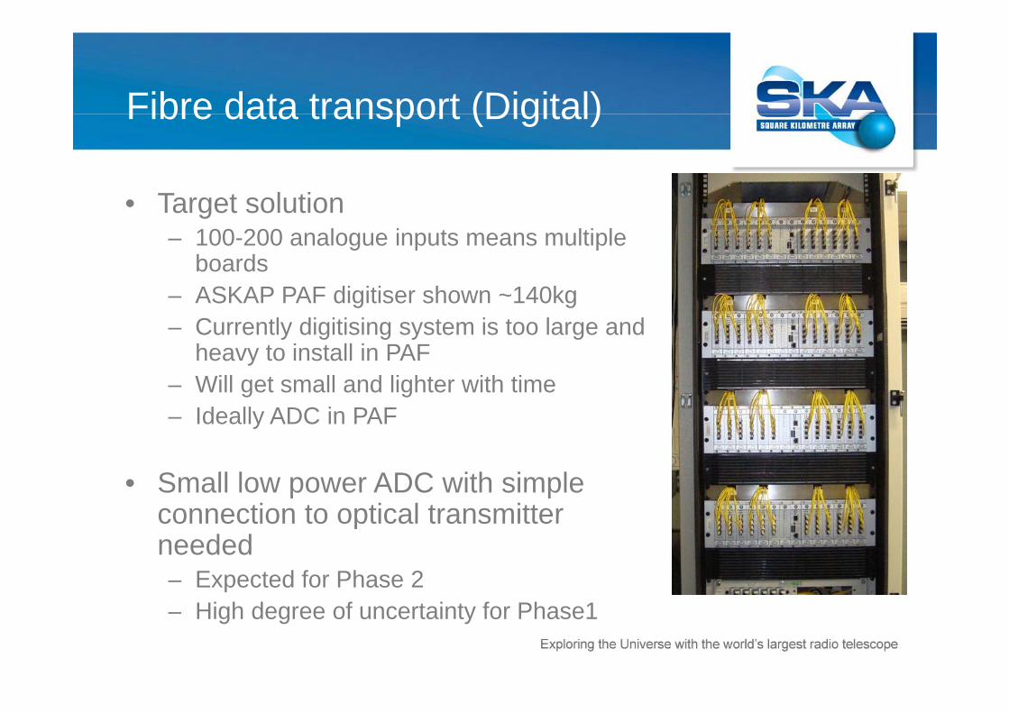
Fibre data transport (Digital)Fibre data transport (Digital)
T t l ti• Target solution– 100-200 analogue inputs means multiple
boards – ASKAP PAF digitiser shown ~140kg– Currently digitising system is too large and
heavy to install in PAFheavy to install in PAF– Will get small and lighter with time – Ideally ADC in PAF
• Small low power ADC with simple connection to optical transmitterconnection to optical transmitter needed– Expected for Phase 2– High degree of uncertainty for Phase1

Fibre data transport (RF over Fibre)Fibre data transport (RF over Fibre)
RF Fib h ll d t l• RF over Fibre has normally used external modulator
V d f– Very good performance – But cost is high
Directly modulate DFB laser have brought cost• Directly modulate DFB laser have brought cost down to reasonable values
Limitation high second order modulation– Limitation high second order modulation, • At most one octave bandwidth • Bandwidth similar to that of the proposed octave band feeds
– Small size and low power allows installation in PAF• Assume this is the solution used for
SKA Phase 1

Bandwidth and locationBandwidth and location
• RF over Fibre uses single mode fibre.– Transport for more than 10km (central site?)
• PAF say 1.5 – 0.6GHz need two octave bands – One is 1.2-0.6GHz – Some transition zone needed– assume correlator and beamformer 0.5GHz
bandwidth• Octave band direct sample in second Nyquist p yq
zone of ADC • Second band would be 1 5 to 1 0GHzSecond band would be 1.5 to 1.0GHz

Beamformer requirementsBeamformer requirements
• 500MHz bandwidth, 36 dual pol beams, 100 element per single pol beam
• Compute load– 500MHz x 72 single pol beams x100 complex g p p
MACs/beam x 4 multiplies/Complex MAC– 14.4T mult/sec plus over head ~20Tmult/s
• FPGA in 2016-17 has 8000 multipliers at 0.45GHz– 3.6T mults/s per FPGA - 6 FPGAs needed– Two boards to implement beamformer
• Smaller lower performance PAF – fewer FPGAsp

ADC/FilterbankADC/Filterbank
ADC t h 100 200 ti l RF i t• ADC system has 100-200 optical RF inputs.• Assume quad ADC = 25 to 50 ADCs
Say 5 Quad ADC per board– Say, 5 Quad ADC per board– 5 to 10 ADC boards
• Optical link to beamformer neededOptical link to beamformer needed – Use FPGA to packetise data and drive optical TX– Two links needed – one per beamformer boardp
• Use same FPGA for filterbank and each link carries data for half the bandwidth
• Filterbank for 1.6GHz sample rate ~32Gmultiplies/s
For 200 elements 6 4Tmuliplies/s = 10 small FPGAs– For 200 elements – 6.4Tmuliplies/s = 10 small FPGAs
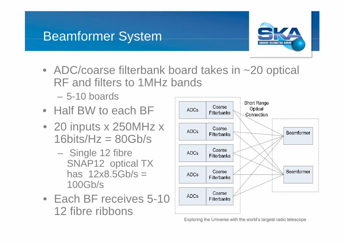
Beamformer SystemBeamformer System
ADC/ filt b k b d t k i 20 ti l• ADC/coarse filterbank board takes in ~20 optical RF and filters to 1MHz bands
5 10 b d– 5-10 boards• Half BW to each BF• 20 inputs x 250MHz x
16bits/Hz = 80Gb/sSi l 12 fib– Single 12 fibre SNAP12 optical TX has 12x8.5Gb/s =has 12x8.5Gb/s 100Gb/s
• Each BF receives 5-10 12 fibre ribbons
Data outputData output
• After beamforming pass data through filterbank to get final frequency resolutiong q y
• Quantise to 4+4bit resolution for correlator72 i l l b 500MH 8bit /H• 72 single pol beams x 500MHz x 8bits/Hz = 288Gb/s or 30x10G optical links for output data– 15 per board15 per board
Possible beamformer boardPossible beamformer board
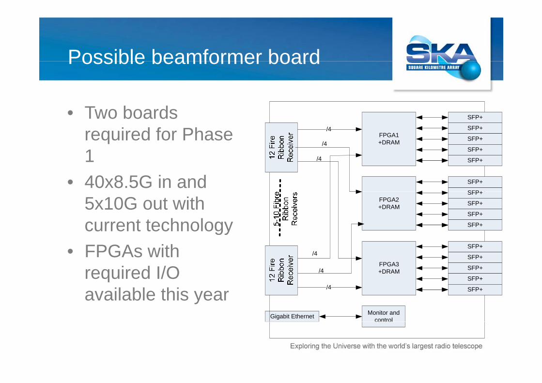
• Two boards required for Phase /4
FPGA1+DRAM/4
SFP+
SFP+
SFP+
SFP+
1• 40x8.5G in and
/4SFP+
SFP+
SFP+
SFP+
5x10G out with current technology
FPGA2+DRAM
SFP+
SFP+
SFP+
SFP+
• FPGAs with required I/O
FPGA3+DRAM/4
SFP+
SFP+
SFP+
/4SFP+
required I/O available this year
Monitor and controlGigabit Ethernet
/4SFP+
SFP+
co t o

Cost estimate Phase 1 (includes RF over Fibre)
A 8000 lti li FPGA $1k ADC• Assume 8000 multiplier FPGA ~$1k, ADC $40/input, RF over Fibre $100/linkC t f 200 l t PAF b f 54k€• Cost for 200 element PAF beamformer ~54k€
• 120 element PAF ~35k€ ($=0.75€)Beamformer component CostBeamformer boards and FPGAs $18,000ADC B f i l li k $4 000ADC-Beamformer optical links $4,000Coarse filterbank FPGA $2,500ADC $8,000
Estimate for 200 element PAF (10x10 dual pol)ADC $8,000
ADC / Coarse filterbank boards $10,000Transport of Analogue data to ADC $20,000
(10x10 dual pol)
Card cages, racks, power supplies $10,000
NRENRE
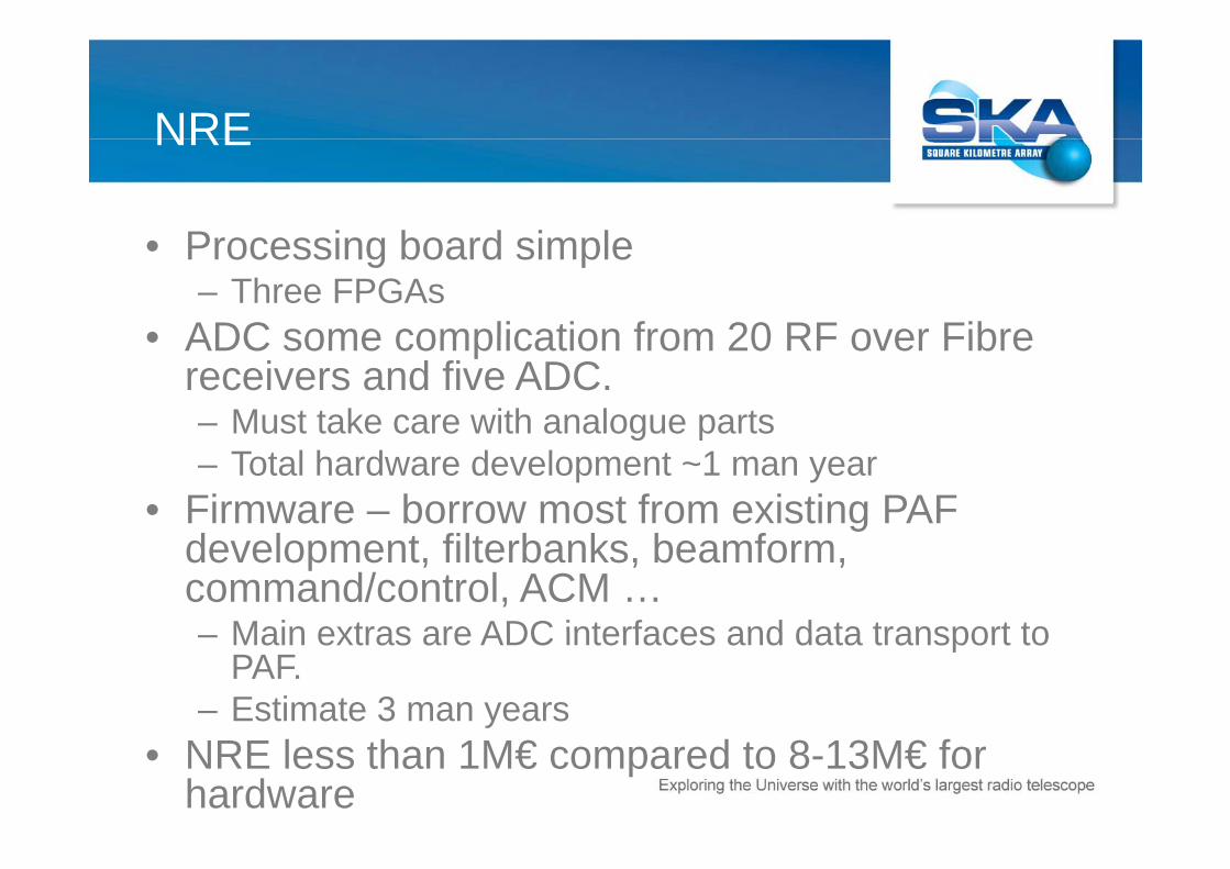
P i b d i l• Processing board simple– Three FPGAs
• ADC some complication from 20 RF over Fibre• ADC some complication from 20 RF over Fibre receivers and five ADC.– Must take care with analogue partsg p– Total hardware development ~1 man year
• Firmware – borrow most from existing PAF d l fil b k b fdevelopment, filterbanks, beamform, command/control, ACM …
Main extras are ADC interfaces and data transport to– Main extras are ADC interfaces and data transport to PAF.
– Estimate 3 man years• NRE less than 1M€ compared to 8-13M€ for
hardware

Coaxial Cable RevisitedCoaxial Cable Revisited
B f i 10 b d• Beamformer comprises ~10 boards.– Fits in a single chassis– But limited by need to attach 100-200 coaxial cables– But limited by need to attach 100-200 coaxial cables.
• Is small enough to mount on the dish, say under dish surface or on offset dish feed arm– Low cable loss, No coaxial cable through cable wraps
• Would allow wider bandwidth system but b bl iprobably no cost savings.
– Maintenance more difficultRFI shielding– RFI shielding
– Remote cooling– Need weather proof RF connectors and enclosure.Need weather proof RF connectors and enclosure.

SKA Phase 2 PAF BeamformerSKA Phase 2 PAF Beamformer
A ll l ADC d l d i• Assume small, low power ADC and laser driver developed. But must solve RFI problem for ADC in PAFin PAF
• Can now direct sample full RF 1.5-0.6 GHzADC 8 bit t 3 2 GS/ 25 6GS/• ADC 8-bits at 3.2 GS/s = 25.6GS/s
• Integrate 28Gb/s serialisers that directly drive l TXlaser TX.
• Target power 100-300mW per channel• Integrated on board with LNA or aggregate
many per board
Beamformer – Phase 2Beamformer Phase 2
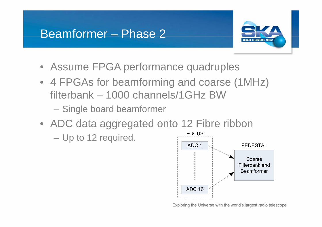
• Assume FPGA performance quadruples• 4 FPGAs for beamforming and coarse (1MHz) g ( )
filterbank – 1000 channels/1GHz BW– Single board beamformerg
• ADC data aggregated onto 12 Fibre ribbon– Up to 12 requiredUp to 12 required.

Costs Phase 2 BeamformerCosts Phase 2 Beamformer
$• Assume Quad ADC, without NRE, $32, FPGAs sill $1000, optical 12 channel TX $200.
• Total cost 15k€ for 200 elements
Beamformer component CostADC $1,600ADC-Beamformer digital optical $2.400ADC board and RFI enclosure x16 $3,200Processing board including FPGA $8 000Processing board including FPGA $8,000100 GE outputs x 8 $1,600“Pizza” box and power supplies $2,000p pp
ConclusionConclusion
Si l b d b f /filt b k b Ph 2• Single board beamformer/filterbank by Phase 2 • Digital electronics cost continue to decrease
COTS ADC and RF o er Fibre data transport• COTS ADC and RF over Fibre data transport major cost for Phase 1– Estimate beamformer cost 2015-17Estimate beamformer cost 2015 17– 200 element PAF ~54k€– 120 element PAF ~35k€
• For lowest cost Phase 2 need to develop integrated ADC the directly drives optical TX at
25Gb/s~25Gb/s – Cost for beamformer could be as low as ~15k€