pcb eda tutorial laboratory 3, design verification ... · cmpe174 lab-3, rev4.1.4 page 1 university...
TRANSCRIPT
Cmpe174 Lab-3, Rev4.1.4 page 1
University of California, Santa Cruz Computer Engineering Department
PCB EDA Tutorial Laboratory 3, Design Verification: Gerbtool 16.1
CMPE174, Intro to EDA Tools S.C. Petersen
1. INTRODUCTION AND OBJECTIVES Lab-2 ended with the manufacturing phase, where Gerber artwork and several drill files were created. This third laboratory continues where lab-2 ended, proceeding on with the Design Verification phase, where we now purposely inspect the these artwork and drill files that will eventually be sent on to a boardhouse. This phase is actually optional, but most layout engineers agree that being able to view standard format Gerber and drill files with a third-party “Gerber Viewer” is a good idea. The central objective is to use and appreciate the value of these free programs. Many of these programs have “full” versions capable of editing and regenerating exportable artwork and drill files.
2. GENERAL DISCUSSION The last step of the second phase disussed in lab-2 concentrated on preparing industry-standard files that would normally be sent on to a PCB manufacturing facility (aka “board house”). This end-phase of PCB design is really the most exacting, since everything basically must be “perfect”. The choice of board house largely determines which specific files must be created for final submission, typically via the Internet. Many board houses maintain FTP sites soley for this purpose. Beginners often fail to appreciate the fact that some hapless technician has to unpack your files, sans your understanding, and miraculously know exactly what you want made and proceed to manufacture the associated PCB. Hence, you should bear in mind that erring on the side of providing too much organizing information is better than too little. Indeed we followed this philosophy in lab-2 when creating content for APC’s wanted “mechanical” layer. When a board house can’t figure out what you want, or finds “errors” that were actually deliberate innovative features on your part, they will stop the process and contact you for clarification, typically costing at least one day’s delay. Gerbtool is a powerful computer-aided manufacturing tool (CAM) used by board houses and pcb designers alike. Why use GerbTool? After all, Allegro produces all the necessary Gerber and drill files anyway. So why not just use these? In fact, many engineers do just that – especially those inexperienced with PCB design. The answer has several aspects:
1. When working with a design in Allegro, the associated *.BRD file is not a Gerber formatted file. Hence, it behooves us to always view the generated artwork files with a program designed to input them to show us exactly what the board house will also see. Conversion to Gerber can sometimes result in strange errors that may require fixing back in Allegro. One common error is to get the drill and artwork files out of sync. This can happen if you make changes to the design where padstacks are moved, proceed to generate the artwork files, but fail to also export the accompanying drill files and instead continue to use an earlier, but now outdated, set of drill files. Generally, these errors are mostly caused by us – not the pcb tool.
2. Board houses often require special tooling marks be added to particular layers, or that specific information
be provided on new documentation layers. Also, mechanical information like cutting marks are typically more easily done with a CAM tool. Note that we included this in Lab-2, where you created a special Film layer: Mechanical, meant to address this requirement.
3. Tiling or “panelization” refers to the process of combining several PCB designs into a single large board.
The idea is to make a given PCB run more cost-effective. Then after getting the finished board back, the individual tiled boards are cut and separated from the single large parent board. This can be done with repeats of the same design, or may combine different designs. Although this can be done in Allegro by exporting and importing additional PCB designs as “modules”, any imported modules are made part of the
Cmpe174 Lab-3, Rev4.1.4 page 2
current design’s netlist that alters the reference designators on the SST and AST layers. Moreover, they also inherit current DRC and spacing constraint settings. Often, drills and other items get changed, causing problems unless they’re noted before sending off the Gerber files. Gerbtool, by constrast, only merges Gerber and drill files, so they are completely independent of netlist and spacing differences used to independently create them. This leads to better quality control overall and few side-effects.
4. Special viewing modes allow us to see the design in ways not possible in Allegro PCB. For example, using
“sketch mode” changes how draws and flashes are visually rendered to more accurately observe how they’re going to be made.
3. TUTORIAL PROJECT The tutorial project has already been discussed in the previous two labs, and won’t be repeated here. Refer to these labs for necessary background. As an exercise, we will review the necessary files required by Alberta Printed Circuits’ (APC) Basic Prototype and Plus Prototype services. Both of these services are meant for short-run engineering prototypes designed to rapidly turn-around 2-layer 62.5mil FR4 printed circuit boards. Basic Prototype runs require only top and bottom layer Gerber files, along with an aperture and two drill files (RS274X preferred; RS273D accepted). Plus Prototype is an enhanced more expensive service that allows boards to have green solder masking on both sides and optional silk-screening on the top layer or top and bottom layers . You can read about this board house at http://www.apcircuits.com/ . Before You Begin. You should have already created the following set of directories, those shown in black, in your student account. I include them here as a convenient reference and reminder of their relevance. …Tutorial - Top-level directory. Appnotes - Relevant application notes, industrial papers and references. Components - Mechanical footprint drawings, vender part references, bom’s etc. Datasheets - Technical datasheets for all devices used in this project. Handset - Tutorial project folder containing schematics and pcb layout files. v1.0 Handset(APC Basic Prototype) - see discussion below v1.0 Handset(APC Plus Prototype) - see discussion below. pcb - Board-level PCB files and colorviews. artwork - Exportable Gerber and drill files. logs - Stuff Allegro produces. reports - More stuff Allegro produces. Lib - Capture schematic symbols (*.olb files) and related pcb footprint libraries. local - Local configuration files. modules - Module files. parameter - Parameter files (*.prm). tech - Technology constraint files (*.tcf). templates - Empty “template” board files (*.brd). padstacks - PCB surface-mount pads and through-hole definitions; used with footprints. symbols - footprints: (*.dra), padstacks (*.pad) and various compiled symbol files (*.*sm). Do not proceed to start working with Gerbtool unless the following has already been done:
• The board design started in Allegro PCB is finished, leading to a created a final PCB resolving all DRC warnings and errors.
• The manufacturing phase is complete, and all necessary RS-274X formatted Gerber and drill files have
been created.
Create two additional directories in your Handset folder, and call one v1.0 Handset(APC Basic Prototype) and the second, v1.0 Handset(APC Plus Prototype). We will use these folders only for files and other documentation

Cmpe174 Lab-3, Rev4.1.4 page 3
directly related to APC’s two standard prototyping services. You can navigate now to http://www.apcircuits.com/ and learn about these two services. This laboratory shows you how to create the necessary files for each type. If you haven’t read it yet, read the rs274xrevd_e.pdf industrial reference paper that should already be in your AppNotes folder. If it isn’t, download it from our website now under the Tutorial project folder (its in the App Notes folder) and place it in your working AppNotes project folder. This short paper, titled , “Gerber RS-274 Format, User’s Guide” has a good introduction and discussion of the Gerber format. You should be able to discuss the major differences between RS274D and RS274X standards.
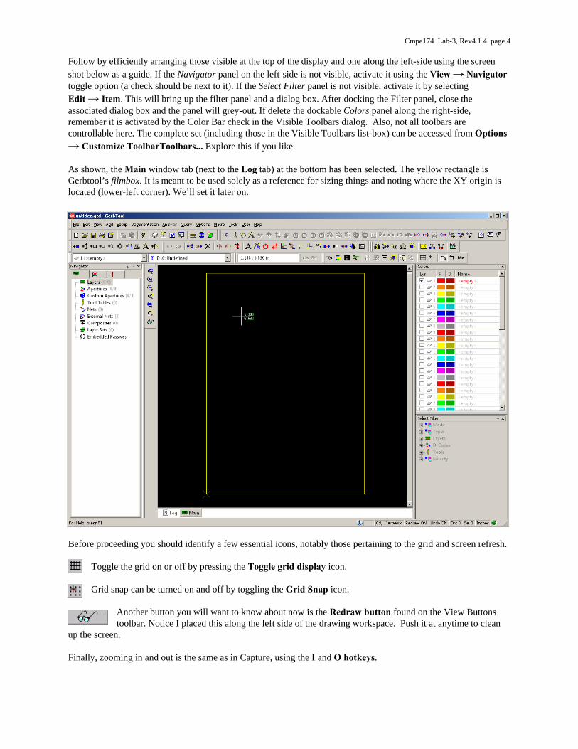
4.0 Using GerbTool GETTING STARTED – Begin by launching Gerbtool from the Start Menu or desktop icon (if present). This tool has many toolbars, and they are all dockable. When all are visible, they take up considerable space at the top of the program’s GUI. Moreover, the default screen locations are poorly placed – tending to just be stacked one on top of another. Hence, we will turn some of them off and re-arrange the rest. I’ve moved all the default groupings onto the desktop and snapped a screen shot so you can identify them. Note too that some of these icons have no equivalent hotkeys or menu selections.
Visibility is controlled by group, by choosing View Toolbars... to bring up the Visible Toolbars listbox shown (left and right cover all choices since the box is not sizable). Set visibility as shown and press OK.
Cmpe174 Lab-3, Rev4.1.4 page 4
Follow by efficiently arranging those visible at the top of the display and one along the left-side using the screen shot below as a guide. If the Navigator panel on the left-side is not visible, activate it using the View → Navigator toggle option (a check should be next to it). If the Select Filter panel is not visible, activate it by selecting Edit → Item. This will bring up the filter panel and a dialog box. After docking the Filter panel, close the associated dialog box and the panel will grey-out. If delete the dockable Colors panel along the right-side, remember it is activated by the Color Bar check in the Visible Toolbars dialog. Also, not all toolbars are controllable here. The complete set (including those in the Visible Toolbars list-box) can be accessed from Options → Customize ToolbarToolbars... Explore this if you like. As shown, the Main window tab (next to the Log tab) at the bottom has been selected. The yellow rectangle is Gerbtool’s filmbox. It is meant to be used solely as a reference for sizing things and noting where the XY origin is located (lower-left corner). We’ll set it later on.
Before proceeding you should identify a few essential icons, notably those pertaining to the grid and screen refresh.
Toggle the grid on or off by pressing the Toggle grid display icon. Grid snap can be turned on and off by toggling the Grid Snap icon.
Another button you will want to know about now is the Redraw button found on the View Buttons toolbar. Notice I placed this along the left side of the drawing workspace. Push it at anytime to clean
up the screen. Finally, zooming in and out is the same as in Capture, using the I and O hotkeys.

Cmpe174 Lab-3, Rev4.1.4 page 5
4.1 SETTING GERBTOOL PARAMETERS GerbTool’s default settings are usually not what we want to work with,so let’s set and define the important ones now. Select menu sequence Options → Configure… to bring up the tabbed Configuration dialog, and select tab Units and Precision and set the precision to a more realistic of 0.001 inch (1/1000). Select the Display tab and change the film box to something you can actually see on the screen; note this can be changed anytime you like.
Unlike Allegro, GerbTool has only one grid. Leave it set for 100 mils as shown. Click OK and close the dialog. IMPORTING DESIGN FILES – Gerbtool is capable of importing designs created by many different EDA tools. The screen shot below shows the options associated with the import function. Selections from Barco on down (excluding Netlist) are various common formats. We will only look at the top two sets:
Import Wizard… is an intelligent interface that can automate the importation process, but should only be used by those with experience. Gerber… allows us to manually browse and select one or more Gerber formatted files. Aperture List… allows us to manually browse and select single aperture files. These map light pen sizes (apertures) and shapes as specific “D-Codes” referenced in associated RS274D Gerber files. Artwork generated using RS274X already have this aperture information included in the Gerber files themselves, so this file is not needed. NC (Drill/Mill)…allows us to manually browse for one of the two necessary drill files having the NC (numerically controlled) XY drill location information. Each drill size is mapped to a tool or “T-Code” that actually species the drill used. NC Tool List… allows us to manually browse for the second necessary drill file noted above.
We will use the easier manual approach. After you get some skill distinguishing filetypes and their functions, the wizard is faster.

Cmpe174 Lab-3, Rev4.1.4 page 6
Let’s begin by first importing the RS274X Gerber files you created at the end of lab-2. Select the Gerber option and navigate to your …Handset\pcb\artwork folder. An example is shown following:
You should recognize these as various artwork files generated by Allegro. Other files exist in this folder, but are masked to clearly identify only those that Gerbtool associates with particular file extensions. The Cadence Allegro *.art extension is one of the extensions that Gerbtool knows about when first installed. This list is configurable by accessing the Configuration panel noted on page 5.
Select all the Gerber files shown above and press the Open button. The Gerber Import Data Format dialog will appear for the first Gerber file in the list, in this case it’s for the bottom layer. Options here apply to the entire set of files selected. Notice that Gerbtool has properly identified the “Dialect” as RS274X. The “m.n” precision also agrees with what you set back in the manufacturing phase of Allegro. If any of these were wrong, they could be corrected here. Press OK. Gerbtool should proceed to process each file assigning them to empty layers successively in the Colors panel. Entries will be made in the Log and can be inspected by selecting the Log tab at the bottom of the page. Warnings and errors will appear here. Note: if you encounter one or more warnings stating that undefined or zero size apertures were found in particular files, it will most likely be on the Mechanical layer, where the drill chart figure symbols didn’t get mapped properly back in Allegro. Although I’ll tell you how to fix this, you should continue on to see the effect it has. Most likely the drill table and drill symbols appear as dots. To correct this, specify in Allegro during the manufacturing step on the Artwork Control Form (comes up when you choose menu sequence Manufacture → Artwork ) that any undefined line widths be given a non-zero value. Therefore, simply set the Undefined line width: field to 1.0 and re-create the Gerber files.

Cmpe174 Lab-3, Rev4.1.4 page 7
As shown above, GerbTool loaded the 7 Gerber files created by Allegro and shows them all by default. I removed the board outline from the Mechanical layer and re-generated the artwork, leaving only the cut-marks since the board house doesn’t really need it and it only obscures where the actual corners are; do you see why? In Allegro, the two sub-classes were differently colored. Here, they’re the same – and the board house will see it the way Gerbtool does. The far-right tool bar controls layer visibility and color. The default colors are pretty weird, so I set each one by double-clicking on each color rectangle. The two colors associated with each layer are used to distinguish between draws and flashes, where the left color is for flashes (“F”) and the right for draws (“D”). Colors may be changed at any time simply by clicking any of the colored squares and selecting a new color. Layers have their corresponding visibility checkboxes checked. Hence,
layers 1 through 7 are visible. Right-clicking after selecting a layer brings up three menu options for setting it active or toggling all layers on off; this is shown for the third layer. Try this now. Set all your colors and toggle various layers on and off. You may have noticed the icons for each layer are different than the default oblique green rectangles. These specify what a layer’s basic type is. If you later merge other boards to your design, make sure these layer types agree. Defined them by going over to the Navigator panel, expanding the virtual Layers folder and selecting any of the 7 layers and right-clicking to bring up

Cmpe174 Lab-3, Rev4.1.4 page 8
the menu shown at left. Selecting the Spreadsheet option will then access the wanted Layer Setup spreadsheet shown on the next page.
Tip: When tiling different boards together to make a single large board to be sent off to a board house, be sure the layer types all agree; they should each be of type “other” if undefined, or specifically set to one the types noted below.
This dialog provides all the features the Colors panel omits. I’ve selected a particular layer in the Type column to access various standard layer definitions. Colors and layer names can also be edited here. Go ahead and define your layer types now and press OK.
WORKING WITH OBJECTS – Gerbtool allows us to select objects on any layer or group of layers for such actions as deleting, moving, copying etc. The versatility is very sophisticated and extends beyond what Allegro is capable of. I will illustrate this by moving the entire design to align with the film box origin at XY = [0,0].
If the Units and Precision were correctly set to “Inches” and “1/1000…” earlier (see page 5), then the cursor cross-hair should be showing three decimal points. Moreover, the pcb layout is probably outside the 5.000 X 7.000 inch film box as shown in the screen shot. The objective is to select everything on all 7 layers and move them so the lower-left cut mark is precisely aligned with the film box’s lower left reference corner at the coordinate origin.
To move everything, first make sure all layers are visible, then turn the grid on and using either the icon shown , or the Edit → Move menu sequence, activate the move function. When this happens, notice the
Cmpe174 Lab-3, Rev4.1.4 page 9
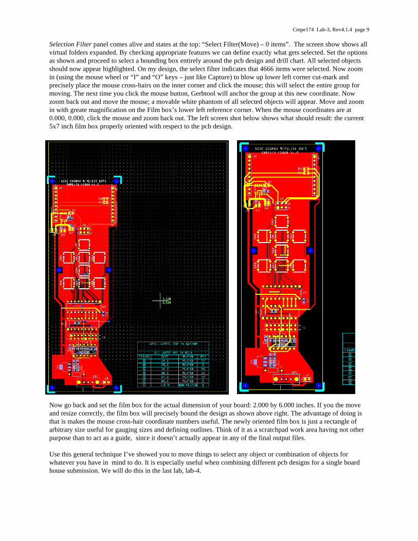
Selection Filter panel comes alive and states at the top: “Select Filter(Move) – 0 items”. The screen show shows all virtual folders expanded. By checking appropriate features we can define exactly what gets selected. Set the options as shown and proceed to select a bounding box entirely around the pcb design and drill chart. All selected objects should now appear highlighted. On my design, the select filter indicates that 4666 items were selected. Now zoom in (using the mouse wheel or “I” and “O” keys – just like Capture) to blow up lower left corner cut-mark and precisely place the mouse cross-hairs on the inner corner and click the mouse; this will select the entire group for moving. The next time you click the mouse button, Gerbtool will anchor the group at this new coordinate. Now zoom back out and move the mouse; a movable white phantom of all selected objects will appear. Move and zoom in with greate magnification on the Film box’s lower left reference corner. When the mouse coordinates are at 0.000, 0.000, click the mouse and zoom back out. The left screen shot below shows what should result: the current 5x7 inch film box properly oriented with respect to the pcb design.
Now go back and set the film box for the actual dimension of your board: 2.000 by 6.000 inches. If you the move and resize correctly, the film box will precisely bound the design as shown above right. The advantage of doing is that is makes the mouse cross-hair coordinate numbers useful. The newly oriented film box is just a rectangle of arbitrary size useful for gauging sizes and defining outlines. Think of it as a scratchpad work area having not other purpose than to act as a guide, since it doesn’t actually appear in any of the final output files. Use this general technique I’ve showed you to move things to select any object or combination of objects for whatever you have in mind to do. It is especially useful when combining different pcb designs for a single board house submission. We will do this in the last lab, lab-4.

Cmpe174 Lab-3, Rev4.1.4 page 10
DRAWS AND FLASHES – Now turn off all but the top layer. Notice the flashes and draws are both the same color. If you wanted to distinguish them, change their colors. The side-by-side comparison show the effects of this:
Both flashes and draws are the same color.
Flashes are green and draws are yellow.
Remember, a “flash” is a light-pen having some aperture shape, round, rectangular, square etc. that is precisely positioned and “flashed” – much like a strobe light is – to define pads for vias and surface mount parts. A “draw” is a light-pen whose aperture is used to define traces – and hence requires moving the pen. This should be evident in the side-by-side comparison above. I like to make the flashes and draws different shades of the same color to keep them clearly associated with the same layer. It isn’t essential to distinguish flashes and draws, but it can be very useful when verifying drills, since every drill will include a flash (assuming a copper pad is involved); SM (surface-mount) pads will also be flashes, but won’t have drills through them. Take some time now and experiment with the layers toolbar. Identify the various layers, turning them on alone, changing their colors to distinguish draws and flashes, etc.
Cmpe174 Lab-3, Rev4.1.4 page 11
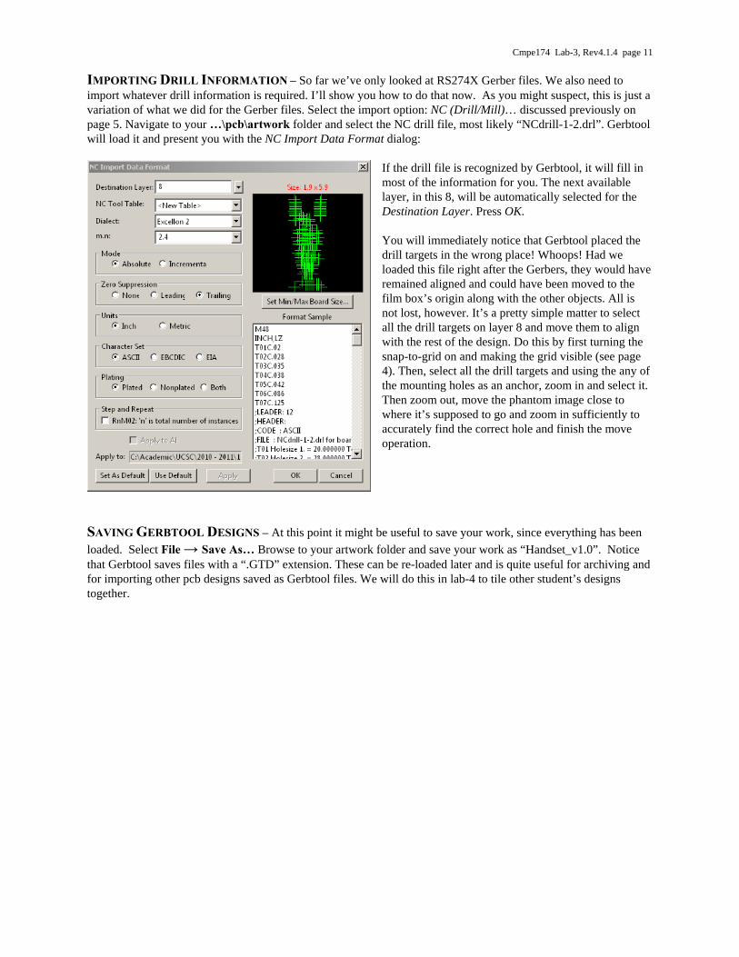
IMPORTING DRILL INFORMATION – So far we’ve only looked at RS274X Gerber files. We also need to import whatever drill information is required. I’ll show you how to do that now. As you might suspect, this is just a variation of what we did for the Gerber files. Select the import option: NC (Drill/Mill)… discussed previously on page 5. Navigate to your …\pcb\artwork folder and select the NC drill file, most likely “NCdrill-1-2.drl”. Gerbtool will load it and present you with the NC Import Data Format dialog:
If the drill file is recognized by Gerbtool, it will fill in most of the information for you. The next available layer, in this 8, will be automatically selected for the Destination Layer. Press OK. You will immediately notice that Gerbtool placed the drill targets in the wrong place! Whoops! Had we loaded this file right after the Gerbers, they would have remained aligned and could have been moved to the film box’s origin along with the other objects. All is not lost, however. It’s a pretty simple matter to select all the drill targets on layer 8 and move them to align with the rest of the design. Do this by first turning the snap-to-grid on and making the grid visible (see page 4). Then, select all the drill targets and using the any of the mounting holes as an anchor, zoom in and select it. Then zoom out, move the phantom image close to where it’s supposed to go and zoom in sufficiently to accurately find the correct hole and finish the move operation.
SAVING GERBTOOL DESIGNS – At this point it might be useful to save your work, since everything has been loaded. Select File → Save As… Browse to your artwork folder and save your work as “Handset_v1.0”. Notice that Gerbtool saves files with a “.GTD” extension. These can be re-loaded later and is quite useful for archiving and for importing other pcb designs saved as Gerbtool files. We will do this in lab-4 to tile other student’s designs together.

Cmpe174 Lab-3, Rev4.1.4 page 12
4.2 CHECKING YOUR DESIGN Since GerbTool sees what the board house does, verify each layer looks as it should with respect to clearances, trace width, lettering etc. Do this now for the Top copper layer. After that carefully inspect the copper pour on the bottom layer. In particular, check any spacings that appear to be too close.
Measure distances using the Measurement Tool; be sure the snap to grid is off. The tool works by anchoring a beginning point with the left mouse button and dragging a white vector line anywhere on the display. GerbTool will continually report on the absolute X-Y position as well as the distance in the lower left corner of the screen. Your current design shouldn’t have any clearance problems if you paid attention to the DRC back in Layout. The example shows the very enlarged clearance between a via pad on the bottom layer and the surrounding copper pour. We see this is 8 mils, which agrees with this dynamic shape’s setting when we created it in Layout. Although these may seem to be unnecessary and redundant, they will reveal errors made back in Allegro… Ones that we, perhaps, thought differently about then.
SPECIAL VIEWING MODES – Gerbtool has several very useful viewing modes not available in Allegro PCB that are very useful. These can be accessed from the Setting Buttons toolbar shown. I will show you the first two of these: Toggle Sketch Mode and
“This command toggles overlay mode on/off. When overlay mode is enabled, items on layers become transparent when drawn over those other layers. When overlay mode is disabled, items on layers obscure whatever is drawn underneath them. Overlay mode makes it easier to spot stacked and buried items. Flashes also display significantly faster in overlay mode.”

Cmpe174 Lab-3, Rev4.1.4 page 13
QUERYING DRILLS AND D-CODES – Determine what D-code an object is associated and object by selecting menu sequence Query → Item (or use the icon). This will display the Items Properties. The screen shot on the left below shows the result after selecting the square pad at in the upper left corner (the top layer was made active and the only one visible). The item is a square 62 mil flash aperture with D-Code D99. Try selecting
traces and pads to observe their properties. You will notice that all traces are draws and pads are flashes.
For the screen shot on the right, I made the drill layer active and the only one visible. I also got rid of the cross-hairs by unchecking the Display cross-hair at each drill hit option on the NC Settings panel in the Configuration set of panels (see pg. 5 for accessing these panels). For greater clariy, I also changed the color to yellow. Selecting the same square pad, GerbTool responds by telling us this is a 42 mil drill mapped to tool #5. Click on other objects and check their sizes as well. Note that even though the selection filter is set to query objects other than flashes, we could uncheck these, but it wouldn’t matter, since only flashes are present on this layer anyway. If you’re wondering what Arc’s and Poly’s are, they’re another variety of D-code used not used in our design (and only part of RS274X).

Cmpe174 Lab-3, Rev4.1.4 page 14
4.3 EXPORTING A DESIGN FOR BASIC PROTYPING So long as you are working only with a single pcb, the following steps aren’t really necessary, since the Gerber and drill files created by Allegro are sufficient to send off to the board house. Ther are only really necessary when we want to merge several pcb designs, as you will be doing in lab-4. Hence, knowing how to export directly from Gerbtool is sufficient for single or merged pcb designs. When merging or tiling different designs, it’s easiest to first create separated Gerbtool *.GTD files and them merge these. Again, you will do this in the next lab. For now, I’ll just review the export phase of the general process. APC’s Basic service results in a 2-sided pcb having only plated copper on the top and bottom sides of the board, while the second adds solder-mask and silk-screen (aka “legends”) options. To get a better idea of these two services and how they’re priced, got to their website now at http://www.apcircuits.com/ and read about these two services . You should also peruse their “Job Estimator” to get a better idea of how these options affect pricing. Note that APC tells us that “Basic orders approved by our cam department before 1PM Eastern ship the next business day!”. CREATING DRILL FILES – Generally, Gerbtool is capable of creating NC drill layers directly from Gerber files and Gerber layers from NC drill layers. Sometimes this is necessary, especially when combining designs having different drill sizes and layers. This will be explored in the next lab if it is needed.
If the drill layer looks good, optimize it by selecting the Optimize NC Layer icon.
This will bring up the Optimize NC Layer dialog. Make sure the NC layer is 8 and press OK. This will optimize the order the drill tools are selected and drilled on the PCB. We are now ready to create the two standard drill files, one having the NC X-Y coordinates for each drilled hole, and the other a list of tool numbers associated with each drill size.
Generate the tool list file by following menu sequence File → Export → NC Tool List…
or by using the NC Tool Report icon shown.
The NC Usage Report spreadsheet will appear. Check it for accuracy and the Press Save…. Navigate to the v1.0 Handset(APC Basic Prototype) folder and name the file: Handset.rpt
Cmpe174 Lab-3, Rev4.1.4 page 15
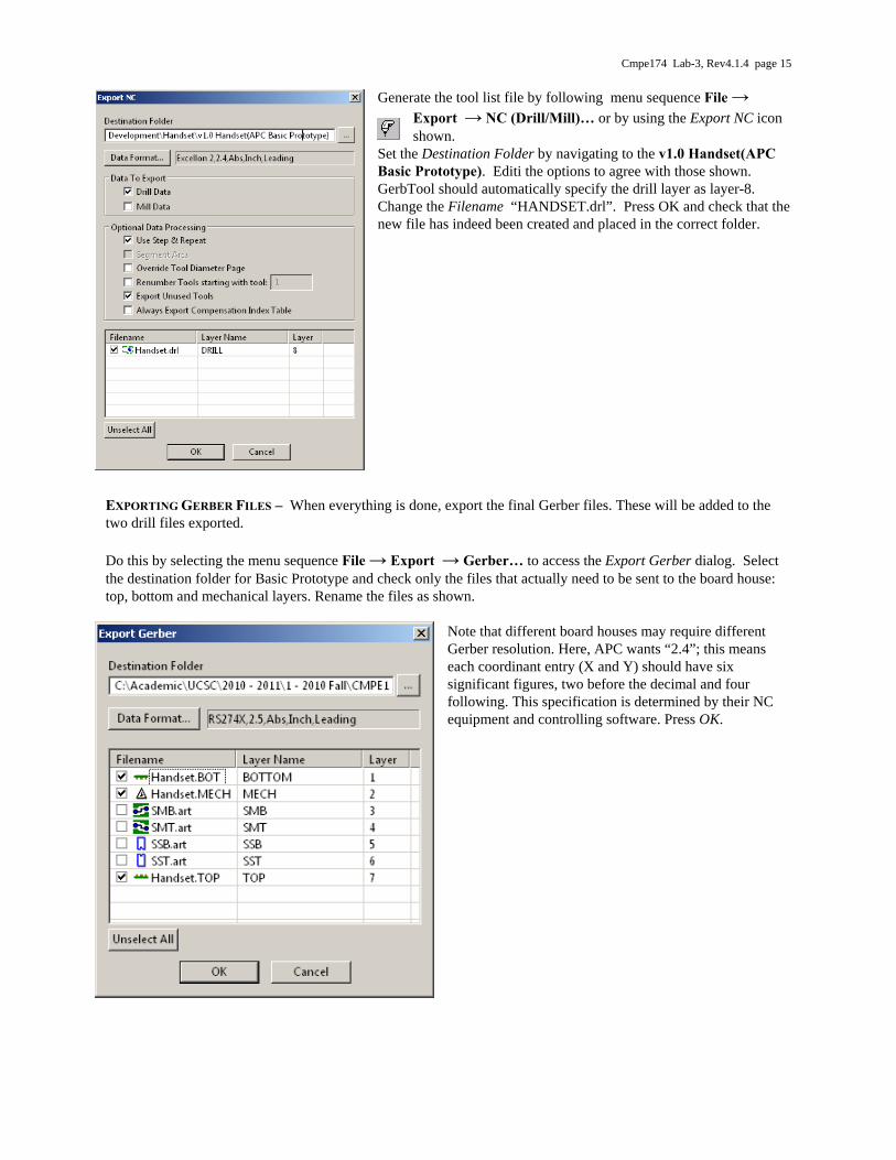
Generate the tool list file by following menu sequence File → Export → NC (Drill/Mill)… or by using the Export NC icon shown.
Set the Destination Folder by navigating to the v1.0 Handset(APC Basic Prototype). Editi the options to agree with those shown. GerbTool should automatically specify the drill layer as layer-8. Change the Filename “HANDSET.drl”. Press OK and check that the new file has indeed been created and placed in the correct folder.
EXPORTING GERBER FILES – When everything is done, export the final Gerber files. These will be added to the two drill files exported. Do this by selecting the menu sequence File → Export → Gerber… to access the Export Gerber dialog. Select the destination folder for Basic Prototype and check only the files that actually need to be sent to the board house: top, bottom and mechanical layers. Rename the files as shown.
Note that different board houses may require different Gerber resolution. Here, APC wants “2.4”; this means each coordinant entry (X and Y) should have six significant figures, two before the decimal and four following. This specification is determined by their NC equipment and controlling software. Press OK.

Cmpe174 Lab-3, Rev4.1.4 page 16
4.4 EXPORTING YOUR DESIGN FOR PLUS PROTYPING APC’s Plus Protyping is an enhanced service that allows us to add solder-mask on both the top and bottom sides of our pcb, and optionally add silk-screen (aka “legends”) on either or both sides. Navigate now to http://www.apcircuits.com/ and read about this service . Peruse their “Job Estimator” to get a better idea of how these options affect pricing. Because this service requires more steps than Basic Prototyping, APC carefully states that “Plus orders approved by our cam department before 9AM Eastern may ship as early as the next business day!” (italics mine). Whereas the basic service always ships the following day, this isn’t necessarily true for the plus service (italics mine). In my experience, the latter always ships at least one day later than the former. The necessary files for Plus Prototype are:
1. HANDSET.TOP (top or “component-side” copper layer [Gerber]) 2. HANDSET.SMT (solder mask top [Gerber]) 3. HANDSET.SST (only if top legend is selected [Gerber]) 4. HANDSET.BOT (bottom or “solder-side” copper layer [Gerber]) 5. HANDSET.SMB (solder mask bottom [Gerber]) 6. HANDSET.SSB (only if bottom legend is selected [Gerber]) 7. HANDSET.drl (NC drill tool list) 8. HANDSET.rpt (mechanical layer with board outline online and identifying text)
When you export the Gerber files noted, be sure they are type RS274X. Otherwise everything else is basically done the same as for the Basic service. 4.5 SUBMITTING YOUR DESIGN TO THE BOARDHOUSE You should thoroughly understand what a particular board house wants submitted. Most have some kind of “order form” that summarizes everything related to a particular order. Since this lab exercise uses Alberta Printed Circuits, you should navigate to their website now and review what needs to be sent to them for both the Basic and Plus services. Begin by selecting the “Sending Data” link on their menu bar. This will bring up their “How to Order” information screen. Recently, they added a Windows program, APClient, written in Delphi that streamlines specifying and submitting all necessary files; it’s quite worth the time to download and review it. Alternatively, you can always use their ascii-based order form. Just follow the “required files” link and then select the “order form” field. For this assignment, fill out the orderform.txt and show it as evidence you have reviewed the website and understand how what needs to be submitted to APCircuits; fill out two forms: one for Basic and the second for Plus.

Cmpe174 Lab-3, Rev4.1.4 page 17
5. CONCLUSION This concludes the design verification laboratory. This lab gave a good introduction to the files necessary to make PCB’s: Gerber and drill files. Gerbtool has many more features than were covered in this lab. You will see some of these features used in lab-4. Moreover, RS-274X has some sophisticated enhancements added to the older classical RS-274D format, such as polygons and macros. Some of these were used to implement the copper pours and areas used in your design. Oral Evaluation of your work for grading: Your grade for this laboratory will be based on showing the instructor compentence using GC Prevue and understanding things presented and discussed in the lab. Your understanding will be gauged by responses to any of the following topics and questions.You will be asked to answer or expound on several of them. Your grade for this laboratory will be based on showing the instructor compentence using Gerbtoolut tool and understanding things presented and discussed in the lab. Your understanding will be gauged by responses to any of the following topics. You will be asked to answer or expound on several of them.
1. Why use Gerbtool? 2. What are Gerber files? 3. What is the purpose of the “Mechanical” Layer. 4. Why doesn’t Gerbtool have a DRC feature like Layout does? 5. The film box. 6. Use of the grid in Gerbtool. 7. Explain the difference between “draw” and “flash” D-codes. 8. What are D-codes anyway? 9. What’s an aperture file? 10. Explain what happens when you convert “Gerber to Drill” and why it’s necessary. 11. Compare and constrast RS274X and RS274D export standards. 12. What are the capabilities of RS274X over RS274D? 13. Explain the role of Gerber and drill files in the manufacturing process. 14. Discuss the contents of RS274D and RS274X formatted files. 15. Discuss the contents of the NC drill file. 16. Discuss the contents of the drill tool file (aka “the drill rack”). 17. How are the NC drill and tool files related?