photovoltaics - the power of choice · pdf filephotovoltaics the power of choice the national...
TRANSCRIPT

P H O T O V O LTA I C St h e p o w e r o f c h o i c e
T H E N AT I O N A L P H O T O V O LTA I C S P R O G R A M P L A N F O R 1 9 9 6 – 2 0 0 0

Our Mission . . . . . . . . . . . . . . . . . . . . . . . . . . . . . . . . . . 1
Executive Summary . . . . . . . . . . . . . . . . . . . . . . . . . . . 2The PV Promise . . . . . . . . . . . . . . . . . . . . . . . . . . . . 3The PV Challenge . . . . . . . . . . . . . . . . . . . . . . . . . . 4Meeting the Challenge . . . . . . . . . . . . . . . . . . . . . . . 4Implementing the Program . . . . . . . . . . . . . . . . . . . . 6Guiding the Effort . . . . . . . . . . . . . . . . . . . . . . . . . . . 9
The PV Promise . . . . . . . . . . . . . . . . . . . . . . . . . . . . . 10
The PV Challenge . . . . . . . . . . . . . . . . . . . . . . . . . . . . 12
Meeting the Challenge . . . . . . . . . . . . . . . . . . . . . . . . . 14The Laboratories . . . . . . . . . . . . . . . . . . . . . . . . . . . 16Universities . . . . . . . . . . . . . . . . . . . . . . . . . . . . . . . 16
Industry . . . . . . . . . . . . . . . . . . . . . . . . . . . . . . . . . . 16Program Goals . . . . . . . . . . . . . . . . . . . . . . . . . . . . . 17
Implementing the Program . . . . . . . . . . . . . . . . . . . . . . 18Research and Development . . . . . . . . . . . . . . . . . . . 20Technology Development . . . . . . . . . . . . . . . . . . . . . 24Systems Engineering and Applications . . . . . . . . . . 26
Guiding the Effort . . . . . . . . . . . . . . . . . . . . . . . . . . . . 28Establishing Policies . . . . . . . . . . . . . . . . . . . . . . . . 29Organizing the National Program . . . . . . . . . . . . . . . 29Setting Strategies and Schedules . . . . . . . . . . . . . . . 30Funding the Program . . . . . . . . . . . . . . . . . . . . . . . . 30
PV Program TechnicalAreas and Milestones . . . . . . . . . . . Inside Back Cover
Contents
i

Our mission is to make photovoltaics (PV) a significantpart of the domestic economy—as an industry and an ener-gy resource. More than two decades of research and devel-opment (R&D), in partnership with industry, has advancedPV from a laboratory novelty to today’s growing U.S. indus-try, which grossed more than $350 million in 1995.
With further R&D, photovoltaics will contribute muchmore to the national economy. Reducing system costs fromabout $7 per watt to $3 per watt could result in a domesticindustry with billions of dollars in annual sales. A recentmarket study by the Utility PhotoVoltaic Group estimated apotential domestic market for PV of 9000 megawatts at asystem price of $3 per watt. Photovoltaics has enormouspotential as a cost-competitive source of electricity becausereducing costs to below $3 per watt is also possible.
We face a number of challenges to reduce the cost ofelectricity generated by PV systems and to increase theirefficiency and lifetime. Working together, researchers in thenational laboratories, the nation’s universities, andindustry—the three major participants in the NationalPhotovoltaics Program—are prepared to meet thesechallenges.
We will meet them with a well-balanced nationalprogram, with key milestones in both basic research andtechnology applications. The program includes world-classR&D to maintain U.S. leadership in technical breakthroughsand extensive work with industry to reduce manufacturingcosts and to improve systems. The program also includesprojects that validate today’s prototype systems inapplications throughout the world.
This 5-year plan for the National Photovoltaics Pro-gram outlines initiatives such as the Thin-Film PV Partner-ship, new phases of the PV Manufacturing Technology(PVMaT) Program, and Utility PhotoVoltaic Group projectsfor system validation. It also provides for cooperativeinternational activities with the World Bank, the GlobalEnvironmental Facility, and applications in Asia, South andCentral America, Africa, Eastern Europe, and the republicsof the former Soviet Union.
Our discussions with industry and utility leaders helpus recognize that, to make PV a significant part of oureconomy, we must develop technology for specificapplications. As PV system costs decline, the range ofsystem uses will expand from today’s high-value consumerproducts and remote applications to grid-connected buildingsystems, grid-distribution support, utility peaking power, andbulk power applications.
To accelerate the use of PV in broader applications,we have established goals that serve as benchmarks for theprogress we expect. Achieving these goals is necessary tomake PV an important contributor to the U.S. economy. Asin previous program plans, we outline here the workrequired to meet these strategic objectives.
The Department of Energy’s (DOE’s) own strategicplan focuses on five areas: energy resource development,science and technology, industrial competitiveness, nationalsecurity, and environmental quality. They provide aframework for a commitment at the highest levels to thegoals and principles of the National Photovoltaics Program.Because of this commitment within DOE, and our strongpartnerships with industry, the outlook is promising forreaching the goals of this 5-year plan.
Achieving those goals will bring us significantly closerto the 9000-megawatt market projected by the Utility Photo-Voltaic Group. Expanding our efforts to include closer collab-oration with utilities, industry, universities, other governmentagencies, and international organizations will help leverageour resources for maximum benefit to the nation.
James E. Rannels, DirectorPhotovoltaics Technology DivisionU.S. Department of EnergyWashington, D.C.
Our Mission
1

Bringing electricity to theworld—a woman in Indiacollects potable waterprovided by a PV-poweredpump.
2
Har
in U
llal,
NR
EL/
PIX
0199
3

The potential market for photo-voltaics—the direct conversion of sun-light into electricity—is staggering. Since1987 the worldwide demand for photo-voltaics has grown from 29 megawattsper year to 84 megawatts per year, anincrease of nearly 290%. During the sameperiod, U.S. PV companies haveincreased their module shipments by400% and have increased their share ofthe world PV market to 41%.
This is just the beginning for thisversatile, promising new energytechnology. Photovoltaics is findingincreasing acceptance in remote anddeveloping areas around the world,where some two billion people still lackthe benefits of electricity. In the UnitedStates, applications for electricitygenerated by PV are rapidly expandingto new and larger markets.
The U.S. PV industry is poised tomeet this national and internationaldemand. And the U.S. Department ofEnergy’s National PhotovoltaicsProgram(hereafter alsoreferred to asthe PVProgram orsimply theprogram) ishelping tomake thisattractive
technology a significant part of the U.S.economy.
he PV Promise. U.S. industry andthe National Photovoltaics Program areinvesting their money, talent, and time inphotovoltaics because of the energy,economic, and environmental benefitsthe technology holds for the nation andfor the world.
Photovoltaics is a versatile energytechnology that can be used for almostany application requiring electricity, nomatter how big or small and no matterhow remote (see sidebar on page 6). Itis increasingly becoming the preferredsource of electricity for many applica-tions. And it is a domestic technologythat relies on a domestic resource—sunlight; as such, it reduces the nation’sdependence on imported fossil fuels.
Photovoltaics is a high technologythat, as a domestic industry, couldcreate or support as many as 3800 well-paying jobs for every $100 million worth
T
Executive Summary
8.7
20.5
11.1
22.5
14.1
26.1
14.8
31.7
17.1
38.3
18.1
39.8
22.4
37.6
25.6
1987 1988 1989 1990 1991 1992 1993 1994 1995
43.8
34.8
49.4
Since 1986, the U.S. has increased its module shipments by 400%and its world market share to 41% (sales in megawatts).
Rest of World
3
Photovoltaics has enormousenergy, economic, andenvironmental promise. Tohelp meet this promise, theNational PhotovoltaicsProgram manages a wide-ranging and integratedapproach in which itcollaborates with U.S.industry and academia tomake PV devices moreefficient, to make PVsystems more competitive,and to validate thetechnology.
29.8 33.035.1
31.8 30.9 31.337.4 36.9
41.3U.S. share of world market (%)
U.S.

4
of PV sales. Currently, the U.S. PV industry does morethan $350 million of business per year, has increased itsmanufacturing capacity to 35 megawatts per year, and hassold more than 210 megawatts of modules, cumulative.We expect this growth trend to continue, with cumulativesales surpassing 400 megawatts by the year 2000 and10,000 megawatts by the year 2030. In fact, a study by theUtility PhotoVoltaic Group suggests that, as system costsdrop to $3 per watt, we may see demand rise to greaterthan 9000 megawatts; and this is for domestic applicationsalone. An additional benefit of PV for the U.S. economyderives from the fact that much of U.S. production(currently about 70%) is exported, which helps restore thebalance of trade. This benefit will become even greater asthe PV industry grows.
Photovoltaic systems have a low environmentalimpact. Because the operation of a PV system producesno air pollution, waste fuel products, or global warminggases, the widespread use of PV will produce a betterdomestic and global environment.
Moreover, generating electricity with sunlight is onlyone way to make use of photovoltaics. Our research is
revealing other potential uses for PV as well,such as converting waste heat into electricitythrough thermal photovoltaics and producinghydrogen as a nonpolluting fuel.
he PV Challenge. For PV to meet itspromise, both in terms of an energy technol-ogy and in terms of a domestic industry, wemust do two major things.
First, we must ensure that the U.S. PVindustry not only grows into a large domesticindustry but also that it remains competitivein the world PV markets. This means wemust maintain the technical superiority of ourproducts. U.S. industry has been a leader inPV technology thanks to the ongoing supportof the National Photovoltaics Program andthe tenacity of the U.S. companies. Tomaintain this leadership, the program andthe companies must continue their closecollaboration.
Second, for PV to be seriouslyconsidered as a major energy option, wemust expand old markets and enter newones by making PV competitive in a widervariety of applications and with more formsof electrical generation.
To accomplish both of these aims we are presentedwith the technical challenge of continuing to reduce thecost of photovoltaic systems while making them morereliable, durable, and convenient to use. Although this hasbeen the constant aim of the National PhotovoltaicsProgram—since 1980 industry and the program havereduced the cost of PV-generated electricity to about25 cents per kilowatt-hour and have increased modulelifetimes to 20 years—continuing to do so will make photo-voltaic systems as attractive to consumers as the nextbest alternative for a wide spectrum of electric powerapplications.
eeting the Challenge. To meet the challenge before us,the National Photovoltaics Program uses a four-prongedstrategy: First, we work in close concert with industry andother stakeholders to develop specific goals that serve assignificant milestones on the path to achieving a PVtechnology competitive with other sources for generatingelectricity—in applications ranging from high-valueconsumer products, international and remote projects,
M
T
Industry- and government-funded photovoltaic research and development promotethe three E’s: energy, economy, and the environment.
Energy
Economy
Environment
Photovoltaic research,development, and
applications
Industry
FederalGovernment
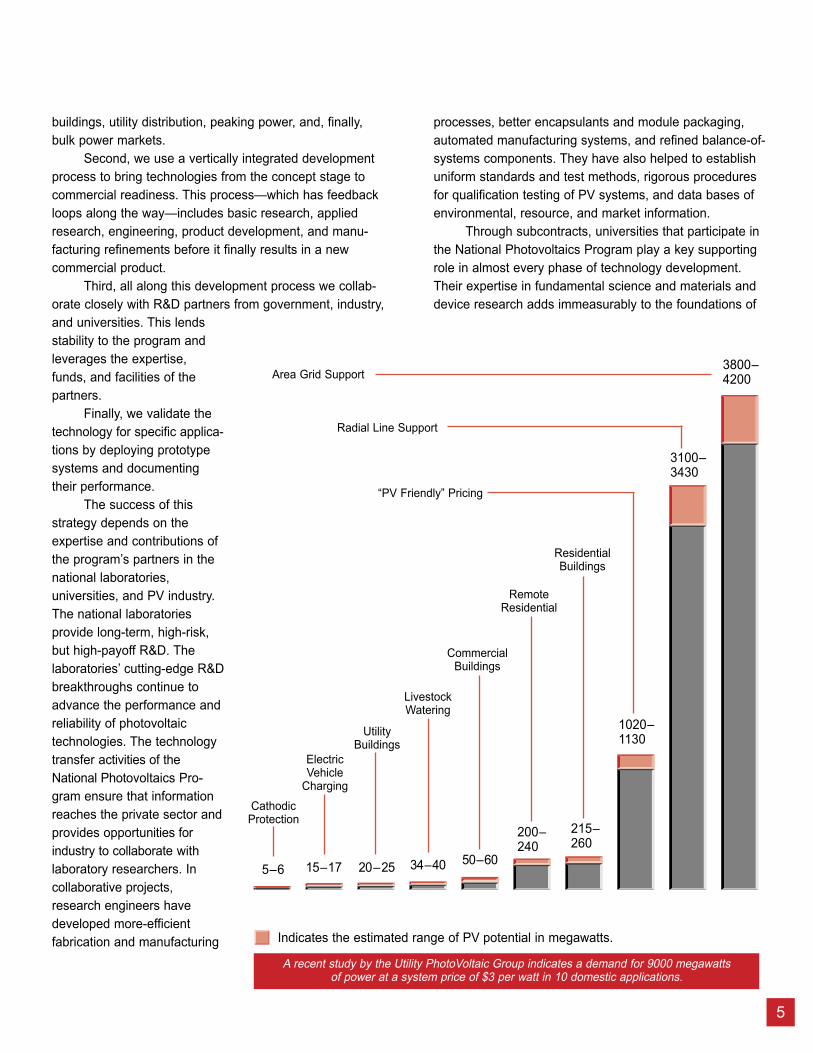
buildings, utility distribution, peaking power, and, finally,bulk power markets.
Second, we use a vertically integrated developmentprocess to bring technologies from the concept stage tocommercial readiness. This process—which has feedbackloops along the way—includes basic research, appliedresearch, engineering, product development, and manu-facturing refinements before it finally results in a newcommercial product.
Third, all along this development process we collab-orate closely with R&D partners from government, industry,and universities. This lendsstability to the program andleverages the expertise,funds, and facilities of thepartners.
Finally, we validate thetechnology for specific applica-tions by deploying prototypesystems and documentingtheir performance.
The success of thisstrategy depends on theexpertise and contributions ofthe program’s partners in thenational laboratories,universities, and PV industry.The national laboratoriesprovide long-term, high-risk,but high-payoff R&D. Thelaboratories’ cutting-edge R&Dbreakthroughs continue toadvance the performance andreliability of photovoltaictechnologies. The technologytransfer activities of theNational Photovoltaics Pro-gram ensure that informationreaches the private sector andprovides opportunities forindustry to collaborate withlaboratory researchers. Incollaborative projects,research engineers havedeveloped more-efficientfabrication and manufacturing
processes, better encapsulants and module packaging,automated manufacturing systems, and refined balance-of-systems components. They have also helped to establishuniform standards and test methods, rigorous proceduresfor qualification testing of PV systems, and data bases ofenvironmental, resource, and market information.
Through subcontracts, universities that participate inthe National Photovoltaics Program play a key supportingrole in almost every phase of technology development.Their expertise in fundamental science and materials anddevice research adds immeasurably to the foundations of
A recent study by the Utility PhotoVoltaic Group indicates a demand for 9000 megawattsof power at a system price of $3 per watt in 10 domestic applications.
3800–4200
3100–3430
1020– 1130
215– 260
200–240
50–6034–4020–2515–175–6
Indicates the estimated range of PV potential in megawatts.
5
Area Grid Support
Radial Line Support
“PV Friendly” Pricing
ResidentialBuildings
RemoteResidential
CommercialBuildings
LivestockWatering
UtilityBuildings
ElectricVehicle
Charging
CathodicProtection

science, the advancement of thetechnology, and the effectivenessof the program.
And through collaborativeinteractions, industry providesfeedback to researchers andengineers on products andprocesses. Industry gives theprogram guidance at all pointsalong the development path. Asan integral member of R&Defforts, industry often assumesthe lead role in the engineeringand product development phasesof a technology’s development.Therefore, in 1995, industryreceived more than 90% ofprogram funding in technologydevelopment and more than 60%of the funding in systems engineering and applications.In the end, it is industry that brings all the efforts of the
National Photovoltaics Programto fruition in the form of lower-cost PV products.
mplementing the Program.Critical to the success of thisstrategy is the NationalPhotovoltaics Program’s effort toreduce the cost of electricitygenerated by photovoltaics. Theprogram is doing this in threeprimary ways: by making devicesmore efficient, by making PVsystems less expensive, and byvalidating the technology throughmeasurements, tests, andprototypes. We accomplish thesetasks under the program’s threemain elements: research and
development, technology development, and systemsengineering and applications.
I
6
PV ApplicationsThe list of actual and potential PV applications
could include nearly anything that requires electricpower.
tand Alone. Photovoltaic systems can supply elec-tricity in areas where there is no electric grid, or whereconnecting to that grid would be too expensive.
Water pumping—Thousands of PV-poweredwater pumps are installed worldwide each year, sup-plying water for households, light industry, agriculture,villages, and livestock. Photovoltaic systems canreplace hand pumps or large engine-powered water-pumping systems, and PV is bringing fresh water toareas that never had wells before.
Cathodic protection—Each year, metal corrosioncauses billions of dollars of damage to pipes, tanks,well heads, wharves, bridges, and buildings buried inearth or installed under water. Photovoltaic-generatedelectricity prevents electrolytic corrosion of suchstructures.
Communications—Today, PV systems arepowering communication systems such as microwaverepeaters, television and radio transmitters andreceivers, telephone systems, and small radios inremote areas.
Lighting and small appliances—In some areas,where there is no electric power available, PV can beused to light single homes, operate a television, orpower a street light. In the developing world, improvingindoor lighting allows small industry to expand, whilereplacing kerosene lanterns improves indoor air quality.In the United States, PV panels and a battery powermany small electrical devices from security lights toswitches.
Village power—In the developing world there arehundreds of thousands of villages without electricpower or that use diesel generators, which are expen-sive to fuel, difficult to maintain, and environmentallyharmful. In the United States there are also communi-ties or enterprises that operate on diesel-powered gen-erators when PV could reduce operating costs andreduce environmental concerns. Photovoltaic villagepower systems provide electricity for any domestic,
S
R&D: using a femtosecond laser to explore fundamentalcharacteristics of PV materials.
Jim
Yos
t Pho
togr
aphy
/PIX
0162
3

Research and development. For photovoltaics tomake a significant contribution to the nation’s energyresource mix, the technology must be improved andelectricity from photovoltaics must become more cost-competitive. Therefore, we continue to conduct basicand applied research on promising new materials,processes, devices, and production techniques. We alsocarefully measure, model, and evaluate new concepts.We perform these R&D activities in three primary areas:thin films, crystalline silicon, and advanced, high-efficiencyconcepts.
Thin films. The program investigates four thin-filmmaterials—amorphous silicon, cadmium telluride, copperindium diselenide, and thin-layer crystalline silicon—because of their potential for low cost and high perfor-mance. As part of its investigations, the program has amajor new initiative—the Thin-Film PV Partnership—underwhich it has awarded cost-shared contracts to nineindustry technology partners and to about 20 universityR&D partners to develop prototype products based on thefour thin-film materials.
For amorphous silicon, the program explores ways inwhich to reach higher conversion efficiencies; to improvethe design and fabrication of multijunction amorphoussilicon alloy cells and modules; and to develop processingtechniques, such as hot-wire deposition, to enhance bothstability and efficiency.
Cadmium telluride devices can be manufactured withmethods that potentially cost very little. But we still need tounderstand this material better, improve the efficiencies ofdevices made from it, achieve uniform stabilities, andtransfer the results to pilot-scale manufacturing.
In 1995, copper indium diselenide achieved a thin-film record efficiency of 17.1% in the laboratory, but prod-ucts using this material are not yet commercially available.Before we can successfully manufacture commercialdevices made with copper indium diselenide we must under-stand phase-change reactions and the effects of temper-ature during fabrication. We must also simplify theproduction process and transfer new techniques to industry.
If constructed to trap light properly, devices madefrom thin-layer crystalline silicon can be more efficient than
7
community, or industrial activity, including operatingcomputers. Photovoltaics can also be used with dieselgenerators, allowing them to run less often.
rid-connected. Innovative uses of PV systemsconnected to the utility grid are being assessed tosupply electricity when and where it will have thehighest value.
Demand-side management—Because powerplants brought on line to serve peak demand periodsare usually the most expensive to operate, electricitygenerated by grid-connected PV systems at peakperiods has the highest value. Utilities strive to smoothout electrical demand with a combination of incentivesto customers called demand-side management.Photovoltaic systems on buildings would operate toreduce peak demand of the buildings. In combinationwith batteries, such systems could also reduce peakloads that occur after sunset. If such systems could becalled upon or “dispatched” by the utility like otherforms of generation they would have even greatervalue.
Transmission and distribution support—Aselectrical demand increases in portions of a utility
company’s service territory, the transmission anddistribution system may need to be expanded. Thiscan be quite expensive, requiring new largertransformers and possibly larger distribution lines.Installing PV generation near substations or at the endof overloaded lines can eliminate or delay the need forcostly upgrades. By helping the utility avoid expensiveupgrading, the electricity generated by the PV systemhas greater value.
Bulk power generation—Large-scale generationof electric power is an important long-term applicationfor photovoltaics. Although not cost-effective at today’sPV system prices, the cooperative research of theNational Photovoltaics Program aims to push downthe cost of electricity generated by PV systems to thepoint of being competitive with other widely used formsof generation.
ther. The list of actual and potential PV applica-tions is large and growing larger. It includes vaccinerefrigeration, consumer products, space power appli-cations, pond aeration, electric-vehicle charging, andothers too numerous to mention.
O
G

8
other thin-film devices. To achieve this aim, the program isexploring ways in which to make the material less than 50micrometers thick, is researching a low-cost substrate andbuffer layer, and is developing better light-trapping andinterconnection schemes.
Crystalline silicon. Under theCrystalline Silicon ResearchCooperative, the program exploresmethods with which to achievehigher efficiency devices made withless expensive, industrial-gradesilicon. The program alsoinvestigates how material impuritiesreduce the efficiency of devices;this understanding will enablemanufacturers to compensate for oravoid these defects.
Advanced, high-efficiencyconcepts. We develop advancedtechnologies for specializedmarkets, such as PV concentratorsystems. These include highlyefficient (32% goal in the nearterm), single- and multijunctiondevices based on gallium arsenide and related III-V alloymaterials. Industry efforts in this area are driven by spacemarkets today. The program also investigatesthermophotovoltaic devices, which convert thermal radiationto electrical energy.
Technology development. To translate laboratoryinnovations into technical improvements for commercialproducts, the National Photovoltaics Program investigatesthree areas: manufacturing technology, module develop-ment, and balance-of-system (BOS) components.
Manufacturing technology. Through collaborations,industry and the National Photovoltaics Program havereduced module production costs by as much as 50%during the last 5 years, and hope to decrease them byanother factor of 2 during the next 5 years. This theyintend to do by increasing throughput; by modifyinglaboratory techniques for production; by assessing newmanufacturing processes and finding better ways to scaleup manufacturing processes; by measuring, analyzing, andcharacterizing PV materials and devices; and bysimplifying PV systems and incorporating the most durable,cost-effective components possible.
Most of this work is performed under the auspicesof the PVMaT (PV Manufacturing Technology) initiative.
It addresses manufacturing R&D for crystalline silicon,concentrators, and various thin-film technology options.
Module development. Through measurements, analy-sis, accelerated testing, and collaborative R&D, the
National Photovoltaics Programintends to produce better,stronger encapsulants and toimprove the performance, dura-bility, and lifetime of photovoltaicmodules.
Balance-of-system compo-nents. Although balance-of-system components, such asinverters, batteries, supportstructures, junction boxes, andcontrol systems represent just halfthe cost of PV systems, they areresponsible for as much as 99%of system failure and repairproblems. The goal here is toincrease the efficiency of thesecomponents, increase theirreliability through optimizeddesigns, and reduce their costs
through mass production. Systems engineering and applications. To help
industry improve the performance, reliability, and opera-tional characteristics of its products, the National Photo-voltaics Program tests and evaluates the material,mechanical, electrical, and safety characteristics of cells,modules, BOS components, and complete systems. Underthis program element, the new outdoor test facility at theNational Renewable Energy Laboratory (NREL) will sup-port program activities with numerous test results of proto-type and precommercial modules.
To help products become accepted in potentialmarkets, the PV Program helps industry and standardsgroups develop national and international safety andreliability standards appropriate for PV products.
To validate prototype PV technologies, the programdeploys systems in stand-alone and utility-tied domesticand international applications and measures and analyzestheir performance. These projects help demonstrate themost cost-effective PV applications for key markets.
For domestic applications, the program works closelywith groups of users—such as the National Parks Service,Forest Service, military agencies, and utilities—who repre-sent large markets for PV systems.
Technology development: addressing manufacturingR&D through the PVMaT initiative.
AS
EA
mer
icas
/PIX
0156
1

For international applications, the program has pilotprojects in several nations and works with agencies fromthese nations, international lending agencies, specificsystem users, and nongovernment organizations.
The majority of the workunder this program elementinvolves crystalline silicon photo-voltaics, although the activitieswill benefit future thin-filmPV technologies.
uiding the Effort. In one sense,this collaborative program is guidedby representatives of all its partici-pants in national laboratories,industry, and universities. Morespecifically, PV Programmanagers in DOE’s Office ofEnergy Efficiency and RenewableEnergy, and in the nationallaboratories, developcomprehensive operating plansbased on strategic, multiyearplans such as this one, whichrespond to the broad policies for energy R&D determinedby the Executive and legislative branches of the federalgovernment.
Through sound management practices and continualfine-tuning, program managers ensure that the budgetallocations, direction, and individual elements of the
National Photovoltaics Program meet the objectives of thenation and stay on target. Individual project and researchmanagers at the national laboratories and DOE’s field officesadminister both in-house research and cost-shared R&D
contracts with the private sector.Federal funding for the PV Pro-gram was nearly $75 million inFY 1994 and $84 million in FY1995. Industrial partners typicallycost-share the contract researchefforts, 50-50, in the program.In addition, private-sector invest-ments in developing manufac-turing facilities exceed thegovernment investment in R&Dby a factor of 2 or more. Otherinvestments and new financingare also crucial to our success.Large national and multinationalprojects require the participationof international development andfinancing organizations.
Future program-sponsoredR&D activities will continue to
explore new and better ways to convert sunlight to electricityand to assist promising young industries in becoming self-sustaining. The promise of photovoltaics will be fulfilledwhen this versatile, operationally simple technology is fullyable to meet a significant share of the needs of our nation—and the entire world—for clean, affordable electricity.
G
9
Systems engineering and applications: deploying andevaluating systems in a variety of applications.
1991 1995 2000 2010–2030
40–75Electricity price(¢/kWh)
25–50 12–20 <6
5–14Moduleefficiency* (%)
7–17 10–20 15–25
10–20System cost($/W)
7–15 3–7 1–1.50
5–10System lifetime(years)
10–20 >20 >30
75U.S. cumulativesales (MW)
175 400–600 >10,000
Photovoltaic progress and program goals (costs and prices in 1995 dollars)
*Range of efficiencies for commercial flat-plate and concentrator technologies.
Sol
ar E
lect
ric L
ight
Fun
d/P
IX01
543

10
In Austin, Texas, a 300-kilo-watt concentrator systemsupplies part of the powerfor the 3M Company’sresearch center.
3MC
ompa
ny/P
IX00
014
The potential of PV goes wellbeyond its versatility as an energytechnology. Photovoltaics also holdsgreat economic and environmentalpromise.
As an energy technology,photovoltaics can be used for almostanything that requires electricity—fromsmall, remote applications to largecentral power stations. This is not only aversatile technology that gives ournation a wide range of choices forgenerating electricity, it is also a home-growntechnology that depends only onsunlight for fuel and domestic materialsfor construction.
Photovoltaics is also an emergingtechnology that will help our nation’seconomy grow. There are alreadythousands of PV systems in use acrossthe nation. And the Utility PhotoVoltaicGroup estimates that, as system costsdrop below $3 per watt, we may see thedomestic demand rise to greater than9000 megawatts. This would make PV amultibillion dollar industry generatingthousands of well-paying jobs.
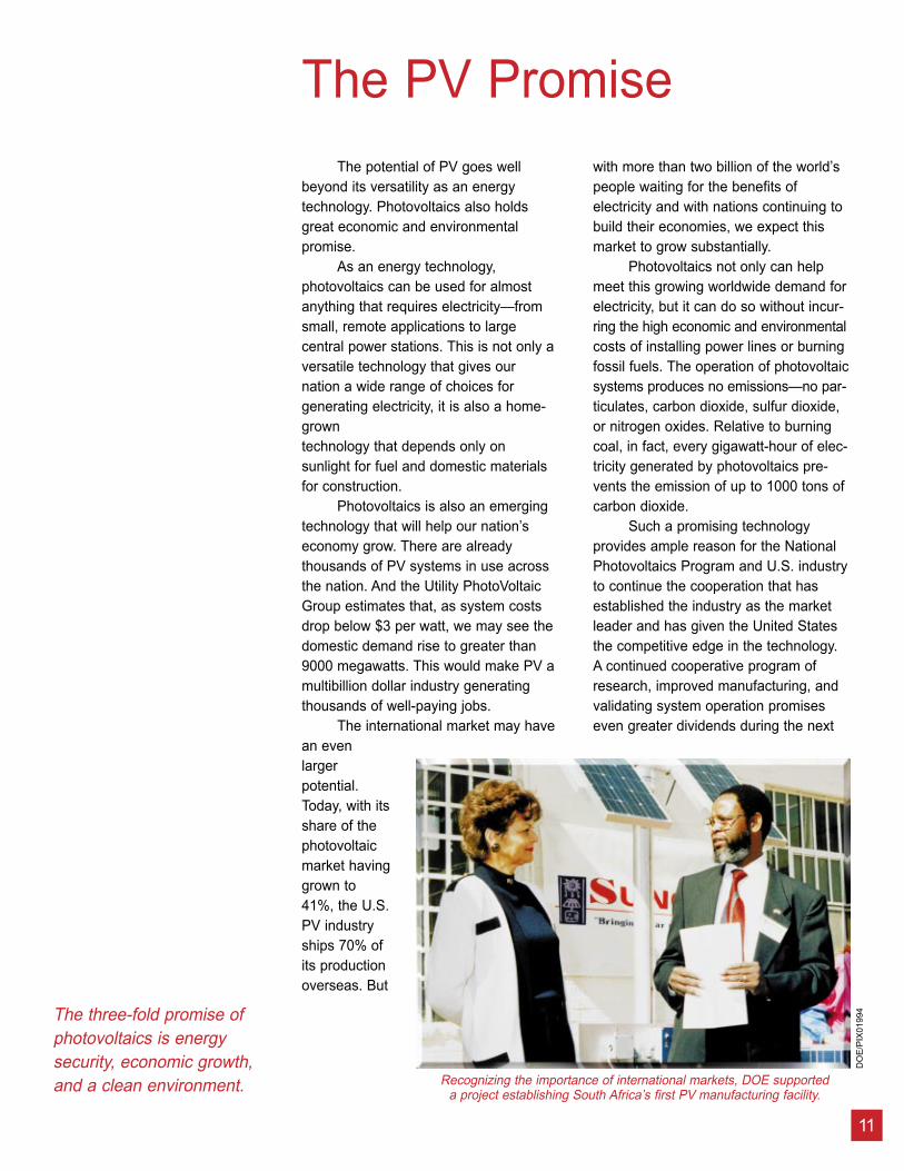
The international market may havean evenlargerpotential.Today, with itsshare of thephotovoltaicmarket havinggrown to41%, the U.S.PV industryships 70% ofits productionoverseas. But
with more than two billion of the world’speople waiting for the benefits ofelectricity and with nations continuing tobuild their economies, we expect thismarket to grow substantially.
Photovoltaics not only can helpmeet this growing worldwide demand forelectricity, but it can do so without incur-ring the high economic and environmentalcosts of installing power lines or burningfossil fuels. The operation of photovoltaicsystems produces no emissions—no par-ticulates, carbon dioxide, sulfur dioxide,or nitrogen oxides. Relative to burningcoal, in fact, every gigawatt-hour of elec-tricity generated by photovoltaics pre-vents the emission of up to 1000 tons ofcarbon dioxide.
Such a promising technologyprovides ample reason for the NationalPhotovoltaics Program and U.S. industryto continue the cooperation that hasestablished the industry as the marketleader and has given the United Statesthe competitive edge in the technology.A continued cooperative program ofresearch, improved manufacturing, andvalidating system operation promiseseven greater dividends during the next
The PV Promise
The three-fold promise ofphotovoltaics is energysecurity, economic growth,and a clean environment.
11
Recognizing the importance of international markets, DOE supporteda project establishing South Africa’s first PV manufacturing facility.
DO
E/P
IX01
994

12
A researcher uses a hailtester to determine theability of a PV module towithstand the impact ofhail stones.
Jim
Yos
t Pho
togr
aphy
/PIX
0182
0

The challenge before us is toenable photovoltaic technology to fulfillits energy, economic, and environmentalpromise. By doing so, we will also fulfillour mission of helping PV become asignificant part of the U.S. economy.
To meet this challenge, we mustadvance the status of photovoltaictechnology and strengthen the industry.Toward this end, we have establishedimportant goals for the next 5 years.
First, we must make photovoltaicsmore cost-competitive with other formsof electrical generation. Today’s PV sys-tems are in fact cost-competitive inmany applications, particularly in ruralareas. By 1996, the U.S. PV industryhad installed a total of 210 megawatts ofPV generating capacity worldwide. Butwe need to reduce the cost of photo-voltaics even further to be competitive ina wider range of applications, includingsome grid-connected uses. Our goal inthis regard is for PV to produce elec-tricity at 12 to 20 cents per kilowatt-hourby the year 2000.
Second, we must make photo-voltaics as reliable and convenient to
use as the next best alternative for eachapplication. The attractiveness of photo-voltaics to consumers includes all aspectsof reliability, convenience, and appro-priateness for its applications.
The National Photovoltaics Pro-gram plan addresses these issues. Thecooperative R&D projects described inthis plan will increase the reliability ofPV components, reduce system costs,and increase system efficiencies. Andthe systems engineering and applica-tions elements of the program will vali-date prototype system performance inkey applications.
As we meet these goals we willsee new markets open up and old onesflourish. In fact, by the year 2000, weexpect the U.S. PV industry to haveinstalled between 400 and 600 mega-watts cumulative. Such a market willhave enabled the U.S. PV industry tomore than treble its industrial base—along stride toward having fulfilled thechallenge and the promise of photo-voltaic technology and toward havingmet the mission of the National Photo-voltaics Program.
The PV Challenge
A modular PV system is installed at a remote Navajo home to provide cost-effective electricity.
To help PV meet itspromise, we must makethe technology morecompetitive and makePV systems more reliableand efficient.
13
San
dia/
PIX
0155
9
14
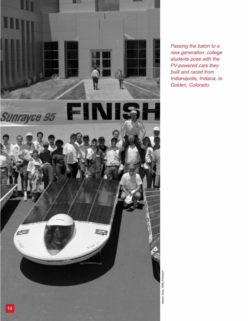
Passing the baton to anew generation: collegestudents pose with thePV-powered cars theybuilt and raced fromIndianapolis, Indiana, toGolden, Colorado.
War
ren
Gre
tz, N
RE
L/P
IX00
237

To meet the challenge we face inmaking PV an important part of our ener-gy mix and our economy, the NationalPhotovoltaics Program uses a four-pronged strategy: First, we work in closeconcert with industry and other stake-holders to develop specific goals thatserve as significant milestones on thepath to achieving a PV technology com-petitive with other sources for generatingelectricity.
Second, we use an approachknown as vertical integration to bringtechnologies from the concept stage tocommercial readiness. Here, the govern-ment’s role spans most of a long pro-cess that includes basic research,applied research, engineering, productdevelopment, and manufacturing beforeit finally results in a new commercialproduct. The privatesector has anincreasing role, andthe government adecreasing role, astechnologies pro-gress through tocommercialization,which is entirely aprivate-sectorresponsibility.
Third, we aug-ment vertical integra-tion with collaborativeprojects in which theR&D partners—government, indus-try, and universities—play important roles.This process pro-motes “buy-in” fromthe partners andlends stability and
direction to the program. It allows “mid-course corrections” in the developmentof a technology. It leverages the exper-tise, the facilities, and funds of the part-ners. And it guides concepts accordingto their final usefulness, which makesthe successful development of a tech-nology more likely.
Finally, we deploy and documentthe performance of prototype systems tovalidate the technology for specific appli-cations. Key to validating a technology isdrawing stakeholders into the process,to inform them of PV’s benefits and togain information about barriers to appli-cations that the program could addressand overcome.
The success of this strategydepends on the expertise and contribu-tions of the major partners in the PV
15
Meeting the Challenge
Marketing
Manufacturing
Product Development
Engineering
Applied Research
Basic Research
The PV Program uses a vertically integrated process, withfeedback loops all along the development path.
The PV Program uses a four-pronged strategy to helpmake PV an important part ofthe nation’s energy mix andeconomy: goal development,vertical integration,collaboration with industryand academia, andtechnology validation.

Program in the national laboratories, university researchgroups, and the PV industry.
he Laboratories. Through insights in physics,chemistry, electronics, optics, materials science, andsurface science, national laboratory scientists have helpedPV become a sophisticated technology.
Engineers and researchers help develop advanceddevices and modules, new PV materials and material com-binations, more-efficient fabrication and manufacturing pro-cesses, better module encapsulants, more sophisticatedconcentrators and sun-tracking equipment, and automatedmanufacturing systems. They also help improve PV systemdesigns and refine balance-of-system components, includ-ing support structures, power-processing and controlsequipment, electronics, monitoring equipment, and storagetechnologies.
Specialists work with national and internationalorganizations to establish uniform standards and testmethods. Rigorous testing ensures that the electrical,mechanical, and safety aspects of PV systems are sound.Analytic studies—including the results of environmental,resource, and market assessments—have an importantimpact on current and future R&D activities.
The laboratories also serveas incubators for new ideas.Because most companies cannotafford large R&D laboratories, thenational laboratories provide long-term, high-risk, high-payoff R&D,which is tantamount to investing inthe nation’s future—toward clean,sustainable, affordable electricity.
niversities. Universities play akey supporting role in almost everyphase of technology development,from basic research to developingnew manufacturing processes todeploying and testing prototypesystems. The DOE has designatedtwo Centers of Excellence in PV atGeorgia Institute of Technology andthe Institute of Energy Conversionat the University of Delaware. These and other universitiesparticipate in the Thin-Film PV Partnership teams and theCrystalline Silicon Research Cooperative. By tapping intothese skills, the PV Program not only leverages the talentand facilities available in the universities, it also helps to
prepare the nation’s nextgeneration of scientists andengineers.
The PV Program alsoconducts programs to attractthe interest and talents of theacademic community. TheUniversity ParticipationProgram for PV Researchattracts university researchteams to promote basic andapplied research ideas in anenvironment of free-spiritedstudy. The biennial Sunraycechallenges students to design,build, and race PV-poweredcars. And an initiative with Historically Black Colleges andUniversities (HBCUs) strengthens the research andeducational capabilities of HBCUs in photovoltaics.
ndustry. To be relevant and cost-effective, R&D musthave the feedback only industry can provide. Throughcollaborations, consultations, and membership on advisoryand planning boards, industry provides the program with
direction at all points along atechnology’s development path.
Plus, as an integral mem-ber of R&D’s efforts, industryoften assumes the lead role inthe engineering and productdevelopment phases of atechnology’s development cycle.Such is the case, for example,with the PVMaT project. Here,more than 20 companies havejoined with DOE in an extremelysuccessful, cost-shared effort toovercome persistent barriers tomore-efficient, more-productivemanufacturing processes.
Other examples ofindustry’s collaboration with thePV Program include the Thin-Film PV Partnership, a cost-
shared project that is accelerating the efforts of manufac-turers to bring thin-film materials to pilot production; theCrystalline Silicon Research Cooperative, which is increas-ing the efficiency of devices made from crystalline silicon,while decreasing costs and increasing reliability; and
I
U
T
A student researcher at Colorado School of Minesuses Raman scattering to analyze PV materials.
Solar Energy Research Facility in GoldeLabortory does world- class
16
Jim
Yos
t Pho
togr
aphy
/PIX
0181
4

17
balance-of-system cost-shared R&D, in which DOE andindustry seek to manufacture high-quality system compo-nents while drastically cutting costs.
These augment and expedite the progress of the PVProgram and assist a young but growing industry in pro-ducing clean, affordable PV systems.
rogram Goals. The PV Program’s cooperativeapproach has achieved some remarkable results and iswell suited to meeting the challenge of the next 5 years.Efficiencies have increased for each technology. Newmanufacturing approaches have been transferred toindustry in record time. We see products entering themarket today, like the cadmium telluride module, that wereonly laboratory curiosities in 1991. And PV systems acrossthe world have proven to bereliable and cost-effective.
One benchmark formeasuring technical progressin photovoltaics is efficiency—the percentage of sunlightfalling on a PV device that isconverted to electricity.Because the resource is freeand renewable, PV systemefficiency is not comparableto that of other energy tech-nologies; but it must beconsidered along with costand ease of manufacture asan indicator of PV’sattractiveness and suitability.
Over the next 5 years,the PV Program will focus on
transferring techniques for achieving high laboratoryefficiencies to industry, where they can be evaluated fortheir potential to yield lower-cost production modules.
To be attractive in more applications, PV systemsmust also last a long time. System lifetimes have doubledsince 1991, and manufacturers are providing warranties ofup to 20 years on modules. Under this 5-year plan, theprogram will conduct field measurements and acceleratedtesting to help extend the useful life of systems to 20 yearsor more—important for reaching our long-term goal ofsystems that last at least 30 years.
The price of PV electricity is also an important indi-cator of the most promising PV applications. We have madesteady progress toward our long-term goal of matching theprice of electricity generated by fossil fuel or nuclear gener-ating plants. Our mid-term goal of 12 to 20 cents per kilo-watt-hour is achievable, but depends on several factorsincluding installed production capacity.
Module manufacturing costs have dropped signifi-cantly, especially with the help of the program’s PVMaTproject. But manufacturing costs must decline even moreto help PV compete in wider applications.
Over the next 5 years, PV system costs shoulddecline an additional factor of 2, reflecting continued workon improved PV technologies, module manufacturing,balance-of-system components, and integration of systemcomponents into PV products ready for markets.
For PV to become a more important part of oureconomy, the market must grow and the industry mustexpand. One measure of the size of the PV industry is
cumulative sales of U.S.-made PVsystems. We expect cumulative salesto be between 400 and 600megawatts by the year 2000 as acondition for continued industrialexpansion.
To reach our goals, we mustimprove our fundamental understand-ing of materials, processes, anddevices; develop new and better low-cost processes and technologies;continue to transfer and scale uplaboratory results; reduce module andbalance-of-system costs; improve thereliability and durability ofcomponents and systems; validatenew systems, applications, andtechnologies; and help overcomemarket and institutional barriers.
P
ility in Golden, Colorado. This DOEfacility at the National Renewable Energyworld- class research for in-house, industry, and university projects.
War
ren
Gre
tz, N
RE
L/P
IX01
347
Golden Photon, Inc., is one of two companies makingmodules of the new material, cadmium telluride.
Dav
id P
atry
as P
hoto
grap
hy/P
IX01
545

18
X-ray photoelectronspectroscopy is used toobtain critical information onchemical bonding andmolecular structure of PVmaterials.
Jim
Yos
t Pho
togr
aphy
/PIX
0143
7

For photovoltaics to meet itspromise as an energy technology,expand its markets worldwide, and makea significant contribution to our nation’senergy mix, we must improve the tech-nology so that PV systems will be reli-able and durable and will deliverelectricity at competitive prices.
Reducing the cost of electricityfrom PV systems is the chief goal drivingour technology R&D program. Theprogram works in three ways to makePV cost-competitive: by making devicesmore efficient and reliable, by makingsystems less expensive, and by validat-ing the technology.
To accomplish our aim we havecarefully crafted a program that main-tains a balance between basic researchand technology applications. Each of thethree major elements of this program—research and development, technologydevelopment, and systems engineeringand applications—is guided by technicalgoals.
Research and development. In thisarea, scientists conduct basic andapplied research on promising newmaterials, processes, devices, and
production techniques. In concert withindustry, DOE researchers move ideasfrom the drawing board to the laboratorybench-scale and prototype development.Key to the success of this program ele-ment is the evaluation of new conceptsand materials through careful measure-ments and modeling.
Technology development. Translat-ing laboratory innovations in materials,processing, and system operation is thechallenge of the technology develop-ment portion of the program. Throughindustry-directed research partnerships,the program advances PV manufactur-ing technologies, reduces moduleproduction costs, increases module per-formance, improves balance-of-systemcomponents, and expands U.S. pro-duction capacities.
Systems engineering and applica-tions. Under this element, the programmeasures and documents the perfor-mance of photovoltaic systems anddisseminates information on PV charac-teristics. The program also conductsprojects that demonstrate the per-formance and value of PV systems inapplications for key markets.
Implementing the Program
To advance the technology,the PV Program uses acarefully crafted approachwith three balanced andintegrated elements—research and development,technology development, andsystems engineering andapplications. Each element isguided by technical goals. Researchers use Sandia’s PV Device Fabrication Laboratory to
design, make, and test crystalline silicon solar cells.
19
Jim
Yos
t Pho
togr
aphy
/PIX
0352
5

Research and developmentgenerates new approaches byturning researchers’ ideas intolaboratory experiments and proto-type devices. In this area, theNational Photovoltaics Programconducts R&D in thin films, crys-talline silicon, and advanced,high-efficiency concepts.
hin Films. Thin films are apromising path to low-costphotovoltaics, and at least eightU.S. companies are planning orbuilding thin-film photovoltaicmanufacturing plants in 1995. Thistransition to first-time manu-facturing is a period of extremetechnical and financial risk.Moreover, for thin-film products toreach their low-cost potential,additional research is needed todevelop materials and processesyielding devices with higherefficiencies, more uniform performance over the entiresurface area of modules, and lower production costs.
But high-technology research is expensive, and theshort-term payoff is uncertain for today’s PV companies.Therefore, DOE support remains crucial. By combining thetalents of scientists performing fundamental research withengineers developing prototype modules, the PV Programcan help ensure that a continuous stream of advanced thin-film technology is incorporated into future manufacturingfacilities.
In 1995, under the Thin-Film PV Partnership program,DOE awarded major contracts to 9 industrial partners andto about 20 research partners in universities. Through theyear 2000, each of the partners will contribute 10% to 50%of the value of these contracts. University researchers,including those at the DOE PV Center of Excellence at theInstitute of Energy Conversion at the University ofDelaware, play key roles in these efforts. These collabora-tions will develop prototype products largely based onamorphous silicon, cadmium telluride, copper indiumdiselenide, and thin-film crystalline silicon technologies.
Amorphous silicon. The first thin-film amorphoussilicon devices made in 1974 had efficiencies of less than1%. By 1994 a small, experimental module recorded astabilized efficiency of 10.2%. Although amorphous siliconmaterials have lower efficiencies than crystalline silicon,
they have the potential to be lessexpensive to manufacture. Todaymore than 15% of worldwide PVproduction uses amorphoussilicon technology.
Most products using amor-phous silicon are low-powerconsumer items like solarwatches and calculators. Higher-power applications will demandamorphous silicon products withhigher stabilized efficiencies sothat more energy can be extract-ed from a given module area.Our research goal during thenext 5 years is to raise efficien-cies for our best laboratory cellsfrom today’s 10% to 13%.
Key to the process istransferring to industry anytechniques we perfect in thelaboratory. To increase theefficiency of amorphous siliconPV, more than 40 researchers
nationwide are working under the Thin-Film PV Partnershipprogram. These research teams are addressing a dozenissues surrounding the design and fabrication of multi-junction amorphous silicon alloy cells. For example, oneteam is optimizing back reflectors that direct unused sun-light back up through the thin layers of a multijunction cell.Another team is modeling the effects of using various
T
20
Research and Development
Hot-wire deposition promises to improve the efficiency andstability of amorphous silicon devices.
Progress and goals for efficiencies of the beststable amorphous silicon cells and modules.
2000*19951991
9%
10%
13%
6%
8%
10%
4%
6%
9%
Laboratorycell
Prototypemodule
Commercialmodule
*Module goals are for those larger than 4000 cm2.
Jim
Yos
t Pho
togr
aphy
/PIX
0181
3

combinations of alloys and thicknesses in the multijunctionlayers and is investigating new structures. Other teams areimproving the output from the individual component cells inthe multijunction device.
In addition, researchers are developing ways toprocess amorphous silicon material that improve itsstabilized efficiency. The most-promising approach to dateis hot-wire deposition. The extremely hot (2000°C)temperatures of the wire cause dissociation of the feedgases and deposition of the active radicals at rates up to 10times higher than the glow-discharge method used inindustry today. The resulting material contains less hydro-gen, the agent suspected as the cause of amorphoussilicon’s instability. Tests in early 1995 indicated that materialcreated with the hot-wire method is much more stable thanconventional amorphous silicon; later tests showed thatefficiency can approach the state of the art. Future work willinvestigate the viability of this alternative approach toreplace existing processes.
By 2000, working with industry on device design andmaterial deposition techniques, our goal is to improve thestabilized efficiency of laboratory amorphous silicondevices. Moreover, our research results can be transferredto the production line because there is a mature manu-facturing base for amorphous silicon. The progress ofamorphous silicon, from technical conception throughmanufacturing maturity and ongoingtechnical progress, has been atriumph of past DOE partnershipswith industry. We expect the futureto yield the fruits of such acombined approach.
Cadmium telluride. TheNational Photovoltaics Program isexploring cadmium telluridebecause the techniques used tomanufacture devices from thismaterial—including elec-trodeposition, spraying, and high-rate evaporation—are potentiallyvery low-cost. It also promises highefficiencies—small laboratorydevices have reached nearly 16%,although commercial moduleefficiencies hover around 6%. TwoU.S. companies are preparing tobring prototype products to marketthat should compete withestablished products made fromcrystalline silicon.
Our goal is to convert the high cell efficiencies wehave achieved in the laboratory into more-efficient produc-tion modules.
Increasing module efficiencies is challenging because,despite our progress, our fundamental understanding of
the properties of cadmium tellurideis limited. For example, somemodules have exhibited stableperformance for 6 years outdoors,while others have shown significantdeclines in efficiency in a matter ofdays. The mechanisms of thisuncertain stability have yet to befully characterized.
In addition, researchers oftenachieve high cell efficiencies usingapproaches that are far from beingavailable to manufacturers. Forexample, high-quality 7059 glass isused for the best cells, but it is tooexpensive to be used in production(where soda lime glass is used).The high efficiencies of small-areacells are due in part to the deposi-tion of very thin layers of cadmiumsulfide. No one has learned how toachieve such a thin layer in amodule-scale device; a thicker layerreduces efficiency by about 25%.
21
Scientists use close-spaced sublimation as one way to makeand study high-efficiency cadmium telluride devices.
Progress and goals for efficiencies of the bestcadmium telluride cells and modules.
2000*19951991
12.5%
15.8%
18%
6%
8.4%
10%
6%
9%
Laboratorycell
Prototypemodule
Commercialmodule
*Module goals are for those larger than 4000 cm2.
Jim
Yos
t Pho
togr
aphy
/PIX
0150
4

22
To meet challenges likethese, 25 researchers nationwideare working in teams under theThin-Film PV Partnership program.One team is studying instability incadmium telluride materials anddevices to learn how to design andbuild stable modules. Another teamis working to adapt laboratory cell-fabrication techniques for large-scale production. These effortsshould help the photovoltaic R&Dcommunity realize the potential ofhigh-efficiency cadmium telluridecells for high-efficiency powermodules.
Copper indium diselenide.In 1995, researchers pushed theefficiency for devices based oncopper indium diselenide to17.1%, the highest efficiencyrecorded for any thin-film cell. A prototype power modulehas been measured at 10.2%. And copper indiumdiselenide is the only thin-film material with many years ofoutdoor exposure that shows no deterioration inperformance. Yet, in 1995 there were no commercialproducts based on this material and its alloys.
Copper indium diselenide is not yet commercialbecause significant further research is needed to under-stand the manufacturing processes. Fabricating high-quality films requires making a copper-rich layer and acopper-poor surface layer to form a junction with otheralloys. Researchers in this technology have difficultyavoiding defects that prevent the formation of uniformlayers. Using proper temperatures and correctly timingthe process steps are critical to achieving quality results.
To reach the goal of manufacturing commercial cop-per indium diselenide products, 40 researchers nationwideare working to devise simpler, more-effective fabricationmethods as part of the Thin-Film PV Partnership program.Basic to this activity is a better understanding of the chemi-cal and physical properties of this material. Researchers inthe program have learned much about how the variouselements and compounds combine to form quality copperindium diselenide. And the more we understand about tem-perature, phase-change reactions, and which steps canprecede others, the better we can simplify the process foradaptation to industry.
Thin-layer crystalline silicon.Although crystalline silicon absorbssunlight about 10 to 100 times lesseffectively than other thin films,thin-layer crystalline silicon cellscan be more efficient than thosemade of other thin-film materials ifproperly constructed to trap light.The advantage to using silicon isthat it is familiar and well-studied.
So far, researchers havedeposited relatively thick layers ofcrystalline silicon on low-costsubstrates. Future work will focuson thinning the material to lessthan 50 micrometers, while devel-oping optimal substrate, light-trap-ping, and interconnection schemes.
rystalline Silicon. Crystallinesilicon is likely to continue to
dominate PV markets at least through the year 2000. Withits relatively high efficiency, stability, competitive cost, andproven track record, it plays a dominant role in bothdomestic and international markets. In 1994, modulesmade of crystalline and multicrystalline silicon accountedfor about 95% of all the modules sold by U.S. PVmanufacturers.
Today’s crystalline silicon devices are more efficientthan ever before. Laboratory cells made from single-crystalsilicon have measured efficiencies as high as 24%.
C
The program has developed a new approach for mak-ing high-efficiency copper indium diselenide devices.
Progress and goals for efficiencies of the bestcopper indium diselenide cells and modules.
2000*19951991
13%
17.1%
20%
9%
10.2%
13%
10%
Laboratorycell
Prototypemodule
Commercialmodule
*Module goals are for those larger than 4000 cm2.
Jim
Yos
t Pho
togr
aphy
/PIX
0352
4

Research on manufacturingimprovements has pushed theefficiencies of multicrystallinedevices to nearly 18% for labora-tory cells and over 15% for proto-type modules. Commercialmodules of 14% efficiency aremade in production.
Over the next 5 years, ourresearch will focus on reducing thecost of electricity from commercialflat-plate modules by increasingthe efficiency of low-cost materi-als. The low-cost silicon used byindustry has lower efficienciesthan the pure silicon used in thelaboratory. Defects and impuritiesin the material interfere with photo-electric conversion and the trans-mission of electrons within thecells and modules. Armed with anunderstanding of the microscopicand atomic processes at work, researchers are workingwith industry to devise techniques of material growth anddevice processing that circumvent or compensate for theseimpurities and defects.
We are also working with industry to push the effici-ency limits of pure silicon-based devices. The emitter-wrap-through cell, for example, employs both positive andnegative electrical contacts on the cell’s back surface. Thistechnology could reduce manufacturing costs and preventcurrent losses due to shading by grid lines.
Increasing the efficiency of crystalline materialsthrough improved processing is a major goal of the PV Pro-gram’s Crystalline Silicon Research Cooperative, whosepartners include six U.S. manufacturers and the nationallaboratories. Sandia and NREL researchers characterizematerials prepared by industry to help them assesschanges in manufacturing processes. Universityresearchers, including those at the DOE PV Center ofExcellence at Georgia Institute of Technology, also play akey role in these efforts.
dvanced, High-Efficiency Concepts. The National Photo-voltaics Program also supports emerging advanced, high-efficiency technologies for specialized markets, includingconcentrator systems. These technologies include galliumarsenide, with a measured single-junction efficiency greaterthan 25% at 1-sun and nearly 28% under concentrated
sunlight, and multijunction cellsbased on gallium arsenide andrelated III-V alloys, withconversion efficiencies greaterthan 30%. We expect to exceed32% efficiency using thesedevices in concentrator systems.Industry efforts in this area aredriven by space markets today.
High-efficiency deviceresearch improves our under-standing of the electronicprocesses in PV devices so thatwe can better control the factorsthat cause losses in efficiency.Improvements in basic scienceresulting from this work are oftenapplicable to all other technologyareas in ways that cannot beanticipated. For example, thesematerials may result in very highefficiency thin films (greater than
25%). Continued support for cutting-edge science throughuniversities, research centers, national laboratories, andindustry is an important aspect of the PV Program.
A
Progress and goals for efficiencies of the best single-crystal silicon cells and modules.
200019951991
23.1%
24.0%
25%
17%
21.6%
22%
15%
15.3%
18%
13%
14%
15%
Laboratorycell
Laboratorymodule
Commercialprototype*
Commercialmodule
*Figures are for prototype modules on commercial material.
23
A commercialized NREL invention uses laser beam-induced-current maps to analyze silicon materials.
Bhu
shan
Sop
ori,
NR
EL/
PIX
0352
1
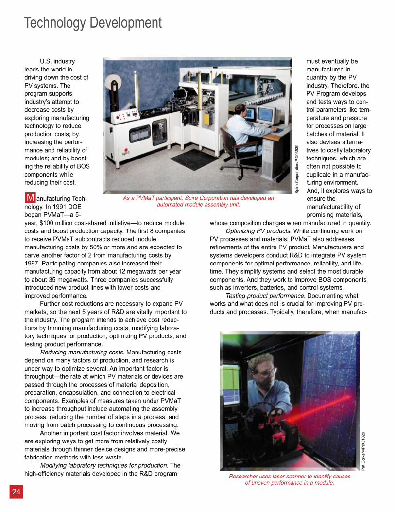
U.S. industryleads the world indriving down the cost ofPV systems. Theprogram supportsindustry’s attempt todecrease costs byexploring manufacturingtechnology to reduceproduction costs; byincreasing the perfor-mance and reliability ofmodules; and by boost-ing the reliability of BOScomponents whilereducing their cost.
anufacturing Tech-nology. In 1991 DOEbegan PVMaT—a 5-year, $100 million cost-shared initiative—to reduce modulecosts and boost production capacity. The first 8 companiesto receive PVMaT subcontracts reduced modulemanufacturing costs by 50% or more and are expected tocarve another factor of 2 from manufacturing costs by1997. Participating companies also increased theirmanufacturing capacity from about 12 megawatts per yearto about 35 megawatts. Three companies successfullyintroduced new product lines with lower costs andimproved performance.
Further cost reductions are necessary to expand PVmarkets, so the next 5 years of R&D are vitally important tothe industry. The program intends to achieve cost reduc-tions by trimming manufacturing costs, modifying labora-tory techniques for production, optimizing PV products, andtesting product performance.
Reducing manufacturing costs. Manufacturing costsdepend on many factors of production, and research isunder way to optimize several. An important factor isthroughput—the rate at which PV materials or devices arepassed through the processes of material deposition,preparation, encapsulation, and connection to electricalcomponents. Examples of measures taken under PVMaTto increase throughput include automating the assemblyprocess, reducing the number of steps in a process, andmoving from batch processing to continuous processing.
Another important cost factor involves material. Weare exploring ways to get more from relatively costlymaterials through thinner device designs and more-precisefabrication methods with less waste.
Modifying laboratory techniques for production. Thehigh-efficiency materials developed in the R&D program
must eventually bemanufactured inquantity by the PVindustry. Therefore, thePV Program developsand tests ways to con-trol parameters like tem-perature and pressurefor processes on largebatches of material. Italso devises alterna-tives to costly laboratorytechniques, which areoften not possible toduplicate in a manufac-turing environment.And, it explores ways toensure themanufacturability ofpromising materials,
whose composition changes when manufactured in quantity.Optimizing PV products. While continuing work on
PV processes and materials, PVMaT also addressesrefinements of the entire PV product. Manufacturers andsystems developers conduct R&D to integrate PV systemcomponents for optimal performance, reliability, and life-time. They simplify systems and select the most durablecomponents. And they work to improve BOS componentssuch as inverters, batteries, and control systems.
Testing product performance. Documenting whatworks and what does not is crucial for improving PV pro-ducts and processes. Typically, therefore, when manufac-
M
24
Researcher uses laser scanner to identify causesof uneven performance in a module.
Technology Development
As a PVMaT participant, Spire Corporation has developed anautomated module assembly unit.
Pat
Cor
kery
/PIX
0102
9
Spi
re C
orpo
ratio
n/P
IX03
539

turers produce a new or prototypeproduct, they send the product toNREL or Sandia whereresearchers verify the product’sperformance, document theresults, and send the informationback to the manufacturers.
odule Development.Cooperative research in materialsand devices flows into moduledevelopment and testing. Issuesof module development, such asincorporating new cell designsinto modules, are addressed inseveral parts of the program.Manufacturing technology devel-opments and module test resultscontribute to refinements inmodule designs.
Issues arise among manu-facturers that cooperative research can readily address.For example, certain encapsulants used to seal PV mod-ules discolored after several years in the field. Theprogram sponsored work to measure the degree ofdiscoloration and its effects on performance. Plus,researchers developed more durable encapsulants.
As new technologies and manufacturing techniquesare tried, researchers address issues of module perfor-mance and durability by testing thin-film modules, develop-ing accelerated tests to predict factors affecting 30-yearoutdoor life of modules, measuring electrical performancecharacteristics, and analyzing failures. Results are quicklytransferred back to industry.
alance-of-System Components. In additionto PV cells and modules, all PV systems haveother components that help to convert, deliver,and store electricity. Today, BOS componentsrepresent half the cost of a PV system, but theyare responsible for 99% of system repair prob-lems. Plus, about 15% of the electricity gener-ated by PV modules is lost during conversionand transmission through BOS components.
Balance-of-system components includecharge controllers, batteries, control systems,mounting hardware, tracking systems, wiring,and power-conditioning hardware such asinverters. Failures of inverters, which convertthe direct current (dc) from PV modules toalternating current (ac), are the number-onecause of PV system problems. Recent tests at
Sandia’s Power ProcessingLaboratory have shown that mostof today’s inverters exceedaccepted levels of acoustic noiseand radio- frequency interference(RFI). Cooperative R&D contractswill support the development ofquieter, more reliable invertersthat can be mass-produced forthe PV industry. Also scheduledfor tests and improvements aretrackers, control units, chargecontrollers, and batteries.
We expect to bring downthe cost of BOS componentsand improve their performance.Many of today’s systems areone-of-a-kind; they incur veryhigh costs for design andinstallation, which should bereduced when the systems are
mass-produced. And few designs for mechanical orelectronic BOS components have been optimized forphotovoltaics. So, their cost and performance shouldimprove as system designs improve. Rapid advances inpower electronics for a variety of applications will alsoimprove the performance and reduce the cost of entire PVsystems.
Our goals are to keep the cost of BOS componentsto less than 50% of the total PV system cost, improve theirreliability, and increase their efficiency. For inverters, weintend to increase their efficiency to 98% and the meantime between failures to at least 5 years.
B
M
A technician checks a state-of-the-art 300-kW inverter,which converts direct current into alternating current.
2000
1995
1991
0.5 yr
98%
94%
91%
1 yr
5 yr
Jim
Yos
t Pho
togr
aphy
/PIX
0182
1
Progress and goals for inverters: efficiency (%) and mean timebetween failure (yr).
25

26
Building a strongindustry and stimu-lating a healthy marketis the ultimate aim ofthe PV Program.Toward this goal, theprogram works withindustry to test, eval-uate, and improve itssystems and workswith end users, agen-cies, and industry todeploy and validatecost-effective PVapplications for keymarkets.
ystems Engineering. The program works with industryto test and validate the performance of emerging technolo-gies and to develop codes and standards.
Testing and validation. The program makes its facili-ties available to industry to evaluate the material, mechan-ical, electrical, and safety characteristics of PV cells,modules, BOS components, and complete systems.
By providing U.S. PV manufacturers with laboratoryassistance in the form of tests, measurements, and char-acterizations, program scientists and engineers can helpthese typically small companies accelerate productimprovements.
By testing and evaluating prototype and precommer-cial modules, the program helps industry understand andimprove the performance, reliability, and operational charac-teristics of its products. Toward this end, the programrecently installed a new outdoor test facility at NREL tocorrelate the measured solar resource, air temperature,humidity, and wind with the electrical performance ofmodules.
The laboratories and their contractors have alsoorganized an extensive network to evaluate the field per-formance of systems, which is critical for understandingand improving hardware performance and reliability.
Codes and standards. To be accepted in potentialmarkets, PV systems must conform to national and inter-national standards of safety and reliability such as Under-writers Laboratories (UL) and the National Electrical Code(NEC). Many of these codes, however, do not currentlyaddress PV systems directly. The program works closelywith industry in standards groups to ensure that there areappropriate requirements for commercial PV systems. Theprogram personnel also work with manufacturers to helpget their products approved by such organizations.
Many potential consumers are also interested instandard reporting of expected energy production, similar
to the annual-energy-use stickers now on major appli-ances. The program contributes its facilities and expertiseto develop such standard reporting methods.
pplications. The program also works with industry tovalidate the performance of prototype PV technologies inspecific domestic and international applications.
Domestic applications. Through PV Program-sponsored projects for domestic applications, manufac-turers gain experience supplying potential markets, buyersgain experience with PV systems, and researchers obtaintechnical feedback to improve products and processes.These projects validate PV systems for grid support,demand-side management, grid-connected applications,and remote applications.
Utility PhotoVoltaic Group. This group was formed in1992 to accelerate utility acceptance of PV in grid-tiedapplications and cost-effective small-scale applications.By 1995, the group had 89 member utilities that producealmost half of the electricity consumed in the UnitedStates. The program will continue to provide financial andtechnical support to the group to test PV systems indomestic utility applications.
Photovoltaics for Utility-Scale Applications (PVUSA).This project, which installed the world’s first transmissionand distribution system powered by PV, tests and validatesutility-scale applications. The program will continue to sup-port the project, including the PVUSA test site in Californiaand additional studies for utility applications.
Building Opportunities in the United States for Photo-voltaics (PV:BONUS). Buildings use about two-thirds of theelectricity generated in the United States. There is also agreat deal of space on the roofs and walls of these build-ings that could support PV generation capacity. Accordingto one study, between 270 and 320 megawatts of PV wouldbe cost-effective on buildings at a system cost of $3000per kilowatt. Incorporating PV into buildings at the design
A
S
Systems Engineering and Applications
The Outdoor Test Facility at NREL is used to evaluate prototype, precommercial, and commercial mod-ules.
War
ren
Gre
tz, N
RE
L/P
IX03
540

and construction stage lowers costs and increases thevalue of the electricity generated.
Through PV:BONUS, the PV Program helps teamsfrom the building industry develop prototype PV pro-ducts that could replace conventional windows, sky-lights, and walls while generating electricity. Becauseincorporating PV into building materials is technicallycomplex, the program also helps industry develop thetechnology for PV roofing material, PV modular homes,an ac PV module, and peak-shaving PV that utilitiescan dispatch.
Photovoltaics for Federal Agency Applications.Federal agencies have been directed to reduce theirenergy consumption and their use of fossil fuels,opening a large potential market for photovoltaics.The DoD/DOE/EPA Strategic Environmental Researchand Development Program has estimated that morethan 3000 megawatts of PV—mostly grid-connectedsystems larger than 500 kilowatts—could be justifiedfor military uses today. Other agencies likely to installphotovoltaic systems include the National ParkService, Bureau of Land Management, U.S. Fish
and Wildlife Service, U.S. Coast Guard, U.S. ForestService, Federal Aviation Administration, U.S. Army Corpsof Engineers, the Environmental Protection Agency (EPA),and DOE itself.
The National Photovoltaics Program supports federalagencies interested in deploying PV systems. Federal gov-ernment procurement procedures require information andcertification of PV systems. The PV Program works on per-formance testing and certification projects to provide uni-form, long-term performance data.
International applications. Most of this fast-growingmarket for PV is made up of people who lack a reliablesource of electricity—about 40% of the world’s population.Often, these people require only small amounts of powerfor such applications as indoor lighting or pumping water,applications for which PV electricity is often the leastexpensive and most reliable power alternative.
To take advantage of this huge market, we must findways to finance the purchase of PV systems and establishreliable installation and maintenance services. In-countrystructures for financing, installation, and maintenance usu-ally have to be worked out country by country. Internationallending agencies require assurances of a technology’s per-formance before they grant a loan.
Over the next 5 years, the PV Program will addressthese issues by helping to conduct demonstrations and tosecure development loans from lending institutions. Photo-voltaic systems in Mexico and Brazil are already demon-strating the benefits of small and village systems for ruralareas. Additional pilot projects are planned for India, China,South Africa, Russia, and other developing countries.
In Cacimbas, Ceará, Brazil, 50-watt PV systems provide homes withenergy for fluorescent lights.
The Sacramento Municipal Utility District installed this210-kW system at its Hedge Substation.
27
Sac
ram
ento
Mun
icip
al U
tility
Dis
trict
/PIX
0102
6
Rog
er T
aylo
r, N
RE
L/P
IX01
270

28
Through legislation andbudget appropriation, theU.S. Congress helpsdetermine the direction ofthe National PhotovoltaicsProgram.
Was
hing
ton
Sto
ck P
hoto
, ©19
95, J
. McG
uire

29
One of the hallmarks of theNational Photovoltaics Program is dili-gent, responsive management.
In this section of the program plan,we briefly describe how the program’spolicies are established, how theNational Photovoltaics Program is organ-ized, how R&D goals and strategies aredetermined, and how program funds aredistributed among the participants. Wealso briefly describe the programmaticfunctions of the two primary nationallaboratories involved in the NationalPhotovoltaics Program: the NationalRenewable Energy Laboratory andSandia National Laboratories.
stablishing Policies. In the Executivebranch of the federal government, theSecretary of Energy develops the over-arching federal energy policies thatguide the National Photovoltaics Pro-gram. These policies reflect the recom-mendations of the Chief Executive andvarious national energy advisory boards;the policy directives of the Secretary ofEnergy ensure that broad national goalsfor energy R&D and technology transferare met.
Congress helps to determine theactivities and direction of the program,through legislation and budget appropri-ations. And technical review committeesmade up of experts from the private sec-tor advise program managers on theappropriate scope, objectives, andactivities of the program.
Managers of the PV Program thendevelop operating plans that respond tofederal policies, Congress, and the pro-gram’s constituents. They ensure thatthe budget allocations, direction, andindividual elements of the program meetthe objectives of its framers and stay ontarget.
rganizing the National Program. Inthe Department of Energy, the Office ofEnergy Efficiency and Renewable Ener-gy in Washington, D.C., oversees the PVProgram through its Photovoltaics Divi-sion. In turn, the Photovoltaics Divisioncarries out the bulk of programmaticwork through two primary research cen-ters: the National Renewable EnergyLaboratory in Golden, Colorado, andSandia National Laboratories in Albu-querque, New Mexico. Brookhaven
OE
Guiding the Effort
At DOE headquarters, program managers develop plans that respondto federal policies, Congress, and program constituents.
The Department of Energyestablishes policies,organizes the program,distributes funds, and, withinput from advisory boardsand program participants,determines R&D goals andstrategies.

National Laboratory in Upton,New York, supports the programin environmental, safety, andhealth research.
Staff at these research cen-ters are responsible for the day-to-day management of programactivities and for meeting its tech-nical goals. They manage andcarry out large R&D projects, in-house research projects, andsubcontracted work in areasassigned by the director of thePhotovoltaics Division inWashington.
In addition, staff at DOE’sGolden Field Office in Coloradoand elsewhere administer con-tracts with the private sector incertain program areas. Integra-tion of activities at NREL, Sandia, and DOE’s Golden FieldOffice is achieved through a combined annual operatingplan containing regular meetings and detailed plans.
The National Photovoltaics Program awards most ofits federal funds to industry, universities, and otherresearch centers around the country. These awards aremade chiefly through competitive procurements.
etting Strategies and Schedules. Following the guide-lines set by the Assistant Secretary for Renewable Energyand Energy Efficiency and the Photovoltaics Division inWashington, program managers at the research centersand field offices determine specific R&D strategies in con-cert with other PV Program members. After analyzing thefindings of previous program review meetings, programstaff work with staff in Washington and the field offices toestablish technical goals, strategies, and milestone sched-ules for the next 5-year period.
Program review meetings are critically important forevaluating progress and determining future activities tomeet program goals. Key staff members in government,industry, and universities attend these reviews and con-tribute to the strategic planning process.
Members of the PV Program have established broadR&D goals for fiscal years (FYs) 1996 to 2000 under three
major program elements:research and development,technology development, andsystems engineering and appli-cations. These goals are shownin the table on the inside backcover of this plan. Industry mile-stones shown in the table dependon private-sector investments.
Program managers dividethese broad, 5-year goals intovarious targeted R&D projectswith specific multiyear andannual milestones. Projects thatare not carried out in thenational laboratories are donethrough subcontracts managedat NREL, Sandia, or DOE fieldoffices. Progress toward meetingproject milestones and program
goals is routinely reported to the program’s directors in thePhotovoltaics Division in Washington.
unding the Program. Funding forthe PV Program amounted to $75 mil-lion in FY 1994 and $84 million in FY1995. With an eye on how best toachieve the strategic goals of the pro-gram, this funding was distributedamong the major elements of the pro-gram and among the program players(government, industry, anduniversities).
Overall, federal con-tract support for the PV Pro-gram has been more thanmatched by industry. Inaddition to cost-sharing con-tracts, typically cost-shared50-50, the private sector’sinvestment in developingmanufacturing facilitiesexceeds the overall govern-ment support by a factor of2 or more. Industry has
F
S
30
To best achieve program goals, PV program managersdistribute funding among the program elements.
Research & Development
41%
53%
23% 24%
Industry
University
Government
Jim
Yos
t Pho
togr
aphy
/PIX
0352
6
National Photovoltaics

31
Technology Development
15%
Systems Engineering & Applications
44%
29%
9%
62%
7%1%
92%
Program budget distribution for FY 1995.
NationalLaboratories
andia National Laboratories. Located inAlbuquerque, New Mexico, Sandia is a multi-program R&D laboratory of the U.S. Departmentof Energy. Under the National Photovoltaics Pro-gram, Sandia has principal responsibility forresearch in crystalline silicon cells, the develop-ment of concentrating collectors, and thedevelopment of systems and balance-of-systemtechnologies. The emphasis in each is to workwith industry and users to accelerate thedevelopment and acceptance of PV technologies.
The Photovoltaic Device Fabrication Labora-tory, the Design Assistance Center, and indoorand outdoor measurement and evaluation facilitiessupport industry in measuring, evaluating, andanalyzing PV cells, modules, and systems.
ational Renewable Energy Laboratory(NREL). Located in Golden, Colorado, NRELwas established by Congress in 1977 as thenation’s primary center for renewable energyresearch and development. NREL managesPV-related R&D activities that include cost-shared,multiyear government-industry partnerships,national team-research efforts, and technologyinitiatives.
Scientists at NREL also support the PV Pro-gram with device measurements, cell modelingand fabrication, and the characterization of bothmaterials and devices using advanced measure-ment equipment and techniques.
Researchers conduct simulated and actualoutdoor tests on cells, modules, and arrays forindustry and universities. They also compile solarradiation data to help create computer models—critically important to designers and manufacturersof solar systems—and provide instrument calibra-tions in accordance with national and internationalstandards.
N
S
generated new jobs in nearly every state in the country,and nearly 100 companies participate directly in the pro-gram. Currently, more than 70% of U.S. PV products areexported, which is contributing to a more favorable balanceof trade for the United States.
However, other investments and new financing arealso crucial to the success of the U.S. PV industry. Largenational and multinational projects in particular require theparticipation of international development and financingorganizations, as well as the DOE PV Program.
Future program activities will continue, through basicresearch projects and carefully planned R&D collabora-tions, to find new and better ways to convert sunlight toelectricity and to assist promising young industries inbecoming self-sustaining. The promise of photovoltaics willbe fulfilled when this versatile, operationally simple tech-nology is fully able to meet a significant share of the needsof our nation—and the entire world—for clean, affordableelectricity.

1996R
esea
rch
and
Dev
elop
men
tTe
chno
logy
Dev
elop
men
tSy
stem
sEn
gine
erin
g an
dA
pplic
atio
nsThin Films
19%-efficient large-area cell on commercial material
Assess hot-wire deposition of amorphous silicon
Assess module cost and manufacturing capacitydata from PVMaT contractors
Critically assess ethylene vinyl acetate
Assist grid-tied inverter industry with UL/ETL listing andRFI mitigationValidate viability of PV/hybrid power systems
Commercial facility for laboratory andmodule certification
Assess outdoor performance of advancedPV modules and arrays
Assess PV-buildings market potential and needsAssess PV commercialization in utility markets
Implement pilot projects in India, China,South Africa, and Russia
CrystallineSilicon
Concentrators
FundamentalResearch
ManufacturingTechnology
ModuleDevelopment
BOSComponents
PV Industry
SystemsEngineering
DomesticApplications
InternationalApplications

PV Program Technical Areas and M1997 1998
25%-efficient float-zone silicon solar cell
18%-efficient, stable thin-film solar cell
Assess Historically Black Colleges andUniversities programs
Assess PVMaT contributions and future directions
Commercial crystalline silicon module, >15% efficientCommercial thin-film module, >8% efficient
Document PV-building systems
Assist expansion of Brazil and Mexico programs throughmultilateral loans
Assess university PV Centers-of-Excellence strategy
Assess module cost and manufacturing capacitydata from PVMaT contractors
Publish IEEE all-encompassing qualificationtest procedures
Achieve design lifetimes from batteries in PV systemsand provide industry-oriented, battery-use guide
Assess the needs of standards activities for modules,batteries, and inverters
Validate system applications for federal, state, andmunicipal markets
Document system field performance inBrazil and Mexico
Assess teamed research activities in Thin-Film PVPartnership program

nd Milestones1999 2000
Assess PV industry manufacturing status and needs
U.S. manufacturing capacity >120 megawattsU.S. world market share >45%Commercial thin-film module, >10% efficient
32%-efficient monolithic multijunction solar cell
13%-efficient, stable amorphous silicon solar cell
18%-efficient prototype module oncommercial material
13%-efficient prototype module
Assess low-cost processes for deposition of copperindium diselenide
Develop streamlined system specifications throughstandardized tests for balance-of-system components
Validate grid-tied inverters with mean timebetween failure of greater than 5 yearsavailable for less than 40 cents per watt
Document system field performance in India and China
Demonstrate low-cost, stable module encapsulantcompatible with 30-year life
Demonstrate commercial systemscompatible with 30-year life
Document systems field performance fordomestic markets
Assist expansion of India, China, South Africa, andRussia programs through multilateral loans

Front cover: Clockwise from left: a 210-kilowatt PV system at a Sacramento Municipal Utility Districtsubstation; a researcher analyzes the output current of a PV module; 50-watt PV systems on homes inCacimbas, Ceará, Brazil; and ASE Americas’ facility for making multicrystalline silicon wafers.
Inside front cover: Workmen install PV modules on the Natatorium, the main swimming facility for the1996 Summer Olympic games in Atlanta, Georgia. The modules will provide 340 kilowatts of dc electricpower, the world’s largest building-integrated, roof-top PV system. (Craig Miller Productions/PIX03500).
For More Information:
U.S. Department of EnergyJames Rannels, DirectorPhotovoltaics Program1000 Independence Ave., SWWashington, DC 20585(202) 586-1720
National Renewable Energy LaboratoryThomas Surek, ManagerPhotovoltaics Program1617 Cole Blvd.Golden, CO 80401-3393(303) 384-6471
Sandia National LaboratoriesMarjorie Tatro, ManagerPhotovoltaics ProgramrP.O. Box 5800Albuquerque, NM 87185-5800(505) 844-3154
Notice: This report was prepared as an account of work sponsored by the United States government. Neither the UnitedStates government nor any agency thereof, nor any of their employees, makes any warranty, express or implied, or assumesany legal liability or responsibility for the accuracy, completeness, or usefulness of any information, apparatus, product orprocess disclosed, or represents that its use would not infringe privately owned rights. Reference herein to any specificcommercial product, process, or service by trade name, trademark, or manufacturer, or otherwise does not necessarilyconstitute or imply its endorsement, recommendation, or favoring by the United States government or any agency thereof.The views and opinions of authors expressed herein do not necessarily state or reflect those of the United Statesgovernment or any agency thereof.
Printed in the United States of America
Available to DOE and DOE subcontractors from:Office of Scientific and Technical Information (OSTI)P.O. Box 62Oak Ridge, TN 37831
Prices available by calling (615) 576-8401
Available from:National Technical Information ServiceU.S. Department of Commerce5285 Port Royal RoadSpringfield, VA 22161(703) 487-4650
Information pertaining to the pricing codes can be found in the current issue of the following publications, which are generallyavailable in most libraries: Government Report Announcements and Index (GRA and I); Scientific and Technical AbstractReports (STAR); and publication NTIS-PR-360, available from NTIS at the above address.
Full-color printing of this document was paid for by the Solar Energy Industries Association. No government funds wereexpended for this purpose.
Printed with renewable-source ink on paper containing at least50% wastepaper, including 20% postconsumer waste

Produced for the U.S. Department of Energy1000 Independence Avenue, SWWashington, DC 20585
by the National Renewable Energy Laboratory1617 Cole Boulevard • Golden, Colorado, 80401-3393 • (303) 275-3000NREL is a national laboratory of the U.S. Department of Energy operatedby the Midwest Research Institute • Contract No. DE-AC36-83CH10093DOE/GO-10096-017 • DE95000214January 1996
T OF ENERGYD
EPA
RTMEN
U
E
NIT
ED
STAT S OFA
ER
ICA
M