pic - vidyarthiplus
TRANSCRIPT

PIC Microcontrollers
PIC stands for Peripheral Interface Controller coined by Microchip Technology to identify its single-chip microcontrollers. These devices have been phenomenally successful in 8-bit microcontroller mar-ket. The main reason is that Microchip Technology has constantly upgraded the device architectureand added needed peripherals to the microcontroller to ’suit customers’ requirements. The develop-ment tools such as assembler and simulator are freely available on the internet at www.microchip.com
Low-end Architectures
Microchip PIC microcontrollers are available in various types. When PIC − MicroMCU firstbecame available from General Instruments in early 1980’s, the microcontroller consisted of a verysimple processor executing 12-bit wide instructions with basic I/O functions. These devices are knownas low-end architectures.Some of the low-end device past numbers are12C5XX, 16C5X, and 16C505
Mid-range Architectures
Mid-range Architectures are built by upgrading low-end architecture with more number of peripherals,more numbers of register and more data memory. Some of the mid-range devices are16C6X16C7X, 16F87X↑Program memory typeC = EPROMF = FlashRC = Mask ROMPopularity of PIC microcontrollers is due to the following factors-
1. Speed: Harvard Architecture, RISC Architecture1 instruction Cycle = 4 clock cycles.For 20 MHz clock, most of the instructions are executed in 0.2µs or five instructions per mi-crosecond.
2. Instruction Set Simplicity:The instruction set consists of just 35 instructions (as opposed to 111 instructions for 8051)
3. Power on resetPower-out resetWatch-dog timerOscillator Options
• low-power Crystal
• Mid-range Crystal
• High-range Crystal
• RC Oscillator
4. Programmable timer options on chip ADC
www.Vidyarthiplus.com
www.Vidyarthiplus.com
5. Up to 12 independent interrupt sources
6. Powerful output pin control25mA (max.) current sourcing capability.
7. EPROM/OTP/ROM/Flash memory options.
8. Free assembler and simulator support from microchip at http://www.microchip.com
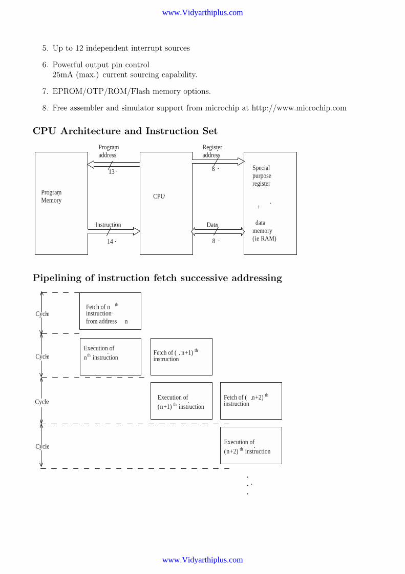
CPU Architecture and Instruction Set
ProgramMemory
CPU
Specialpurposeregister
+
datamemory(ie RAM)
Data
Programaddress
Instruction
14
13 8
8
Registeraddress
Pipelining of instruction fetch successive addressing
Fetch of n th
instructionfrom address n
Execution ofnth instruction
Fetch of ( n+1) th
instruction
Execution of(n+1) th instruction
Fetch of ( n+2) th
instruction
Execution of(n+2) th instruction
.
.
.
Cycle
Cycle
Cycle
Cycle
www.Vidyarthiplus.com
www.Vidyarthiplus.com
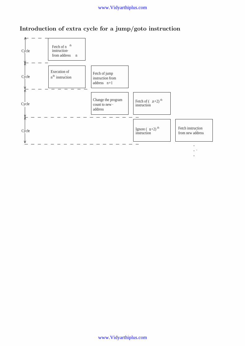
Introduction of extra cycle for a jump/goto instruction
Fetch of n th
instructionfrom address n
Execution ofnth instruction
Fetch of jumpinstruction fromaddress n+1
Change the programcount to newaddress
Fetch of ( n+2) th
instruction
Ignore ( n+2) th
instruction
.
.
.
Cycle
Cycle
Cycle
CycleFetch instructionfrom new address
www.Vidyarthiplus.com
www.Vidyarthiplus.com

Register File Structure and Addressing Modes
Register file → locations that an instruction can access via an address.Register file consists of two components.
1. General purpose register file (same as RAM)
2. Special purpose register file
7F
201F
00
RAM(96 bytes)
Special purposeRegister(32 bytes)
Bank 1128 bytes
RAM(32 bytes)
FF
C0BF
A09F
80
Extra 64bytes of RAM inPIC 16 C63 16 C65A 16 C73A 16 C74A
Special purposeRegister(32 bytes)
Bank 0128 bytes
RPO bit in the Status register detects the bank. 7 bit of direct address TRPO determines the absoluteaddress of the register.Indirect addressing modeFSR contains the 8-bit address of the data/register.
CPU Registers
W, the working register, is used by many instructions as the source of an operand. It may also serveas the destination for the result of the instructions execution. It works as the accumulator.
W working register
07
STATUS
7 6 5 4 3 2 1 0
0 0 RP0 NOT_TO NOT_PD Z DC C
(address 03H,83H)C = Carry bitDC = Digit Carry (same as AC, Auxiliary Carry)Z = Zero bitNOT-TO, NOT-PD→ Used in conjunction with PIC’s sleep modeRPO → register bank select bit used in conjunction with the direct addressing mode.
www.Vidyarthiplus.com
www.Vidyarthiplus.com

FSR
07
(address 04H,84H)Indirect data memory address points.FSR is the pointer used for indirect addressing.The program is supported by an eight-level stack. When an interrupt occurs, the program counteris automatically pushed on to the stack. Since PIC microcontrollers programs are normally designedfor handling one interrupt at a time, further
Basic Architecture of PIC Microcontroller
ProgramMemory
Program counter
Instruction RegisterAddress bus
InstructionDecoder &Control
FileRegisters
Databus
ALU
W
13
14
8
W → Temporary holding register, often called as an accumulator, cannot be accessed directly. Instead,contents must be moved to other registers that can be accessed directly.
www.Vidyarthiplus.com
www.Vidyarthiplus.com
Bank Addressing
Bank 0 Bank 1
00
01
02
03
04
05
06
07
08
09
0A
0B
0C
1F
80
81
82
83
84
85
8687
8889
8A
8B
9F
0FF07F
.
.
.
INDF
TMRO
PCL
STATUS
OPTION
FSR
PORTA TRISA
PORTB TRISB
PORTC TRISC
PORTD TRISD
PORTE TRISE
PCLATH
INTCON
INDF
PCL
STATUS
FSR
PCLATHINTCON
TRIS bit set → Post bit in I modeReset → Post bit in 0 mode.
EX: To set PORT B bit 0 as an output and loaded with a 1, PIC micro MCU code would exe-cute as:Port B. Bit = 1STATUS. RPO = 1TRIS B. Bit 0 = 0STATUS. RPO = 0
PIC 16C74A
Program Memory 4k(EPROM)×14Data Memory 192(Bytes)×8I/O Pins 33Parallel slave port YesA/D channel 8Serial Comm SPI/I2C,
USARTInterrupt sources 12
www.Vidyarthiplus.com
www.Vidyarthiplus.com

Memory Organization
The PIC 16C7X family has a 13-bit program counter capable of addressing 8k×14 program memory.PIC16C74A has 4k×14 program memory. For those devices with less than 8k program memory,accessing a location above the physically implemented address will cause a wraparound.
Program memory map and stack
16C74A has 4k program memory. The address range is 0000H - 0FFFH. The reset vector is 0000Hand the interrupt vector is 0004H.
.
.
.
.
.
.
PC <12 : 0 >
Stack level 1
Stack level 8
Reset Vector
Int . Vector
Page (0)
Page (1)
0000H
0004H0005H
07FFH0800H
0FFFH
www.Vidyarthiplus.com
www.Vidyarthiplus.com

LED Driver Example
+5V
10k Ω
0.1 µF
4 MHz Crystal
22 pF
6
8
8
5
R
Y
G
POR
TEPO
RTD
POR
TCPO
RTB
POR
TA
PIC 16C74A
VSS
OSC 1
OSC 2
22 pF
+5V
3
11
12
32
31
13
14
0
1
2
1
VDD
VDD
VSS
0.1 µF
PIC 16C74A has five ports. Each port is a bidirectional I/O port. In addition, they have the followingalternative functions.
Port Alternative uses of I/O pins
PORTA A/D Converter inputs ( PIC 16C7X parts)
PORTB External interrupt inouts
PORTC Serial port, Timer I/O
PORTD Parallel slave port
PORTE A/D Convertor inputs ( PIC 16C 7X )
I/O pins
Total I/O pins
Total pins
64A65A74A
62A63A73A
6 6
8
8 8
8
8
03
0
33 22
40/44 28
Port D alternative function is parallel slave port which enables one PIC microcontroller to be connectedto the data bus of another microprocessor. Since three LED’s are connected to three pins of Port Dto be used as normal I/O operation, the special alternative function is ruled out.
www.Vidyarthiplus.com
www.Vidyarthiplus.com

Structure of a port - pin of PIC microcontrolller
DTRIS
PORT
Pin write
Pin readData bus
Q
Q
D
TRIS register controls the direction of data flow.TRIS = 1 Sets the pin in the input mode.TRIS = 0 Sets the pin in the output mode.
; Toggle the green LED every half second.List P = PIC16C74A, F = INHX8M, C = 160, N = 80
ST = FF, MM = OFF, R = DECinclude ”C:\MPLAB\P16C74A.INC”- config ( CP OFF & PWRTE ON & XT-OSC & WDT OFF & BODEN OFF)error level -302
; EquatesBank0 RAM equ 20HMaxCount equ 50Green equ 0000000HBTenMsH equ 13TenMsL equ 250
; Variablescblock Bank0RAM ; Variables are declaredBLNKCNTCOUNTHCOUNTLendc
; Vectorsorg 000Hgoto Mainlineorg 004H
Stop:goto stop
Mainline:
www.Vidyarthiplus.com
www.Vidyarthiplus.com
call Initial ; InitializeMain loop:
call Blink ; Blink LEDcall TenMs ; Inset ten millisecond delay
indent goto Mainloop;Initial Subroutine
Initial:movlw MaxCount 0.5 secondmovwf BLNKCNT BLKCNT ← Nmovlw Greenmovwf PORTD PORTD ← Wbsf STATUS,RPO Set register access to bank 1clrf TRISD Set PORTD as O/P portbcf STATUS,RPO Set register access to bank 0return
; Blink Subroutine. This subroutine blinks a green LED in evey 0.5 secBlink:
decfsz BLNKCNT,F ; decrement loop counter and return if not zerogoto BlinkEndmovlw MaxCount ; Reinitialize BLNKCNTmovwf BLNKCNTmovlw GREEN w ← Green Toggle green LEDXorwf PORTD,F w ← Green Toggle green LED
Blink End;return
; Ten Ms subroutine (delay of 10ms)Ten Ms:
nopmovlw TenMsHmovwf COUNTH ; COUNTH ←wmovlw TenMsLmovwf COUNTL
TEN 1:decfsz CountL.fgoto Ten 1decfsz COUNTH,fgoto Ten 1return
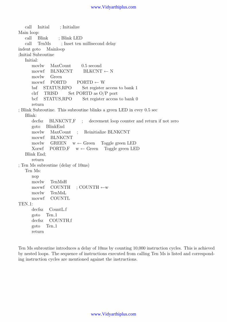
Ten Ms subroutine introduces a delay of 10ms by counting 10,000 instruction cycles. This is achievedby nested loops. The sequence of instructions executed from calling Ten Ms is listed and correspond-ing instruction cycles are mentioned against the instructions.
www.Vidyarthiplus.com
www.Vidyarthiplus.com
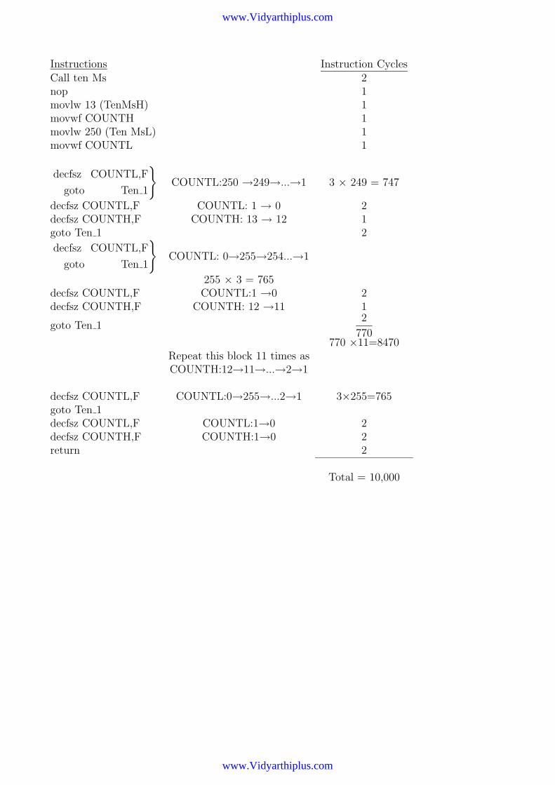
Instructions Instruction CyclesCall ten Ms 2nop 1movlw 13 (TenMsH) 1movwf COUNTH 1movlw 250 (Ten MsL) 1movwf COUNTL 1
decfsz COUNTL,F
goto Ten 1
COUNTL:250 →249→...→1 3 × 249 = 747
decfsz COUNTL,F COUNTL: 1 → 0 2decfsz COUNTH,F COUNTH: 13 → 12 1goto Ten 1 2
decfsz COUNTL,F
goto Ten 1
COUNTL: 0→255→254...→1
255 × 3 = 765decfsz COUNTL,F COUNTL:1 →0 2decfsz COUNTH,F COUNTH: 12 →11 1
goto Ten 12
770770 ×11=8470
Repeat this block 11 times asCOUNTH:12→11→...→2→1
decfsz COUNTL,F COUNTL:0→255→...2→1 3×255=765goto Ten 1decfsz COUNTL,F COUNTL:1→0 2decfsz COUNTH,F COUNTH:1→0 2return 2
Total = 10,000
www.Vidyarthiplus.com
www.Vidyarthiplus.com
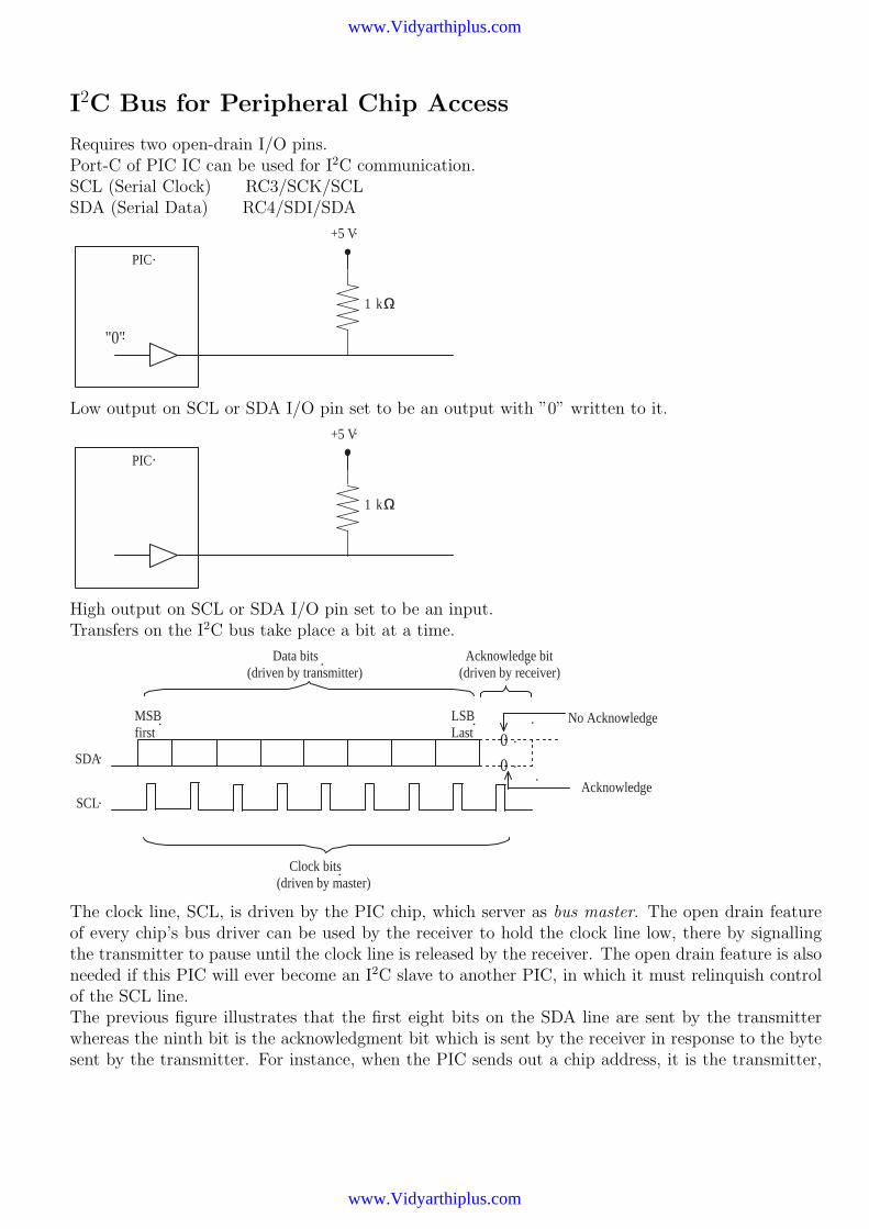
I2C Bus for Peripheral Chip Access
Requires two open-drain I/O pins.Port-C of PIC IC can be used for I2C communication.SCL (Serial Clock) RC3/SCK/SCLSDA (Serial Data) RC4/SDI/SDA
"0"
+5 V
1 kΩ
PIC
Low output on SCL or SDA I/O pin set to be an output with ”0” written to it.
+5 V
1 kΩ
PIC
High output on SCL or SDA I/O pin set to be an input.Transfers on the I2C bus take place a bit at a time.
SDA
SCL
MSBfirst
LSBLast
Data bits(driven by transmitter)
Acknowledge bit(driven by receiver)
No Acknowledge
Acknowledge
Clock bits(driven by master)
0
0
The clock line, SCL, is driven by the PIC chip, which server as bus master. The open drain featureof every chip’s bus driver can be used by the receiver to hold the clock line low, there by signallingthe transmitter to pause until the clock line is released by the receiver. The open drain feature is alsoneeded if this PIC will ever become an I2C slave to another PIC, in which it must relinquish controlof the SCL line.The previous figure illustrates that the first eight bits on the SDA line are sent by the transmitterwhereas the ninth bit is the acknowledgment bit which is sent by the receiver in response to the bytesent by the transmitter. For instance, when the PIC sends out a chip address, it is the transmitter,
www.Vidyarthiplus.com
www.Vidyarthiplus.com

while every other chip on the I2C bus is a receiver. During the acknowledgment bit time, the addressedchip is the only one that drives the SDA line, pulling it low in response to the masters pulse on SCL,acknowledging the reception of its chip address.When the data transfer direction is reversed that is form a peripheral chip to the PIC, which is themaster , the peripheral chip drives the eight daa bits in response to the clock pulse from PIC. In thiscase, the acknowledge bit is driven in a special way by the PIC, which is serving as receive but alsoas bus master. If the peripheral chip is one that can send the contents of successive internal addressback to the PIC, then PIC completes the reception of each byte and signals a request for the nextbyte by pulling SDA line low in acknowledgment. After any number of bytes have been received bythe master from the peripheral, the PIC can signal the peripheral to stop any further transfers by notpulling the SDA line low in acknowledgment.SDA line should be stable during high period of the clock (SCL). When the slave peripheral is drivingSDA line , either as transmiter or acknowledge, it initiates the new bit in response to the falling edgeof SCL, after a specified time. It maintains that bit on SDA line until the next falling edge of SCL,again afte r a specified hold time.I2C bus transfers consist of a number of byte transfers framed between a START condition and eitheranother START condition or a STOP condition. Both SDA and SCL lines are released by all drivesand float high when bus transfers are not taking place. The PIC (I2C bus controller) initiates atransfer with a START condition by first pulling SDA low and then pulling SCL as shown in thefigure.
SDA
SCL
START Condition STOP Condition
SDA
SCL
Similarly, the PIC terminates a multiple byte transfer with the STOP condition. With both SDA andSCL initially low, it first releases SCL and then SDA. Both then occurrences are easily recognized byI2C hardware in each peripheral chip since they both consist of a chage in SDA line which SCL ishigh, a condition that never happens in the middle of a byte transfer.
Data Communication protocol
In I2C communication standard, there is one bus master and several slaves. It can be assumed herethat the PIC microcontroller is the bus master and several peripheral devices connected to SDA andSCL bus are slaves.Following a start condition, the master sends a 7-bit address of the slave on SDA line. The MSBis sent first. After sending 7 bit address of the slave peripheral a R/W bit (8th bit) is sent by themaster. If R/W bit is 0 the following byte (after the acknowledgment) is written by the master to theaddressed slave peripheral. If R/W bit is 1, the following byte after the acknowledgment bit has tobe read from the slave by the master. After sending the 7-bit address of the slave, the master sendsthe address of the internal register of the salve where from the data has to be used or written to. Thesubsegment access is automatically directed to the next address of the internal register.
www.Vidyarthiplus.com
www.Vidyarthiplus.com

The following diagrams give the general format to write and read from several peripheral internalregisters.
STARTcondition 7-bit address
of peripheral chip
R/ W = 0for write Internal address N,
in peripheralData to be writteninto address N
WACK
SDA
S
Acknowledge byperipheral
Data to be writteninto address N+1
Data to be writteninto address N+2
STOPcondition
P
ACK
ACK
ACK
ACK
General format to write to several peripheral internal registers or addresses.
STARTcondition 7-bit address
of peripheral chip
R/W = 0for write Internal address N,
in peripheral Data readfrom address N
W
ACKS
Acknowledge byperipheral
Data read from address N +1
STOPcondition
P
ACK
ACK
NOACK
7-bit addressof peripheral chip
R
R/ N = 0for Read
No acknowledgment by PICsent out as a signalto terminate further transfers
General format to from several peripheral internal registers or addresses.
The 1995 I2C bus specification includes the timing constraints for older chips designed for a maximumbit rate of 100kbits/s. It also includes constraints for newer fast-mode 400kbits/s parts.
www.Vidyarthiplus.com
www.Vidyarthiplus.com

I2C Bus Subroutines:
I2C bus fast-mode timing constraints.
t STOP-START
SDA
SCL
STOPcondition
STARTcondition
t STOP t START
STOP - to - START Constraints
SDA
SCL
Acknowledge bitSTARTcondition
t LOWt START
t SETUP
Acknowledge bit to START (restart condition)
t START
SDA
SCL
data bit data bit
t SETUP t HOLD
t HIGH t LOW
Data bit to data bit
www.Vidyarthiplus.com
www.Vidyarthiplus.com
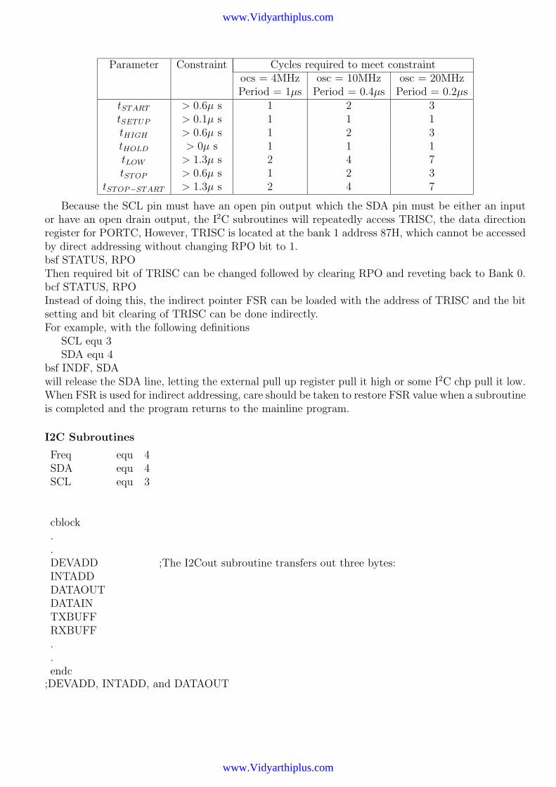
Parameter Constraint Cycles required to meet constraintocs = 4MHz osc = 10MHz osc = 20MHzPeriod = 1µs Period = 0.4µs Period = 0.2µs
tSTART > 0.6µ s 1 2 3tSETUP > 0.1µ s 1 1 1tHIGH > 0.6µ s 1 2 3tHOLD > 0µ s 1 1 1tLOW > 1.3µ s 2 4 7tSTOP > 0.6µ s 1 2 3
tSTOP−START > 1.3µ s 2 4 7
Because the SCL pin must have an open pin output which the SDA pin must be either an inputor have an open drain output, the I2C subroutines will repeatedly access TRISC, the data directionregister for PORTC, However, TRISC is located at the bank 1 address 87H, which cannot be accessedby direct addressing without changing RPO bit to 1.bsf STATUS, RPOThen required bit of TRISC can be changed followed by clearing RPO and reveting back to Bank 0.bcf STATUS, RPOInstead of doing this, the indirect pointer FSR can be loaded with the address of TRISC and the bitsetting and bit clearing of TRISC can be done indirectly.For example, with the following definitions
SCL equ 3SDA equ 4
bsf INDF, SDAwill release the SDA line, letting the external pull up register pull it high or some I2C chp pull it low.When FSR is used for indirect addressing, care should be taken to restore FSR value when a subroutineis completed and the program returns to the mainline program.
I2C Subroutines
Freq equ 4SDA equ 4SCL equ 3
cblock..DEVADDINTADDDATAOUTDATAINTXBUFFRXBUFF..endc
;The I2Cout subroutine transfers out three bytes:
;DEVADD, INTADD, and DATAOUT
www.Vidyarthiplus.com
www.Vidyarthiplus.com

I2C out :call startmovf DEVADD, W ; Send peripheral address with R/W=0 (write)Call Txmovf INTADD, WCall Txmovf DATAOUT, WCall TxCall Stop ; Generate Stop conditionreturn
; The I2C in subroutine transfers out DEVADD (with R/W=0); and INTADD, restarts, transfers out DEVADD (with R/W=1); and read one byte back into DATAIN.
I2C in:Call Start ; Generate start conditionmovf DEVADD, W ; Send peripheral address R/W=0 (write)Call Txmovf INTADD, W ; Send peripheral’s internal addressCall TxCall ReStart ; Re STARTmovf DEVADD ,W ; Send peripheral’s address.iorlw 0000000.1 B ; with R/W=1 (read)Call Txbsf TXBUFF, 7 ; NOACK the following reading of one byteCall Rx ; Read bytemovwf DATAIN ; inte DATAINCall stop ; Generate stop conditionreturn
; The start subroutine initializes the I2C bus and then; generates the START condition on the I2C bus; The ReStart entry point bypadd the initialization of the; I2C bus
Start:movlw 00111011 ; Enable I2C Master mode.movwf SSPCONbcf PORTC, SDA ; DRIVE SDA low when it is an outputbcf PORTC, SCL ; DRIVE SCL low when it is an outputmovlw TRISC ; Set indirect pointer to TRISCmovwf FSR
ReStart:bsf INDF, SDA ; Make sure SDA is high - I/P mode
www.Vidyarthiplus.com
www.Vidyarthiplus.com

bsf INDF ,SCL ; Make sure SCL is high - I/P modedelay 0,1,2 notbcf INDF ,SDA ; Make SDA lowdelay 0,1,2 nopbcf INDF, SCL ; Make SCL lowreturn
Stop:bcf INDF, SDA ; Return SDA lowbsf INDF, SCL ; Drive SCL highdelay 0,1,2bsf INDF, SDA ; and then drive SDA highreturn
; The Tx subroutine sends out the byte passed to it in W.; It returns with z = 1 if ACK occurs.; It returns with z = 0 if NOACK occurs.
Tx:movwf TXBUFFbsf STATUS, C
Tx 1:rlf TXBUFF, F ; rotate TXBUFF left, through carrymovf TXBUFF, F ; Set Z bit when all 8 bits have been transformedbtfss STATUS, Z ; until z = 1Call Bitout ; Send carry bit then clear carry bitbtfss STATUS, Zgoto TX 1Call Bit Inmovlw 00000001 BEnd wf RXBUFF, W ; z = 1 if ACK z = 0 if NOACKreturn
; The Rx subroutine receives a byte from I2C bus into W,; using RXBUFF buffer; Call Rx with bit 7 of TXBUFF clear for ACK; Call Rx with bit 7 of TXBUFF set for NOACK
Rx:movlw 00000001 Bmovwf RXBUFF
Rx 1:rlf RXBUFF, FCall Bit Inbtfss STATUS, C
www.Vidyarthiplus.com
www.Vidyarthiplus.com
goto Rx 1rlf TXBUFF, FCall BitOutmovf RXBUFF, Wreturn
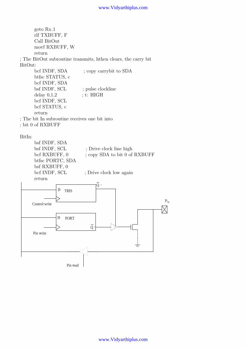
; The BitOut subroutine transmits, hthen clears, the carry bitBitOut:
bcf INDF, SDA ; copy carrybit to SDAbtfsc STATUS, cbcf INDF, SDAbsf INDF, SCL ; pulse clocklinedelay 0,1,2 ; t: HIGHbcf INDF, SCLbcf STATUS, creturn
; The bit In subroutine receives one bit into; bit 0 of RXBUFF
BitIn:bsf INDF, SDAbsf INDF, SCL ; Drive clock line highbcf RXBUFF, 0 ; copy SDA to bit 0 of RXBUFFbtfsc PORTC, SDAbsf RXBUFF, 0bcf INDF, SCL ; Drive clock low againreturn
Pin
D
TRIS
PORT
Control write
Pin write
Pin read
Q
QD
www.Vidyarthiplus.com
www.Vidyarthiplus.com
Examples of I2C bus Interfacing
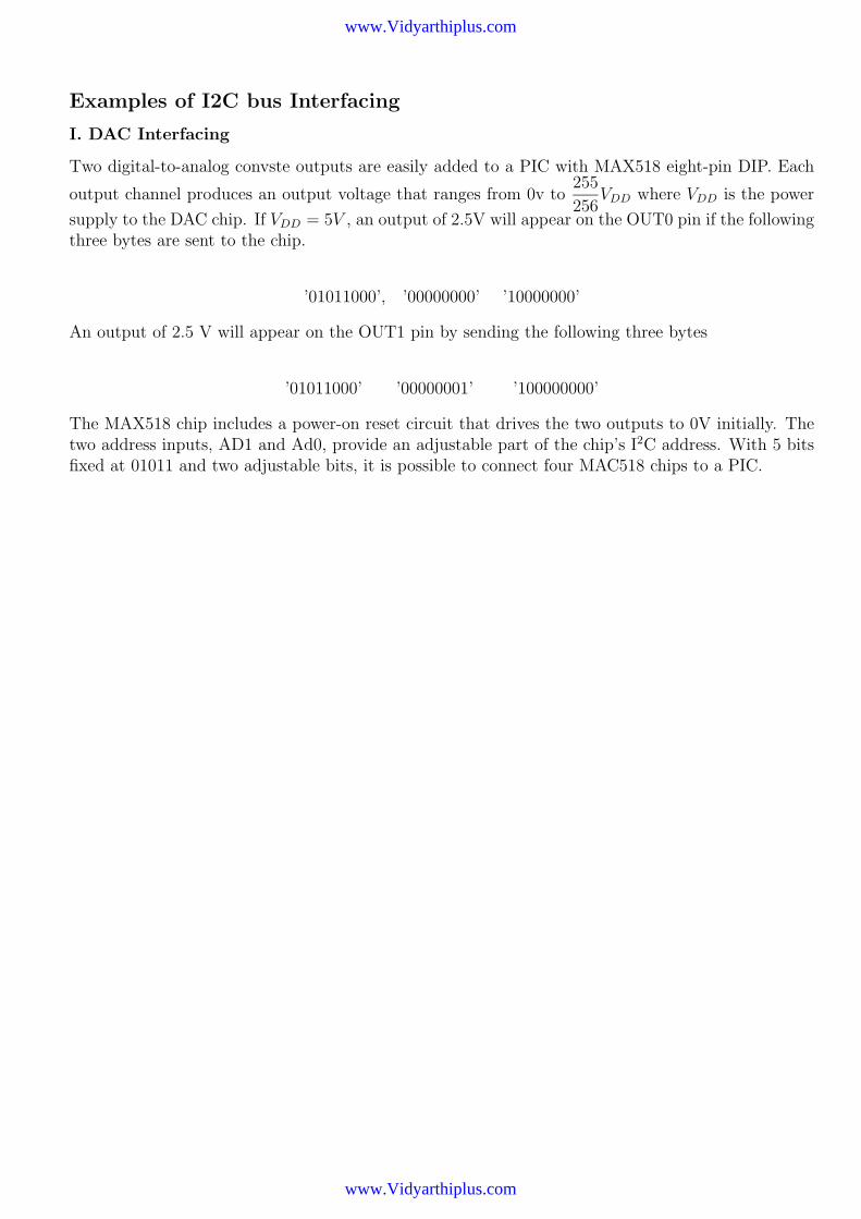
I. DAC Interfacing
Two digital-to-analog convste outputs are easily added to a PIC with MAX518 eight-pin DIP. Each
output channel produces an output voltage that ranges from 0v to255
256VDD where VDD is the power
supply to the DAC chip. If VDD = 5V , an output of 2.5V will appear on the OUT0 pin if the followingthree bytes are sent to the chip.
’01011000’, ’00000000’ ’10000000’
An output of 2.5 V will appear on the OUT1 pin by sending the following three bytes
’01011000’ ’00000001’ ’100000000’
The MAX518 chip includes a power-on reset circuit that drives the two outputs to 0V initially. Thetwo address inputs, AD1 and Ad0, provide an adjustable part of the chip’s I2C address. With 5 bitsfixed at 01011 and two adjustable bits, it is possible to connect four MAC518 chips to a PIC.
www.Vidyarthiplus.com
www.Vidyarthiplus.com
DAC Interfacing on I2C bus
PIC
RC4 /SD1 /SDA
RC3 /SCK /SCL
+5V
1kΩ
Analog outputs
8 1
4
3
SDA
SCL
7
5
6
2
0.1 µF
OUT1 OUT0
VDD
AD1AD0
MAX 518Dual 8-bit DAC
END
+5V
1kΩ
0 1 0 1 1 0 0 0
7-bit address
First byte ofmessage string
Write
AD0
AD1Match
0 0 0 00 0 0Second byte
1: Select OUT 1
0: Select OUT 0
1: Power-down mode ( 4µA, typical)
0: Normal DAC operation
1: Reset all DAC Registers
0: Normal DAC operation
Third byte
Analog output voltage =VDDB
256
www.Vidyarthiplus.com
www.Vidyarthiplus.com
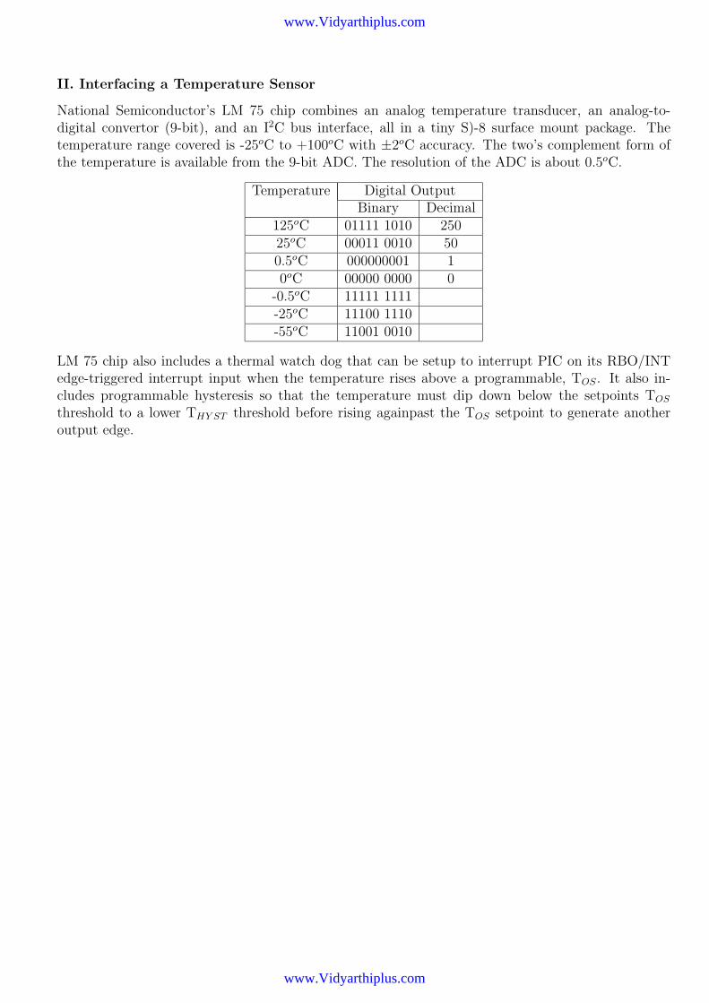
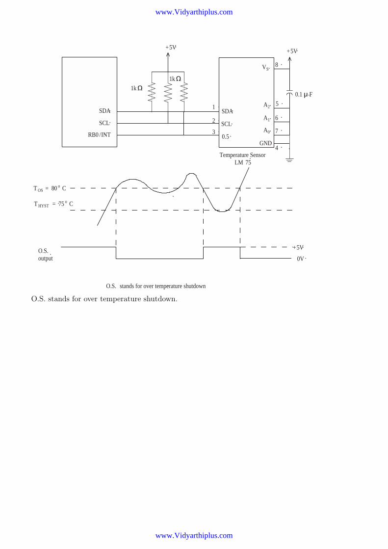
II. Interfacing a Temperature Sensor
National Semiconductor’s LM 75 chip combines an analog temperature transducer, an analog-to-digital convertor (9-bit), and an I2C bus interface, all in a tiny S)-8 surface mount package. Thetemperature range covered is -25oC to +100oC with ±2oC accuracy. The two’s complement form ofthe temperature is available from the 9-bit ADC. The resolution of the ADC is about 0.5oC.
Temperature Digital OutputBinary Decimal
125oC 01111 1010 25025oC 00011 0010 500.5oC 000000001 10oC 00000 0000 0
-0.5oC 11111 1111-25oC 11100 1110-55oC 11001 0010
LM 75 chip also includes a thermal watch dog that can be setup to interrupt PIC on its RBO/INTedge-triggered interrupt input when the temperature rises above a programmable, TOS. It also in-cludes programmable hysteresis so that the temperature must dip down below the setpoints TOS
threshold to a lower THY ST threshold before rising againpast the TOS setpoint to generate anotheroutput edge.
www.Vidyarthiplus.com
www.Vidyarthiplus.com
+5V+5V
SDA
SCL
RB0 /INT
1kΩ
1
2
3
4
5
6
7
8
0.1 µF
VS
A1
A2
A0
GND0.5
Temperature SensorLM 75
SDA
SCL
1kΩ
T OS = 80 o C
T HYST = 75 o C
O.S.output
O.S. stands for over temperature shutdown
+5V
0V
O.S. stands for over temperature shutdown.
www.Vidyarthiplus.com
www.Vidyarthiplus.com
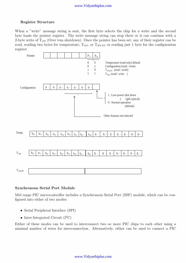
Register Structure
When a ”write” message string is sent, the first byte selects the chip for a write and the secondbyte loads the pointer register. The write message string can stop there or it can continue with a2-byte write of TOS (Over tem shutdown). Once the pointer has been set, any of their register can beread, reading two bytes for temperature, TOS, or THY ST or reading just 1 byte for the configurationregister.
P1 P0Pointer
0 00 11 01 1
Temperature (read only) defaultConfiguration (read / write)T HYST (read / write)T OS (read / write )
0 0 0 0 0 0
1 : Low-power shut down ( 1µA typical)0 : Normal operation (default)
Configuration
Other features not selected
0
b8 b7 b6 b5 b4 b3 b2 b1 b0 XXX X X X XTemp.
b8 b7 b6 b5 b4 b3 b2 b1 b0 XXX X X X XT OS
T HYST
Synchronous Serial Port Module
Mid range PIC microcontroller includes a Synchronous Serial Port (SSP) module, which can be con-figured into either of two modes:
• Serial Peripheral Interface (SPI)
• Inter-Integrated Circuit (I2C)
Either of these modes can be used to interconnect two oe more PIC chips to each other using aminimal number of wires for interconnection. Alternatively, either can be used to connect a PIC
www.Vidyarthiplus.com
www.Vidyarthiplus.com
chip to a peripheral chip. In this case of the I2C mode, the peripheral chip must also include an I2Cinterface. In contrast, the SPI mode provides the clock and serial data lines for direct connection toshift registers, adding an arbitrary number of I/O pins to a PIC chips.
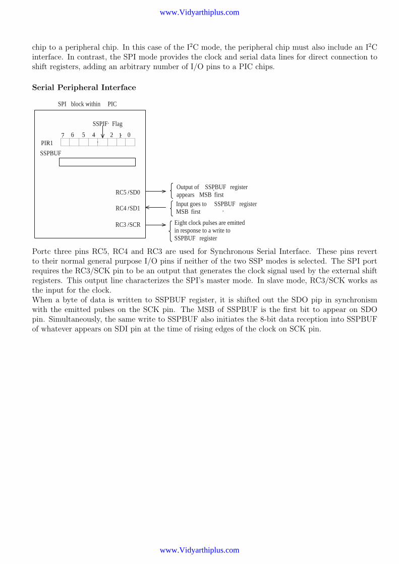
Serial Peripheral Interface
SPI block within PIC
PIR1
SSPBUF
RC5 /SD0
RC4 /SD1
RC3 /SCR
Output of SSPBUF registerappears MSB firstInput goes to SSPBUF registerMSB first
7 6 5 4
SSPIF Flag
2 1 0
Eight clock pulses are emittedin response to a write toSSPBUF register
Portc three pins RC5, RC4 and RC3 are used for Synchronous Serial Interface. These pins revertto their normal general purpose I/O pins if neither of the two SSP modes is selected. The SPI portrequires the RC3/SCK pin to be an output that generates the clock signal used by the external shiftregisters. This output line characterizes the SPI’s master mode. In slave mode, RC3/SCK works asthe input for the clock.When a byte of data is written to SSPBUF register, it is shifted out the SDO pip in synchronismwith the emitted pulses on the SCK pin. The MSB of SSPBUF is the first bit to appear on SDOpin. Simultaneously, the same write to SSPBUF also initiates the 8-bit data reception into SSPBUFof whatever appears on SDI pin at the time of rising edges of the clock on SCK pin.
www.Vidyarthiplus.com
www.Vidyarthiplus.com
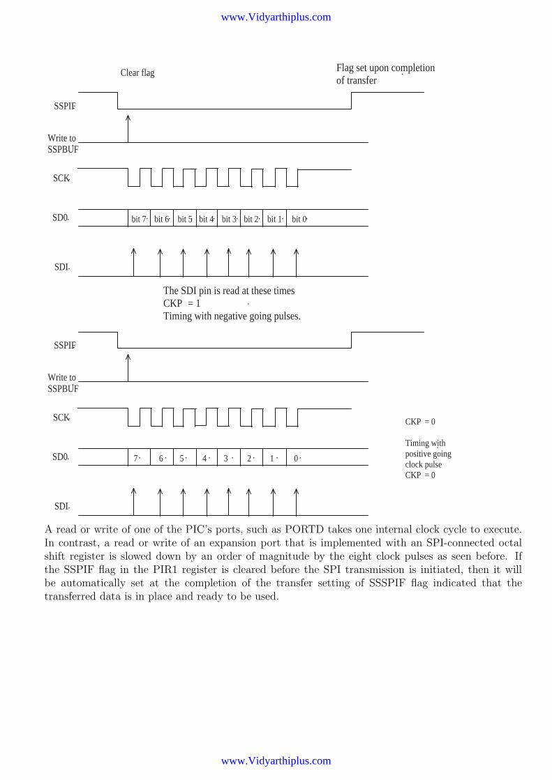
bit 7 bit 6 bit 5 bit 4 bit 3 bit 2 bit 1 bit 0
Clear flag
SSPIF
Write toSSPBUF
SCK
SD0
SDI
Flag set upon completionof transfer
The SDI pin is read at these timesCKP = 1Timing with negative going pulses.
7 6 5 4 3 2 1 0
SSPIF
Write toSSPBUF
SCK
SD0
SDI
CKP = 0
Timing withpositive goingclock pulseCKP = 0
A read or write of one of the PIC’s ports, such as PORTD takes one internal clock cycle to execute.In contrast, a read or write of an expansion port that is implemented with an SPI-connected octalshift register is slowed down by an order of magnitude by the eight clock pulses as seen before. Ifthe SSPIF flag in the PIR1 register is cleared before the SPI transmission is initiated, then it willbe automatically set at the completion of the transfer setting of SSSPIF flag indicated that thetransferred data is in place and ready to be used.
www.Vidyarthiplus.com
www.Vidyarthiplus.com

Output port expansion
b0 b1 b2 b3 b4 b5 b6 b7
Latch clock
Data in
Serial Clock
SPI
RC5 /SD0
RC4
RC3 /SCK
RD7
74HC595
D Q D Q D Q D Q D Q D Q D Q D Q
Vcc
+5V
Gnd
16
10
13
Port configurations
X 0 X XX 0 0 X
0 X X XX X X X
0 1 0 00 1 0 0
TRISC87H
TRISD85H
SSPCON14H
PIR1OCH
SSPBUF13H
Output for SCKGen purpose o/p to drive latchOutput for SDO
General purpose o/p to drive latch
SPI "master" mode withSCK = osc / 4
CKP = 1 : SCK will idle high
SSPEN = 1 : Enable Synchronous Serial Port ( SPI )
SSPIF = 1 When transfer iscomplete: clear beforebeginning of each transfer
www.Vidyarthiplus.com
www.Vidyarthiplus.com

Input port expansion
PICRD7
SPIRC4 /SDI
RC3 /SCK
MSB first
Data out
74HC165 Shift register
serial clock
LoadData in
b0 b1b2b3b4b5b6b7
RD7
SSPIF
Write toSSBUF toinitiate transfer
SCK ( CKP =0)
SDI
SPI readsinput bit here
Read SSPBUF
9 µs (for osc =4MHz )
bit 0 bit 7 bit 6 bit 5 bit 4 bit 3 bit 2 bit 1 bit 0
Timing diagram
www.Vidyarthiplus.com
www.Vidyarthiplus.com
Port configurations
0 1 X XX 1 0 X
X 1 X XX 1 0 X
0 1 0 00 0 0 0
TRISC87H
TRISD88H
SSPCON14H
Output for SCKInput for SDIGeneral purpose input(to preempt SD0 o/p)
Gen. purpose o/p to drive load input
SPI "master" with SCK = ocs /4
CKP = 0 : SK0 will idle low
SSPEN = 1 : enableSynchronous Serial Port ( SPI )
Analog-to-Digital Converter
Features (16C7X)
• Eight input channels
• An analog multiplexer
• A track and hold circuit for signal on the selected input channel
• Alternative clock sources for carrying out the conversion.
• An adjustable autonomous sampling rate.
• The choice of an internal or external ref. voltage.
• 8-bit conversion
• Interrupt response when conversion is completed.
www.Vidyarthiplus.com
www.Vidyarthiplus.com

Digitaloutput
FF
FE
FD
04
03
02
01
000
input/ voltage / VREF
2561
2562
2563
256253
256254
256255
Port A and Port E pins are used for analog inputs/ Reference voltage for ADC.Port A pinsRA0/AN0 - Can be used as analog input-0RA1/AN1 - Can be used as analog input-1RA2/AN2 - Can be used as analog input-2RA3/AN3/VREF - RA3 can be used as analog input 3 or analog reference voltageRA4/TOCKI - RA4 can be used as clock input to Timer-0RA5/SS/AN4 - RA5 can be used as analog input 4 or the slave select for the sync serial port
Port E pins
RE0/RD/AN5 - Can be used as analog input 5RE1/WR/AN6 - Can be used as analog input 6RE2/CS/AN7 - Can be used as analog input 7
PIC microcontroller has internal sample and hold circuit. The input signal should be stable acrossthe capacitor before the conversion is initiated
~
PIC
Other analoginput cahnnels
RSOURCE
VSOURCE
Samplingswitch
Switchresistance
Analogmultiplexer
VHOLD
to ADC
CHOLD
pF50≈
www.Vidyarthiplus.com
www.Vidyarthiplus.com

After waiting out the sampling time, a conversion can be initiated. The ADC circuit will open thesampling switch and carry out the conversion of the input voltage as it was at the moment of openingof the switch. Upon completion of the conversion, the sampling switch is closed and VHOLD againtracks VSOURCE.
Using the A/D Converter
Registers ADCON1, TRISA, and TRISE must be initialized to select the reference voltage and theinput channels. The first step selects the ADC clock source from among four choices (OSC/2, OSC/8,OSC/32, and RC). The constraint for selecting clock frequency is that the ADC clock period mustbe 1.6mus or greater.The A/D modules has three registers. These registers are
• A/D Result Register (ADRES)
• A/D Control Register 0 (ADCONO)
• A/D Control Register 1 (ADCON1)
The ADCONO register as shown here, controls the operation of A/D module.
7 6 5 4 3 2 1 0
ADCS1 ADCS0 CHS2 CHS1 GO/DONE AD ONCHS0
bit 7 - 6ADCS1 : ADCS 000 = Fosc/201 = Fosc/810 = Fosc/3211 = FRC (clock derived from an internal RC oscillator)
bit 5 - 3CHS2: CHS0000 - channel 0 - AN0001 - channel 1 - AN1010 - channel 2 - AN2011 - channel 3 - AN3100 - channel 4 - AN4101 - channel 5 - AN5110 - channel 6 - AN6111 - channel 7 - AN7
bit 2 A/D Conversion Status bitGO/DONE
if ADON = 11 = A/D conversion is in progress (setting this bit starts the A/D conversion)0 = A/D conversion is not in progress (this bit is automatically cleared by hardware when
www.Vidyarthiplus.com
www.Vidyarthiplus.com

A/D conversion is complete.)
bit 1Unimplemented
bit 0 ADON: A/D on bit1 = A/D converter module is ON0 = A/D converter module is OFF (not operating.)
ADCON1 Register
bit 7 bit 0
PCFG2 : PCFG0 : A/D Port Configuration Control bits
PCFG2 PCFG1 PCFG0
PCFG2 : PCFG0 : A/D Port Configuration Control bitsPCFG2 : PCFG0 RA0 RA1 RA2 RA5 RA3 RE0 RE1 RE2 VREF
000 A A A A A A A A VDD
001 A A A A VREF A A A RA3010 A A A A A D D D VDD
011 A A A A VREF D D D RA3100 A A D D A D D D VDD
101 A A D D VREF D D D RA311X D D D D D D D D -
7 6 5 4 3 2 1 0
X X X
Analog I/P
1: Digital I
0: Digital 0
1 : D/A I
0 : Digital 0
TRISA
TRISE
Disable Port Ealternate function
1: Analog / Digital input0:: Digital output
0 0 0 0
www.Vidyarthiplus.com
www.Vidyarthiplus.com
1. Configure A/D module
• Configure analog pins/ voltage reference/ and digital I/O (ADCON1)
• Select A/D channel (ADCON0)
• Select A/D conversion clock (ADCONO)
• Turn on A/D module (ADCONO)
2. Configure A/D interrupt (if required)
• Clear AD—F bit in PIR 1 reg
• Set AD—E bit in PIE 1 reg
• Set G—E bit
3. Wait for required acquisitiion time
4. Start conversion
• Set GO/DONE
5. Wait for A/D conversion to complete by either
• polling dor GO/DONE bit to be cleared
• waiting for the A/D interrupt
6. Read A/D result register (ADRES) Clear AD—F if required.
Example Program
A/D Conversion with Interrupt
bsf STATUS, RPO ; Select Bank1clrf ADCON 1 ; Configure A/D inputbsf PIE1, ADIE ; Enable A/D interruptbcf STATUS, RPO ; Select Bank 0movlw 0811+ ; Select fosc/32, channel 0, A/D on movwf ADCONObcf PIR1, ADIFbsf INTCON, PEIEbsf INTCON, GIE; Ensure that the required sampling time for the; selected input channel has elapsed.; Then the conversion may be started
bsf ADCONO, GO ; start A/D conversion; AD| F bit will be set; and GO/DONE bit is cleared; upon completion of A/D conversion
www.Vidyarthiplus.com
www.Vidyarthiplus.com

Code structure for large Programs
Memory paging is essential if the code exceeds 2k of program memory (2048). PIC 16C74A supports4096 addresses and hence it is important to consider memory paging for this processor.PCL and PCLATHThe program counter (PC) is 13-bit wide. The low byte comes from the PCL register, which isa readable and writable register. The upper bits (PC ¡12.8¿) are not readable, but are indirectlywritable through the PCLATH register. On any reset , the upper bits of the PC will be cleared.PCL← 0 and PCLATH ← 0. Two situations for loading the PC following any reset are given here.
1. Any write to PCL register load the content of PCL to lower 8 bit of PC and content of PCLATHto higher 5 bits.mov wf PCL
PC
12 8 7PCH PCL 0
85
PCLATH <4 : 0>
PCLATH
ALU
Instruction withPCL as adestination
2. PC is also loaded during a call or goto instruction
0 ≤ k ≤ 2047
Operation:k → PC < 10 : 0 >
PCLATH < 4 : 3 >→ PC < 12 : 11 >
Goto is an unconditional branch. The eleven bit immediate value is loaded into PC bits < 10 : 0 >.The upper bits of PC are loaded from PCLATH < 4 : 3 >.
PC
12 8 7PCH PCL
0
PCLATH <4 : 3>
PCLATH
11 10 9
11
Opcode <10 : 0>
Goto , CallInstruction
STACKThe PIC16CXX family has an 8 level deep X 13-bit wide hardware stack. The stack space is notpart of either program or data memory and the stack pointer is not readable or writable. The PCis pushed onto the stack when a CALL instruction is executed or an interrupt causes a branch. The
www.Vidyarthiplus.com
www.Vidyarthiplus.com

stack os POPed in the event of a RETURN, RETLW or a RETIE instruction execution. PCLATHis not affected by a PUSH or a POP operation. The stack operates on a circular buffer.Paging:Following any reset PCL and PCLATH are cleared to 0. For a 4k .... program memory, the addressrange is from 0000H to 0FFFH. Hence each call and goto instruction will actually reach the desiredaddress only if bit 3 of PCLATH is set or cleared correctly. However even for 4k PIC controllers, thereis no need to take care of PCLATH bit 3, if the code size fits into 2k address space. Bit 3 of PCLATHwill come out of reset in the zero state and there will never be a need to change it. Consequently,every call and goto instruction will go to the correct place.For large programs, it is helpful to break out blocks of code that are reached by a single call instructionand that terminates in a single return instruction. Such a block of code can be placed on programmemory’s page 1. Then, before executing the call instruction to reach the block, the following in-struction can be executed.
bsf PCLATH, 3 ; Switch to program memory’s Page 1.When it is finally time to exit from the block to return to the mainline program in Page 0, the returninstruction is preceded by the instruction
bcf PCLATH, 3
Program memory allocation for large programs
Page 0 Page 1Hex address000
004
Main line
7FF FFF
Block2
Block1
Int Service
Hex address800
Store W , STATUsPCLATH
bsf PCLATH , 3goto Int.Service
bsf PCLATH , 3 Call Block 1
bsf PCLATH , 3 Call Block 2
.
.
.
.
.
.
.
restore PCLATHSTATUS, W retie
bcf PCLATH , 3 return
bcf PCLATH , 3 return
.
.
.
www.Vidyarthiplus.com
www.Vidyarthiplus.com

Overview of Timer Modules
Timer-0 Overview
The Timer 0 module is a simple 8-bit overflow counter. The clock source can be either the internalclock (fosc/4) or an external clock. When the clock source is an external clock, the Timer-0 modulecan be selected to increment on either the rising or falling edge.Timer-0 module also has a programmable prescalar option. This prescalar can be assigned either toTimer 0 or the watchdog Timer.The counter sets a flag TOIF when it overflows and can cause an interrupt at that time if thatinterrupt source has been enabled (TOIF=1). Timer 0 can be assigned an 8-bit prescalar that candivide the input by 2,4,8,16,...,256. Writing to TMRO resets the prescalar assigned to it.Timer-0, or its prescalar can be connected to either of two input sources.
1. fosc/4
2. RA4/ TOCKI, the input connected to bit 4 of PORTA.
1: Prescaler assigned to watchdog timer0: Prescaler assigned to Timer 0
RBPU INTEDG 0 TOSE 1 PS2 PS1 PS0
PSA
TOCS1: Timer 0 Clock source is
RA4 /TOCK0: Timer 0 clock source is
f_osc / 4
TMRO 01H
8-bit counter f_osc / 4
Interrupt CPU
Other Int . Set
11 .INTCON0BH, 8BH
GIE : Global int . enable bit
TOIE : Timer 0 overflow
int . enable bit
TOIF : TMRO overflow
int . flag
2-cycle delay
www.Vidyarthiplus.com
www.Vidyarthiplus.com

Timer-0 use with prescalar
0 0 PS2 PS1 PS0
TOCS = 0, Timer 0 clock is f_osc / 4
PCA = 0, Prescaler assigned to Timer0
OPTION_ REG81H
0 0 0 20 0 1 40 1 0 80 1 1 161 0 0 321 0 1 641 1 0 1281 1 1 256
Prescaler .......
TMRO (01H) 2-cycle delay Presclar
fosc /4
Overflow
8 - bit counter
www.Vidyarthiplus.com
www.Vidyarthiplus.com

External clock synchronization
Q1 Q2 Q3 Q4 Q1 Q2 Q3 Q4 Q1 Q2 Q3 Q4 Q1 Q2 Q3 Q4
External clockInput or Prescaleroutput
External clock/Prescaler outputafter sampling
IncrementTimer0 ( Q4 )
Timer 0
Timer-1 Module
The Timer1 module is a 16-bit timer/counter consisting of two 8-bit registers (TMR1H and TMR1L)which are readable and writable. The TMR1 register pair (TMR1H: TMR1L) increments from 0000Hto FFFFH and rolls over to 0000H. The TMR1 interrupt, if enabled, is generated on overflow whichsets the interrupt flag bit TMR1IF-(PIR< 0 >). This interrupt can be enabled/disabled by set-ting/clearing TMR1 interrupt enable bit TMR1IE-(PIE < 0 >)The operating and control modes of Timer 1 is determined by the special purpose register T1CON.T1CON (10H)
www.Vidyarthiplus.com
www.Vidyarthiplus.com
0
Timer 1 Input clock Prescaleselect bits11 = 1:8 Prescale value10 = 1:4 Prescale value01 = 1:2 Prescale value00 = 1:2 Prescale value
Timer 1 ON bit0 = Stops Timer 11= Enables Timer 1
Timer 1 clock source select bit1 = External clock ( RCO /TIOSCO /T1CK1 )0 = Internal clock ( f_ocs / 4)
Timer 1 External clock Input Synchronization control bit
With TMR1CS = 1 1 = Donot synchrinize 0 = SynchronizeWith TMR1CS = 0 This bit is ignored.
Oscillator enable control bit 1 = oscillator is enabled 0 = oscillator is shut off
T1CKPS1 T10SCEN T1SYNC TMR1CS TMR1ON
bit 0bit 7
T1CKPS0
Set flag bitTMR1IF onoverflow
TMR1
TMR1H TMR1L
TMR1 ONon / off
T1SYNC
0
1
RCO /T1OSC /T1CK7
RC1 / T1OSI / CCP2
T1OSCEN
fosc /4
Internalclock
TMR1CS
1
0
Prescaler1,2,4,8
T1CKPS1 : T1CKPS0
Synchronize
SLEEP input
Enableoscillator
Timer 1 can operate in one of the two modes.
• As a timer. (TMR1CS = 0)In timer mode, Timer 1 increments in every instruction cycle. The Timer 1 clock source isfosc/4. Since the internal clock is selected, the timer is always synchronized and there is nofurther need of synchronization.
• As a counter (TMR1CS = 1)
www.Vidyarthiplus.com
www.Vidyarthiplus.com

In counter mode, external clock input from the pin RCO/T1OSC/T1CKI is selected.
Use of Timer-2
Timer 0: 8-bit timer/counter with 8-bit prescalarTimer 1: 16-bit timer/counter with prescalar, can be incremented during sleep
via external crystal/clock.Timer 2: 8-bit timer/counter with 8-bit period register, prescalar, post scalar.
Timer 2 Circuitry
Post Scaler AA=1,2,3,....15,16
Main Scaler BB=1,2,3,4,5,...255,256
PrescalerC
(C=1,4,16)
TMR2 8-bit resetable counter
Count
PR2
Set
equal
Reset Counter Count osc /4
8
compensatorPR2 : Period Register
PeripheralInterrupt Register
Interrupt CPU
TMR2IF
PIR10CH
TMR2IE
GIE PEIEbits 7 6 5 4 3 2 1 0
PIE 18CH
INTCON0BH / 8BH
1 1
bits 7 6 5 4 3 2 1 0
8
Timer 2 is an 8-bit timer with a prescalar and a port sclar. It can be used on the PWM modeof CCP modules. The TMR2 register is readable and writable and is cleared on any device reset.The input clock (fosc/4) has a prescalar option of 1:1, 1:4 or 1:16 selected by bits 0 and 1 of T2CONregister.The timer 2 module has a 8-bit period register (PR2). timer 2 increments from 00H until it matchesPR2 and then resets to 00H on the next increment cycle. PR2 is a readable and a writable register.PR2 is initialized to FFH on reset.The output of TMR2 goes through a 4-bit post scalar (1:1, 1:2 to 1:16) to generate a TMR2 interruptby setting TMR2IF flag.
www.Vidyarthiplus.com
www.Vidyarthiplus.com

T2CON12H
bits 7 6 5 4 3 2 1 0
Prescaler 00 C = 1 01 C = 4
1x C = 16
0 Disable TMR 21 Enable TMR 2
Post Scale0000 A = 10001 A = 2 . .1110 A = 151111 A = 16
CCP overview
The CCP module(s) can operate in one of the three modes: 16-bit capture, 16-bit compare, or upto1-bit Pulse Width Modulation (PWM).Capture mode captures the 16-bit value of TMR1 into CCPRxH: CCPRxL register pair. The captureevent can be programmed for either the falling edge, rising edge, fourth rising edge, or the sixteenthrising edge of the CCPx pair.Compare mode compares the TMR1H: TMR1L register pair to the CCPRxH: CCPRxL register pair.When a match occurs an interrupt can be generated, and the output pin CCPx can be forced to givenstate (High or Low), TMR1 can be reset (CCP1) or TMR1 reset and start A/D conversion (CCP2).This depends on the control bits < CCPxM3 : CCPxM0>PWM mode compares the TMR2 register to a 10 bit duty cycle register (CCPRxH : CCPRxL<5:4>)as well as an 8-bit period register (PR2). When the TMR2 register= Duty cycle register, the CCPxpin will be forcred low. When TMR2=PR2, TM2 is cleared to 00H, an interrupt can be generated,and the CCPx pin, if programmed in the O/P mode, will be forced high.
Compare Mode
Timer 1 is a 16-bit counter which can be used with CCP (Capture/compare/PWM) module to drivea pin high or low at precisely controlled time, independent of what the CPU is doing at that time.The pins are Port-C RC1/CCP2 and RC2/CCP1 pins.Which Timer1 includes a prescalar to divide the internal clock by 1,2,4 or 8, the choice of divide-by-one gives the finest resolution in setting the time of an output edge.
www.Vidyarthiplus.com
www.Vidyarthiplus.com
Capture/Compare/PWM modules
Each CCP (Capture/compare/PWM) module contains a 16-bit register which can operate as a 16-bitcapture register, as a 16-bit compare register or as a PWM master/slave duty cycle register. BothCCP1 and CCP2 are identical in operation, with the exception of the operation of the special eventtrigger.The following shows the CCP mode timer resources.
CCP Mode Timer ResourceCapture Timer 1Compare Timer 1PWM Timer 2
CCP1 Module:
Capture/Compare/PWM Register 1 consists of two 8-bit register: CCPR1L (low byte) and CCPR2H(high byte). THe CCP1CON register controls the operation of CCP1. All are readable and writable.
CCP2 Module:
Capture/Compare/PWM Register 2 consists of two 8-bit registers: CCPR2L (low byte) and CCPR2H(high byte). The CCP2CON register controls the operation of CCP2. Al are readable and writable.
CCP1CON Register / CCP2CON Register
bit 7 bit 0
CCPxX CCPxY CCPxM3 CCPxM2 CCPxM1 CCPxM0
bit 5-4: CCPxX : CCPxY : PWM Least Significant bits.Capture mode : UnusedCompare mode : UnusedPWM mode : These bits are the two LSBs of the PWM duty cycle. The eight MSBs are
found in CCPRxL.bit 3-0: CCPxM3 : CCPxM0 : CCPx Mode select bits.Capture Mode
RC2 / CCP 1 pin
Prescaler 1,4,16
Set flag bitCCP1IF
in PIR 1
CCPR1H CCPR1L
TMR1H TMR1L
www.Vidyarthiplus.com
www.Vidyarthiplus.com
Compare Mode
RC2 / CCP 1 CCPR1H CCPR1L
TMR1H TMR1L
Q S
R
TRISC < 2 >Output Enable
CCP1CON < 3.0 > Mode Select
Specialevent trigger
Set flag bit CCP1IFPIR 1 < 2 >
matchComparatorOutput
Logic
PWM Mode
In Pulse WIdth Modulation (PWM) mode, the CCPx pin produced upto a 10-bit resolution PWMoutput. Since CCP1 pin is multiplexed with PORT C data latch, the TRISC < 2 > pin must becleared to make CCP1 pin an output.Simplified PWM Block Diagram
CCPR1L
CCPR1H (slave)
TMR2
Comparator
PR2
Clear TimerCCP1 pin andlatch D.C.
R
S
Q
RC2 / CCP1
TRISC < 2 >
CCP1CON < 5 : 4 >
Comparator
PWM Output
www.Vidyarthiplus.com
www.Vidyarthiplus.com
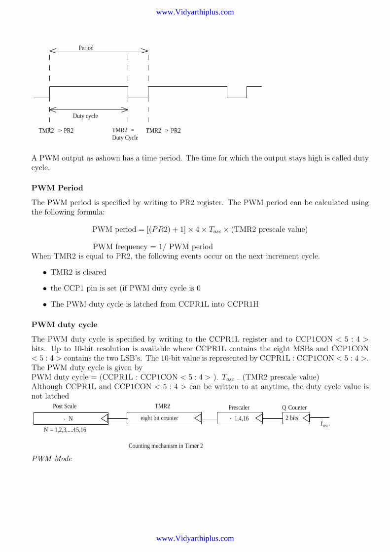
Period
Duty cycle
TMR2 = PR2 TMR2 = PR2TMR2 =Duty Cycle
A PWM output as ashown has a time period. The time for which the output stays high is called dutycycle.
PWM Period
The PWM period is specified by writing to PR2 register. The PWM period can be calculated usingthe following formula:
PWM period = [(PR2) + 1] × 4 × Tosc × (TMR2 prescale value)
PWM frequency = 1/ PWM periodWhen TMR2 is equal to PR2, the following events occur on the next increment cycle.
• TMR2 is cleared
• the CCP1 pin is set (if PWM duty cycle is 0
• The PWM duty cycle is latched from CCPR1L into CCPR1H
PWM duty cycle
The PWM duty cycle is specified by writing to the CCPR1L register and to CCP1CON < 5 : 4 >bits. Up to 10-bit resolution is available where CCPR1L contains the eight MSBs and CCP1CON< 5 : 4 > contains the two LSB’s. The 10-bit value is represented by CCPR1L : CCP1CON < 5 : 4 >.The PWM duty cycle is given byPWM duty cycle = (CCPR1L : CCP1CON < 5 : 4 > ). Tosc . (TMR2 prescale value)Although CCPR1L and CCP1CON < 5 : 4 > can be written to at anytime, the duty cycle value isnot latched
N
Post Scale
N = 1,2,3,....15,16
Counting mechanism in Timer 2
TMR2
eight bit counter
Prescaler
1,4,16
Q Counter
2 bitsfosc
PWM Mode
www.Vidyarthiplus.com
www.Vidyarthiplus.com

ten bit counter
ten bit counter
ten bit counter
TMR 2
8 - bit
Q - counter
2 - bits
Prescaler set to divide by one
fosc
Prescaler programed to divide by four
PrescalerUpper two bits Lower two bits
8 - bit
8 - bit 2 - bits 2 - bits
2 - bits 2 - bits 2 - bits
TMR 2
TMR 2
Q - counter
Q - counter
Prescaler
into CCPR1H until a match between PR2 and TMR2 occurs. In PWM mode, CCPR1H is a read-onlyregister.The CCPR1H register and a 2-bit internal latch are used to double buffer the PWM duty cycle. Thisdouble buffering is essential for glitchless PWM operation. When the CCPR1H and 2-bit latch matchTMR2 concatenated with an internal 2-bit Q clock or 2-bits of prescalar, the CCP1 pin is cleared.Maximum PWM resolution (bits) for a given PWM frequency can be calculated as
log( fosc
fPNM)
log2
If the PWM duty cycle is longer than the PWM period, then the CCP1 pin will not be cleared.
PWM Period and duty cycle calculation
Example Desired PWM frequency = 78.125 kHzfosc = 20MHzTMR2 Prescalar = 1
1
78.125 × 103= (PR2 + 1)4 × 1
20 × 106PR2 = 63
Find the maximum resolution of duty cycle that can be used with a 78.124 kHz frequency and 20MHz oscillator.
1
78.125 × 103= 2PWM Resolution.
1
20 × 106.1
256 = 2PWM Resolution
PWM Resolution = 8At most, an 8-bit resolution duty cycle can be obtained from a 78.125 kHz frequency and 20 MHzoscillator, ie, 0 ≤ CCPR1L : CCP1CON < 5 : 4 >≤ 255. Any value greater than 255 will result in a100 o/o duty cycle. The following table gives the PWM frequency fPWM if fosc=20MHz
www.Vidyarthiplus.com
www.Vidyarthiplus.com

Duty cycle resolution 10-bit counter scale PR2 value Prescalar 1 Prescalar 4 Prescalar 1610 bit 1024 255 19.53 KHz 4.88 kHz 1.22 kHz
≈ 10 bit 1000 249 20kHz 5kHz 1.25kHz8 bit 256 63 78.125kHz 19.53kHz 4.88kHz6 bit 64 15 312.5kHz 78.125kHz 19.53kHz
Interrupt Logic
GIE TOIETOIF
INTEINTFRBIERBIF
PEIE
RBO / INT
TMR2IETMR2IF
PSPIEPSPIF
ADIEADIF
RCIERCIF
TXIETXIF
SSPIESSPIF
CCP1IECCP1IF
CCP2IECCP2IF
TMR1IETMR1IF
PeripheralInterrupts
Four of PORTB’s pins RB7 : RB4 have an interrupt on change feature. Only pins configured oninputs can cause this interrupt to occur. The input pins (of RB7 : RB4) are compared with the oldvalues on the last read of Port B. the ”mismatch” outputs of RB7 : RB4 are used together to generatethe RB port change interrupt flag bit RB1F.
www.Vidyarthiplus.com
www.Vidyarthiplus.com