pipelined adc - tjprc. pipelined adc.full.pdf · pipelined adc and also the critical block or the...
TRANSCRIPT

PIPELINED ADC
B VISHNU MOHAN & M SAI KRISHNA SHANKAR
Department of Electronics and Communication Engineering, Osmania University, Hyderabad, Andhra Pradesh, India
ABSTRACT
As the time is progressing the world is digitalizing (from Tape recorders to DVD’s, Analog speedometer to
Digital speedometer ….etc). This is because digital systems are easy to build and digital signals are easy to process and
circuit is less complex, but the importance of analog prevails. Because what we hear, speak and see is analog by nature.
So we can’t understand digital signals and Digital systems do not understand analog signals. So we need an interface
between Analog and Digital worlds, where our interest and the basis of our project lies, that is on “ANALOG TO
DIGITAL CONVERTER”. There are various types of ADCs available. Among them FLASH type is the fastest. But it
requires more hardware. The PIPELINED ADC is an architecture for data conversion which uses the concept of pipelining
to reduce the hardware in the FLASH type ADC and maintaining the speed comparable to that of FLASH type.
The resolution of pipelined ADC is high and comparable to that of SIGMA-DELTA. An excellent trade-off between
hardware and number of stages enable us to design a high speed low hardware ADC.
KEYWORDS: Analog to Digital Converter, Operational Trans Conductance Amplifier, Design of All the Blocks Used
in Pipeline
INTRODUCTION
This project report presents the design of 12-bit pipeline ADC operating at sampling rate of 100MHz. Pipelined
ADC with 2.5 bits/stage has been chosen as the architecture that meets given specifications. The circuit has been divided
into 6 stages of which all the odd stages operate on phy1 (Ф1) clock and even stages on phy2 (Ф2), which have been
derived from the single clock from a clock generator circuit.
In the pipelined ADC, Op-amp is the central component. In this project, gain boosted OTA has been studied and
implimented. From the specifications of the ADC, specifications of OTA are derived and the Gain Boosted Telescopic
OTA has been chosen as the OTA architecture that meets desired specifications.
Several blocks in a single stage of pipeline ADC include sub-ADC, Sub-DAC and Gain stage. In pipeline ADC,
Digital Error Correction Circuit is used to correct the errors due to comparator offsets and the interstage amplifier errors.
The design of all the blocks used in pipeline ADC are clearly explained and the simulation results have been shown.
In design procedure of OTA (operational transconductance amplifier) and Gain boosted Op-amp are studied.
While designing , an OTA of 56.7db gain and Unity Gain Frequency around 9.2GHz is obtained. Inclusion of auxiliary
amplifiers boosted the gain of OTA to 102.345db. A basic 2.5bits/stage ADC is designed first. Integration of six such
stages along with Shift Registers and Digital Error Correction Circuit forms a 12-bit HIGH SPEED PIPELINED ADC.
DESIGN OF DIFFERENT BLOCKS USED IN PIPELINED ADC
This chapter describes the design of various blocks used in pipelined ADC such as Clock Generator, Sub-ADC,
MDAC or Gain stage and Sub-DAC. All the blocks are simulated individually AT 100 M-Hz and the results are shown.
International Journal of Electronics,
Communication & Instrumentation Engineering
Research and Development (IJECIERD)
ISSN(P): 2249-684X; ISSN(E): 2249-7951
Vol. 3, Issue 5, 2013, Dec 2013, 61-74
© TJPRC Pvt. Ltd.
62 B Vishnu Mohan & M Sai Krishna Shankar
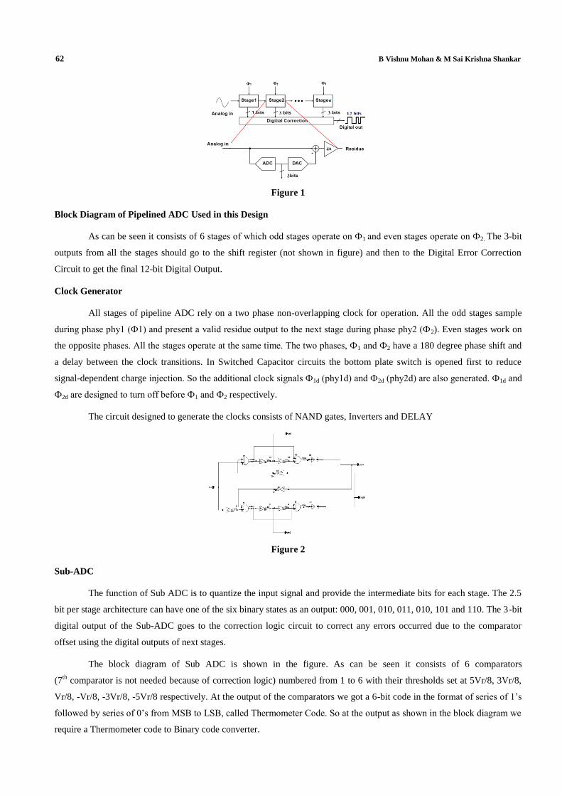
Figure 1
Block Diagram of Pipelined ADC Used in this Design
As can be seen it consists of 6 stages of which odd stages operate on Ф1 and even stages operate on Ф2. The 3-bit
outputs from all the stages should go to the shift register (not shown in figure) and then to the Digital Error Correction
Circuit to get the final 12-bit Digital Output.
Clock Generator
All stages of pipeline ADC rely on a two phase non-overlapping clock for operation. All the odd stages sample
during phase phy1 (Ф1) and present a valid residue output to the next stage during phase phy2 (Ф2). Even stages work on
the opposite phases. All the stages operate at the same time. The two phases, Ф1 and Ф2 have a 180 degree phase shift and
a delay between the clock transitions. In Switched Capacitor circuits the bottom plate switch is opened first to reduce
signal-dependent charge injection. So the additional clock signals Ф1d (phy1d) and Ф2d (phy2d) are also generated. Ф1d and
Ф2d are designed to turn off before Ф1 and Ф2 respectively.
The circuit designed to generate the clocks consists of NAND gates, Inverters and DELAY
Figure 2
Sub-ADC
The function of Sub ADC is to quantize the input signal and provide the intermediate bits for each stage. The 2.5
bit per stage architecture can have one of the six binary states as an output: 000, 001, 010, 011, 010, 101 and 110. The 3-bit
digital output of the Sub-ADC goes to the correction logic circuit to correct any errors occurred due to the comparator
offset using the digital outputs of next stages.
The block diagram of Sub ADC is shown in the figure. As can be seen it consists of 6 comparators
(7th
comparator is not needed because of correction logic) numbered from 1 to 6 with their thresholds set at 5Vr/8, 3Vr/8,
Vr/8, -Vr/8, -3Vr/8, -5Vr/8 respectively. At the output of the comparators we got a 6-bit code in the format of series of 1’s
followed by series of 0’s from MSB to LSB, called Thermometer Code. So at the output as shown in the block diagram we
require a Thermometer code to Binary code converter.

Pipelined ADC 63
Figure 3: Block Diagram of Sub-ADC
Table shows the outputs of the comparator and the 3-bit digital output for the all possible combinations of
differential input range (from –Vref to +Vref). In this design it is from -0.5V to +0.5V. So the comparator thresholds from 1st
comparator to 6th
comparator are 312.5mV, 187.5mV, 62.5mV, -62.5mV, -187.5mV and -312.5mV.
Table 1: Input/Output Table of Sub-ADC
Differential Input Sub-ADC
Output B2 B1 B0
Vin<-5Vr/8 000000 0 0 0
-5Vr/8<Vin<-3Vr/8 000001 0 0 1
-3Vr/8<Vin<-Vr/8 000011 0 1 0
-Vr/8<Vin<Vr/8 000111 0 1 1
Vr/8<Vin<3Vr/8 001111 1 0 0
3Vr/8<Vin<5Vr/8 011111 1 0 1
Vin>5Vr/8 111111 1 1 0
Comparator
As already discussed in section, dynamic latched comparators have been used to reduce the power dissipation.
Although the offset error is high, it can be taken care by the Digital Error Correction circuit. The circuit diagram of the
dynamic latched type comparator is shown in the figure.
W/Ls of the input and reference transistors for all the comparators are shown in the below Table.
Table 2
Comparator Input Transistor (µ/ µ) Reference Transistor (µ/ µ)
Comparator 1 10/0.18 6.25/0.18
Comparator 2 10/0.18 3.75/0.18
Comparator 3 10/0.18 1.25/0.18
When latchbar in the circuit is 0 the outputs are precharged to 3.3V. Now if latchbar is 1 the output of the
comparator is according to the input at which latchbar signal takes transition from 0 to 1. If that input is greater than
threshold of the comparator it remains at 3.3V only i.e., output is logic1; if input is less then output signal takes a transition
from 3.3 V to 0 i.e., logic 1 to logic 0.
Here the comparators output will go to the thermometer to binary code converter shown in figure. So the
comparators must be able to drive the load capacitance (sum of the drain capacitances of comparator and the input
capacitance of code converter). But actually here they are not able to drive in this design, so that buffers have been used at
the output of the comparators.

64 B Vishnu Mohan & M Sai Krishna Shankar
Figure 4: Thermometer to Binary Code Converter
Table shows the thermometer code values and their respective binary codes. From this using k-map logic for B2,
B1 and B0 is derived and the circuit shown above is designed. In this circuit AND gates are used at the starting to make
output Logic’0’ when latch is 0 and output is valid during latch is high.
Figure 5
Figure 6
The above figure shows the test bench and simulated results of Thermometer to bcd converter. From the table for
the input 011111 the output should be obtained as 101.The same is obtained here in the above table.
Figure 7

Pipelined ADC 65
The complete schematic of sub-ADC is shown in the above figure with Clocks. The latch signal shown in
thermometer to binary converter is not the same signal that has applied to the comparator. It clearly shows that it is delayed
clock with respect to latch. The comparators output will take some time to settle to the 0 values from 3.3V, so the signal
OE (output Enable) is a delayed one
MDAC
This example illustrates one way of implementing the MDAC and residue amplifier, a major component of the
pipelined ADC and also the critical block or the main block. As we know for a 2.5 bit stage, the residue amplifier has a
gain of four. The function of this circuit is threefold; to sample and hold the input signal, to generate a residue that is the
difference between the input and some reference, and to amplify this residue.
In this approach, the circuit operates on two phases, a sampling phase and a hold phase. During the sampling
phase shown in figure 8a, the input signal is sampled onto the capacitors C1 and C2. During the hold phase the capacitors
are then switched to one of seven voltages, +Vref, +2Vref/3, +Vref/3, 0, -Vref/3, -2Vref/3, -Vref. The voltage is chosen based
on the digital output of the analog to digital converter block (Sub ADC).
As the voltage is switched, the input voltage to the high gain amplifier, also known as the summing node voltage,
tends to change. As it does, the output of the high gain amplifier changes a great deal. The negative feedback through the
capacitor CF drives this summing node voltage to zero. The result is that the charge initially stored on capacitors C1 and
C2 is transferred to the capacitor CF.
Figure 8: (a) Sampling Phase (b) Hold Phase
Operation of Switched Capacitor Sample/Hold
Sub-DAC
The function of the Sub-DAC is to convert the intermediate digital outputs available at every stage into its
equivalent analog output that has to be subtracted from the input and passes this residue to the next stage for the
conversion.
The Block Diagram of the Sub DAC is shown below. As can be seen it consists of two blocks, one is a DAC
encoder and the other is a capacitive circuit.
Figure 9: Block Diagram of Sub-DAC
66 B Vishnu Mohan & M Sai Krishna Shankar
Inputs for the Sub DAC are the output of Sub ADC (B2, B1, B0), reference voltage (Vref) and Reset Signal (RST).
Output of ADC is a 3-bit binary number ranging from 000 to 110. Here in Sub DAC I have encoded them into another
sequence as shown in below table. The reason for encoding the ADC output into another sequence is, if we carefully
examine the table, for the case of 011 the output of Sub-DAC must be 0. So I have encoded the sequence such that the
output is 0 for the input of 000. Similarly if we observe the other codes and their outputs, we can say the outputs of DAC
are same for the codes above 011 and below 011 except the sign of the output. So in the encoded sequence I have used the
MSB bit C2 for the sign bit and the remaining bits C1 and C0 to get the required DAC output.
Input/Output Table of Sub-DAC
Table 3
Actual DAC
Input B2 B1 B0
Encoded Sequence
C2 C1 C0
DAC
Output
1 1 0 1 1 1 Vr
1 0 1 1 1 0 2Vr/3
1 0 0 1 0 1 Vr/3
0 1 1 0 0 0 0
0 1 0 0 0 1 -Vr/3
0 0 1 0 1 0 -2Vr/3
0 0 0 0 1 1 -Vr
In this design Vr is chosen as 0.5V. So DAC outputs become 500mV, 333.3mV, 166.7mV, 0, -166.7mV,
-333.3mV and -500mV for the encoded sequence of 111, 110, 101, 000, 001, 010 and 011 respectively.
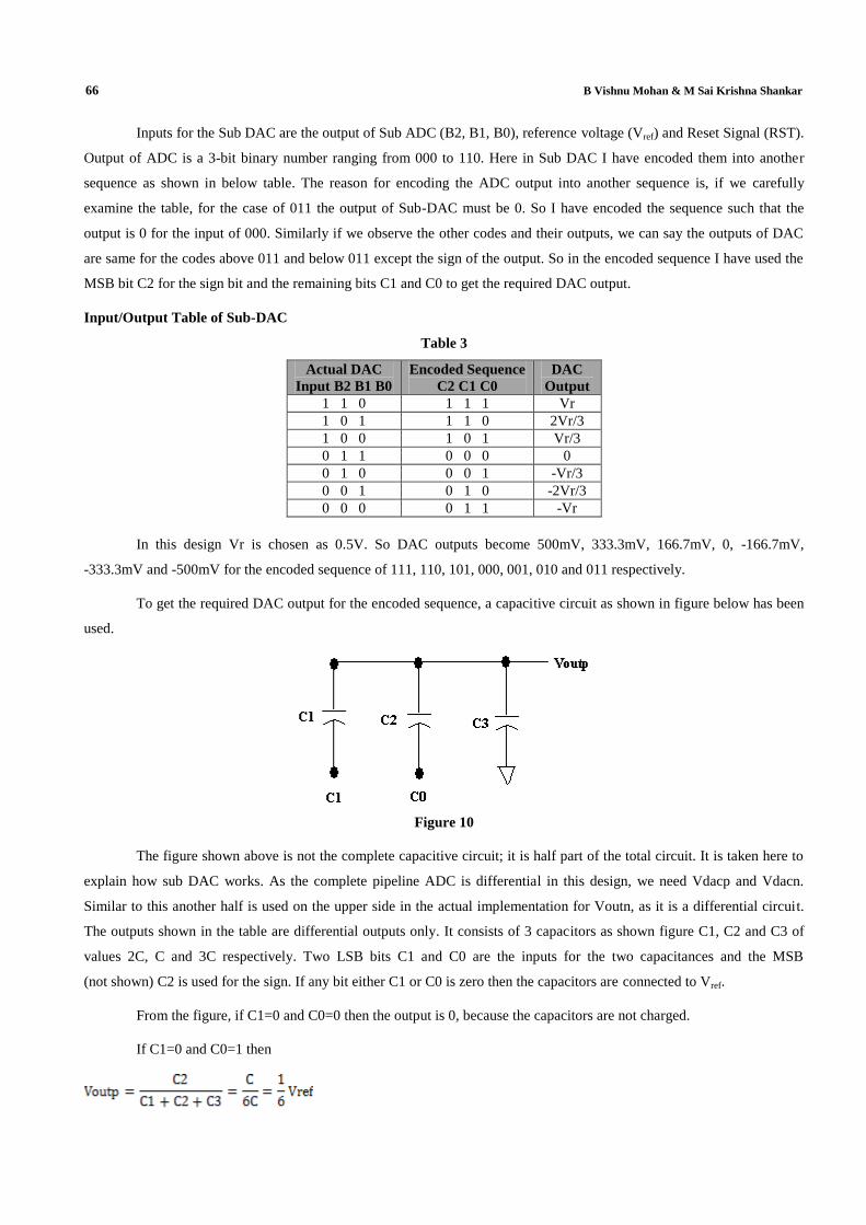
To get the required DAC output for the encoded sequence, a capacitive circuit as shown in figure below has been
used.
Figure 10
The figure shown above is not the complete capacitive circuit; it is half part of the total circuit. It is taken here to
explain how sub DAC works. As the complete pipeline ADC is differential in this design, we need Vdacp and Vdacn.
Similar to this another half is used on the upper side in the actual implementation for Voutn, as it is a differential circuit.
The outputs shown in the table are differential outputs only. It consists of 3 capacitors as shown figure C1, C2 and C3 of
values 2C, C and 3C respectively. Two LSB bits C1 and C0 are the inputs for the two capacitances and the MSB
(not shown) C2 is used for the sign. If any bit either C1 or C0 is zero then the capacitors are connected to Vref.
From the figure, if C1=0 and C0=0 then the output is 0, because the capacitors are not charged.
If C1=0 and C0=1 then
Pipelined ADC 67
Similarly , It implies
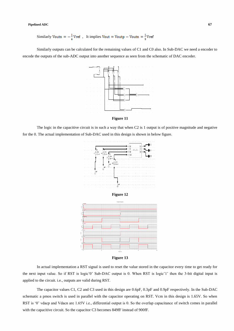
Similarly outputs can be calculated for the remaining values of C1 and C0 also. In Sub-DAC we need a encoder to
encode the outputs of the sub-ADC output into another sequence as seen from the schematic of DAC encoder.
Figure 11
The logic in the capacitive circuit is in such a way that when C2 is 1 output is of positive magnitude and negative
for the 0. The actual implementation of Sub-DAC used in this design is shown in below figure.
Figure 12
Figure 13
In actual implementation a RST signal is used to reset the value stored in the capacitor every time to get ready for
the next input value. So if RST is logic’0’ Sub-DAC output is 0. When RST is logic’1’ then the 3-bit digital input is
applied to the circuit. i.e., outputs are valid during RST.
The capacitor values C1, C2 and C3 used in this design are 0.6pF, 0.3pF and 0.9pF respectively. In the Sub-DAC
schematic a pmos switch is used in parallel with the capacitor operating on RST. Vcm in this design is 1.65V. So when
RST is ‘0’ vdacp and Vdacn are 1.65V i.e., differential output is 0. So the overlap capacitance of switch comes in parallel
with the capacitive circuit. So the capacitor C3 becomes 849fF instead of 900fF.

68 B Vishnu Mohan & M Sai Krishna Shankar
The simulated results of Sub-DAC were shown for the input of 101. As shown if RST is 0, output is zero and if
RST is 1, output is valid. RST signal here is operated at 100MHz.
Buffer Design
In the design at various places buffers are used to increase the drive capability. The basic design of the buffer has
been taken from [8]. It is basically an even no. of inverters kept in series with increasing aspect ratios (W/Ls).
Figure 14
A simple buffer is shown in the above figure. The sizes are different as it depends on the drive capability.
Figure 15
Schematics of Gates Used in Design
Schematic of AND Gate
Figure 16
Pipelined ADC 69
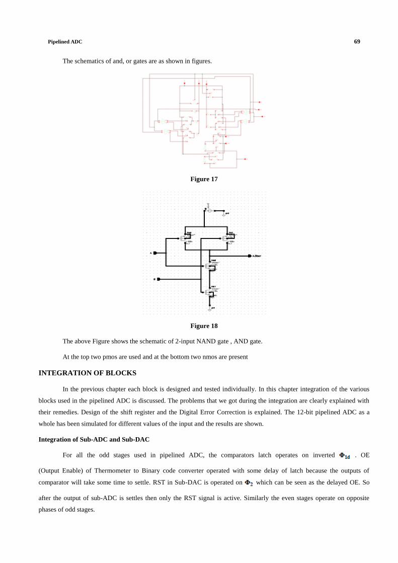
The schematics of and, or gates are as shown in figures.
Figure 17
Figure 18
The above Figure shows the schematic of 2-input NAND gate , AND gate.
At the top two pmos are used and at the bottom two nmos are present
INTEGRATION OF BLOCKS
In the previous chapter each block is designed and tested individually. In this chapter integration of the various
blocks used in the pipelined ADC is discussed. The problems that we got during the integration are clearly explained with
their remedies. Design of the shift register and the Digital Error Correction is explained. The 12-bit pipelined ADC as a
whole has been simulated for different values of the input and the results are shown.
Integration of Sub-ADC and Sub-DAC
For all the odd stages used in pipelined ADC, the comparators latch operates on inverted . OE
(Output Enable) of Thermometer to Binary code converter operated with some delay of latch because the outputs of
comparator will take some time to settle. RST in Sub-DAC is operated on which can be seen as the delayed OE. So
after the output of sub-ADC is settles then only the RST signal is active. Similarly the even stages operate on opposite
phases of odd stages.

70 B Vishnu Mohan & M Sai Krishna Shankar
Integration of Sub-DAC and MDAC
In the previous chapter the design of Sub-DAC and MDAC are discussed and they are simulated individually and
are working properly at 100M-Hz. But when we integrate the both with the same capacitor values we didn’t get the
required output. It is an interesting problem called the charge sharing. It implies at the output of Sub-DAC we have some
capacitance and at the input of MDAC also capacitors are there; so charge has been shared between them.
It is clearly explained now: During the capacitors C1 at the MDAC are charged to the input voltage and
during , C1 at MDAC is connected to the output of Sub-DAC. So here the charge stored on the capacitor C1 has been
shared between C1 and the output capacitance of Sub-DAC. To take care of this problem here a formula has been derived
for the capacitor values. Let is the capacitor at the input of MDAC, is the feedback capacitor of MDAC and is the
total capacitance at the output of Sub-DAC.
Initially both and charged to during . During , has been connected to the . So the charge
stored on the capacitor has been shared with .
i.e.,
Here is the voltage on and after charge sharing.
So the charge on becomes
During Ф1, C2 is charged to Vin. We require another 3Vin so that output is 4Vin for the digital input of
000.
From the above Eq ,
The 2nd
term in the above equation comes into picture due to charge sharing only. The actual capacitance for ,
and when simulated individually are 0.9pF, 0.3pF and 1.8pF respectively. But when they are integrated becomes
Here is the sum of the 3 capacitors used in the Sub-DAC. The 3 capacitors in Sub-DAC are also varied such
that we got the required output. They become 604.9fF, 302.4fF and 841.2fF instead of 600fF, 300fF and 849fF
respectively. By combining the Sub-ADC, Sub-DAC and MDAC one stage of the pipelined ADC has been completed.

Pipelined ADC 71
In this way all the stages are designed and they are integrated. Now the output is a 15-bit digital value which has to be
converted to 12-bit using Digital Error Correction.
Single Stage
The complete 2.5 bit stage of a pipelined ADC is shown in the above figure.
Figure 18: Block Diagram of 2.5 Bit ADC
The above figure shows the complete 2.5 Bit/stage block of Pipelined ADC, this diagram includes a sample and
hold circuit followed by a S/H interstage amplifier and summer,
Sub-ADC and Sub-DAC are also present in the block of 2.5 Bits/stage, the sub-ADC block gives the 3 Bit digital
output.
Figure 19
The above figure shows the schematic of 2.5 bits/stage block
This schematic includes MDAC, Sub-ADC, Sub-DAC, S/H blocks
Digital Error Correction Circuit
Digital error correction scheme is the one of the good features of the pipeline architecture. Due to this circuitry the
requirements on the comparator and the later stages of the pipelined ADC architecture have been relaxed except for the
first stage. The complete digital output is available after 5 clock periods i.e., after 3 clock cycles and is called the latency.
Once the 12-bit output is available after latency, the output is available for every clock cycle; i.e., high throughput rate.

72 B Vishnu Mohan & M Sai Krishna Shankar
Schematic of Digital Error Correction
Figure 20
Figure 21
Above figure shows the test bench with inputs from each stage as 011,011,011,011,011,01 and the resultant
output as 111111111111.
The Final Integration
The final integration of the PIPELINED ADC consists of six 2.5bits/stage blocks, the output (residue left) of one
stage is given to the next stage. The first is given an input whose digital output is evaluated at all the stages. Each stage
produces 3 bits, likewise all the six stages put together to give 18 bits, which after synchronization are brought to the DEC,
the synchronization is done by the shift register circuit, the output of the shift register circuit undergo digital error
correction by the DEC circuit and gives a 12-bit output. The final Digital output is observed at the DEC output pins.
To generate the clocks Phy1, phy1d, phy2, phy2d a clock-generator is used which derives all the clocks from a single clock
source. The final integration including shift registers and digital error correction circuitry And the final test Schematic of
the PIPELINED ADC are shown in below figures.
The output of the first sample is obtained after six clock cycles, that is in the seventh cycle. This is due to latency.
The latency occurs due to the processing delay in calculating the bits in each stage from first to last. Since we have six
stages we need six clock cycles to compute the final output.
Figure 22
Pipelined ADC 73
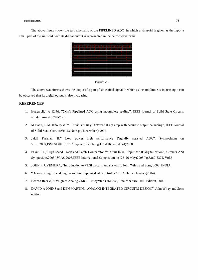
The above figure shows the test schematic of the PIPELINED ADC in which a sinusoid is given as the input a
small part of the sinusoid with its digital output is represented in the below waveforms.
Figure 23
The above waveforms shows the output of a part of sinusoidal signal in which as the amplitude is increasing it can
be observed that its digital output is also increasing.
REFERENCES
1. Iroaga .E,” A 12 bit 75Ms/s Pipelined ADC using incomplete settling”, IEEE journal of Solid State Circuits
vol.42,Issue 4,p.748-756.
2. M Banu, J. M. Khoury & Y. Tsividis “Fully Differential Op-amp with accurate output balancing”, IEEE Journal
of Solid State CircuitsVol.23,No.6 pp, December(1990).
3. Jalali Farahan. B,” Low power high performance Digitally assisted ADC”, Symposiuum on
VLSI,2008,ISVLSI’08,IEEE Computer Society,pg.111-116,(7-9 April)2008
4. Pakau. H ,”High speed Track and Latch Comparator with rail to rail input for IF digitalization”, Circuits And
Symposium,2005,ISCAS 2005,IEEE International Symposium on (23-26 May)2005 Pg.5369-5372, Vol.6
5. JOHN P. UYEMURA, “Introduction to VLSI circuits and systems”, John Wiley and Sons, 2002, INDIA.
6. “Design of high speed, high resolution Pipelined AD controller” P.J.A Harpe. January(2004)
7. Behzad Razavi, “Design of Analog CMOS Integrated Circuits”, Tata McGraw-Hill Edition, 2002.
8. DAVID A JOHNS and KEN MARTIN, “ANALOG INTEGRATED CIRCUITS DESIGN”, John Wiley and Sons
edition.
