plug and play isa specification v1 - osdever.net · the isa bus is the most popular expansion...
TRANSCRIPT

Plug and Play ISASpecification
Version 1.0aMay 5, 1994

Revision History
Issue DateIssue Date CommentsComments
March 1, 1993 Preliminary draft
March 27, 1993 Revised based on review comments
April 29, 1993 Revised based on review comments
May 28, 1993 Release 1.0
March 24, 1994 Release 1.0a. Incorporated eratta and clarifications. OBSOLETED
May 5, 1994 Release 1.0a. Final Changes: -Incorporated clarifications from ‘eratta.doc’ -Additional clarification on order of resource descriptors -Additional clarification on use of dependent functions -Added support for 32-bit memory -Clarified structure of Vendor ID and use of Logical Device ID -Removed redundancies and contradictions with BIOS specification
Microsoft and Intel do not make any representation or warranty regarding this specification or anyproduct or item developed based on this specification. Microsoft and Intel disclaim all express andimplied warranties, including but not limited to the implied warranties of merchantability, fitness for aparticular purpose and freedom from infringement. Without limiting the generality of the foregoing,Microsoft and Intel do not make any warranty of any kind that any item developed based on this
specification, or any portion of it, will not infringe any copyright, patent, trade secret or other intellectualproperty right of any person or entity in any country. It is your responsibility to seek licenses for suchintellectual property rights where appropriate. Microsoft and Intel shall not be liable for any damages
arising out of or in connection with the use of this specification, including liability for lost profit, businessinterruption, or any other damages whatsoever. Some states do not allow the exclusion or limitation of
liability for consequential or incidental damages; the above limitation may not apply to you.
Plug and Play ISA SpecificationPlug and Play ISA Specification(c) Copyright 1993, 1994 by Intel Corporation and Microsoft Corporation.(c) Copyright 1993, 1994 by Intel Corporation and Microsoft Corporation.

P lu g a n d P la y IS A S p e c if ic a t io n i
Table of ContentsRevision HistoryRevision History ................................................................ ................................................................ ................................................................ ................................................................ ................................................................ ................................................................ .......................................... iiii1. Introduction1. Introduction ................................................................ ................................................................ ................................................................ ................................................................ ................................................................ ................................................................ ....................................................22
1.1. Goals.............................................................................................................................................................................................................................................................................................................................31.2. Implementation Considerations........................................................................................................................................................................................................................................3
2. Auto2. Auto-configuration Sequence-configuration Sequence ................................................................ ................................................................ ................................................................ ................................................................ ................................................................ ..................442.1. Plug and Play System Configuration Sequence.............................................................................................................................................................................42.2. Plug and Play Card Configuration Sequence...................................................................................................................................................................................6
3. Isolation and Identification3. Isolation and Identification ................................................................ ................................................................ ................................................................ ................................................................ ................................................................ ..................................773.1. Auto-configuration Ports.........................................................................................................................................................................................................................................................7
3.1.1. ADDRESS Port.......................................................................................................................................................................................................................................................................83.1.2. WRITE_DATA Port....................................................................................................................................................................................................................................................83.1.3. READ_DATA Port........................................................................................................................................................................................................................................................8
3.2. Initiation Key...............................................................................................................................................................................................................................................................................................83.3. Isolation Protocol .................................................................................................................................................................................................................................................................................9
3.3.1. Hardware Protocol ............................................................................................................................................................................................................................................................113.3.2. Software Protocol.......................................................................................................................................................................................................................................................... 12
4. Programming Plug and Play Devices4. Programming Plug and Play Devices ................................................................ ................................................................ ................................................................ ................................................................ .................................. 13134.1. State Summary ......................................................................................................................................................................................................................................................................................134.2. Plug and Play Register Summary.................................................................................................................................................................................................................. 144.3. Control Register Summary..............................................................................................................................................................................................................................................154.4. Plug and Play Isolation Sequence....................................................................................................................................................................................................................... 194.5. Reading Resource Data......................................................................................................................................................................................................................................................204.6. Configuring Card Resource Usage.................................................................................................................................................................................................................20
4.6.1. Order of Configuration Reads .................................................................................................................................................................................................................214.6.2. Resource Programming.....................................................................................................................................................................................................................................22
4.7. Run Time Access to Plug and Play registers..............................................................................................................................................................................235. Plug and Play Functionality5. Plug and Play Functionality ................................................................ ................................................................ ................................................................ ................................................................ ................................................................ .................. 2424
5.1. Minimum Functionality for a Configurable Logical Device .................................................................................................................................245.2. Minimum Level of Functionality for a Non-configurable Logical Device .............................................................................24
6. Plug and Play Resources6. Plug and Play Resources ................................................................ ................................................................ ................................................................ ................................................................ ................................................................ ..................................25256.1. Serial Identifier .....................................................................................................................................................................................................................................................................................25
6.1.1. Vendor ID....................................................................................................................................................................................................................................................................................266.1.2. Serial/Unique Number ...........................................................................................................................................................................................................................................266.1.3. Checksum.....................................................................................................................................................................................................................................................................................26
6.2. Plug and Play Resource Data Types ........................................................................................................................................................................................................276.2.1. Resource Data Requirements....................................................................................................................................................................................................................276.2.2. Small Resource Data Type.........................................................................................................................................................................................................................28
6.2.2.1. Plug and Play Version Number.........................................................................................................................................................................................296.2.2.2. Logical Device ID....................................................................................................................................................................................................................................306.2.2.3. Compatible Device ID..........................................................................................................................................................................................................................316.2.2.4. IRQ Format .........................................................................................................................................................................................................................................................326.2.2.5. DMA Format....................................................................................................................................................................................................................................................336.2.2.6. Start Dependent Functions ......................................................................................................................................................................................................... 346.2.2.7. End Dependent Functions............................................................................................................................................................................................................ 346.2.2.8. I/O Port Descriptor..................................................................................................................................................................................................................................356.2.2.9. Fixed Location I/O Port Descriptor ......................................................................................................................................................................... 366.2.2.10. Vendor Defined.......................................................................................................................................................................................................................................... 366.2.2.11. End Tag.................................................................................................................................................................................................................................................................... 36
ii P lu g a n d P la y IS A S p e c if ic a t io n
6.2.3. Large Resource Data Type.......................................................................................................................................................................................................................376.2.3.1. Memory Range Descriptor...........................................................................................................................................................................................................386.2.3.2. ANSI Identifier String .........................................................................................................................................................................................................................406.2.3.3. Unicode Identifier String..................................................................................................................................................................................................................406.2.3.4. Vendor Defined ..............................................................................................................................................................................................................................................416.2.3.5. 32-bit Memory Range Descriptor..................................................................................................................................................................................416.2.3.6. 32-bit Fixed Location Memory Range Descriptor.........................................................................................................................44
7. Resource Data and Dependent Functions7. Resource Data and Dependent Functions ................................................................ ................................................................ ................................................................ ................................................................ .................. 46467.1. Example One.........................................................................................................................................................................................................................................................................................467.2. Example Two.....................................................................................................................................................................................................................................................................................477.3. Example Three.................................................................................................................................................................................................................................................................................477.4. Example Four ....................................................................................................................................................................................................................................................................................47
Appendix A. Plug and Play Standard RegistersAppendix A. Plug and Play Standard Registers ................................................................ ................................................................ ................................................................ ........................................................ 4949A.1. Plug and Play Card Control Registers.....................................................................................................................................................................................................50A.2 Plug and Play Logical Device Control Registers.................................................................................................................................................................52A.3. Plug and Play Logical Device Configuration Registers.............................................................................................................................................53
A.3.1. Memory Configuration Registers.......................................................................................................................................................................................................53A.3.2. I/O Configuration Registers......................................................................................................................................................................................................................57A.3.3. Interrupt Configuration Registers.......................................................................................................................................................................................................58A.3.4. DMA Configuration Registers.............................................................................................................................................................................................................59A.3.5. Reserved and Vendor Defined Configuration Registers.........................................................................................................................59
A.4. Reserved Register.......................................................................................................................................................................................................................................................................59Appendix B. LFSR DefinitionAppendix B. LFSR Definition ................................................................ ................................................................ ................................................................ ................................................................ ................................................................ ......................6060
B.1. Initiation LFSR Function.....................................................................................................................................................................................................................................................60B.2. LFSR Checksum Functions..........................................................................................................................................................................................................................................61
Appendix C. Possible EnhancementsAppendix C. Possible Enhancements ................................................................ ................................................................ ................................................................ ................................................................ .................................................. 6262C.1. Plug and Play Boot Devices......................................................................................................................................................................................................................................62C.2. BIOS Support for Plug and Play Devices......................................................................................................................................................................................63C.3. Plug and Play Devices and Non-Plug and Play Operating Systems...............................................................................................63
Appendix D. Sample Configuration Record for ABC Ethernet CardAppendix D. Sample Configuration Record for ABC Ethernet Card ................................................................ ................................................................ ...... 6464
List of TablesTable 1. Auto-configuration Ports ...................................................................................................................................................................................................................................................7Table 2. Plug and Play Header.....................................................................................................................................................................................................................................................25Table 3. Small Resource Data Type Tag Bit Definitions.................................................................................................................................................................28Table 4. Small Resource Items ........................................................................................................................................................................................................................................................28Table 5. Large Resource Data Type Tag Bit Definitions...............................................................................................................................................................37Table 6. Large Resource Items ......................................................................................................................................................................................................................................................37Table A-1. Plug and Play Standard Registers.......................................................................................................................................................................................................50Table A-2. Plug and Play Logical Device Control Registers...................................................................................................................................................52Table A-3. Memory Space Configuration..................................................................................................................................................................................................................54Table A-4. 32-bit Memory Space Configuration...........................................................................................................................................................................................55Table A-5. I/O Space Configuration....................................................................................................................................................................................................................................57Table A-6. Interrupt Configuration ...........................................................................................................................................................................................................................................58Table A-7. DMA Channel Configuration ....................................................................................................................................................................................................................59Table A-8. Logical Device Configuration....................................................................................................................................................................................................................59Table A-9. Logical Device Reserved.................................................................................................................................................................................................................................59
P lu g a n d P la y IS A S p e c if ic a t io n iii
List of FiguresFigure 1. ISA Configuration Flow for Existing Non-Plug and Play BIOS............................................................................................................4Figure 2. Plug and Play ISA Configuration Flow for Plug and Play BIOS......................................................................................................5Figure 3. Logic Flow for Auto-configuration...........................................................................................................................................................................................................7Figure 4. Plug and Play ISA Card Isolation Algorithm...........................................................................................................................................................................9Figure 5. Shifting of Serial Identifier.......................................................................................................................................................................................................................................10Figure 6. Plug and Play High-Level Register Map.................................................................................................................................................................................... 14Figure 7. Serial Identifier and Resource Data......................................................................................................................................................................................................... 16Figure 8. Plug and Play ISA Card State Transitions...................................................................................................................................................................................18Figure A-1. Plug and Play Register Map.....................................................................................................................................................................................................................49Figure B-1. Initiation Key LFSR...................................................................................................................................................................................................................................................60Figure B-2. Checksum LFSR.............................................................................................................................................................................................................................................................61


P lu g a n d P la y IS A S p e c if ic a t io n 1
Abstract
This specification presents a mechanism to provide automatic configuration capability to In d u s t r y S t a n d a r dA r c h i te c t u r e (ISA) cards thus enabling full Plug and Play in the PC. The essential elements of Plug and PlayISA are:
• Isolate the ISA card
• Read the card's resource data
• Identify the card and configure its resources
• Locate a driver for the card
The mechanism has the flexibility to allow cards to come up either inactive or active. Cards required toparticipate in the boot process typically come up active. Information that identifies the card and describes thesystem resources which are requested by the card, such as memory and I/O space, DMA channel, andinterrupt level supported is maintained in a standard read-only format. This allows the Plug and Playsoftware to identify system resource usage, arbitrate conflicts, and, optionally, re-configure a card. Thisprocess is done automatically at every hard reset of the system. Plug and Play ISA cards will inter-operatewith standard ISA cards in a fully compatible manner.
Possible BIOS extensions required to support Plug and Play ISA cards are also discussed in this specification.However, user interface issues for installation of device drivers are not addressed.
2 P lu g a n d P la y IS A S p e c if ic a t io n
1. Introduction
The ISA bus is the most popular expansion standard in the PC industry. The bus architecture requires theallocation of memory and I/O address spaces, DMA channels and interrupt levels among multiple ISA cards.However, the ISA interface has no defined hardware or software mechanism for allocating these resources.As a result, configuration of ISA cards is typically done with “jumpers” that change the decode maps formemory and I/O space and steer the DMA and interrupt signals to different pins on the bus. Further,system configuration files may need to be updated to reflect these changes. Users typically resolve sharingconflicts by referring to documentation provided by each card manufacturer. For the average user, thisconfiguration process can be unreliable and frustrating.
Alternative bus standards (for example, Micro Channel and EISA) have hardware and software mechanismsto identify the resources requested by a card and resolve conflicts. These mechanisms are not compatiblewith the installed base of PCs with ISA card slots.
This specification proposes a hardware and software mechanism for incorporation in the next generation ofISA cards, referred to as Plug and Play ISA cards, that enables resolution of conflicts between Plug and PlayISA cards. In other words, the Plug and Play software optimally allocates system resources between the Plugand Play ISA cards and other devices in the system without user intervention.
In a system that uses only Plug and Play ISA cards, it will be possible to achieve full auto- configuration.However, it is recognized that the current generation or standard ISA cards will co-exist with Plug and PlayISA cards in the same system. In such systems, the configuration solution needs to be augmented in theBIOS and/or operating system to manage and arbitrate ISA bus resources. User interaction may still benecessary in some cases.
This specification defines mechanisms that each Plug and Play ISA card must implement to supportidentification, resource usage determination, conflict detection, and conflict resolution. This specification alsopresents a process for Plug and Play software to automatically configure the new cards without userintervention.

P lu g a n d P la y IS A S p e c if ic a t io n 3
1.1. Goals
The following are the architectural goals to support full Plug-and-Play of ISA systems:
1. Focus on ease-of-use for the end-user
2. Provide the ability to uniquely address individual cards even when two or more cards are configuredto use the same system resources.
3. Define a protocol that provides the ability to read a configuration template on each card whichidentifies current resource usage and options for each system resource requested on each card
4. Define a mechanism to set or modify the current configuration of each card
5. Provide a range of cost-benefit compliance points
6. Maintain backward and forward compatibility as follows:
• Plug and Play ISA cards will electrically and functionally inter-operate with standard ISA cards inany existing ISA based PC system; however, the system may not be fully auto-configurable.
• With the addition of Plug and Play software (i.e. utilities, BIOS enhancements or operatingsystem enhancements, and user interrogation), the above system can be made increasingly auto-configurable.
• A system with only Plug and Play ISA cards and appropriate software will be fully auto-configurable.
1.2. Implementation Considerations
The solution of the ISA configuration problem addresses major concerns of end-users, system integrators, ISAcard manufacturers, and operating system vendors. It also presents an excellent business opportunity forproviding measurable value and differentiation in the short term.
In defining this mechanism, the cost of incremental hardware has been taken into consideration. Thespecification allows an implementor to make tradeoffs in the area of technology and level of integrationdepending on the functionality and market for each card.
4 P lu g a n d P la y IS A S p e c if ic a t io n
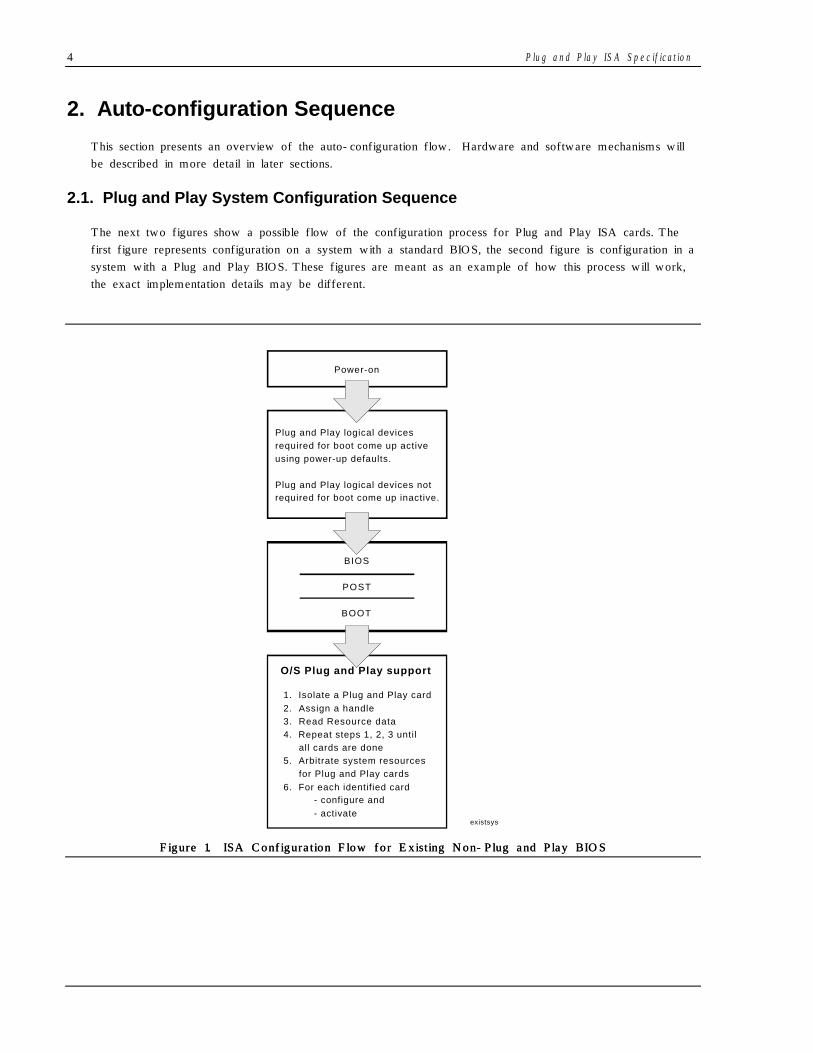
2. Auto-configuration Sequence
This section presents an overview of the auto-configuration flow. Hardware and software mechanisms willbe described in more detail in later sections.
2.1. Plug and Play System Configuration Sequence
The next two figures show a possible flow of the configuration process for Plug and Play ISA cards. Thefirst figure represents configuration on a system with a standard BIOS, the second figure is configuration in asystem with a Plug and Play BIOS. These figures are meant as an example of how this process will work,the exact implementation details may be different.
existsys
Power-on
Plug and Play logical devicesrequired for boot come up activeusing power-up defaults.
Plug and Play logical devices notrequired for boot come up inactive.
BIOS
POST
BOOT
1. Isolate a Plug and Play card
2. Assign a handle3. Read Resource data4. Repeat steps 1, 2, 3 until all cards are done5. Arbitrate system resources for Plug and Play cards
6. For each identified card - configure and
- activate
O/S Plug and Play support
Figure Figure 11 . ISA Configuration Flow for Existing Non. ISA Configuration Flow for Existing Non-Plug and Play BIOS-Plug and Play BIOS

P lu g a n d P la y IS A S p e c if ic a t io n 5
Power-on
Plug and Play logical devicesrequired for boot come up activeusing power-up defaults.
Plug and Play logical devices notrequired for boot come up inactive.
1. Get Plug and Play information
from BIOS2. Read resource data from all cards3. Arbitrate system resources for Plug and Play cards4. Assign conflict-free resources
for all inactive logical devices5. Activate all logical devices just configured7. Load device drivers
O/S Plug and Play support
Before POST, BIOS will,
1. Isolate a Plug and Play card2. Assign a handle3. Read Resource data4. Repeat steps 1, 2, 3 until all cards are done
5. For each logical device required for boot, a. Check if resource assignments are conflict free
b. Activate the logical device6. Optionally, configure all other logical devices and configure or leave them in inactive state
POST
BOOT
upgrdsys
Figure Figure 22. Plug and Play ISA Configuration Flow for Plug and Play BIOS. Plug and Play ISA Configuration Flow for Plug and Play BIOS
6 P lu g a n d P la y IS A S p e c if ic a t io n
2.2. Plug and Play Card Configuration Sequence
The major steps of the auto-configuration process are as follows:
• Put all Plug and Play ISA cards in configuration mode
• Isolate one Plug and Play ISA card at a time
• Assign a handle and read the card's resource data structure
• After the resource requirements and capabilities are determined for all cards, use the handle to assignconflict free resources to each card
• Activate all Plug and Play ISA cards and remove them from configuration mode
The Plug and Play software identifies and configures devices using a set of commands defined in thisspecification. The commands are executed using three, 8-bit I/O ports. 16-bit accesses (assertion ofIOCS16#) to the configuration ports are not supported. A sequence of data writes to one of the ports isused as the key to enable the Plug and Play logic on all cards in the system. This sequence, referred to asthe initiation key, is described in the next section.
All Plug and Play cards respond to the same I/O port addresses so the Plug and Play software needs anisolation mechanism to address one particular card at a time. The isolation protocol uses a unique number oneach card to isolate one Plug and Play card at a time. After isolation, the Plug and Play software assignseach card a handle, which is used to select that unique Plug and Play card. The use of the handle eliminatesthe need to use the more elaborate and time consuming isolation protocol to select a unique card.
Each card supports a readable resource data structure that describes the resources supported and thoserequested by the functions on that card. The structure supports the concept of multiple functions per ISAcard. Each function is defined as a logical device. Plug and Play resource information is provided for eachlogical device and each logical device is independently configured through the Plug and Play standard registers.
Following isolation, the Plug and Play software reads the resource data structure on each card. When allresource capabilities and demands are known, a process of resource arbitration is invoked to determineresource allocation to each ISA card.
The configuration of ISA cards is done using the command registers specified for each resource type. Itshould be noted that some ISA functions may not be re-configurable. In these cases, the resources requestedwill be equivalent to the resources supported. However, the resource data structure informs the arbiter that itcannot assign these resources to other Plug and Play cards in the system.
After the assignment of resources, an I/O conflict detection mechanism may be invoked. This mechanismprovides a means to insure that I/O resources assigned are not in conflict with standard ISA cards.
The command set also supports the ability to activate or deactivate the function(s) on the card.
After configuration is complete, Plug and Play cards are removed from configuration mode. To re-enableconfiguration mode, the initiation key needs to be re-issued. This prevents accidental erasure of theconfiguration information.
P lu g a n d P la y IS A S p e c if ic a t io n 7
3. Isolation and Identification
This section specifies the assignment of auto-configuration ports and the isolation protocol.
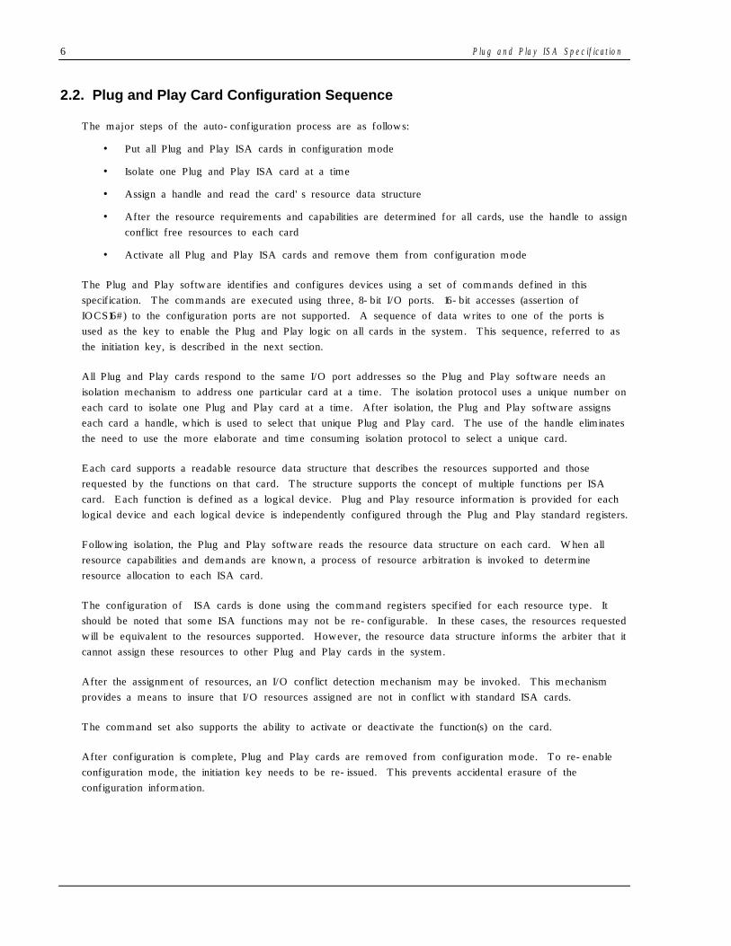
3.1. Auto-configuration Ports
Three 8-bit ports are used by the software to access the configuration space on each Plug and Play ISAcard. The ports are listed in table 1. The configuration space is implemented as a set of 8-bit registers.These registers are used by the Plug and Play software to issue commands, check status, access the resourcedata information, and configure the Plug and Play hardware.
The ports have been chosen so as to avoid conflicts in the installed base of ISA functions, while at the sametime minimizing the number of ports needed in the ISA I/O space.
Table Table 11 . Auto-configuration Ports. Auto-configuration Ports
Port NamePort Name LocationLocation TypeType
ADDRESS 0x0279 (Printer status port) Write-only
WRITE_DATA 0x0A79 (Printer status port + 0x0800) Write-only
READ_DATA Relocatable in range 0x0203 to 0x03FF Read-only
The ADDRESS and WRITE_DATA ports are located at fixed addresses. The WRITE_DATA port islocated at an address alias of the ADDRESS port. All three auto-configuration ports use a 12-bit ISA addressdecode.
The READ_DATA port is relocatable within the I/O range from 0x0203h to 0x03FFh. This is the onlyreadable auto-configuration port.
pnp_arch
Logical deviceconfiguration
Logical devicecontrol
Cardcontrol
Addressregister
LFSRkey
ISA Bus
DecoderADDRESS port
WRITE_DATA port
READ_DATA port
ENABLE
SELECT
OUTPUT
ENABLE
ADDR[11:00]
CONTROL
DATA[7:0]
Figure Figure 33. Logic Flow for Auto-configuration. Logic Flow for Auto-configuration

8 P lu g a n d P la y IS A S p e c if ic a t io n
3.1.1. ADDRESS Port
The Plug and Play registers are accessed by first writing the address of the desired register to theADDRESS port, followed by a read of data from the READ_DATA port or a write of data to theWRITE_DATA port. A write to the ADDRESS port may be followed by any number of WRITE_DATAor READ_DATA accesses to the same register location without the need to write to the ADDRESS portbefore each access.
The ADDRESS port is also the write destination of the initiation key, which is described later.
3.1.2. WRITE_DATA Port
The WRITE_DATA port is used to write information to the Plug and Play registers. The destination of thedata is determined by the last setting of the ADDRESS port.
3.1.3. READ_DATA Port
The READ_DATA port is used to read information from the Plug and Play registers. The source of thedata is determined by the last setting of the ADDRESS port.
The address of the READ_DATA port is set by writing the proper value to a Plug and Play control register.The isolation protocol verifies that the location selected for the READ_DATA port is free of conflict.
3.2. Initiation Key
The Plug and Play logic is quiescent on power up and must be enabled by software.
The initiation key places the Plug and Play logic into configuration mode. This is done by a predefined seriesof writes to the ADDRESS port. The write sequence is decoded by on-card logic. If the proper series ofI/O writes is detected, then the Plug and Play auto-configuration ports are enabled.
The hardware check of the initiation key is implemented as a lin e a r f e e d b a c k s h if t r e g is t e r (LFSR). Ahardware diagram of the LFSR is shown in the Appendix B.
Software generates the LFSR sequence and writes it to the ADDRESS port as a sequence of 8-bit writecycles. The hardware compares the byte of write data with the value in the shift register at each write.Any time the data does not match, the hardware will reset to the initial value of the LFSR. Software shouldreset the LFSR to its initial value by a sequence of two write cycles of 0x00 to the ADDRESS port beforethe initiation key is sent.
The initial value of the LFSR and the exact sequence are documented in Appendix B.

P lu g a n d P la y IS A S p e c if ic a t io n 9
3.3. Isolation Protocol
A simple algorithm is used to isolate each Plug and Play card. This algorithm uses the signals on the ISAbus and requires lock-step operation between the Plug and Play hardware and the isolation software.
isolalgr
no
Wait for next read from serial isolation register
SDL[1:0] = "01"
ID bit = "1H"
SDL[1:0] = "10"
StateSleep
Get one bit from serial identifierRead from serial isolation register
no
noyes
yes
yes
Drive "55H"on SDL[7:0] Leave SDL
in high-impedance
Drive "AAH"on SDL[7:0]
Leave SDLin high impedance
After I/O read completes,fetch next ID bit from
serial identifierID=0;
other card ID=1
StateIsolation
yes
no
One cardisolated
Read all 72 bitsfrom serial
identifer
Figure Figure 44. Plug and Play ISA Card Isolation Algorithm. Plug and Play ISA Card Isolation Algorithm
10 P lu g a n d P la y IS A S p e c if ic a t io n
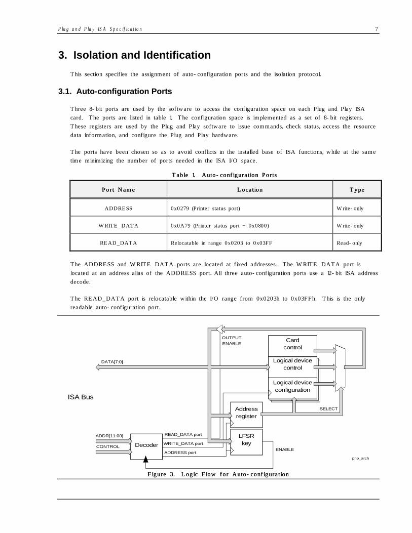
3.3. Isolation Protocol (cont.)
The key element of this mechanism is that each card contains a unique number, referred to as the s e r ia lid e n t if ie r for the rest of the discussion. The serial identifier is a 72-bit unique, non-zero, number composedof two, 32-bit fields and an 8-bit checksum. The first 32-bit field is a vendor identifier. The other 32 bitscan be any value, for example, a serial number, part of a LAN address, or a static number, as long as therewill never be two cards in a single system with the same 64 bit number. The serial identifier is accessedbit-serially by the isolation logic and is used to differentiate the cards. Refer to section 6.1. S e r ia l I d e n t if ie r ,for further information.
serialid
Byte 0
Vendor ID
7:0
Byte 1
7:0
Byte 2
7:0
Byte 3
7:0
Byte 0
7:0
Byte 1
7:0
Byte 2
7:0
Byte 3
7:0
Byte 0
7:0
Serial NumberCheck-
sum
Shift
Figure Figure 55. . Shifting of Serial IdentifierShifting of Serial Identifier
The shift order for all Plug and Play serial isolation and resource data is defined as bit[0], bit[1], and so onthrough bit[7].

P lu g a n d P la y IS A S p e c if ic a t io n 11
3.3.1. Hardware Protocol
The isolation protocol can be invoked by the Plug and Play software at any time. The initiation key,described earlier, puts all cards into configuration mode. The hardware on each card expects 72 pairs of I/Oread accesses to the READ_DATA port. The card's response to these reads depends on the value of eachbit of the serial identifier which is being examined one bit at a time, in the sequence shown in figure 5.
If the current bit of the serial identifier is a “1”, then the card will drive the data bus to 0x55 to completethe first I/O read cycle. If the bit is “0”, then the card puts its data bus driver into high impedance. Allcards in high impedance will check the data bus during the I/O read cycle to sense if another card is drivingD[1:0] to “01.” During the second I/O read, the card(s) that drove the 0x55, will now drive a 0xAA. Allhigh impedance cards will check the data bus to sense if another card is driving D[1:0] to “10.”
If a high impedance card sensed another card driving the data bus with the appropriate data during bothcycles, then that card ceases to participate in the current iteration of card isolation. Such cards, which loseout, will participate in future iterations of the isolation protocol.
NOTE:NOTE: D u r in g e a c h r e a d c y c le , th e P lu g a n d P la y h a r d w a r e d r iv e s t h e e n t i re 8 - b i t d a t ab u s , b u t o n ly c h e c k s t h e lo w e r 2 b i t s .
If a card was driving the bus or if the card was in high impedance and did not sense another card drivingthe bus, then it should prepare for the next pair of I/O reads. The card shifts the serial identifier by one bitand uses the shifted bit to decide its response.
The above sequence is repeated for the entire 72-bit serial identifier.
At the end of this process, one card remains. This card is assigned a handle referred to as the C a r d S e le c tN u m b e r (CSN) that will be used later to select the card. Cards which have been assigned a CSN will notparticipate in subsequent iterations of the isolation protocol. Cards must be assigned a CSN before they willrespond to the other commands defined in the specification.
It should be noted that the protocol permits the 8-bit checksum to be stored in non-volatile memory on thecard or generated by the on-card logic in real-time. The same LFSR algorithm described in the initiationkey section is used in the checksum generation. The exact description of the checksum algorithm and anexample are shown in Appendix B.
Plug and Play cards must not drive the IOCHRDY signal during serial isolation. However, cards may driveIOCHRDY at any other time.

12 P lu g a n d P la y IS A S p e c if ic a t io n
3.3.2. Software Protocol
The Plug and Play software sends the initiation key to all Plug and Play cards to place them intoconfiguration mode. The software is then ready to perform the isolation protocol.
The Plug and Play software generates 72 pairs of I/O read cycles from the READ_DATA port. Thesoftware checks the data returned from each pair of I/O reads for the 0x55 and 0xAA driven by thehardware. If both 0x55 and 0xAA are read back, then the software assumes that the hardware had a “1”bit in that position. All other results are assumed to be a “0.”
During the first 64 bits, software generates a checksum using the received data. The checksum is comparedwith the checksum read back in the last 8 bits of the sequence.
There are two other special considerations for the software protocol. During an iteration, it is possible thatthe 0x55 and 0xAA combination is never detected. It is also possible that the checksum does not match. Ifeither of these cases occur on the first iteration, it must be assumed that the READ_DATA port is inconflict. If a conflict is detected, then the READ_DATA port is relocated. The above process is repeateduntil a non-conflicting location for the READ_DATA port is found. The entire range between 0x200 and0x3FF is available, however in practice it is expected that only a few locations will be tried before softwaredetermines that no Plug and Play cards are present.
During subsequent iterations, the occurrence of either of these two special cases should be interpreted as theabsence of any further Plug and Play cards (i.e. the last card was found in the previous iteration). Thisterminates the isolation protocol.
NOTE:NOTE: T h e s o f t w a r e m u s t d e la y 1 m s e c p r io r t o s t a r t in g t h e f i r s t p a i r o f i s o l a t i o n r e a d s ,a n d m u s t w a i t 2 5 0 µs e c b e t w e e n e a c h s u b s e q u e n t p a ir o f is o la t io n r e a d s . T h isd e la y g iv e s t h e IS A c a r d t im e t o a c c e s s in f o r m a t io n f r o m p o s s ib ly v e r y s lo ws t o r a g e d e v ic e s .
P lu g a n d P la y IS A S p e c if ic a t io n 13
4. Programming Plug and Play Devices
This section describes how configuration resource data is read from Plug and Play ISA cards as well as howresource selections are programmed. The Plug and Play state machine and Plug and Play commands areintroduced. The Plug and Play state machine is shown in figure Error! Bookmark not defined.Error! Bookmark not defined. . Addressesfor Plug and Play registers are summarized in Appendix A.
4.1. State Summary
Before explaining the Plug and Play state transitions it is necessary to introduce a register in each ISA cardcalled the C a r d S e le c t N u m b e r (CSN). The CSN is an 8-bit register used to select one or more ISA cardswhen those cards are in certain states. The CSN is defined as an 8-bit register to allow a wide variety ofdevices to manage their configuration and control using this mechanism. The CSN is defined such that allcards power-up with this register is set to 0x0. Once a card has been isolated, the CSN on that card isassigned a unique value. This value enables the Plug and Play software to select this card at later points inthe configuration process, without going through the isolation protocol again.
The Plug and Play states are summarized as follows:
• W a i t f o r K e y W a i t f o r K e y - All cards enter this state after power-up reset or in response to the Reset and Waitfor Key commands. No commands are active in this state until the initiation key is detected on the ISAbus. The W a i t f o r K e yW a i t f o r K e y state is the default state for Plug and Play cards during normal systemoperation. After configuration and activation, software should return all cards to this state.
• S l e e pS l e e p - In this state, Plug and Play cards wait for a Wake[CSN] command. This command willselectively enable one or more cards to enter either the I s o l a t i o nI s o l a t i o n or C o n f i gC o n f i g states based on the writedata and the value of the CSN on each card. Cards leave the S l e e pS l e e p state in response to a Wake[CSN]command when the value of write data bits[7:0] of the Wake[CSN] command matches the card’s CSN.If the write data for the Wake[CSN] command is zero then all cards that have not been assigned aCSN will enter the I s o l a t i o nI s o l a t i o n state. If the write data for the Wake[CSN] command is not zero then theone card whose assigned CSN matches the parameter of the Wake[CSN] command will enter theC o n f i gC o n f i g state.
• I s o l a t i o nI s o l a t i o n - In this state, Plug and Play cards respond to reads of the Serial Isolation register as describedin the previous chapter on isolation protocol. Once a card is isolated, a unique CSN is assigned. Thisnumber will later be used by the Wake[CSN] command to select the card. Once the CSN is written,the card transitions to the C o n f i gC o n f i g state.
• C o n f i gC o n f i g - A card in the C o n f i gC o n f i g state responds to all configuration commands including reading thecard's resource configuration information and programming the card's resource selections. Only onecard may be in this state at a time.
14 P lu g a n d P la y IS A S p e c if ic a t io n
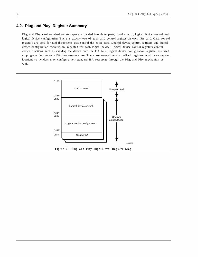
4.2. Plug and Play Register Summary
Plug and Play card standard register space is divided into three parts; card control, logical device control, andlogical device configuration. There is exactly one of each card control register on each ISA card. Card controlregisters are used for global functions that control the entire card. Logical device control registers and logicaldevice configuration registers are repeated for each logical device. Logical device control registers controldevice functions, such as enabling the device onto the ISA bus. Logical device configuration registers are usedto program the device's ISA bus resource use. There are several vendor defined registers in all three registerlocations so vendors may configure non-standard ISA resources through the Plug and Play mechanism aswell.
confgmp2
Card control
0x00
0x2F
One perlogical device
One per card
Logical device control
Logical device configuration
Reserved
0x30
0x3F0x40
0xFE
0xFF
Figure Figure 66. Plug and Play High-Level Register Map. Plug and Play High-Level Register Map

P lu g a n d P la y IS A S p e c if ic a t io n 15
4.3. Control Register Summary
Plug and Play cards respond to commands written to Plug and Play registers as well as certain ISA busconditions. These commands are summarized below:
• RESET_DRV - This is the ISA bus reset signal. When a Plug and Play card detects this signal it entersthe W a i t f o r K e y W a i t f o r K e y state. All CSNs are reset to 0x0. The configuration registers for all logical devicesare loaded with their power-up values from non-volatile memory or jumpers. All non-boot logicaldevices become inactive. Boot devices become active using their power-up ISA resources.
Note: The software must delay 1 msec after RESET_DRV before accessing the auto-configurationports.
• Config control register - The Config Control register consists of three independent commands which areactivated by writing a “1” to their corresponding register bits. These bits are automatically reset to “0”by the hardware after the commands execute.
• Reset command - The Reset command is sent to the Plug and Play cards by writing a value of0x01 to the Config Control register. All Plug and Play cards in any state, except Wait for KeyWait for Key,respond to this command. This command performs a reset function on all logical devices. Thisresets the contents of configuration registers to their default state. The configuration registers for alllogical devices are loaded with their power-up values from non-volatile memory or jumpers. TheREAD_DATA port, CSN and Plug and Play state are preserved.
Note: The software must delay 1 msec after issueing the reset command before accessing theauto-configuration ports.
• Wait for Key command - The Wait for Key command is sent to the Plug and Play cards bywriting a value of 0x02 to the Config Control register. All Plug and Play cards in any state willrespond to this command. This command forces all Plug and Play cards to enter the W a i t f o rW a i t f o rK e yK e y state. The CSNs are preserved and no logical device status is changed.
• Reset CSN command - The Reset CSN command is sent to the Plug and Play cards by writing avalue of 0x04 to the Config Control register. All Plug and Play cards in any state, except Wait forWait forKeyKey, will reset their CSN to 0.
Im p le m e n t o r ' s n o t e : O n a C T R L - A L T - D E L k e y s e q u e n c e , th e B IO S is s u e s a r e s e t o f a ll lo g ic a ld e v ic e s , re s t o r e s c o n f ig u r a t io n r e g is t e r s t o t h e i r d e f a u l t v a lu e s , a n d r e t u r n s a ll c a r d s t o t h e W a i t f o rW a i t f o rK e y K e y s t a t e ( i .e ., w r i t e a v a lu e o f 0 x 0 3 t o t h e C o n f ig C o n t r o l re g is t e r ) . T h is r e t a in s t h e C S N s a n dR E A D _ D A T A p o r t a n d w ill e lim in a t e t h e n e e d t o g o t h r o u g h t h e is o la t io n s e q u e n c e a g a in . A w r i t et o t h is r e g is t e r w i th a ll th r e e b i t s s e t is e q u iv a le n t t o a R E S E T _ D R V e v e n t .
• Set RD_DATA Port command - This command sets the address of the READ_DATA Port for all Plugand Play cards. Write data bits[7:0] is used as ISA I/O bus address bits[09:02]. The ISA bus addressbits[1:0] is fixed at binary “11.” The ISA bus address bits[15:10] is fixed at binary “000000.” Thiscommand can only be used in the I s o l a t i o nI s o l a t i o n state. The exact method for setting the read data port is:
Issue the Initiation KeySend command Wake[0]Send command Set RD_DATA Port
Note: After a RESET_DRV or Reset CSN command, this register is considered uninitialized and mustbe reinitialized.
16 P lu g a n d P la y IS A S p e c if ic a t io n
• Serial Isolation register - A read from the Serial Isolation register causes Plug and Play cards in theI s o l a t i o nI s o l a t i o n state to respond to the ISA bus read cycle as described in the Isolation Protocol section above.Cards that “lose” the isolation protocol will enter the S l e e pS l e e p state.
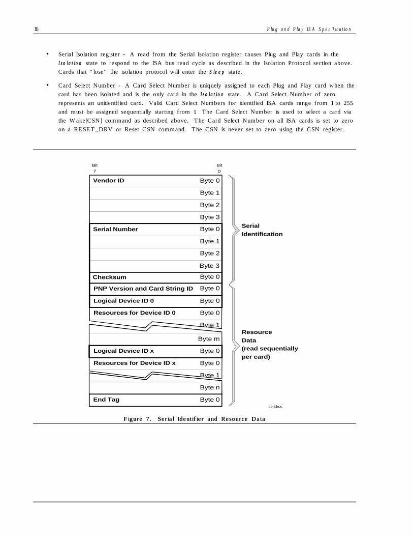
• Card Select Number - A Card Select Number is uniquely assigned to each Plug and Play card when thecard has been isolated and is the only card in the I s o l a t i o nI s o l a t i o n state. A Card Select Number of zerorepresents an unidentified card. Valid Card Select Numbers for identified ISA cards range from 1 to 255and must be assigned sequentially starting from 1. The Card Select Number is used to select a card viathe Wake[CSN] command as described above. The Card Select Number on all ISA cards is set to zeroon a RESET_DRV or Reset CSN command. The CSN is never set to zero using the CSN register.
Byte 0PNP Version and Card String ID
Byte 0
End Tag
Byte 0
Byte 0Serial Number
Byte 3
Byte 2
Byte 1
Byte 0Vendor ID
Byte 1
Byte 2
Byte 3
Bit
7
Bit
0
Serial
Identification
Resource
Data(read sequentially
per card)
seridres
Checksum Byte 0
Logical Device ID 0
Resources for Device ID 0
Byte 1
Byte m
Byte 0
Byte 0Logical Device ID x
Resources for Device ID x
Byte 1
Byte n
Byte 0
Figure Figure 77. Serial Identifier and Resource Data. Serial Identifier and Resource Data
P lu g a n d P la y IS A S p e c if ic a t io n 17
• Wake[CSN] command - This command is used to bring ISA cards in the S l e e pS l e e p state to either theI s o l a t i o nI s o l a t i o n state or the C o n f i gC o n f i g state. A Wake[CSN] command with a parameter of zero will force allcards without a CSN to enter the IsolationIsolation state. A Wake[CSN] command with a parameter other thanzero will force a card with a matching CSN to enter the C o n f i gC o n f i g state. Any card in the I s o l a t i o nI s o l a t i o n orC o n f i gC o n f i g states that receives a Wake[CSN] command with a parameter that does not match its CSN willtransition to the S l e e pS l e e p state.
All Plug and Play cards function as if their 72-bit serial identifier and their resource data come from asingle serial device. The pointer to this data is reset to the beginning whenever a card receives anyWake[CSN] command.
• Resource Data register - A read of the Resource Data register will return one byte of resource datafrom a Plug and Play card in the C o n f i gC o n f i g state. Resource data is always returned byte sequentially.The Status register must always be read to confirm that resource data is available before the ResourceData register is read.
• Status register - Bit[0] of the Status register indicates that the next byte of resource data is available tobe read. If this bit is equal to one then data is available, otherwise resource data is not yet available.The Plug and Play software will poll this location until bit[0] is set, then the next data byte from theResource Data register is read.
• Logical Device Number register - The logical device number register is used to select which logicaldevice the following configuration commands will operate on. Cards may contain more than one logicaldevice, in which case the logical device is selected by writing the 8-bit logical device number into thisregister. The logical device number is determined by the order in which the logical devices are readfrom the resource data. The first logical device number is 0, the second is 1, and so on.
• I/O Range Check register - I/O Range Check register allows the Plug and Play software to determine ifanother card conflicts with the I/O port range that has been assigned to a logical device. The I/O rangecheck works by having all I/O ranges that would be used by a logical device return 0x55 then 0xAA onI/O read commands. The Plug and Play software performs reads to all the ports that would be used bythe logical device and verifies that the correct data is returned. If a conflict is detected, then the Plugand Play software relocates the I/O range of the logical device to a new location. Setting bit[1] of thisregister enables the I/O check range check logic. Setting bit[0] forces the logical device to respond toI/O reads within its assigned I/O range with the value 0x55. If bit[0] is cleared, then the logical deviceresponds to reads within its assigned I/O range with the value of 0xAA. This function operates onlywhen bit[0] of the Activate register (described below) is not set. This command is optional and is notimplemented on cards that do not have configurable I/O port ranges.
• Activate register - The Activate register is a read/write register that is used to activate a logical device.An active logical device responds to all ISA bus cycles as per its normal operation. An inactive logicaldevice does not respond to nor drive any ISA bus signals. Bit[0] is the active bit, if it is set to “1” thenthe logical device is active, otherwise it is inactive.

18 P lu g a n d P la y IS A S p e c if ic a t io n
4.3. Control Register Summary (cont.)
The state transitions for the Plug and Play ISA card are shown below.
statetrn
State Active Commands
Set CSN = 0
Wait for Key no active commands
State Active Commands
Sleep
Reset
Wait for Key
Wake[CSN]
Initiation Key
State Active Commands
Isolation
Reset
Wait for Key
Set RD_DATA PortSerial Isolation
Wake[CSN]
State Active Commands
Config
ResetWait for KeyWake[CSN]Resource DataStatusLogical DeviceI/O Range CheckActivateConfiguration registers
Set CSN
(WAKE <> 0) AND (WAKE = CSN)
WAKE <> CSNLose serial isolation OR(WAKE <> CSN)
(WAKE = 0) AND (CSN = 0)
Power upRESET_DRV orReset command
Notes:1. CSN = Card Select Number.2. RESET_DRV or the Reset Command causes a state transition fromthe current state to Wait for Key and sets all CSNs to zero. All logicaldevices are set to their power-up configuration values.3. The Wait for Key command causes a state transition from the curentstate to Wait for Key.
Figure 8. Figure 8. Plug and Play ISA Card State TransitionsPlug and Play ISA Card State Transitions

P lu g a n d P la y IS A S p e c if ic a t io n 19
4.4. Plug and Play Isolation Sequence
On power up, all Plug and Play cards detect RESET_DRV, set their CSN to 0, and enter the W a i t f o rW a i t f o rK e yK e y state. There is a required 2 msec delay from either a RESET_DRV or ResetCmd to any Plug andPlay port access to allow a card to load initial configuration information from a non-volatile device.
Cards in the W a i t f o r K e y W a i t f o r K e y state do not respond to any access to their auto-configuration ports until theinitiation key is detected. Cards ignore all ISA accesses to their Plug and Play interface.
When the cards have received the initiation key, they enter the S l e e pS l e e p state. In this state, the cards listen fora Wake[CSN] command with the write data set to 0x00. This Wake[CSN] command will send all cards tothe I s o l a t i o nI s o l a t i o n state and reset the serial identifier/resource data pointer to the beginning.
The first time the cards enter the I s o l a t i o nI s o l a t i o n state it is necessary to set the READ_DATA port address usingthe Set RD_DATA port command.
Next, 72 pairs of reads are performed to the Serial Isolation register to isolate a card as described previously.If the checksum read from the card is valid, then this means one card has been isolated. The isolated cardremains in the I s o l a t i o nI s o l a t i o n state while all other cards have failed the isolation protocol and have returned to theS l e e pS l e e p state. The CSN on this card is set to a unique number. Writing this value causes this card totransition to the C o n f i gC o n f i g state. Sending a Wake[0] command causes this card to transition back to S l e e pS l e e pstate and all cards with a CSN value of zero to transition to the I s o l a t i o n I s o l a t i o n state. This entire process isrepeated until no Plug and Play cards are detected.

20 P lu g a n d P la y IS A S p e c if ic a t io n
4.5. Reading Resource Data
Card resource data may only be read from cards in the C o n f i gC o n f i g state. A card may get to the C o n f i gC o n f i g stateby one of two different methods. A card enters the C o n f i gC o n f i g state in response to the card “winning” theserial isolation protocol and having a CSN assigned. The card also enters the C o n f i gC o n f i g state in response toreceiving a Wake[CSN] command that matches the card's CSN.
As shown in figure 7, all Plug and Play cards function as if their 72-bit serial identifier and their resourcedata both come from a single byte-serial device. As stated earlier, the pointer to the byte-serial device isreset in response to any Wake[CSN] command. This implies that if a card enters the ConfigConfig state directlyfrom SleepSleep state in response to a Wake[CSN] command, the 9-byte serial identifier must be read firstbefore the card resource data is accessed. The Vendor ID and Unique Serial Number are valid; however,the checksum byte, when read in this way, is not valid. For a card that enters the ConfigConfig state from theIsolationIsolation state (i.e. after the isolation protocol has been run and all 72 bits of the serial identifier have beenread), the first read of the Resource Data register will return resource data.
Card resource data is read by first polling the Status register and waiting for bit[0] to be set. When this bitis set it means that one byte of resource data is ready to be read from the Resource Data register. Afterthe Resource Data register is read, the Status register must be polled before reading the next byte ofresource data. This process is repeated until all resource data is read. The format of resource data isdescribed in the following section.
The above operation implies that the hardware is responsible for accumulating 8 bits of data in the ResourceData register. When this operation is complete, the status bit[0] is set. When a read is performed on theResource Data register, the status bit[0] is cleared, eight more bits are accumulated in the Resource Dataregister, then the status bit[0] is set again.
4.6. Configuring Card Resource Usage
Plug and Play cards support the following registers which are used for configuring the card's standard ISAresource usage per logical device.
• Memory Address Base registers (up to four non-contiguous ranges)
• I/O Address Base registers (up to eight non-contiguous ranges)
• Interrupt Level Select registers (up to two separate interrupt levels)
• DMA Channel Select registers (up to two DMA channels )
These registers are read/write and always reflect the current operation of all logical devices on the Plug andPlay card. If a resource is not programmable, then the configuration register bits are read-only.

P lu g a n d P la y IS A S p e c if ic a t io n 21
4.6.1. Order of Configuration Reads
Resource data is read from each Plug and Play card that describes how many logical devices are on thecard as well as the resource requirements for each logical device. Any of the configuration registers thatare programmable must be programmed into the logical device through the card's Plug and Play registerinterface.
Logical device's configuration registers are programmed by first writing the logical device number to theLogical Device Number register. The logical device number is determined by the order in which logicaldevices are read from the card's resource data. The first logical device read is number 0, the next isnumber 1, and so on. Logical devices may be programmed in any order.
After the logical device is selected, configuration registers are programmed by writing the proper valuesto the Plug and Play register interface. The Plug and Play register that must be written for each resourceis determined by the order in which each resource is read from the Resource Data. For example, alogical device has the following Resource Data structure:
TAG Logical Device
TAG Memory Descriptor (becomes memory descriptor 0)
TAG Memory Descriptor (becomes memory descriptor 1)
TAG I/O Descriptor (becomes I/O descriptor 0)
TAG Start DF (dependent function)
TAG I/O Descriptor (becomes I/O descriptor 1)
TAG Int Descriptor (becomes interrupt descriptor 0)
TAG Start DF (next set of dependent resources)
TAG I/O Descriptor (I/O descriptor 1)
TAG Int Descriptor (Interrupt descriptor 0)
TAG End DF (end of resource dependencies)
TAG END
This example shows a logical device that needs two independent memory ranges and one independent I/Orange. They are defined as Memory Descriptor 0, Memory Descriptor 1 and I/O Descriptor 0 based onthe order they were read from the Resource Data structure. Memory Descriptor 0 is programmed atPlug and Play registers 0x40 - 0x44, Memory Descriptor 1 is programmed at Plug and Play registers0x48 - 0x4C and I/O Descriptor 0 is programmed at Plug and Play registers 0x60 - 0x61. Theseresource data formats are fully defined in a following section. It is recommended that all independentdescriptors appear before any dependent functions. This may simplify the mapping of resourcedescriptors to configuration registers in some hardware implementations.
The Resource Data for this logical device next calls out a dependent function of one I/O port range andone interrupt. These become I/O descriptor 1 and interrupt descriptor 0 because they are the second I/Oand first interrupt resources read for this logical device. The next dependent function entry stillrepresents I/O descriptor 1 and interrupt descriptor 0.
These configuration registers may be programmed in any order, only the register bindings are definedbased on the order they are read from the Resource Data structure.

22 P lu g a n d P la y IS A S p e c if ic a t io n
4.6.2. Resource Programming
Plug and Play cards are programmed by sending the card a Wake[CSN] command with the write data set tothe card's CSN. This will force the one card with the matching CSN into the C o n f i gC o n f i g state and force allother cards into the S l e e pS l e e p state. Next, the logical device to be programmed is selected by writing the logicaldevice number to the Logical Device Number register. If the card has only one logical device, this step maybe skipped.
Resource configuration for each logical device is programmed into the card using the registers for I/O,memory, IRQ, and DMA selection defined in Appendix A. Each and every resource requested by a logicaldevice must be programmed, even if the resource is not assigned. Each resource type is described below.
• Memory Configuration - Memory space resource use is programmed by writing the memory baseaddressto the memory base address registers. Next, the memory control is written with the correct8/16/32 bit memory operation value and the decode select option. If the memory decode option was setto range length, then the range length is written to the memory upper limit/range length registers. If thememory decode option was set to upper limit, then the upper limit memory address is written to theupper limit/range length register. If no memory resource is assigned, the memory base address registersmust be set to zero and the upper limit/range length registers must be set to zero.
• I/O Space Configuration - I/O space resource use is programmed by writing the I/O base address[15:0]to the I/O port base address registers. If a logical device indicated it uses 10-bit I/O space decoding, thenbits [15:10] of the I/O address are not implemented on the card. If no I/O resource is assigned, the I/Obase address registers must be set to zero.
• Interrupt Request Level - The interrupt request level for a logical device is selected by writing theinterrupt request level number to the Interrupt Level Select register. This select number represents thenumber of the interrupt on the ISA bus. The edge/level and high/low active state of the interrupt mustbe written to the Interrupt Request Type register. If no interrupt is assigned, the Interrupt Level Selectregister must be set to 0.
T h e IR Q 2 s ig n a l o n t h e IS A b u s is r o u t e d t o IR Q 9 o n t h e 8 2 5 9 in t e r r u p t c o n t r o lle r . T o s e le c t IR Q 2 o nt h e IS A b u s , th e In t e r r u p t L e v e l S e le c t r e g is t e r m u s t b e s e t t o 2 , n o t 9 .
• DMA Channel - The DMA channel for a logical device is selected by writing the DMA channel numberto the DMA Channel Select register. The select number represents the number of the DRQ/DACKchannel on the ISA bus. If no DMA channel is assigned, this register must be set to 4.
The last step in the programming sequence is to set the logical device's activate bit. This forces the logicaldevice to become active on the ISA bus at its assigned resources. When finished programming configurationregisters, all cards must be set to the W a i t f o r K e yW a i t f o r K e y state.

P lu g a n d P la y IS A S p e c if ic a t io n 23
4.7. Run Time Access to Plug and Play registers
Read access to Plug and Play configuration is available at all times with no impact to the function(s) on thecard. However, write accesses to Plug and Play registers must be done with the full knowledge of thedevice driver controlling the device and the operating system environment. Even though it is possible to re-assign the CSNs during run time, this is not necessary since CSNs for all Plug and Play cards are assignedduring initialization. The only exception to this case is for docking stations, hot-insertion capability or ifpower management is supported. It is required that prior to changing the value of any registers, the logicaldevice be de-activated, the resource register re-programmed, and the logical device is activated again. Whenfinished accessing Plug and Play registers, all cards must be returned to the W a i t f o r K e yW a i t f o r K e y state.

24 P lu g a n d P la y IS A S p e c if ic a t io n
5. Plug and Play Functionality
5.1. Minimum Functionality for a Configurable Logical Device
The minimum functionality configurable Plug and Play logical device identifies itself through the Plug and Playprocess. The device also provides complete resource data and must accept configuration commands fromPlug and Play software. The configuration registers must be read/write. The logical devices must not useany resources except for those assigned. This means that a device that has previous default resource settingsmust either use the new resource settings upon being activated or become inactive until it is re-configured inits own proprietary way. Cards must report their actual active status when the Activate register is read.
This minimum function exists to support logical devices that are re-configurable using other, different,methods, such as EISA configuration. In order for this type of device to participate in the Plug and Playprocess, the configuration of the device must be readable using Plug and Play standard registers. This isdone by both reading the device 's resource data structure and reading the device 's configuration registers.
5.2. Minimum Level of Functionality for a Non-configurable Logical Device
The minimum functionality non-configurable Plug and Play logical device identifies itself and provides resourceinformation about the fixed resources it uses. The device should support the Activate command so that it canbe removed from the bus if the Plug and Play software detects a non-resolvable conflict with a logicaldevice on this card and another logical device in the system. Resource usage does not need to programmablesince it may not be re-located.
This is the minimum functionality level only for a device with fixed compatible resource usage. This is not adesirable solution because there is no guarantee that any given configuration of devices with fixed resourceswill be conflict free.
P lu g a n d P la y IS A S p e c if ic a t io n 25
6. Plug and Play Resources
Plug and Play cards return read-only configuration information in two formats. The serial identifier isreturned bit-wise by the Plug and Play devices in response to reads from the Serial Isolation register. Thisinformation is returned in a serial format to facilitate the Plug and Play device selection algorithm describedearlier. Plug and Play cards also provide resource data sequentially a byte at a time in response to readsfrom the Resource Data register. The resource configuration data completely describes all resource needs andoptions of the device.
6.1. Serial Identifier
The serial identifier of all Plug and Play ISA cards is defined below.
Table Table 22. Plug and Play Header. Plug and Play Header
Field NameField Name LengthLength DefinitionDefinition
Vendor ID Byte 0 8 bits Bit[7] 0
Bits[6:2] First character in compressed ASCII
Bits[1:0] Second character in compressed ASCII bits[4:3]
Vendor ID Byte 1 8 bits Bits[7:5] Second character in compressed ASCII bits[2:0]
Bits[4:0] Third character in compressed ASCII
Vendor ID Byte 2 8 bits(Vendor Assigned)
Bits[7:4] First hexadecimal digit of product number
(bit 7 is msb)
Bits[3:0] Second hexadecimal digit of product number
(bit 3 is msb)
Vendor ID Byte 3 8 bits (Vendor Assigned)
Bits[7:4] Third hexadecimal digit of product nmber
(bit 7 is msb)
Bits[3:0] Hexadecimal digit of revision level (bit 3 is msb)
Serial/Unique Number
Byte 0
8 bits Unique device number so the system can differentiate between multiple
cards of the same type in one system. Bits[7:0]
Serial Number Byte 1 8 bits Serial Number Bits[15:8]
Serial Number Byte 2 8 bits Serial Number Bits[23:16]
Serial Number Byte 3 8 bit Serial Number Bits [31:24]
Checksum 8 bits Checksum of ID and serial number verifies that the information has
been correctly read from a Plug and Play ISA card.
26 P lu g a n d P la y IS A S p e c if ic a t io n
6.1.1. Vendor ID
The 32-bit Vendor ID is an EISA Product Identifier (ID). This ID consists of:
• bits[15:0] - three character compressed ASCII EISA ID.
Compressed ASCII is defined as 5 bits per character, "00001" = "A" ... "11010" = "Z". This field isassigned to each manufacturer by the EISA administrative agent.
• bits[31:16] - manufacturer specific product number and revision. It is the responsibility of eachvendor to select unique values for this field.
The purpose of this field is to serve as a unique board identifier that allows Plug and Play card selectionthrough the isolation algorithm described earlier.
6.1.2. Serial/Unique Number
The 32-bit serial number is used only in the isolation process for selection of individual Plug and Play ISAcards. This number differentiates between multiple cards with the same Vendor ID when they are pluggedinto one system. This number must be unique in order to support multiple cards with the same Vendor IDin one system. If this feature is not supported then this field must be returned as “FFFFFFFF.” Lack of aunique serial number implies that only one instance of a Vendor ID can be supported in a system.
6.1.3. Checksum
The checksum field is used to ensure that no conflicts have occurred while reading the device identifierinformation. The checksum generation is described in appendix B.

P lu g a n d P la y IS A S p e c if ic a t io n 27
6.2. Plug and Play Resource Data Types
Plug and Play resource data fully describes all resource requirements of a Plug and Play ISA card as well asresource programmability and interdependencies. Plug and Play resource data is supplied as a series of“tagged” data structures. To minimize the amount of storage needed on Plug and Play ISA cards twodifferent data types are supported. These are called small items and large items. The general format ofthe structure is shown below. The first byte defines the type and size for most information and is followedby one or more bytes of the actual information. Bit[7] of the first byte is used as the tag identifier todifferentiate between a small item or a large item data type.
6.2.1. Resource Data Requirements
The minimum level of functionality of Plug and Play cards was defined earlier. This implies that the Plugand Play version number data type (small item format), the identifier string data type (large item format) andall resource types to identify the fixed resources will always be present. The identifier string is used by theoperating system for device related configuration and error messages. Card vendors may include severalidentifiers if they would like to support multiple text formats (ANSI, Unicode) and international languages.The description of an identifier string is included in the section on large item format.
It is recommended that configurable boot devices include all configuration information on their cards to allowPlug and Play BIOS to manage resources during boot time. Refer to the section on boot devices for moreinformation.
A Plug and Play logical device may use any number of resources and any combination of small item orlarge item data types. The general format is :
1. Plug and Play version number type
2. Identifier string resource type
3. Logical device ID resource type
• Any compatible device ID resource type for this logical device
• Resource data types to match what the function uses (IRQ, memory, I/O, DMA)-the orderis not important.
• Any dependent functions needed if the Plug and Play card is configurable. The order ofthe resource data establishes the binding to the configuration registers.
(NoteNote: Step 3 is repeated for each logical device present on the Plug and Play card.)
4. End tag resource type to indicate the end of resources for this Plug and Play card.
The order of resource descriptors is significant because configuration registers are programmed in the sameorder that descriptors are read (see section 4.6.1). This may be important in some hardware implementations.Further, in the case of Dependent Functions it may be necessary to include null descriptors (‘filler’) in orderto maintain the desired descriptor-to-register mapping regardless of which Dependent Function is programmedby the software.
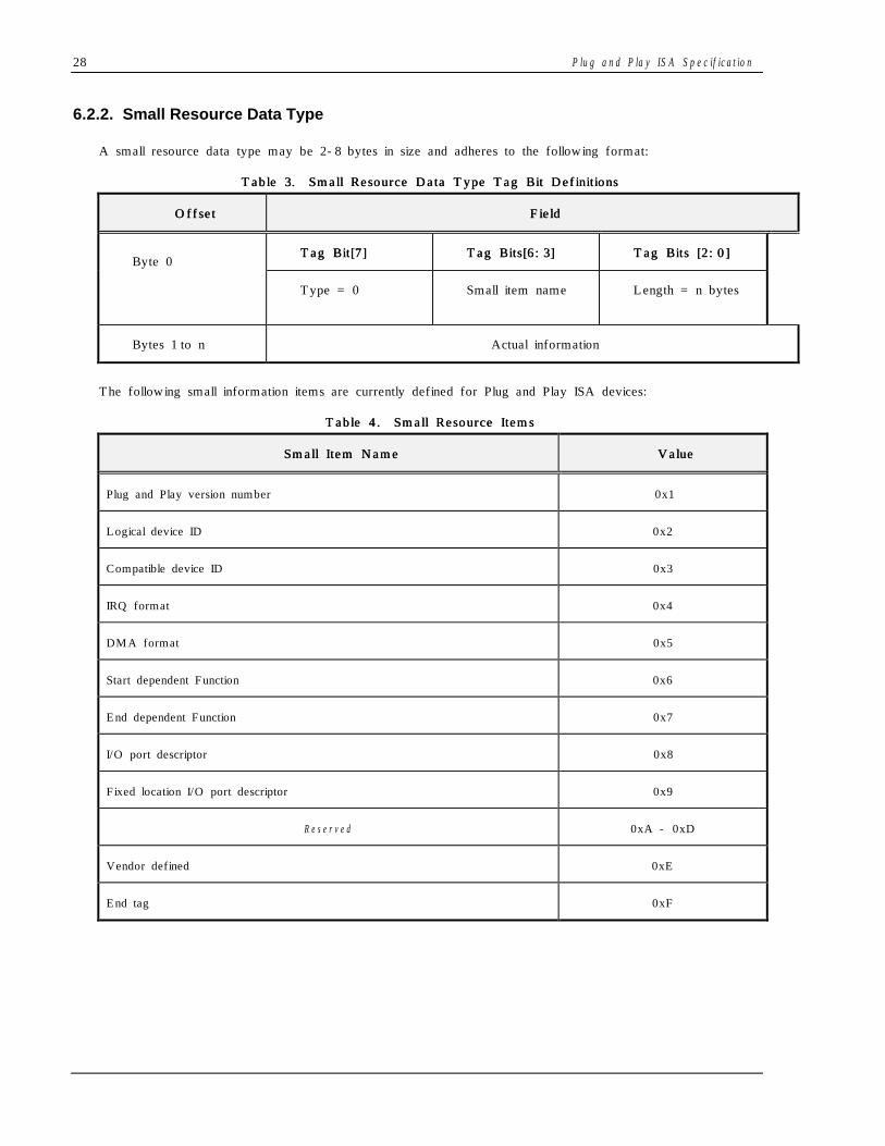
28 P lu g a n d P la y IS A S p e c if ic a t io n
6.2.2. Small Resource Data Type
A small resource data type may be 2-8 bytes in size and adheres to the following format:
Table Table 33. Small Resource Data Type Tag Bit Definitions. Small Resource Data Type Tag Bit Definitions
OffsetOffset FieldField
Byte 0Tag Bit[7]Tag Bit[7] Tag Bits[6:3]Tag Bits[6:3] Tag Bits [2:0]Tag Bits [2:0]
Type = 0 Small item name Length = n bytes
Bytes 1 to n Actual information
The following small information items are currently defined for Plug and Play ISA devices:
Table Table 44. Small Resource Items. Small Resource Items
Small Item NameSmall Item Name ValueValue
Plug and Play version number 0x1
Logical device ID 0x2
Compatible device ID 0x3
IRQ format 0x4
DMA format 0x5
Start dependent Function 0x6
End dependent Function 0x7
I/O port descriptor 0x8
Fixed location I/O port descriptor 0x9
R e s e r v e d 0xA - 0xD
Vendor defined 0xE
End tag 0xF

P lu g a n d P la y IS A S p e c if ic a t io n 29
6.2.2.1. Plug and Play Version Number
The Plug and Play Version Number identifies the version of the Plug and Play specification with which thiscard is compatible. A vendor specific version number is included and may be used by a device driver toverify the version of the card.
OffsetOffset Field NameField Name
Byte 0 Value = 00001010B (Type = 0, small item name = 0x1, length = 2)
Byte 1 Plug and Play version number (in packed BCD format, major bits[7:4], minor bits[3:0]) Example:
Version 1.0 = 0x10, Version 2.3 = 0x23, Version 2.91= 0x29
Byte 2 Vendor specific version number
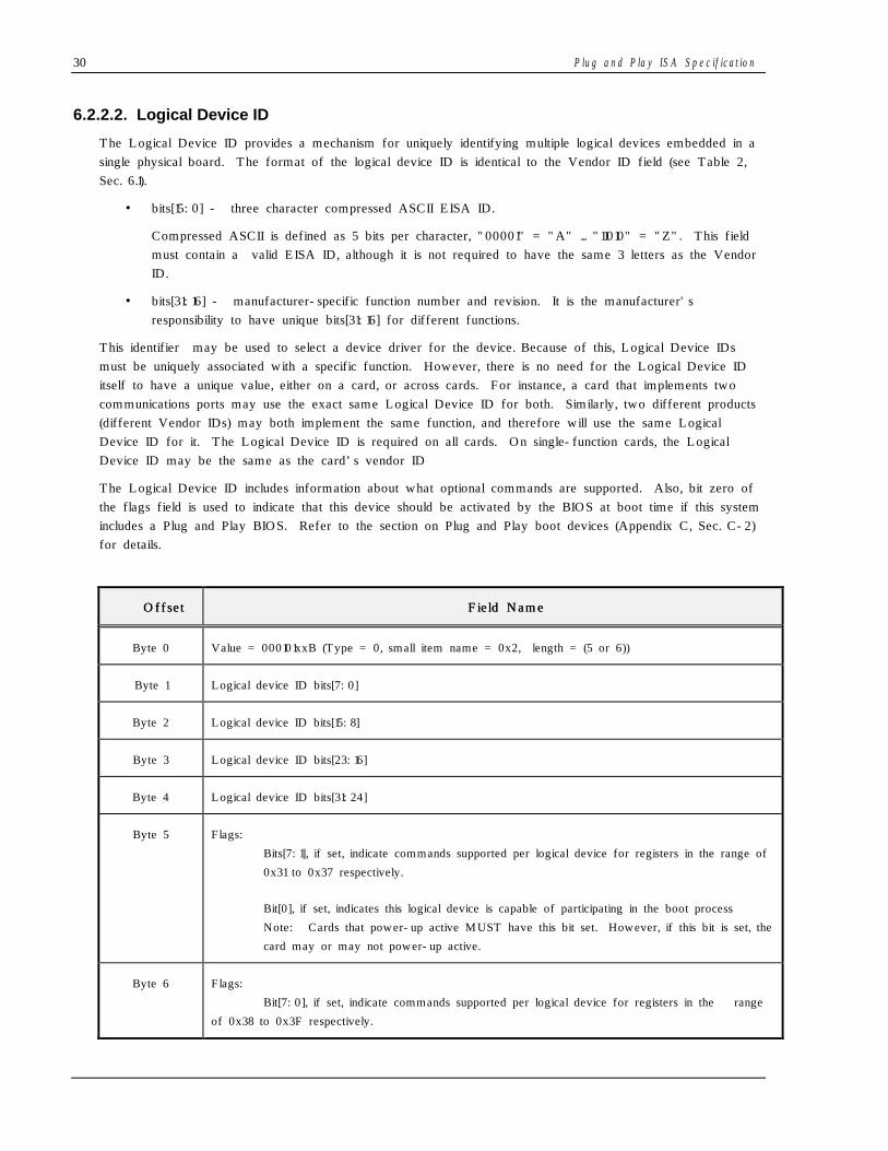
30 P lu g a n d P la y IS A S p e c if ic a t io n
6.2.2.2. Logical Device ID
The Logical Device ID provides a mechanism for uniquely identifying multiple logical devices embedded in asingle physical board. The format of the logical device ID is identical to the Vendor ID field (see Table 2,Sec. 6.1).
• bits[15:0] - three character compressed ASCII EISA ID.
Compressed ASCII is defined as 5 bits per character, "00001" = "A" ... "11010" = "Z". This fieldmust contain a valid EISA ID, although it is not required to have the same 3 letters as the VendorID.
• bits[31:16] - manufacturer-specific function number and revision. It is the manufacturer'sresponsibility to have unique bits[31:16] for different functions.
This identifier may be used to select a device driver for the device. Because of this, Logical Device IDsmust be uniquely associated with a specific function. However, there is no need for the Logical Device IDitself to have a unique value, either on a card, or across cards. For instance, a card that implements twocommunications ports may use the exact same Logical Device ID for both. Similarly, two different products(different Vendor IDs) may both implement the same function, and therefore will use the same LogicalDevice ID for it. The Logical Device ID is required on all cards. On single-function cards, the LogicalDevice ID may be the same as the card’s vendor ID
The Logical Device ID includes information about what optional commands are supported. Also, bit zero ofthe flags field is used to indicate that this device should be activated by the BIOS at boot time if this systemincludes a Plug and Play BIOS. Refer to the section on Plug and Play boot devices (Appendix C, Sec. C-2)for details.
OffsetOffset Field NameField Name
Byte 0 Value = 000101xxB (Type = 0, small item name = 0x2, length = (5 or 6))
Byte 1 Logical device ID bits[7:0]
Byte 2 Logical device ID bits[15:8]
Byte 3 Logical device ID bits[23:16]
Byte 4 Logical device ID bits[31:24]
Byte 5 Flags:
Bits[7:1], if set, indicate commands supported per logical device for registers in the range of
0x31 to 0x37 respectively.
Bit[0], if set, indicates this logical device is capable of participating in the boot process
Note: Cards that power-up active MUST have this bit set. However, if this bit is set, the
card may or may not power-up active.
Byte 6 Flags:
Bit[7:0], if set, indicate commands supported per logical device for registers in the range
of 0x38 to 0x3F respectively.
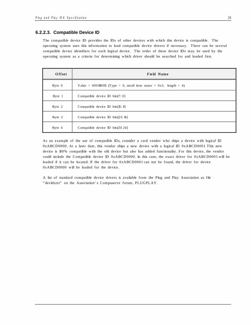
P lu g a n d P la y IS A S p e c if ic a t io n 31
6.2.2.3. Compatible Device ID
The compatible device ID provides the IDs of other devices with which this device is compatible. Theoperating system uses this information to load compatible device drivers if necessary. There can be severalcompatible device identifiers for each logical device. The order of these device IDs may be used by theoperating system as a criteria for determining which driver should be searched for and loaded first.
OffsetOffset Field NameField Name
Byte 0 Value = 00011100B (Type = 0, small item name = 0x3, length = 4)
Byte 1 Compatible device ID bits[7:0]
Byte 2 Compatible device ID bits[15:8]
Byte 3 Compatible device ID bits[23:16]
Byte 4 Compatible device ID bits[31:24]
As an example of the use of compatible IDs, consider a card vendor who ships a device with logical ID0xABCD0000. At a later date, this vendor ships a new device with a logical ID 0xABCD0001. This newdevice is 100% compatible with the old device but also has added functionality. For this device, the vendorcould include the Compatible device ID 0xABCD0000. In this case, the exact driver for 0xABCD0001 will beloaded if it can be located. If the driver for 0xABCD0001 can not be found, the driver for device0xABCD0000 will be loaded for the device.
A list of standard compatible device drivers is available from the Plug and Play Association as file“devids.txt” on the Association’s Compuserve forum, PLUGPLAY.
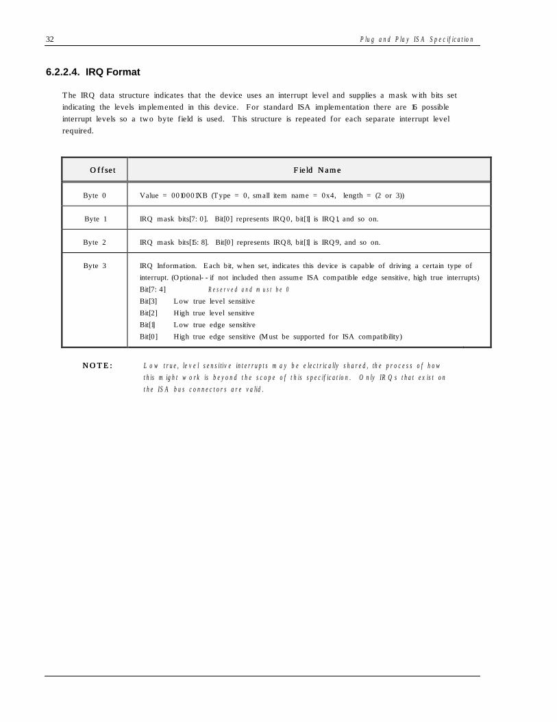
32 P lu g a n d P la y IS A S p e c if ic a t io n
6.2.2.4. IRQ Format
The IRQ data structure indicates that the device uses an interrupt level and supplies a mask with bits setindicating the levels implemented in this device. For standard ISA implementation there are 16 possibleinterrupt levels so a two byte field is used. This structure is repeated for each separate interrupt levelrequired.
OffsetOffset Field NameField Name
Byte 0 Value = 0010001XB (Type = 0, small item name = 0x4, length = (2 or 3))
Byte 1 IRQ mask bits[7:0]. Bit[0] represents IRQ0, bit[1] is IRQ1, and so on.
Byte 2 IRQ mask bits[15:8]. Bit[0] represents IRQ8, bit[1] is IRQ9, and so on.
Byte 3 IRQ Information. Each bit, when set, indicates this device is capable of driving a certain type of
interrupt. (Optional--if not included then assume ISA compatible edge sensitive, high true interrupts)
Bit[7:4] R e s e r v e d a n d m u s t b e 0
Bit[3] Low true level sensitive
Bit[2] High true level sensitive
Bit[1] Low true edge sensitive
Bit[0] High true edge sensitive (Must be supported for ISA compatibility)
NOTE:NOTE: L o w t r u e , le v e l s e n s itiv e in t e r r u p t s m a y b e e le c t r ic a lly s h a r e d , th e p r o c e s s o f h o wt h is m ig h t w o r k is b e y o n d t h e s c o p e o f t h is s p e c if ic a t io n . O n ly IR Q s t h a t e x is t o nt h e IS A b u s c o n n e c t o r s a r e v a lid .

P lu g a n d P la y IS A S p e c if ic a t io n 33
6.2.2.5. DMA Format
The DMA data structure indicates that the device uses a DMA channel and supplies a mask with bits setindicating the channels actually implemented in this device. This structure is repeated for each separatechannel required.
OffsetOffset Field NameField Name
Byte 0 Value = 00101010B (Type = 0, small item name = 0x5, length = 2)
Byte 1 DMA channel mask bits[7:0]. Bit[0] is channel 0.
Byte 2 Bit[7] R e s e r v e d a n d m u s t b e 0
Bits[6:5] DMA channel speed supported
Status
00 Indicates compatibility mode
01 Indicates Type A DMA as described in the EISA Specification
10 Indicates Type B DMA
11 Indicates Type F
Bit[4] DMA word mode
Status
0 DMA may not execute in count by word mode
1 DMA may execute in count by word mode
Bit[3] DMA byte mode status
Status
0 DMA may not execute in count by byte mode
1 DMA may execute in count by byte mode
Bit[2] Logical device bus master status
Status
0 Logical device is not a bus master
1 Logical device is a bus master
Bits[1:0] DMA transfer type preference
Status
00 8-bit only
01 8- and 16-bit
10 16-bit only
11 R e s e r v e d
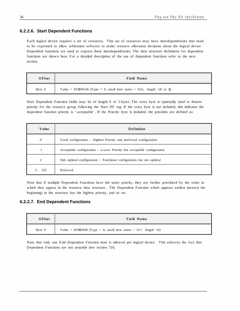
34 P lu g a n d P la y IS A S p e c if ic a t io n
6.2.2.6. Start Dependent Functions
Each logical device requires a set of resources. This set of resources may have interdependencies that needto be expressed to allow arbitration software to make resource allocation decisions about the logical device.Dependent functions are used to express these interdependencies. The data structure definitions for dependentfunctions are shown here. For a detailed description of the use of dependent functions refer to the nextsection.
OffsetOffset Field NameField Name
Byte 0 Value = 0011000xB (Type = 0, small item name = 0x6, length =(0 or 1))
Start Dependent Function fields may be of length 0 or 1 bytes. The extra byte is optionally used to denotepriority for the resource group following the Start DF tag. If the extra byte is not included, this indicates thedependent function priority is ‘acceptable’. If the Priority byte is included, the priorities are defined as:
ValueValue DefinitionDefinition
0 Good configuration - Highest Priority and preferred configuration
1 Acceptable configuration - Lower Priority but acceptable configuration
2 Sub-optimal configuration - Functional configuration but not optimal
3 - 255 Reserved
Note that if multiple Dependent Functions have the same priority, they are further prioritized by the order inwhich they appear in the resource data structure. The Dependent Function which appears earliest (nearest thebeginning) in the structure has the highest priority, and so on.
6.2.2.7. End Dependent Functions
OffsetOffset Field NameField Name
Byte 0 Value = 00111000B (Type = 0, small item name = 0x7 length =0)
Note that only one End Dependent Function item is allowed per logical device. This enforces the fact thatDependent Functions are not nestable (see section 7.0).
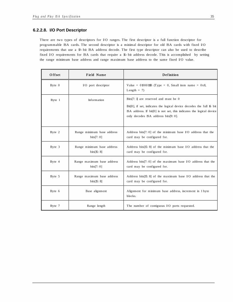
P lu g a n d P la y IS A S p e c if ic a t io n 35
6.2.2.8. I/O Port Descriptor
There are two types of descriptors for I/O ranges. The first descriptor is a full function descriptor forprogrammable ISA cards. The second descriptor is a minimal descriptor for old ISA cards with fixed I/Orequirements that use a 10-bit ISA address decode. The first type descriptor can also be used to describefixed I/O requirements for ISA cards that require a 16-bit address decode. This is accomplished by settingthe range minimum base address and range maximum base address to the same fixed I/O value.
OffsetOffset Field NameField Name DefinitionDefinition
Byte 0 I/O port descriptor Value = 01000111B (Type = 0, Small item name = 0x8,
Length = 7)
Byte 1 Information Bits[7:1] are reserved and must be 0
Bit[0], if set, indicates the logical device decodes the full 16 bit
ISA address. If bit[0] is not set, this indicates the logical device
only decodes ISA address bits[9:0].
Byte 2 Range minimum base address
bits[7:0]
Address bits[7:0] of the minimum base I/O address that the
card may be configured for.
Byte 3 Range minimum base address
bits[15:8]
Address bits[15:8] of the minimum base I/O address that the
card may be configured for.
Byte 4 Range maximum base address
bits[7:0]
Address bits[7:0] of the maximum base I/O address that the
card may be configured for.
Byte 5 Range maximum base address
bits[15:8]
Address bits[15:8] of the maximum base I/O address that the
card may be configured for.
Byte 6 Base alignment Alignment for minimum base address, increment in 1 byte
blocks.
Byte 7 Range length The number of contiguous I/O ports requested.
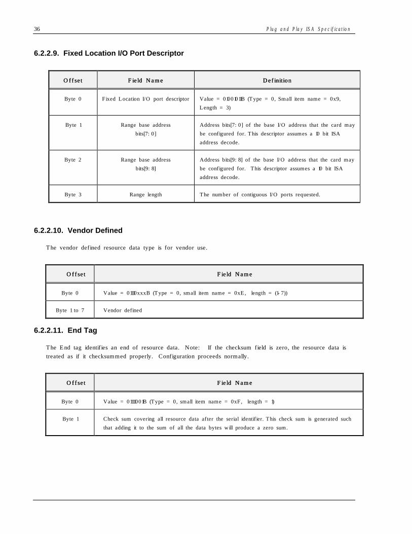
36 P lu g a n d P la y IS A S p e c if ic a t io n
6.2.2.9. Fixed Location I/O Port Descriptor
OffsetOffset Field NameField Name DefinitionDefinition
Byte 0 Fixed Location I/O port descriptor Value = 01001011B (Type = 0, Small item name = 0x9,
Length = 3)
Byte 1 Range base address
bits[7:0]
Address bits[7:0] of the base I/O address that the card may
be configured for. This descriptor assumes a 10 bit ISA
address decode.
Byte 2 Range base address
bits[9:8]
Address bits[9:8] of the base I/O address that the card may
be configured for. This descriptor assumes a 10 bit ISA
address decode.
Byte 3 Range length The number of contiguous I/O ports requested.
6.2.2.10. Vendor Defined
The vendor defined resource data type is for vendor use.
OffsetOffset Field NameField Name
Byte 0 Value = 01110xxxB (Type = 0, small item name = 0xE, length = (1-7))
Byte 1 to 7 Vendor defined
6.2.2.11. End Tag
The End tag identifies an end of resource data. Note: If the checksum field is zero, the resource data istreated as if it checksummed properly. Configuration proceeds normally.
OffsetOffset Field NameField Name
Byte 0 Value = 01111001B (Type = 0, small item name = 0xF, length = 1)
Byte 1 Check sum covering all resource data after the serial identifier. This check sum is generated such
that adding it to the sum of all the data bytes will produce a zero sum.
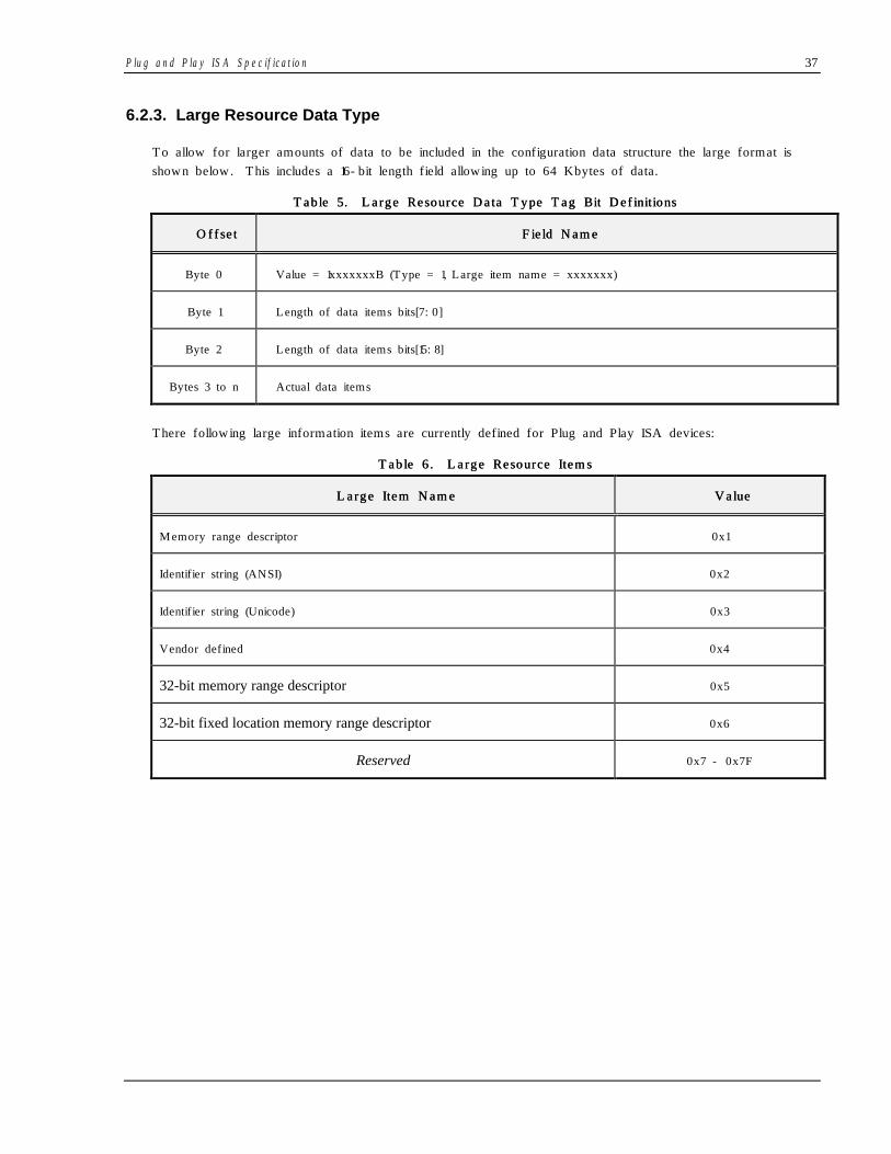
P lu g a n d P la y IS A S p e c if ic a t io n 37
6.2.3. Large Resource Data Type
To allow for larger amounts of data to be included in the configuration data structure the large format isshown below. This includes a 16-bit length field allowing up to 64 Kbytes of data.
Table 5. Large Resource Data Type Tag Bit DefinitionsTable 5. Large Resource Data Type Tag Bit Definitions
OffsetOffset Field NameField Name
Byte 0 Value = 1xxxxxxxB (Type = 1, Large item name = xxxxxxx)
Byte 1 Length of data items bits[7:0]
Byte 2 Length of data items bits[15:8]
Bytes 3 to n Actual data items
There following large information items are currently defined for Plug and Play ISA devices:
Table 6. Large Resource ItemsTable 6. Large Resource Items
Large Item NameLarge Item Name ValueValue
Memory range descriptor 0x1
Identifier string (ANSI) 0x2
Identifier string (Unicode) 0x3
Vendor defined 0x4
32-bit memory range descriptor 0x5
32-bit fixed location memory range descriptor 0x6
Reserved 0x7 - 0x7F

38 P lu g a n d P la y IS A S p e c if ic a t io n
6.2.3.1. Memory Range Descriptor
SizeSize Field NameField Name DefinitionDefinition
Byte Memory range descriptor Value = 10000001B (Type = 1, Large item name = 1)
Byte Length, bits[7:0] Value = 00001001B (9)
Byte Length, bits[15:8] Value = 00000000B
Byte Information This field provides extra information about this memory.
Bit[7] Reserved and must be 0Bit[6] Memory is an expansion ROMBit[5] Memory is shadowable.Bits[4:3] Memory control.
Status00 8-bit memory only01 16-bit memory only10 8- and 16-bit supported.11 Reserved
Bit[2] Support typeStatus
1 decode supports high address0 decode supports range length.
Bit[1] Cache support typeStatus
1 read cacheable, write-through0 non-cacheable.
Bit[0] Write statusStatus
1 writeable0 non-writeable (ROM)
(continued on next page)
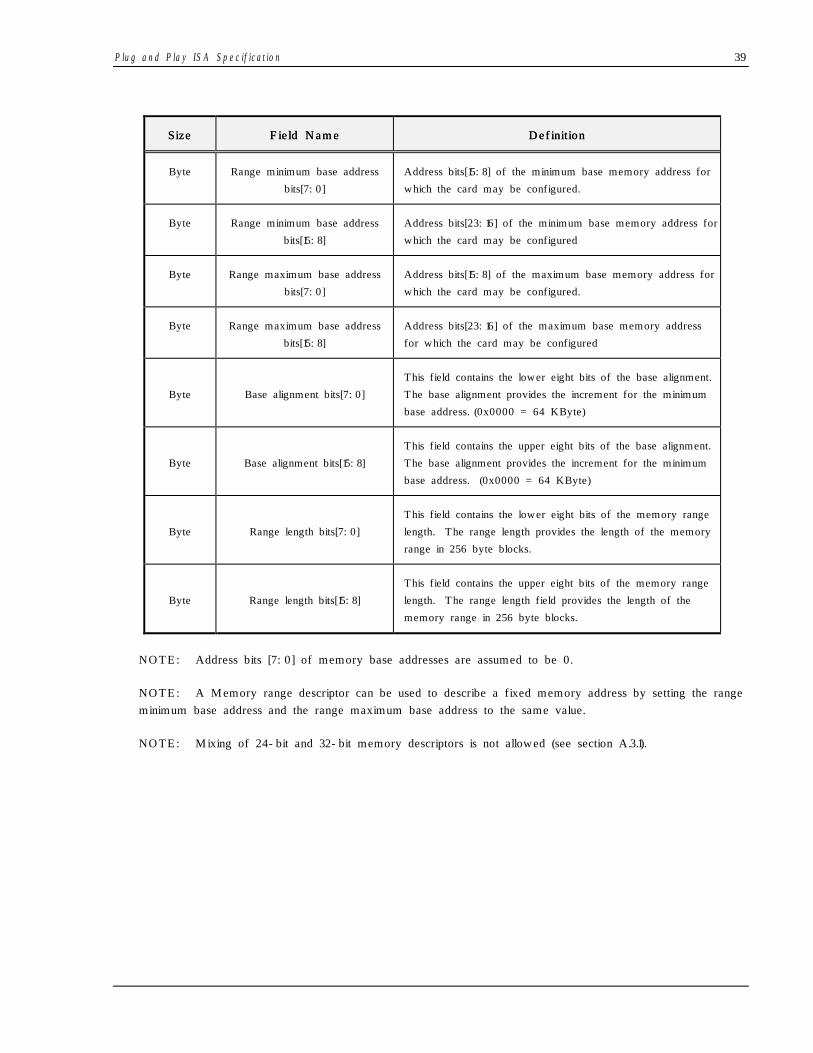
P lu g a n d P la y IS A S p e c if ic a t io n 39
SizeSize Field NameField Name DefinitionDefinition
Byte Range minimum base address
bits[7:0]
Address bits[15:8] of the minimum base memory address for
which the card may be configured.
Byte Range minimum base address
bits[15:8]
Address bits[23:16] of the minimum base memory address for
which the card may be configured
Byte Range maximum base address
bits[7:0]
Address bits[15:8] of the maximum base memory address for
which the card may be configured.
Byte Range maximum base address
bits[15:8]
Address bits[23:16] of the maximum base memory address
for which the card may be configured
Byte Base alignment bits[7:0]
This field contains the lower eight bits of the base alignment.
The base alignment provides the increment for the minimum
base address. (0x0000 = 64 KByte)
Byte Base alignment bits[15:8]
This field contains the upper eight bits of the base alignment.
The base alignment provides the increment for the minimum
base address. (0x0000 = 64 KByte)
Byte Range length bits[7:0]
This field contains the lower eight bits of the memory range
length. The range length provides the length of the memory
range in 256 byte blocks.
Byte Range length bits[15:8]
This field contains the upper eight bits of the memory range
length. The range length field provides the length of the
memory range in 256 byte blocks.
NOTE: Address bits [7:0] of memory base addresses are assumed to be 0.
NOTE: A Memory range descriptor can be used to describe a fixed memory address by setting the rangeminimum base address and the range maximum base address to the same value.
NOTE: Mixing of 24-bit and 32-bit memory descriptors is not allowed (see section A.3.1).

40 P lu g a n d P la y IS A S p e c if ic a t io n
6.2.3.2. ANSI Identifier String
SizeSize Field NameField Name DefinitionDefinition
Byte Identifier string Value = 10000010B (Type = 1, Large item name = 2)
Byte Length, bits[7:0] Lower eight bits of identifier string length
Byte Length, bits[15:8] Upper eight bits of identifier string length
N * bytes Identifier string Device description as an ANSI string
The identifier string is 8-bit ANSI. The length of the string is defined in the structure so the string does notneed to be zero terminated. Display software will insure the proper termination gets added to the string sothat the termination byte does not need to be stored in the card's non-volatile storage. Each card is requiredto have an identifier string, each logical device may optionally have an identifier string.
6.2.3.3. Unicode Identifier String
SizeSize Field NameField Name DefinitionDefinition
Byte Identifier string Value = 10000011B (Type = 1, Large item name = 3)
Byte Length, bits[7:0] Lower eight bits of length of string plus four
Byte Length, bits[15:8] Upper eight bits of length of string plus four
Byte Country identifier, bits[7:0] T o b e d e t e r m in e d
Byte Country identifier, bits[15:8] T o b e d e t e r m in e d
N * bytes Identifier string Device description characters
Currently, only ANSI identifier strings are defined. The definition for Unicode will be added at a later time.

P lu g a n d P la y IS A S p e c if ic a t io n 41
6.2.3.4. Vendor Defined
The vendor defined resource data type is for vendor use.
SizeSize Field NameField Name DefinitionDefinition
Byte Vendor defined Value = 10000100B (Type = 1, Large item name = 4)
Byte Length, bits[7:0] Lower eight bits of vendor defined data
Byte Length, bits[15:8] Upper eight bits of vendor defined data
N * bytes Vendor Defined Vendor defined data bytes
6.2.3.5. 32-bit Memory Range Descriptor
SizeSize Field NameField Name DefinitionDefinition
Byte Memory range descriptor Value = 10000101B (Type = 1, Large item name = 5)
Byte Length, bits[7:0] Value = 00010001B (17)
Byte Length, bits[15:8] Value = 00000000B
Byte Information This field provides extra information about this memory.
Bit[7] Reserved and must be 0Bit[6] Memory is an expansion ROMBit[5] Memory is shadowable.Bits[4:3] Memory control.
Status00 8-bit memory only01 16-bit memory only10 8- and 16-bit supported.11 32-bit memory only
Bit[2] Support typeStatus
1 decode supports high address0 decode supports range length
Bit[1] Cache support typeStatus
1 read cacheable, write-through0 non-cacheable.
Bit[0] Write statusStatus
1 writeable0 non-writeable (ROM)
(continued on next page)

42 P lu g a n d P la y IS A S p e c if ic a t io n
SizeSize Field NameField Name DefinitionDefinition
Byte Range minimum base address
bits[7:0]
Address bits[7:0] of the minimum base memory address for
which the card may be configured.
Byte Range minimum base address
bits[15:8]
Address bits[15:8] of the minimum base memory address for
which the card may be configured
Byte Range minimum base address
bits[23:16]
Address bits[23:16] of the minimum base memory address for
which the card may be configured.
Byte Range minimum base address
bits[31:24]
Address bits[31:24] of the minimum base memory address for
which the card may be configured
Byte Range maximum base address
bits[7:0]
Address bits[7:0] of the maximum base memory address for
which the card may be configured.
Byte Range maximum base address
bits[15:8]
Address bits[15:8] of the maximum base memory address for
which the card may be configured
Byte Range maximum base address
bits[23:16]
Address bits[23:16] of the maximum base memory address
for which the card may be configured.
Byte Range maximum base address
bits[31:24]
Address bits[31:24] of the maximum base memory address
for which the card may be configured
Byte Base alignment bits[7:0]
This field contains Bits[7:0] of the base alignment. The base
alignment provides the increment for the minimum base
address.
Byte Base alignment bits[15:8]
This field contains Bits[15:8] of the base alignment. The base
alignment provides the increment for the minimum base
address.
Byte Base alignment bits[23:16]
This field contains Bits[23:16] of the base alignment. The
base alignment provides the increment for the minimum base
address.
(continued on next page)

P lu g a n d P la y IS A S p e c if ic a t io n 43
SizeSize Field NameField Name DefinitionDefinition
Byte Base alignment bits[31:24]
This field contains Bits[31:24] of the base alignment. The
base alignment provides the increment for the minimum base
address.
Byte Range length bits[7:0]
This field contains Bits[7:0] of the memory range length.
The range length provides the length of the memory range in
1 byte blocks.
Byte Range length bits[15:8]
This field contains Bits[15:8] of the memory range length.
The range length provides the length of the memory range in
1 byte blocks.
Byte Range length bits[23:16]
This field contains Bits[23:16] of the memory range length.
The range length provides the length of the memory range in
1 byte blocks.
Byte Range length bits[31:24]
This field contains Bits[31:24] of the memory range length.
The range length provides the length of the memory range in
1 byte blocks.
NOTE: Mixing of 24-bit and 32-bit memory descriptors is not allowed (see section A.3.1).

44 P lu g a n d P la y IS A S p e c if ic a t io n
6.2.3.6. 32-bit Fixed Location Memory Range Descriptor
SizeSize Field NameField Name DefinitionDefinition
Byte Memory range descriptor Value = 10000110B (Type = 1, Large item name = 6)
Byte Length, bits[7:0] Value = 00001001B (9)
Byte Length, bits[15:8] Value = 00000000B
Byte Information This field provides extra information about this memory.
Bit[7] Reserved and must be 0Bit[6] Memory is an expansion ROMBit[5] Memory is shadowable.Bits[4:3] Memory control.
Status00 8-bit memory only01 16-bit memory only10 8- and 16-bit supported.11 32-bit memory only
Bit[2] Support typeStatus
1 decode supports high address0 decode supports range length
Bit[1] Cache support typeStatus
1 read cacheable, write-through0 non-cacheable.
Bit[0] Write statusStatus
1 writeable0 non-writeable (ROM)
(continued on next page)
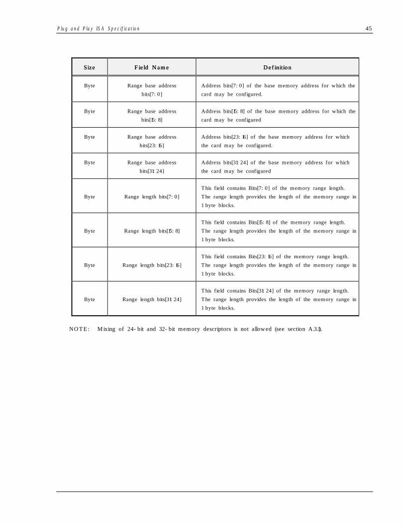
P lu g a n d P la y IS A S p e c if ic a t io n 45
SizeSize Field NameField Name DefinitionDefinition
Byte Range base address
bits[7:0]
Address bits[7:0] of the base memory address for which the
card may be configured.
Byte Range base address
bits[15:8]
Address bits[15:8] of the base memory address for which the
card may be configured
Byte Range base address
bits[23:16]
Address bits[23:16] of the base memory address for which
the card may be configured.
Byte Range base address
bits[31:24]
Address bits[31:24] of the base memory address for which
the card may be configured
Byte Range length bits[7:0]
This field contains Bits[7:0] of the memory range length.
The range length provides the length of the memory range in
1 byte blocks.
Byte Range length bits[15:8]
This field contains Bits[15:8] of the memory range length.
The range length provides the length of the memory range in
1 byte blocks.
Byte Range length bits[23:16]
This field contains Bits[23:16] of the memory range length.
The range length provides the length of the memory range in
1 byte blocks.
Byte Range length bits[31:24]
This field contains Bits[31:24] of the memory range length.
The range length provides the length of the memory range in
1 byte blocks.
NOTE: Mixing of 24-bit and 32-bit memory descriptors is not allowed (see section A.3.1).
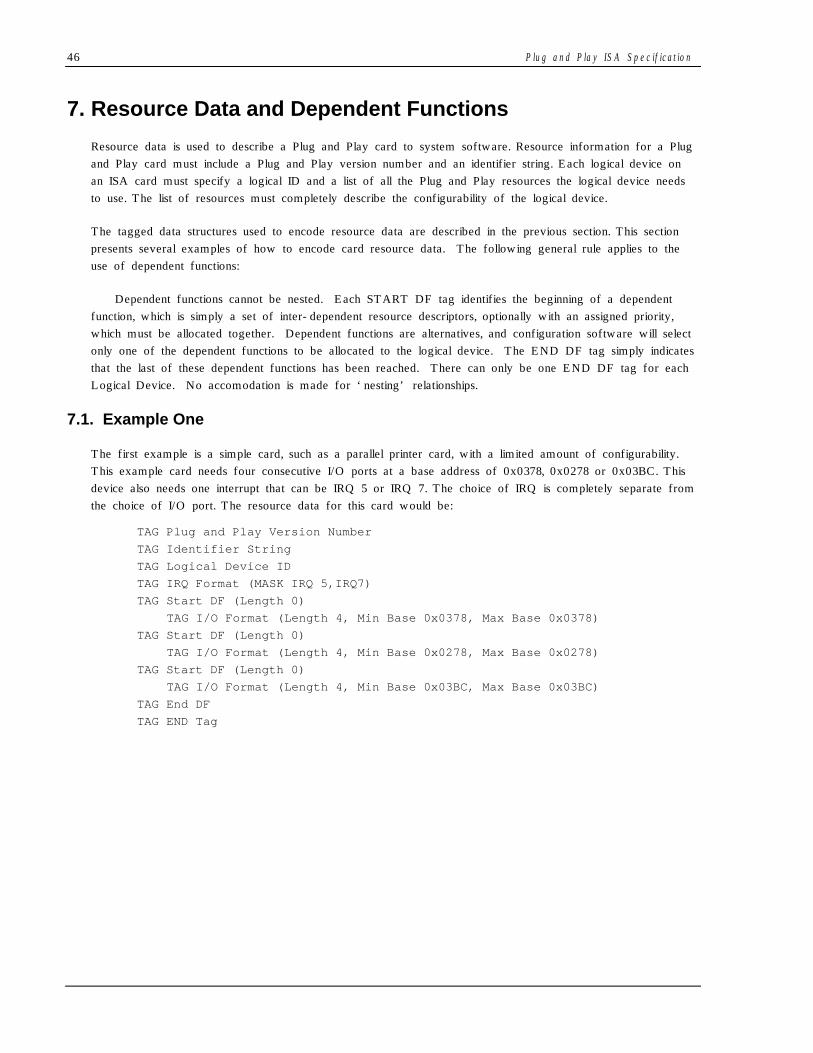
46 P lu g a n d P la y IS A S p e c if ic a t io n
7. Resource Data and Dependent Functions
Resource data is used to describe a Plug and Play card to system software. Resource information for a Plugand Play card must include a Plug and Play version number and an identifier string. Each logical device onan ISA card must specify a logical ID and a list of all the Plug and Play resources the logical device needsto use. The list of resources must completely describe the configurability of the logical device.
The tagged data structures used to encode resource data are described in the previous section. This sectionpresents several examples of how to encode card resource data. The following general rule applies to theuse of dependent functions:
Dependent functions cannot be nested. Each START DF tag identifies the beginning of a dependentfunction, which is simply a set of inter-dependent resource descriptors, optionally with an assigned priority,which must be allocated together. Dependent functions are alternatives, and configuration software will selectonly one of the dependent functions to be allocated to the logical device. The END DF tag simply indicatesthat the last of these dependent functions has been reached. There can only be one END DF tag for eachLogical Device. No accomodation is made for ‘nesting’ relationships.
7.1. Example One
The first example is a simple card, such as a parallel printer card, with a limited amount of configurability.This example card needs four consecutive I/O ports at a base address of 0x0378, 0x0278 or 0x03BC. Thisdevice also needs one interrupt that can be IRQ 5 or IRQ 7. The choice of IRQ is completely separate fromthe choice of I/O port. The resource data for this card would be:
TAG Plug and Play Version Number
TAG Identifier String
TAG Logical Device ID
TAG IRQ Format (MASK IRQ 5,IRQ7)
TAG Start DF (Length 0)
TAG I/O Format (Length 4, Min Base 0x0378, Max Base 0x0378)
TAG Start DF (Length 0)
TAG I/O Format (Length 4, Min Base 0x0278, Max Base 0x0278)
TAG Start DF (Length 0)
TAG I/O Format (Length 4, Min Base 0x03BC, Max Base 0x03BC)
TAG End DF
TAG END Tag

P lu g a n d P la y IS A S p e c if ic a t io n 47
7.2. Example Two
Dependent functions can be used to express relationships between resources that are interdependent. Forexample, consider a card that may be configured to use I/O Port 0x0300 and IRQ 5 or I/O Port 0x0310and IRQ 7, this device has the following resource data structure:
TAG Plug and Play Version Number
TAG Identifier String
TAG Logical Device ID
TAG Start DF (Length 0)
TAG I/O Format (Length 4, Min Base 0x0300, Max Base 0x0300)
TAG IRQ Format (MASK IRQ 5)
TAG Start DF (Length 0)
TAG I/O Format (Length 4, Min Base 0x0310, Max Base 0x0310)
TAG IRQ Format (MASK IRQ 7)
TAG End DF
TAG END Tag
7.3. Example Three
Dependent functions can also be used to express the priority of configuration options. For example consider acard that performs DMA using a memory buffer if memory space is available. Alternatively, the card uses aDMA channel if no memory resources are available. This example card needs 16 consecutive I/O ports thatmay be located anywhere in the range of 0x300 to 0x3F0. The card needs one interrupt that can be eitherIRQ 5,7,10,11,12. The card needs a 128 KByte memory window, if that is not available it can use a 64 KBytememory window and if that is not available, it will run using a DMA channel. It supports DMA channels5,6,7. This device has the following resource data structure:
TAG Plug and Play Version Number
TAG Identifier String
TAG Logical Device ID
TAG I/O Format (Length 16, Min Base 0x0300, Max Base 0x03F0)
TAG IRQ Format (MASK IRQ 5,7,10,11,12)
TAG Start DF (Length 1) (Priority 0)
TAG Memory Format (Length = 128K, Min Base 0x0C0000, Max Base 0x0E0000)
TAG DMA Format (MASK no DMA channel)
TAG Start DF (Length 1) (Priority 1)
TAG Memory Format (Length = 64K, Min Base 0x0C0000, Max Base 0x0E0000)
TAG DMA Format (MASK no DMA channel)
TAG Start DF (Length 1) (Priority 2)
TAG Memory Format (Length = 0, Min Base 0x0C0000, Max Base 0x0E0000)
TAG DMA Format (MASK 5,6,7)
TAG End DF
TAG END Tag
7.4. Example Four
The following example shows an ILLEGAL use of Dependent Functions. The structure below includes twoEND DF tags, which is not allowed.
48 P lu g a n d P la y IS A S p e c if ic a t io n
TAG Plug and Play Version Number
TAG Identifier String
TAG Logical Device ID
TAG IRQ Format (MASK IRQ 5,IRQ7)
TAG Start DF (Length 0)
TAG I/O Format (Length 4, Min Base 0x0378, Max Base 0x0378)
TAG Start DF (Length 0)
TAG I/O Format (Length 4, Min Base 0x0278, Max Base 0x0278)
TAG Start DF (Length 0)
TAG I/O Format (Length 4, Min Base 0x03BC, Max Base 0x03BC)
TAG End DF
TAG Start DF (Length 1 - Priority 1)
TAG DMA Format (MASK no DMA channel)
TAG Start DF (Length 1 - Priority 2)
TAG DMA Format (MASK 5,6,7)
TAG End DF
TAG END Tag
The correct structure is:
TAG Plug and Play Version Number
TAG Identifier String
TAG Logical Device ID
TAG IRQ Format (MASK IRQ 5,IRQ7)
TAG Start DF (Length 0)
TAG I/O Format (Length 4, Min Base 0x0378, Max Base 0x0378)
TAG DMA Format (MASK no DMA channel)
TAG Start DF (Length 0)
TAG I/O Format (Length 4, Min Base 0x0278, Max Base 0x0278)
TAG DMA Format (MASK no DMA channel)
TAG Start DF (Length 0)
TAG I/O Format (Length 4, Min Base 0x03BC, Max Base 0x03BC)
TAG DMA Format (MASK no DMA channel)
TAG Start DF (Length 1 - Priority 2)
TAG I/O Format (Length 4, Min Base 0x0378, Max Base 0x0378)
TAG DMA Format (MASK 5,6,7)
TAG Start DF (Length 1 - Priority 2)
TAG I/O Format (Length 4, Min Base 0x0278, Max Base 0x0278)
TAG DMA Format (MASK 5,6,7)
TAG Start DF (Length 1 - Priority 2)
TAG I/O Format (Length 4, Min Base 0x03BC, Max Base 0x03BC)
TAG DMA Format (MASK 5,6,7)
TAG End DF
TAG END Tag
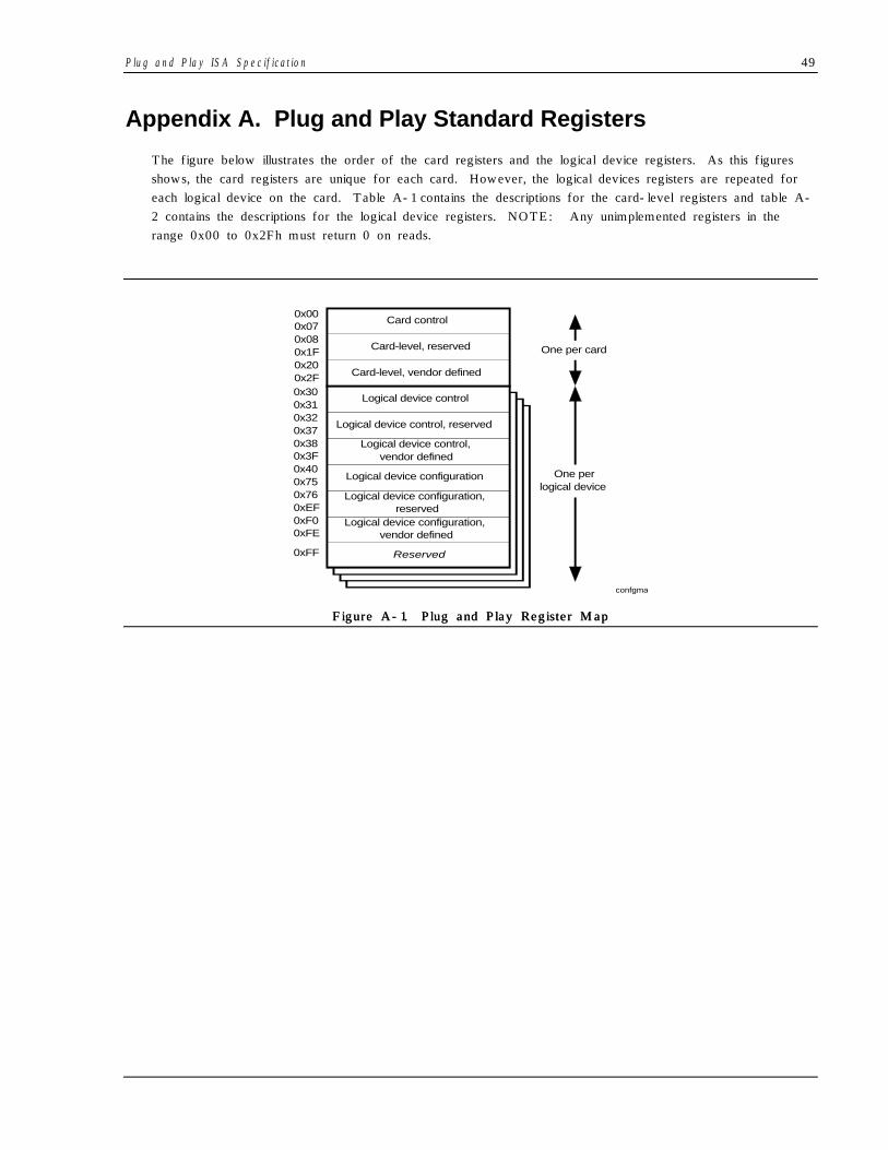
P lu g a n d P la y IS A S p e c if ic a t io n 49
Appendix A. Plug and Play Standard Registers
The figure below illustrates the order of the card registers and the logical device registers. As this figuresshows, the card registers are unique for each card. However, the logical devices registers are repeated foreach logical device on the card. Table A-1 contains the descriptions for the card-level registers and table A-2 contains the descriptions for the logical device registers. NOTE: Any unimplemented registers in therange 0x00 to 0x2Fh must return 0 on reads.
confgmap
Card control0x000x070x080x1F0x200x2F Card-level, vendor defined
One perlogical device
One per cardCard-level, reserved
Logical device control
Logical device control, reserved
Logical device control,vendor defined
Logical device configuration
Logical device configuration,reserved
Logical device configuration,vendor defined
Reserved
0x300x310x320x370x380x3F0x400x750x760xEF0xF00xFE
0xFF
Figure AFigure A--11 . Plug and Play Register Map. Plug and Play Register Map

50 P lu g a n d P la y IS A S p e c if ic a t io n
A.1. Plug and Play Card Control Registers
Table ATable A--11 . . Plug and Play Standard RegistersPlug and Play Standard Registers
NameName Address PortAddress PortValueValue
DefinitionDefinition
Set RD_DATA Port 0x00 Writing to this location modifies the address of the port
used for reading from the Plug and Play ISA cards.
Bits[7:0] become I/O read port address bits[9:2]. Reads
from this register are ignored.
Serial Isolation 0x01 A read to this register causes a Plug and Play cards in the
I s o l a t i o nI s o l a t i o n state to compare one bit of the boards ID. This
process is fully described above. This register is read only.
Config Control 0x02 Bit[2] - Reset CSN to 0
Bit [1] - Return to the Wait for Key state
Bit[0] - Reset all logical devices and restoreconfiguration registers to their power-up values.
A write to bit[0] of this register performs a resetfunction on all logical devices. This resets the contentsof configuration registers to their default state. Allcard's logical devices enter their default state and theCSN is preserved.
A write to bit[1] of this register causes all cards to enterthe Wait for Key state but all CSNs are preserved andlogical devices are not affected.
A write to bit[2] of this register causes all cards to resettheir CSN to zero .
This register is write-only. The values are not sticky,that is, hardware will automatically clear them andthere is no need for software to clear the bits.
(continued on next page)
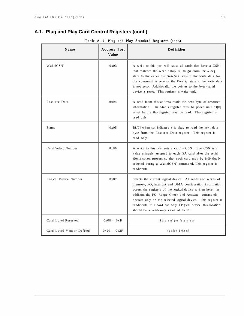
P lu g a n d P la y IS A S p e c if ic a t io n 51
A.1. Plug and Play Card Control Registers (cont.)
Table ATable A--11 . Plug and Play Standard Registers (cont.). Plug and Play Standard Registers (cont.)
NameName Address PortAddress PortValueValue
DefinitionDefinition
Wake[CSN] 0x03 A write to this port will cause all cards that have a CSN
that matches the write data[7:0] to go from the S l e e pS l e e p
state to the either the I s o l a t i o nI s o l a t i o n state if the write data for
this command is zero or the C o n f i gC o n f i g state if the write data
is not zero. Additionally, the pointer to the byte-serial
device is reset. This register is write-only.
Resource Data 0x04 A read from this address reads the next byte of resource
information. The Status register must be polled until bit[0]
is set before this register may be read. This register is
read only.
Status 0x05 Bit[0] when set indicates it is okay to read the next data
byte from the Resource Data register. This register is
read-only.
Card Select Number 0x06 A write to this port sets a card's CSN. The CSN is a
value uniquely assigned to each ISA card after the serial
identification process so that each card may be individually
selected during a Wake[CSN] command. This register is
read/write.
Logical Device Number 0x07 Selects the current logical device. All reads and writes of
memory, I/O, interrupt and DMA configuration information
access the registers of the logical device written here. In
addition, the I/O Range Check and Activate commands
operate only on the selected logical device. This register is
read/write. If a card has only 1 logical device, this location
should be a read-only value of 0x00.
Card Level Reserved 0x08 - 0x1F R e s e r v e d f o r f u t u r e u s e
Card Level, Vendor Defined 0x20 - 0x2F V e n d o r d e f in e d

52 P lu g a n d P la y IS A S p e c if ic a t io n
A.2 Plug and Play Logical Device Control Registers
Table ATable A--22. Plug and Play Logical Device Control Registers. Plug and Play Logical Device Control Registers
NameName Address PortAddress PortValueValue
DefinitionDefinition
Activate 0x30 For each logical device there is one activate register that
controls whether or not the logical device is active on the
ISA bus. Bit[0], if set, activates the logical device. Bits[7:1]
are reserved and must return 0 on reads. This is a
read/write register. Before a logical device is activated, I/O
range check must be disabled.
I/O Range Check 0x31 This register is used to perform a conflict check on the I/O
port range programmed for use by a logical device.
Bit[7:2] Reserved and must return 0 on reads
Bit[1] Enable I/O Range check, if set then I/O Range
Check is enabled. I/O range check is only valid when the
logical device is inactive.
Bit[0], if set, forces the logical device to respond to I/O
reads of the logical device's assigned I/O range with a
0x55 when I/O range check is in operation. If clear, the
logical device drives 0xAA. This register is read/write.
Logical Device Control Reserved 0x32 - 0x37 R e s e r v e d f o r f u t u r e u s e
Logical Device Control Vendor
Defined
0x38 - 0x3F V e n d o r d e f in e d r e g is t e r s

P lu g a n d P la y IS A S p e c if ic a t io n 53
A.3. Plug and Play Logical Device Configuration Registers
The resource assignments of Plug and Play cards is programmed through the address and command/dataport in the same method used for issuing commands. The following registers define memory, I/O, interruptand DMA resources used by Plug and Play cards. These configuration registers are all based on the currentlogical device selected. These configuration registers are all read/write so all current configuration informationmay be read from a card.
A.3.1. Memory Configuration Registers
Table A-3 provides a description of how memory resources are programmed. If the configuration softwaredid not allocate memory for any reason, then the memory resource registers (for example, 0x40, 0x41, 0x43,and 0x44 for descriptor 0) are written with a zero value. This disables the memory range.
There are a maximum of four memory descriptors available per logical device.
Memory range length registers are defined as a mask of address bits[23:8] (or [31:0] for 32-bit memoryspace). If a bit in the mask is set, then this indicates that memory address bit is used in a comparator todetermine an address match. If a bit is clear, this indicates that memory address bit is not used indetermining an address match. For example, a logical device that requests 64 KBytes of memory wouldhave a Range Length of:
Memory range length [23:16] = 0xFF
Memory range length [15:8] = 0x00
This indicates that address bits[23:16] are used to compare for a matching address, address bits[15:8] andbits[7:0] are not used. This 64 KByte address range must be aligned on a 64 KByte or higher boundary.
Memory upper limit registers are defined as being one byte greater than the memory resource assigned. Forexample, a logical device that requests 64 Kbytes of memory that is assigned at a base address of 1 Mbytewould have:
Memory base [23:16] = 0x10
Memory base [15:8] = 0x00
Memory upper limit [23:16] = 0x11
Memory upper limit [15:8] = 0x00
The memory control register, 0x42 (or 0x7A for 32-bit memory), may be implemented as a read-onlyregister in devices that do not support programmable 8/16/32 bit operation and use only one type of memorydecode. Memory registers 0x43 and 0x44 (or 0x7B - 0x7E for 32-bit memory) do not need to besupported by devices that only support a fixed length memory range that is aligned on a natural boundary.
Mixing 24-bit and 32-bit memory descriptors is not allowed. For a given card, only one type of descriptorcan be used. The type of the first memory descriptor in the resource data structure will determine which setof configuration registers is used (either 0x40-0x5F, or 0x76-0xA8).
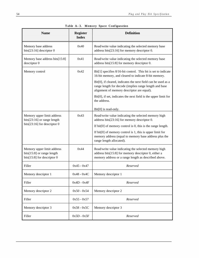
54 P lu g a n d P la y IS A S p e c if ic a t io n
Table ATable A--33. . Memory Space ConfigurationMemory Space Configuration
Name RegisterIndex
Definition
Memory base addressbits[23:16] descriptor 0
0x40 Read/write value indicating the selected memory baseaddress bits[23:16] for memory descriptor 0.
Memory base address bits[15:8]descriptor 0
0x41 Read/write value indicating the selected memory baseaddress bits[15:8] for memory descriptor 0.
Memory control 0x42 Bit[1] specifies 8/16-bit control. This bit is set to indicate16-bit memory, and cleared to indicate 8-bit memory.
Bit[0], if cleared, indicates the next field can be used as arange length for decode (implies range length and basealignment of memory descriptor are equal).
Bit[0], if set, indicates the next field is the upper limit forthe address.
Bit[0] is read-only.
Memory upper limit addressbits[23:16] or range lengthbits[23:16] for descriptor 0
0x43 Read/write value indicating the selected memory highaddress bits[23:16] for memory descriptor 0.
If bit[0] of memory control is 0, this is the range length.
If bit[0] of memory control is 1, this is upper limit formemory address (equal to memory base address plus therange length allocated).
Memory upper limit addressbits[15:8] or range lengthbits[15:8] for descriptor 0
0x44 Read/write value indicating the selected memory highaddress bits[15:8] for memory descriptor 0, either amemory address or a range length as described above.
Filler 0x45 - 0x47 Reserved
Memory descriptor 1 0x48 - 0x4C Memory descriptor 1
Filler 0x4D - 0x4F Reserved
Memory descriptor 2 0x50 - 0x54 Memory descriptor 2
Filler 0x55 - 0x57 Reserved
Memory descriptor 3 0x58 - 0x5C Memory descriptor 3
Filler 0x5D - 0x5F Reserved

P lu g a n d P la y IS A S p e c if ic a t io n 55
Table A Table A--44. 32-bit Memory Space Configuration. 32-bit Memory Space Configuration
Name RegisterIndex
Definition
32 Bit Memory base addressbits[31:24] descriptor 0
0x76 Read/write value indicating the selected memory baseaddress bits[31:24] for 32 bit memory descriptor 0.
32 Bit Memory base addressbits[23:16] descriptor 0
0x77 Read/write value indicating the selected memory baseaddress bits[23:16] for 32 bit memory descriptor 0.
32 Bit Memory base addressbits[15:8] descriptor 0
0x78 Read/write value indicating the selected memory baseaddress bits[15:8] for 32 bit memory descriptor 0.
32 Bit Memory base addressbits[7:0] descriptor 0
0x79 Read/write value indicating the selected memory baseaddress bits[7:0] for 32 bit memory descriptor 0.
32 Bit Memory Control 0x7A Bits[7:3] Reserved and must return 0 on reads
Bits[2:1] Memory control. These bits indicate 8/16/32bit memory as follows:
00 8-bit memory01 16-bit memory10 Reserved11 32-bit memory
If bit[0] of memory control is 0, this is the range length.
If bit[0] of memory control is 1, this is upper limit formemory address (equal to memory base address plus therange length allocated).
Bit[0] is read-only.
Memory upper limit addressbits[31:24] or range lengthbits[31:24] for descriptor 0
0x7B Read/write value indicating the selected memory highaddress bits[31:24] for memory descriptor 0.
If bit[0] of memory control is 0, this is the range length.
If bit[0] of memory control is 1, this is upper limit formemory address (equal to memory base address plus therange length allocated).
Memory upper limit addressbits[23:16] or range lengthbits[23:16] for descriptor 0
0x7C Read/write value indicating the selected memory highaddress bits[23:16] for memory descriptor 0, either amemory address or a range length as described above.
(continued on next page)

56 P lu g a n d P la y IS A S p e c if ic a t io n
Name RegisterIndex
Definition
Memory upper limit addressbits[15:8] or range lengthbits[15:8] for descriptor 0
0x7D Read/write value indicating the selected memory highaddress bits[15:8] for memory descriptor 0, either amemory address or a range length as described above.
Memory upper limit addressbits[7:0] or range lengthbits[7:0] for descriptor 0
0x7E Read/write value indicating the selected memory highaddress bits[7:0] for memory descriptor 0, either amemory address or a range length as described above.
Filler 0x7F Reserved
32 Bit Memory descriptor 1 0x80 - 0x88 32 Bit Memory descriptor 1
Filler 0x89 - 0x8F Reserved
32 Bit Memory descriptor 2 0x90 - 0x98 32 Bit Memory descriptor 2
Filler 0x99 - 0x9F Reserved
32 Bit Memory descriptor 3 0xA0 - 0xA8 32 Bit Memory descriptor 3
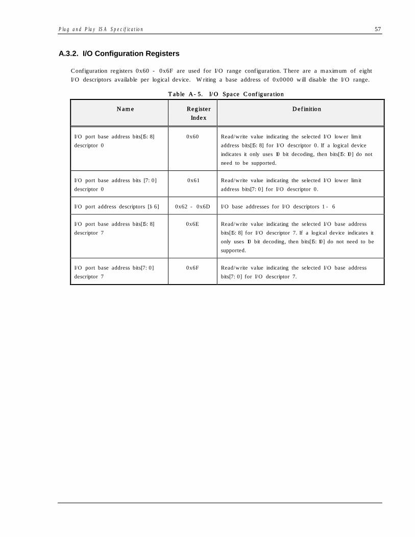
P lu g a n d P la y IS A S p e c if ic a t io n 57
A.3.2. I/O Configuration Registers
Configuration registers 0x60 - 0x6F are used for I/O range configuration. There are a maximum of eightI/O descriptors available per logical device. Writing a base address of 0x0000 will disable the I/O range.
Table ATable A--55. I/O Space Configuration. I/O Space Configuration
NameName RegisterRegisterIndexIndex
DefinitionDefinition
I/O port base address bits[15:8]
descriptor 0
0x60 Read/write value indicating the selected I/O lower limit
address bits[15:8] for I/O descriptor 0. If a logical device
indicates it only uses 10 bit decoding, then bits[15:10] do not
need to be supported.
I/O port base address bits [7:0]
descriptor 0
0x61 Read/write value indicating the selected I/O lower limit
address bits[7:0] for I/O descriptor 0.
I/O port address descriptors [1-6] 0x62 - 0x6D I/O base addresses for I/O descriptors 1 - 6
I/O port base address bits[15:8]
descriptor 7
0x6E Read/write value indicating the selected I/O base address
bits[15:8] for I/O descriptor 7. If a logical device indicates it
only uses 10 bit decoding, then bits[15:10] do not need to be
supported.
I/O port base address bits[7:0]
descriptor 7
0x6F Read/write value indicating the selected I/O base address
bits[7:0] for I/O descriptor 7.

58 P lu g a n d P la y IS A S p e c if ic a t io n
A.3.3. Interrupt Configuration Registers
Each logical device in a Plug and Play ISA card may use up to two interrupt requests and up to two DMAchannels. These can be selected by writing to the appropriate configuration register.
Table ATable A--66. Interrupt Configuration. Interrupt Configuration
NameName RegisterRegisterIndexIndex
DefinitionDefinition
Interrupt request level select 0 0x70 Read/write value indicating selected interrupt level.
Bits[3:0] select which interrupt level is used for Interrupt 0.
One selects IRQL 1, fifteen selects IRQL fifteen. IRQL 0
is not a valid interrupt selection and represents no interrupt
selection.
Interrupt request type select 0 0x71 Read/write value indicating which type of interrupt is used
for the Request Level selected above.
Bit[1] : Level, 1 = high, 0 = low
Bit[0] : Type, 1 = level, 0 = edge
If a card only supports 1 type of interrupt, this register
may be read-only.
Interrupt request level select 1 0x72 Read/write value indicating selected interrupt level.
Bits[3:0] select which interrupt level is used for Interrupt 0.
One selects IRQL 1, fifteen selects IRQL fifteen. IRQL 0
is not a valid interrupt selection and represents no interrupt
selection.
Interrupt request type select 1 0x73 Read/write value indicating which type of interrupt is used
for the Request Level selected above.
Bit[1] : Level, 1 = high, 0 = low
Bit[0] : Type, 1 = level, 0 = edge
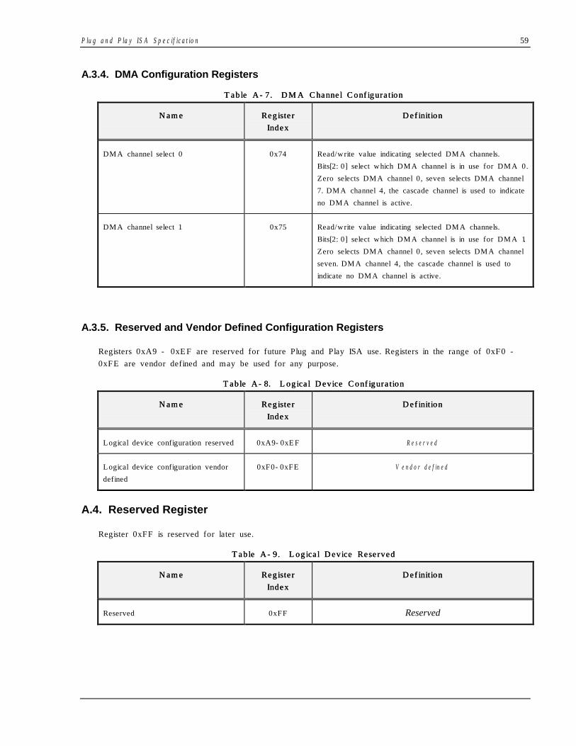
P lu g a n d P la y IS A S p e c if ic a t io n 59
A.3.4. DMA Configuration Registers
Table ATable A--77. DMA Channel Configuration. DMA Channel Configuration
NameName RegisterRegisterIndexIndex
DefinitionDefinition
DMA channel select 0 0x74 Read/write value indicating selected DMA channels.
Bits[2:0] select which DMA channel is in use for DMA 0.
Zero selects DMA channel 0, seven selects DMA channel
7. DMA channel 4, the cascade channel is used to indicate
no DMA channel is active.
DMA channel select 1 0x75 Read/write value indicating selected DMA channels.
Bits[2:0] select which DMA channel is in use for DMA 1.
Zero selects DMA channel 0, seven selects DMA channel
seven. DMA channel 4, the cascade channel is used to
indicate no DMA channel is active.
A.3.5. Reserved and Vendor Defined Configuration Registers
Registers 0xA9 - 0xEF are reserved for future Plug and Play ISA use. Registers in the range of 0xF0 -0xFE are vendor defined and may be used for any purpose.
Table ATable A--88. Logical Device Configuration. Logical Device Configuration
NameName RegisterRegisterIndexIndex
DefinitionDefinition
Logical device configuration reserved 0xA9-0xEF R e s e r v e d
Logical device configuration vendor
defined
0xF0-0xFE V e n d o r d e f in e d
A.4. Reserved Register
Register 0xFF is reserved for later use.
Table ATable A--99. Logical Device Reserved. Logical Device Reserved
NameName RegisterRegisterIndexIndex
DefinitionDefinition
Reserved 0xFF Reserved

60 P lu g a n d P la y IS A S p e c if ic a t io n
Appendix B. LFSR Definition
The Plug and Play ISA cards use a lin e a r f e e d b a c k s h if t r e g is t e r (LFSR) to generate data patterns needed toprovide an initiation key protocol and to provide a checksum verification during serial data read in theisolation protocol.
The LFSR is an 8-bit shift register that resets to the value 0x6A. The feedback taps for this shift registerare taken from register bits LFSR[0] and LFSR[1].
7 6 5 4 2 1 0
Write to address port
Shift out
Reset values 0 1 1 0 1 1 0
3
0init_key
Figure BFigure B--11 . Initiation Key LFSR. Initiation Key LFSR
B.1. Initiation LFSR Function
The initiation key is sent to the Plug and Play cards in the W a i t f o r K e yW a i t f o r K e y state by insuring that the LFSR isin its initial state, then performing 32 writes to the ADDRESS port. The 32 writes must be exactly equal tothe 32 values the LFSR will generate starting from 0x6A.
The LFSR will reset to its initial state (0x6A) any time the Plug and Play card is in the W a i t f o r K e y W a i t f o r K e y stateand receives a write to the ADDRESS port that does not match the value currently in the LFSR. To insurethat the LFSR is in the initial state, perform two write operations of value 0x00 to the ADDRESS portbefore sending the initiation key.
To perform the initiation key, first write the initial value of 0x6A to the ADDRESS port. Compute the next31 values of the LFSR by first determining the shift input for the next cycle which is LFSR[1] XOR LFSR[0].Next shift the LFSR right one bit and assign bit 7 to the shift input determined above. Write this value tothe ADDRESS port and repeat.
The exact sequence for the initiation key in hexadecimal notation is:
6A,B5,DA,ED,F6,FB,7D,BE,
DF,6F,37,1B,0D,86,C3,61
B0,58,2C,16,8B,45,A2,D1,
E8,74,3A,9D,CE,E7,73,39
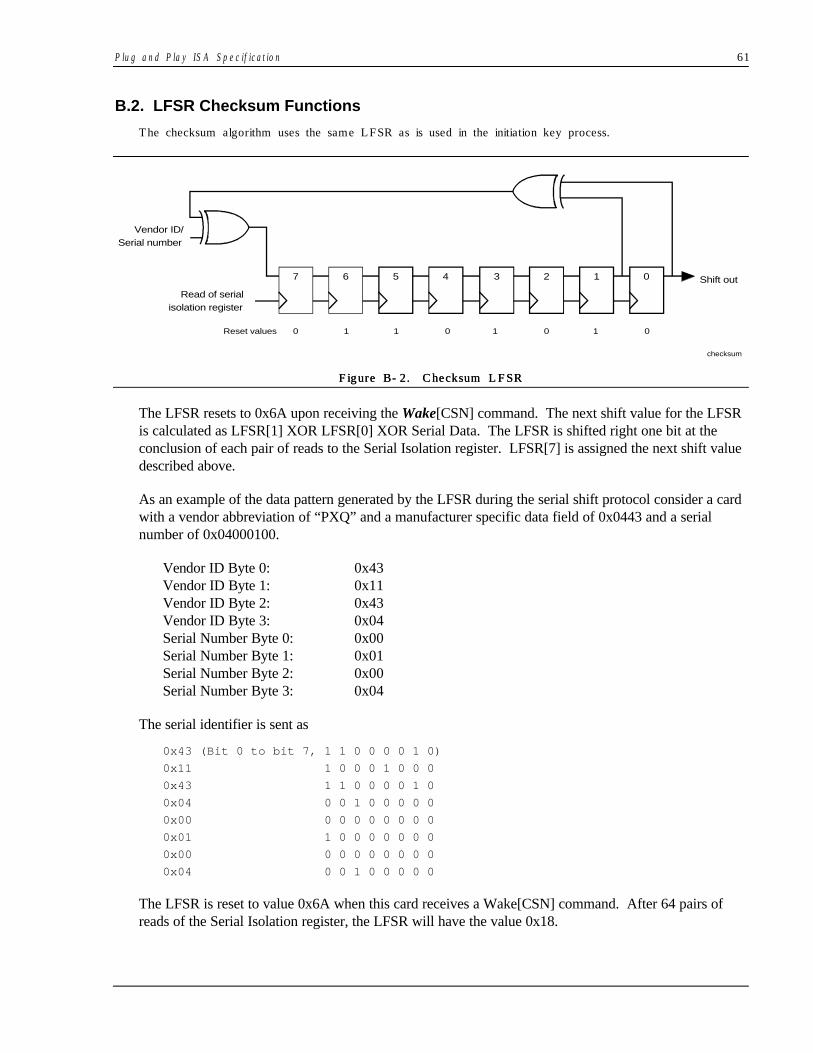
P lu g a n d P la y IS A S p e c if ic a t io n 61
B.2. LFSR Checksum Functions
The checksum algorithm uses the same LFSR as is used in the initiation key process.
7 6 5 4 2 1 0
Read of serial isolation register
Shift out
Reset values 0 1 1 0 1 1 0
3
0
Vendor ID/Serial number
checksum
Figure BFigure B--22. Checksum LFSR. Checksum LFSR
The LFSR resets to 0x6A upon receiving the Wake[CSN] command. The next shift value for the LFSRis calculated as LFSR[1] XOR LFSR[0] XOR Serial Data. The LFSR is shifted right one bit at theconclusion of each pair of reads to the Serial Isolation register. LFSR[7] is assigned the next shift valuedescribed above.
As an example of the data pattern generated by the LFSR during the serial shift protocol consider a cardwith a vendor abbreviation of “PXQ” and a manufacturer specific data field of 0x0443 and a serialnumber of 0x04000100.
Vendor ID Byte 0: 0x43Vendor ID Byte 1: 0x11Vendor ID Byte 2: 0x43Vendor ID Byte 3: 0x04Serial Number Byte 0: 0x00Serial Number Byte 1: 0x01Serial Number Byte 2: 0x00Serial Number Byte 3: 0x04
The serial identifier is sent as
0x43 (Bit 0 to bit 7, 1 1 0 0 0 0 1 0)
0x11 1 0 0 0 1 0 0 0
0x43 1 1 0 0 0 0 1 0
0x04 0 0 1 0 0 0 0 0
0x00 0 0 0 0 0 0 0 0
0x01 1 0 0 0 0 0 0 0
0x00 0 0 0 0 0 0 0 0
0x04 0 0 1 0 0 0 0 0
The LFSR is reset to value 0x6A when this card receives a Wake[CSN] command. After 64 pairs ofreads of the Serial Isolation register, the LFSR will have the value 0x18.

62 P lu g a n d P la y IS A S p e c if ic a t io n
Appendix C. Possible Enhancements
This appendix addresses several enhancements related to the configuration problem but not solved by thisproposal.
C.1. Plug and Play Boot Devices
The type of cards required before boot are: a display device, an input device, any device that hasexpansion ROM, and an initial program load device(s). Plug and Play ISA cards that are needed during theboot process must power up active. Plug and Play configuration may be implemented in system BIOS or inan operating system environment. In systems where Plug and Play configuration is implemented in the systemBIOS, the BIOS takes the responsibility of configuring all Plug and Play cards needed for booting the system.The default configuration may be over-ridden to have a conflict-free configuration. In systems where Plugand Play configuration does not take place until after an OS is loaded, Plug and Play devices required beforeboot should provide a secondary mechanism such as jumpers, switches or configuration EEPROM(preferred), that will allow a user to set a power-up configuration. This will provide the same functionalityavailable today for users to configure the ISA bus and boot their system. The method used to set theseconfiguration options is up to the card designer and beyond the scope of this document.
The default resource usage of a card is always reflected in the card's configuration registers. Thisinformation will allow the Plug and Play configuration or a driver to easily determine the default settings of aPlug and Play boot device regardless of the operating system the device driver was written for. Theresource use of the boot devices may be over-ridden by the operating system dependent Plug and Playconfiguration with full co-operation of the device driver. This functionality coupled with the fact that non-boot Plug and Play devices do not power up active will lower the amount of user intervention necessary toconfigure a system as well as increase the chance the system will boot.
Some devices will always be boot devices. For this class of device, except for disable, no user selectableoptions need to be included on the card to control booting.
There is another class of device, such as a network interface card, that may be a boot device in somesituations and not a boot device in others. For this type of device, a user selectable option should beincluded on the card that will allow the user to select the device to be active at boot time or not. Whetherthis is a switch, a jumper or an EEPROM setting and how this setting is selected is up to the card designerand beyond the scope of this document.

P lu g a n d P la y IS A S p e c if ic a t io n 63
C.2. BIOS Support for Plug and Play Devices
Refer to the P lu g a n d P la y B IO S S p e c if ic a t io n , v e r s io n 1.0 a for details on BIOS support for Plug and Play ISA
cards.
C.3. Plug and Play Devices and Non-Plug and Play Operating Systems
Plug and Play ISA devices may be used with non-Plug and Play operating systems by adding Plug and Playcode to the appropriate driver. For non-boot devices, the devices will remain inactive until their specificdriver is loaded. The driver will query all Plug and Play ISA cards in a system and find out which resourcesare in use. The driver will then configure the card to a location it believes to be conflict free and save thisconfiguration. In this way, all Plug and Play ISA cards are configured and operate in an environment that isbetter than the environment today.
For boot devices in operating system environments that do not support Plug and Play, configuration will relyon boot configuration done by the user as well as Plug and Play configuration performed by the devicedriver. Boot devices must be configured by either manually setting options or running a setup utility toconfigure the device.

64 P lu g a n d P la y IS A S p e c if ic a t io n
Appendix D. Sample Configuration Record for ABC EthernetCard
The ABC card does not require any DMA or memory resources. It requires one interrupt channel (anyIRQ) and requires a single I/O port in the 0x200 - 0x3E0 range (0x10 bytes aligned). The card doesn'thave any additional on-board information. The vendor ID of ABC is “ABC.” The vendor assigned partnumber for this card is 0x5090 and the serial # is 0x8C123456. The card has only one logical device, anEthernet controller. There are no compatible devices with this logical device. The following record should bereturned by the card during the identification phase:
;;;;;;;;;;;;;;;;;;;;;;;;;;;;;;;;;;;;;; Plug and Play Header;;;;;;;;;;;;;;;;;;;;;;;;;;;;;;;;;;;;;
DB 0x04 ; Vendor EISA ID Byte 0DB 0x43 ; Vendor EISA ID Byte 1DB 0x90 ; Vendor assigned product number (Byte 0)DB 0x50 ; Vendor assigned product number (Byte 1)DB 0x56 ; Serial Number Byte 0DB 0x34 ; Serial Number Byte 1DB 0x12 ; Serial Number Byte 2DB 0x8C ; Serial Number Byte 3DB Check Sum ; check sum calculated on above bits;;;;;;;;;;;;;;;;;;;;;;;;;;;;;;;;;;;;;; Plug and Play Version;;;;;;;;;;;;;;;;;;;;;;;;;;;;;;;;;;;;;DB 0x0A ; Small Item, Plug and Play versionDB 0x10 ; BCD major version [7:4] = 1
; BCD minor version [3:0] = 0DB 0x00 ; Vendor specified version number;;;;;;;;;;;;;;;;;;;;;;;;;;;;;;;;;;;;;; Identifier String (ANSI);;;;;;;;;;;;;;;;;;;;;;;;;;;;;;;;;;;;;DB 0x82 ; Large item, type identifier string(ANSI)DB 0x1C ; Length Byte 0 (28)DB 0x00 ; Length Byte 1DB "ABC Ethernet Network Adapter" ; Identifier string
;;;;;;;;;;;;;;;;;;;;;;;;;;;;;;;;;;;;;; Logical Device ID;;;;;;;;;;;;;;;;;;;;;;;;;;;;;;;;;;;;;
DB 0x15 ; Small item, type logical device IDDB 0x04 ; Vendor EISA ID Byte 0DB 0x43 ; Vendor EISA ID Byte 1DB 0x00 ; Vendor assigned function ID (Byte 0)DB 0x01 ; Vendor assigned function ID (Byte 1)DB 0x01 ; Logical device Flags[0]- required for boot
(Continued on next page)
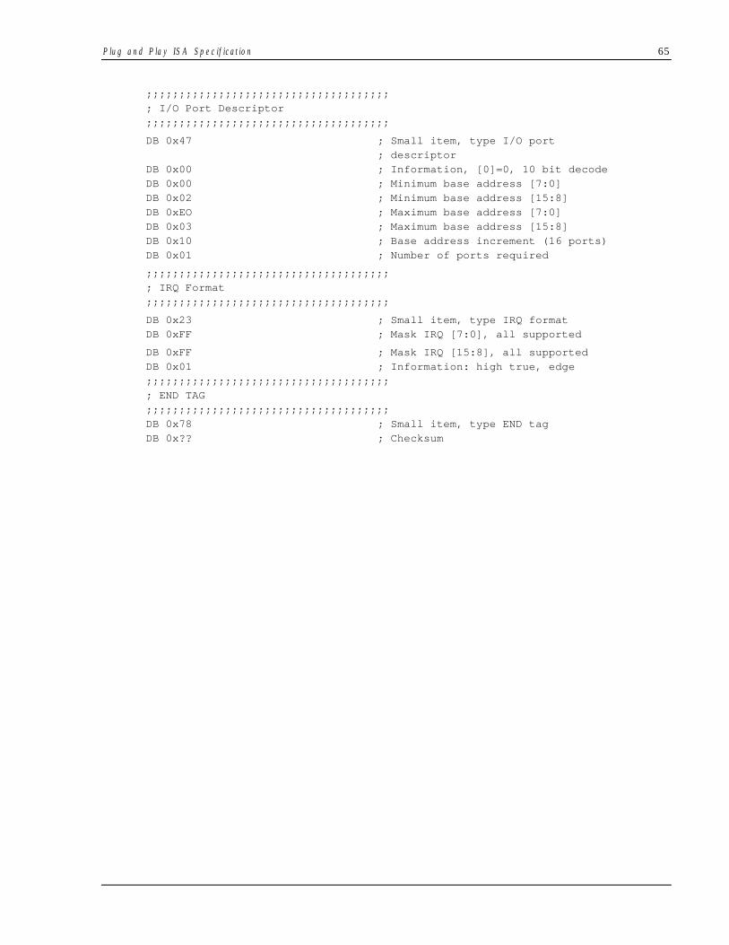
P lu g a n d P la y IS A S p e c if ic a t io n 65
;;;;;;;;;;;;;;;;;;;;;;;;;;;;;;;;;;;;;; I/O Port Descriptor;;;;;;;;;;;;;;;;;;;;;;;;;;;;;;;;;;;;;
DB 0x47 ; Small item, type I/O port; descriptor
DB 0x00 ; Information, [0]=0, 10 bit decodeDB 0x00 ; Minimum base address [7:0]DB 0x02 ; Minimum base address [15:8]DB 0xEO ; Maximum base address [7:0]DB 0x03 ; Maximum base address [15:8]DB 0x10 ; Base address increment (16 ports)DB 0x01 ; Number of ports required
;;;;;;;;;;;;;;;;;;;;;;;;;;;;;;;;;;;;;; IRQ Format;;;;;;;;;;;;;;;;;;;;;;;;;;;;;;;;;;;;;
DB 0x23 ; Small item, type IRQ formatDB 0xFF ; Mask IRQ [7:0], all supported
DB 0xFF ; Mask IRQ [15:8], all supportedDB 0x01 ; Information: high true, edge;;;;;;;;;;;;;;;;;;;;;;;;;;;;;;;;;;;;;; END TAG;;;;;;;;;;;;;;;;;;;;;;;;;;;;;;;;;;;;;DB 0x78 ; Small item, type END tagDB 0x?? ; Checksum