predicted electronic markers for polytypes of laobis 2
TRANSCRIPT

University of KentuckyUKnowledge
Physics and Astronomy Faculty Publications Physics and Astronomy
2-9-2017
Predicted Electronic Markers for Polytypes ofLaOBiS2 Examined via Angle-ResolvedPhotoemission SpectroscopyXiaoqing ZhouUniversity of Colorado - Boulder
Qihang LiuUniversity of Colorado - Boulder
J. A. WaughUniversity of Colorado - Boulder
T. NummyUniversity of Colorado - Boulder
Xiuwen ZhangUniversity of Colorado - Boulder
See next page for additional authors
Click here to let us know how access to this document benefits you.Follow this and additional works at: https://uknowledge.uky.edu/physastron_facpub
Part of the Condensed Matter Physics Commons
This Article is brought to you for free and open access by the Physics and Astronomy at UKnowledge. It has been accepted for inclusion in Physics andAstronomy Faculty Publications by an authorized administrator of UKnowledge. For more information, please contact [email protected].
Repository CitationZhou, Xiaoqing; Liu, Qihang; Waugh, J. A.; Nummy, T.; Zhang, Xiuwen; Zhu, Xiangde; Cao, Gang; Zunger, Alex; and Dessau, D. S.,"Predicted Electronic Markers for Polytypes of LaOBiS2 Examined via Angle-Resolved Photoemission Spectroscopy" (2017). Physicsand Astronomy Faculty Publications. 521.https://uknowledge.uky.edu/physastron_facpub/521

AuthorsXiaoqing Zhou, Qihang Liu, J. A. Waugh, T. Nummy, Xiuwen Zhang, Xiangde Zhu, Gang Cao, Alex Zunger,and D. S. Dessau
Predicted Electronic Markers for Polytypes of LaOBiS2 Examined via Angle-Resolved PhotoemissionSpectroscopy
Notes/Citation InformationPublished in Physical Review B, v. 95, issue 7, 075118, p. 1-9.
©2017 American Physical Society
The copyright holder has granted permission for posting the article here.
Digital Object Identifier (DOI)https://doi.org/10.1103/PhysRevB.95.075118
This article is available at UKnowledge: https://uknowledge.uky.edu/physastron_facpub/521

PHYSICAL REVIEW B 95, 075118 (2017)
Predicted electronic markers for polytypes of LaOBiS2 examined via angle-resolvedphotoemission spectroscopy
Xiaoqing Zhou,1 Qihang Liu,2,* J. A. Waugh,1 Haoxiang Li,1 T. Nummy,1 Xiuwen Zhang,2 Xiangde Zhu,3 Gang Cao,4
Alex Zunger,2,† and D. S. Dessau1,2,‡1Department of Physics, University of Colorado at Boulder, Boulder, Colorado 80309, USA
2Renewable and Sustainable Energy Institute, University of Colorado at Boulder, Boulder, Colorado 80309, USA3High Magnetic Field Laboratory of the Chinese Academy of Sciences, Hefei, China
4University of Kentucky, Lexington, Kentucky 40506, USA(Received 9 July 2016; revised manuscript received 10 November 2016; published 9 February 2017)
The natural periodic stacking of symmetry-inequivalent planes in layered compounds can lead to the formationof natural superlattices; albeit close in total energy, (thus in their thermodynamic stability), such polytypesuperlattices can exhibit different structural symmetries, thus have markedly different electronic properties whichcan in turn be used as “structural markers”. We illustrate this general principle on the layered LaOBiS2 compoundwhere density-functional theory (DFT) calculations on the (BiS2)/(LaO)/(BiS2) polytype superlattices revealboth qualitatively and quantitatively distinct electronic structure markers associated with the Rashba physics, yetthe total energies are only ∼ 0.1 meV apart. This opens the exciting possibility of identifying subtle structuralfeatures via electronic markers. We show that the pattern of removal of band degeneracies in different polytypes bythe different forms of symmetry breaking leads to Rashba “minigaps” with characteristic Rashba parameters thatcan be determined from spectroscopy, thereby narrowing down the physically possible polytypes. By identifyingthese distinct DFT-predicted fingerprints via angle-resolved photoemission spectroscopy (ARPES) measurementson LaBiOS2 we found the dominant polytype with small amounts of mixtures of other polytypes. This conclusion,consistent with neutron scattering results, establishes ARPES detection of theoretically established electronicmarkers as a powerful tool to delineate energetically quasidegenerate polytypes.
DOI: 10.1103/PhysRevB.95.075118
I. INTRODUCTION
Ordered crystalline compounds of fixed composition aregenerally assumed to have a unique and specific crystallo-graphic structure being distinctly separate from other phases inthe low-temperature phase diagram. An exception is polytypesthat represent an energetically closely spaced set of orderedcompounds, with the same composition often differing byorientations of certain subunits. The best known examples arezincblende and wurtzite polytypes of binary semiconductors[1], best exemplified by SiC that shows ∼100 polytypes [2],or ZnO, with ZnS appearing as either zincblende or wurtzite.What makes such polytypes electronically interesting is thatdespite a tiny difference in their thermodynamic stability(usually, the total energy difference is only on the order of lessthan 10 meV/atom [3]), their electronic properties can differsignificantly. For example, the difference in band gap of SiC4H and 3C polytypes is almost 1 eV [4], and the wurtzite formof III–V nitrides is polar, whereas 3C is nonpolar, a distinctionthat alters profoundly the electric field profile in nitride lasersand light-emitting diodes [5].
With the recent interest in the condensed matter physicscommunity of layered two-dimensional (2D) compounds suchas graphene [6], the transition metal dichalcogenides [7], andtopological insulators [8], the stacking sequences of theselayers is expected to be of importance, especially in cases
*[email protected]†[email protected]‡[email protected]
where the individual 2D layers exhibit structural distortions(such as inequivalent in-plane bonds), the stacking of whichalong the perpendicular direction creates natural superlattices.Because of the great similarity in their thermodynamic ener-gies, polytype physics is rather difficult to explore by conven-tional structural probes. Yet, various stacking sequences maymaintain or break inversion symmetry that can then play a rolein keeping or lifting certain degeneracies, with implicationsfor their electronic structure, spin polarization physics, andRashba physics. How to characterize and understand these“electronic markers” has only been minimally addressed,either theoretically or experimentally.
In this prototype system, we focus on the layered oxides ofthe type (BiS2)/(LaO)/(BiS2), where the 2D planes of BiS2 areseparated from each other by the LaO barrier [Fig. 1(a)]. Thismaterial has recently received a good deal of interest becauseof its potential to host unconventional superconductivity upto 10.6 K [9], hidden spin polarizations [10,11], spin fieldeffect transistors [12], electrically tunable Dirac cones [13],etc. In the previous studies, the compound was often assumedto have a centrosymmetric space group of P4/nmm and tohave a single specific crystallographic structure (called T0
here) [14–16]. However, such high-symmetry structure havingtwo equal in-plane Bi-S bonds reported in the InorganicCrystal Structure Database (ICSD) has been predicted byYildirim [17] to be dynamically unstable, and further neutrondiffraction experiments [18] confirmed that the two Bi-Sbonds have different lengths. Some of the present authors[19] examined via density functional theory (DFT) variouspolytype arrangements of the individual 2D planes havingunequal Bi-S bonds and predicted three stable classes of
2469-9950/2017/95(7)/075118(9) 075118-1 ©2017 American Physical Society

XIAOQING ZHOU et al. PHYSICAL REVIEW B 95, 075118 (2017)
FIG. 1. (a) The layered structure of LaOBiS2 with the unit cellindicated by the black frame. The green, red, purple, and yellow ballsrepresent La, O, Bi, and S atoms, respectively. Note that there are twoBiS2 layers in each unit cell. (b) Different stacking configurationsof two BiS2 layers for unstable structure T0 and its three stablepolytypes T1–T3. Compared with T0, the Bi-S1 2D networks ofT1–T3 have an in-plane distortion showing displacement of the S1atom along the x or y direction, and thus two different Bi-S1 bondlengths.
polytypes (noted as T1–T3), some being centrosymmetricand some breaking inversion symmetry [Fig. 1(b)]. Althoughsuperconductivity (but not polytypes) of n-type doped LaBiO2
attracts a lot of research interest [9], in this paper, we focuson the effect of polytypism in the undoped material withoutthe structural evolution [18] introduced by F-doping. Weshow that such polytypes give rise to distinctly differentsymmetry-related electronic properties, even though their totalenergies are quasidegenerate [6]. For example, whereas in theT0 structure there is a crossing of two doubly degenerate bands[so the crossing point is fourfold degenerate, see Fig. 2(a)]due to its relatively higher symmetry, in other polytypes,we predict two characteristic types of (partial) degeneracyremoval [Fig. 2(a)] at X and Y points of the rectangular-shapedBrillouin zone (BZ), leading to the formation of internal“minigaps” within the valence band or the conduction band.Additionally, the Rashba bands manifest minima at differentwave vectors for different polytypes. By considering theelectronic structure of different polytypes, we discover certainelectronic markers that are predicted to be sensitive to polytypestacking and the ensuing symmetry. Thus, measurements ofsuch markers can be used in conjunction with theory todetermine structure, thereby complementing information fromconventional structural probes (diffraction). Here we presentdetailed angle-resolved photoemission spectroscopy (ARPES)results of this system, aiming for identifying the possiblepolytype physics in this system. Notably, ARPES providesus with the detailed band structure to be compared withdensity functional theory (DFT) calculations based on differentpolytypes. Our paper establishes spectroscopic detection oftheoretically established electronic markers as a powerful toolto delineate energetically quasidegenerate polytypes.
FIG. 2. (a) Illustration of two types of band motifs (BM) classified by the degree of degeneracy (indicated by the number in parentheses)at the X (1/2, 0, 0) and Y (0, 1/2, 0) points. Type-I BM manifests the fourfold degenerate Dirac point, which breaks into a pair of twofolddegenerate points with a minigap � (horizontal arrows) as type-II BM. Off high-symmetry points X or Y, type-II BM can have twofolddegenerate bands (black) or single degenerate bands (red and blue) according to the presence of inversion symmetry. (b–e) Band structures ofT0–T3 polytypes show different BM types at X and Y point, which act as an electronic marker. Beyond the X or Y points in either direction ofthese plots is the M point. The BM types are summarized in (f).
075118-2
PREDICTED ELECTRONIC MARKERS FOR POLYTYPES OF . . . PHYSICAL REVIEW B 95, 075118 (2017)
II. METHODS
A. DFT calculations
The equilibrium crystal structure was obtained by DFT totalenergy minimization performed with an energy tolerance of10−4 eV, and all atomic positions were relaxed with a force tol-erance of 10−3 eV/A. The electronic structures were calculatedby using the projector-augmented wave (PAW) pseudopoten-tial [20] and the exchange and correlation of Perdew, Burke,and Ernzerhof (PBE) [21] as implemented in the Vienna abinitio Simulation Package (VASP) [22]. The plane wave energycutoff (reflecting basis set size) was set to 550 eV. Spin-orbitcoupling was included as a perturbation to the pseudopotentialthroughout the calculation. We note that the PBE functional didnot take the long-range van der Waals (VDW) interaction intoaccount and thus usually overestimates the interlayer space.However, the VDW correction underestimates the in-planelattice constant and thus causes the T0 structure to be theground state, which contradicts the theoretical prediction andexperiments. Since the accuracy of the in-plane lattice constantis more important to the investigation of polytype physics,we used the PBE functional for the basis of calculation andanalysis.
B. Sample growth
High-quality single crystals of LaBiOS2 were grown usingCsCl/KCL as flux. The charge was sealed in a quartztube, fired at 850 °C and then slowly cooled down to roomtemperature. The technique is similar to that described inRef. [23]. The size of the single crystals studied is on the orderof 2.0 × 2.0 × 0.3 mm3. The chemical composition of eachsingle crystal studied was determined using energy-dispersivex-ray (EDX) analysis (Hitachi/Oxford 3000). Each samplestudied is confirmed to be stoichiometrically consistent withLaBiOS2. EDX and x-ray diffraction results indicate that thequality of single crystals is uniform, and the crystal cleaveseasily with the very flat cleaved surface. Although in thepresent paper we did not perform structure determination, thestructural analysis of neutron diffraction data can be foundelsewhere [24].
C. Photoemission
ARPES measurements have been carried out at AdvancedLight Source (ALS) beamline 10.0.1 and 4.0.3, as well asSwiss Light Source (SLS) beamline 9L with combinations ofmultiple beam energies (30–120 eV, every 10 eV), samplegeometries (incoming light along high-symmetry lines �-X,�-Y, and �-M), beam spot sizes (down to 30 × 100 μm2
at ALS 4.0.3 and at SLS), and light polarizations (linearhorizontal, linear vertical, circular right, and circular left). Allthe data appear to be consistent with the polytype scenariowith different matrix element effects.
III. PREDICTED ELECTRONIC MARKERS OFDIFFERENT LaOBiS2 POLYTYPES
The basic layered crystal structure of LaOBiS2 is shownin Fig. 1(a) with a sandwiched structure containing two BiS2
layers and an intermediate LaO layer. The T0 structure hashigh symmetry (space group #129, P4/nmm) with the xy
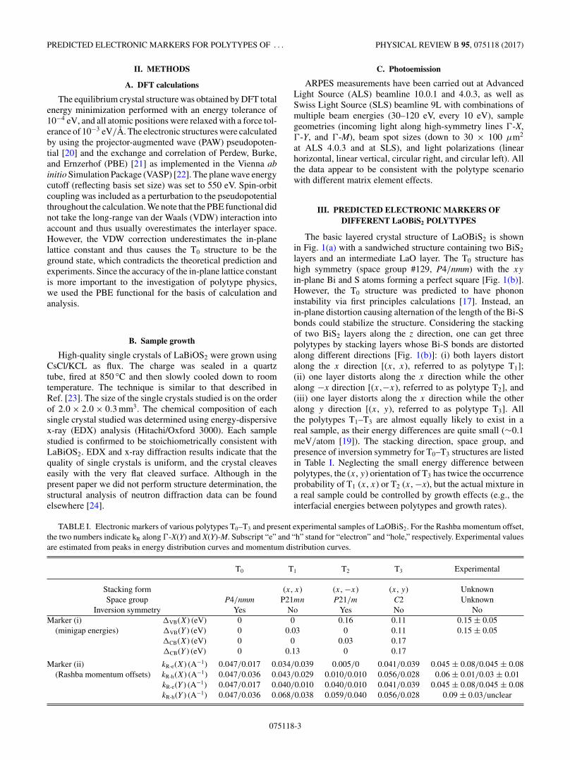
in-plane Bi and S atoms forming a perfect square [Fig. 1(b)].However, the T0 structure was predicted to have phononinstability via first principles calculations [17]. Instead, anin-plane distortion causing alternation of the length of the Bi-Sbonds could stabilize the structure. Considering the stackingof two BiS2 layers along the z direction, one can get threepolytypes by stacking layers whose Bi-S bonds are distortedalong different directions [Fig. 1(b)]: (i) both layers distortalong the x direction [(x, x), referred to as polytype T1];(ii) one layer distorts along the x direction while the otheralong −x direction [(x,−x), referred to as polytype T2], and(iii) one layer distorts along the x direction while the otheralong y direction [(x, y), referred to as polytype T3]. Allthe polytypes T1–T3 are almost equally likely to exist in areal sample, as their energy differences are quite small (∼0.1meV/atom [19]). The stacking direction, space group, andpresence of inversion symmetry for T0–T3 structures are listedin Table I. Neglecting the small energy difference betweenpolytypes, the (x, y) orientation of T3 has twice the occurrenceprobability of T1 (x, x) or T2 (x, −x), but the actual mixture ina real sample could be controlled by growth effects (e.g., theinterfacial energies between polytypes and growth rates).
TABLE I. Electronic markers of various polytypes T0–T3 and present experimental samples of LaOBiS2. For the Rashba momentum offset,the two numbers indicate kR along �-X(Y) and X(Y)-M. Subscript “e” and “h” stand for “electron” and “hole,” respectively. Experimental valuesare estimated from peaks in energy distribution curves and momentum distribution curves.
T0 T1 T2 T3 Experimental
Stacking form (x, x) (x, −x) (x, y) UnknownSpace group P4/nmm P21mn P21/m C2 Unknown
Inversion symmetry Yes No Yes No NoMarker (i) �VB(X) (eV) 0 0 0.16 0.11 0.15 ± 0.05
(minigap energies) �VB(Y ) (eV) 0 0.03 0 0.11 0.15 ± 0.05�CB(X) (eV) 0 0 0.03 0.17�CB(Y ) (eV) 0 0.13 0 0.17
Marker (ii) kR-e(X) (A−1) 0.047/0.017 0.034/0.039 0.005/0 0.041/0.039 0.045 ± 0.08/0.045 ± 0.08(Rashba momentum offsets) kR-h(X) (A−1) 0.047/0.036 0.043/0.029 0.010/0.010 0.056/0.028 0.06 ± 0.01/0.03 ± 0.01
kR-e(Y ) (A−1) 0.047/0.017 0.040/0.010 0.040/0.010 0.041/0.039 0.045 ± 0.08/0.045 ± 0.08kR-h(Y ) (A−1) 0.047/0.036 0.068/0.038 0.059/0.040 0.056/0.028 0.09 ± 0.03/unclear
075118-3

XIAOQING ZHOU et al. PHYSICAL REVIEW B 95, 075118 (2017)
We use DFT in the electronic structure calculation with thePAW pseudopotential [20] and the exchange and PBE corre-lation [21]. The equilibrium crystal structures are obtained byDFT total energy minimization (see Methods for more details).We note the following electronic markers of polytypism:
(i) Formation of polytype-dependent Rashba minigap atthe X or Y wave vectors in the BZ. Among the fourpolytypes considered here, T0 has the highest symmetry witha nonsymmorphic and centrosymmetric space group P4/nmm.Even though the combination of the two BiS2 layers in a unitcell creates a centrosymmetric structure, the system producesa Rashba-like splitting due to the locally noncentrosymmetricnature of each BiS2 sector, leading to two Rashba-like bandswith opposite helical spin topology [11]. The two bandcrossing points at wave vectors X(Y) are superimposed byscrew axis operation along the x(y) real space direction,leading to fourfold degeneracy (including spin). The effectiveHamiltonian around the wave vector X involves a 4 × 4 Diracmatrix, rendering a 3D Dirac cone (on a small energy scalenear the degeneracy point) that is robust even with spin-orbitcoupling (SOC) [25,26]. On the other hand, the bands off theX(Y) wave vectors are all twofold degenerate due to inversionsymmetry and time reversal symmetry. The result is twohorizontally shifted parabolas crossing at one point; we referto this type of band structure feature as “band motif I,” shownin Fig. 2(a). Each polytype has two band motifs—one at X andone at Y. DFT calculation verifies that in the T0 polytype, theband motif (BM) of both X and Y valleys are the same andbelong to type I, as shown in Fig. 2(b).
However, such Dirac points are not robust againstsymmetry-lowering perturbations. When the dynamically un-stable T0 evolves to its polytypes T1–T3, it looses nonsymmor-phic symmetries and thus removes the fourfold degeneracyof Dirac points at certain valleys, forming internal minigapswithin the valence and conduction bands. For T1 (space groupPmn21) structure, the remaining symmetry operation that canprotect the Dirac point is the screw axis {C2x |(1/2,0,0)},so it ensures Dirac cones at X, while due to the lossof {C2y |(1/2,0,0)} symmetry at the Y point, the fourfolddegeneracy splits into two Kramers pairs with a minigapbetween the split bands [see Fig. 2(c)]. Thus, the X point hasBM-I, whereas the Y point has BM-II. On the other hand, T2
(space group P 21/m) has {C2y |(1/2,0,0)} symmetry and thushosts Dirac points at Y and gapped states at X [see Fig. 2(d)].The BM having such a minigap at X(Y) instead of a Diracpoint is a “type II BM,” shown schematically in Fig. 2(a). Atype II BM could have twofold degenerate bands off X(Y) dueto inversion symmetry (as in T2), or singly degenerate bandsoff X(Y) due to the absence of inversion symmetry (as in T1).Finally, T3 has the lowest symmetry C2 without inversion, ornonsymmorphic symmetry, rendering identical gapped statesat both X and Y [see Fig. 2(e)].
Figure 2(f) summarizes the BM types of X and Y valleys forT0–T3 polytypes, showing that according to the classificationby the degree of degeneracy of the high-symmetry wavevectors, each of the four polytypes T0–T3 has a unique BM(X)and BM(Y). We further note that the polytype T1 that has areal space (y, y) stacking and T2 with a real space (x, −x)stacking each have one BM-I and one BM-II, so they areindistinguishable if one considers only the band motifs at the
individual X and Y wave vectors, but these polytypes would bedistinct if we add the marker minigap � for different bands andvalleys, illustrating distinct markers for different polytypes.For example, for T1, the minigap of conduction band (CB)�CB is larger than that of the valence band (VB) �VB, whilefor T2, the minigap �CB is smaller than that for �VB. For T3,the X and Y valleys are symmetric (see Table I).
(ii) The minima of the Rashba bands occur in differentwave vectors for different polytypes. The classical Rashbaspin splitting manifests two parabolic band dispersions shiftingtoward each other in momentum space. The band edges locatedoff the high-symmetry point are shown in Fig. 2(a). In BMtype I of centrosymmetric structures (T0 and T2), the bandsplitting along the �-X (�-Y) high-symmetry line that locatesinside the BZ is due to the combined contribution of thehybridization between two BiS2 layers and SOC, indicatinga larger momentum offset. In contrast, along X-M (Y-M)located at the surface of the BZ, the band splitting is purelySOC induced, while the layer hybridization is forbidden bythe nonsymmorphic symmetry. This effect is stronger forconduction bands in which the momentum offset along �-X isthree to four times larger than that along the X-M direction, asshown in Fig. 2. On the other hand, for the noncentrosymmetricpolytypes, especially T3, the anisotropy of momentum offsetalong different symmetry lines is strongly suppressed. Theband edges of both conduction band and valence band of thepolytypes are distinctly located at different wave vectors, asshown also in Table I. The dispersions of the conduction bandsand the valence bands, especially the band edges in momentumspace, could be a marker for identification by ARPES spectra.
IV. BAND STRUCTURE, DISPERSION AND FERMISURFACE—ELECTRONIC MARKERS FROM ARPES
Figure 3(a) shows the ARPES-measured Fermi map inthe first Brillouin zone, with four small electron pocketsfound at the X/Y points, which generally agree with thetheoretical predictions, as well as previous measurements[27,28] on F-doped compounds. Figure 3(b) shows an exampleof the zoomed-in spectra on one of the electron pockets, withdecreasing intensity in the second Brillouin zone. The Fermisurface around the X, Y points form two contour loops witha nearly square shape, indicating the Rashba band splitting.The band dispersions for the conduction bands and valencebands along the high-symmetry cut �-Y and X-M directionsare shown in Fig. 3(c).
From these we see that the band gap between the CB andVB is about 0.9 eV and that the sample is a lightly dopedn-type. This unintentional doping suggests the existence ofdonor defects (e.g., anion vacancies or donor antisite defects).Had they existed in high (e.g., percent) concentration, thismight contribute to spectral broadening. This unintentionaldoping is manifested by a shift of the Fermi energy above thatof the compensated material and allows a clear view of boththe conduction and valence bands with ARPES without thecomplication introduced by F-substituting.
We note that F substitution (indeed, alloying) is differentbecause it occurs at the ∼50% level, which has been shownto lack a symmetry breaking distortion in the Bi-S plane[17,18,29] and to modify charge fluctuations and phonon
075118-4

PREDICTED ELECTRONIC MARKERS FOR POLYTYPES OF . . . PHYSICAL REVIEW B 95, 075118 (2017)
-1.5
-1.0
-0.5
0.0
-0.9
-0.8
-0.7
-0.15
-0.15
0.15
0.15
-10
1
-1.0 0.0 1.0(a)
b(b)
Γ Y
ΜX
Γ Y/X M
(c)
FIG. 3. (a) Fermi map of lightly n-doped LaBiOS2 in the first Brillouin zone. Electron pockets are found near the X/Y points, the zoomed-inversion of which is shown in (b). ARPES spectra along high-symmetry cut �-Y/X-M (black arrows) are shown in (c) for conduction and valencebands. The data are raw and unsymmetrized, taken under 60 eV, circular-left polarized light coming along �-Y with 45° incidence angle inSwiss Light Source beamline 9L. Similar data on five other samples were obtained at the Swiss Light Source beamline 9L as well as at theAdvanced Light Source beamlines 4.0.3 and 10.0.1.
modes. The photoemission observed band splitting along �-Xis obvious, whereas the splitting along X-M is negligible[16,27]. According to the analysis of the present paper, the 50%alloyed compound of LiOFBiS2 is most likely a compound inits own right, with another kind of in-plane distortion and thusdifferent polytypes.
As shown in Fig. 3(c), there is a clear distinction betweenX/Y pockets, which implies the existence of T1/T2, as sucha distinction is a prediction of the polytype scenario for theT1/T2 cases. Nevertheless, there could still be a concern thatthe X and Y points shown here were not taken under identicalgeometrical conditions (i.e., with the same matrix elements).
To verify that the anisotropy between X/Y pockets is notrelated to the matrix element effect at all, we have repeatedthe experimental study by only rotating the sample azimuthangle by 90° and hence switching �-X to �-Y, as shown inFig. 4. (Note that this geometry is somewhat different fromthat used in Fig. 3.) Under such conditions, the matrix elementeffects must be the same between the two cuts in this figure, sothe clear differences between these cuts show the distinctionbetween the X and Y pockets, which has to arise from thepolytypism.
Examples of the zoomed-in spectra of the conductionbands and valence bands along the high symmetry direction
-1.5
-1.4
-1.3
-1.2
-1.1
-1.0
Γ Y MΓ X M-1.5
-1.4
-1.3
-1.2
-1.1
-1.0
Ener
gy (e
V)
(a) (b)
FIG. 4. ARPES spectra of the valence band near (a) the X pocket and (b) the Y pocket. Data were taken at ALS beamline 10.0.1 with 60 eV,linear horizontal polarized light coming in at a glancing angle along the �-X/�-Y direction, with the sample’s azimuth angle rotated by 90°from (a) to (b).
075118-5

XIAOQING ZHOU et al. PHYSICAL REVIEW B 95, 075118 (2017)
FIG. 5. Experimental spectra of (a) conduction bands along M-X-M direction; (b) conduction bands along �-Y-� direction, (c) valencebands along M-X-M direction, and (d) valence bands along �-Y-� direction, to be compared with DFT calculations of T0, T1, T2, and T3,respectively. ARPES spectra were taken under 60 eV, linear horizontal polarized light coming along the �-Y direction, with 45° incidence anglein Swiss Light Source beamline 9L. Similar data on five other samples were obtained at the Swiss Light Source beamline 9L as well as at theAdvanced Light Source beamlines 4.0.3 and 10.0.1.
M-X-M and Y-�-Y are presented in Fig. 5, to be comparedwith DFT predictions of T0, T1, T2, and T3, respectively. Afew observations are made in the following: (i) the typicallyassumed structure (single T0 polytype) is not able to explain thedata; (ii) the data support a superposition of polytypes, as nosingle polytype can explain all the data; and (iii) the dominantpolytype appears to be T3, as this captures the majority of themajor features, even though T1/T2 might also exist.
For the CB spectrum along M-X-M, the experimental data(Fig. 5, top left) shows a clear internal or central state thatis absent in the calculated spectrum for T0, as marked by thearrow in the second panel down, left column. This is a clearmarker that we need to go beyond the simplest structure (T0
polytype). The other polytypes, T1, T2, and T3, as calculatedfor this cut, all show the central state, though the differencesbetween the calculated structures for this cut are similarenough that we should look to other cuts to distinguish betweenthese possibilities.
On the other hand, the experimental conduction bandminima shown in top panels of Figs. 5(a) and 5(b) are at verymuch the same energy, which is at odds with the theoreticalprediction of a significant anisotropy of the CB minimum forboth the T1 and T2 polytypes, as highlighted in the lower panelsof Figs. 5(a) and 5(b). We note that the energy difference ofthe CB minima for polytypes T1 and T2 is a few hundredmillielectron volts different than for T0 and T3, even though
the overall system energy is about the same. Therefore, T1
and T2 can be ruled out as the lone or dominant polytypes,though a superposition of the two of these (minidomains) orthe addition of these with other polytypes could explain thelack of X/Y anisotropy of the CB minima.
Next, we consider more subtle but still clear effects in thedata, especially the Rashba minigaps, which are a deviationfrom the “classical” type of Rashba splitting that is well-knownfor many materials. This Rashba minigap is most clear inthe comparison of experimental data and DFT calculationsin Fig. 5(c), with it being more filled in or fully absentfor the other experimental cuts. To get a more quantitativecalibration, a direct comparison is shown in Fig. 6, with theleft panel showing the ARPES spectra and the right the DFTcalculations. In Fig. 6(a), it seems that the three polytypes T1,T2, and T3 can provide satisfying agreements; however, it isclear in Fig. 6(b) that the T3 polytype has to exist to matchthe experimental dispersions. Particularly, a direct comparisoncan be made between the band dispersions calculated in DFTand the experimental observation, even though there is someuncertainty due to the momentum broadening of the ARPESspectra. In Fig. 6(d), the ARPES spectra show a minigap thatseems to rule out a dominant T1 structure. On the other hand,in Fig. 6(e), the ARPES somewhat resembles a Dirac cone,suggesting a crossing. However, the intensity near the crossingpoint is suppressed, indicating that a minigap is still present.
075118-6

PREDICTED ELECTRONIC MARKERS FOR POLYTYPES OF . . . PHYSICAL REVIEW B 95, 075118 (2017)
-1.5
-1.4
-1.3
-1.2
-1.1
-1.0
M X M
M X M Γ Y Γ-0.3
-0.2
-0.1
0.0
0.1
Γ Y Γ-1.5
-1.4
-1.3
-1.2
-1.1
-1.0
-0.3
-0.2
-0.1
0.0
0.1
1
10
-1.5 -1.0
Γ-Y X-M
E-EF (eV)
(a) (b)
(e)(d)
(c)
FIG. 6. ARPES spectra (left panel) of (a) conduction bands along M-X-M cut; (b) conduction bands along �-Y-� cut; (d) valence bandsalong M-X-M cut, and (e) valence bands along �-Y-� cut, compared with DFT calculations (right panel) for T1 (red dash), T2 (blue dot), andT3 (black solid), respectively. (c) EDC at the X/Y point, the local maxima of which should correspond to the dominant bands while the localminimum suggests the existence of gapping. The size of the minigap can be estimated from the distance between the two peaks.
The existence of the minigap is better illustrated by the energydistribution curves (EDC) in Fig. 6(c). Although the spectralintensity here shows a highly unconventional exponentialenergy dependence, there are clearly two broad peaks witha dip in between, corresponding to a minigap, as predicted.The magnitude (∼0.015 eV) of the minigap can be estimatedfrom the separation of the broad peaks (arrows), while the
width of the peak introduces an uncertainty on the order of±0.005 eV. While there are still considerable intensities insidethe gap that might arise from strong impurity scattering, themagnitude of the gap is more consistent with the predictionsof DFT on the T2 and T3 structures.
ARPES spectra along the �-Y cut, as shown in Figs. 5(d)and 6(e), show a suppression of spectral weight in the regime
T1(a)
T2(e)
T3(i)
-0.3
-0.2
-0.1
0.0
0.1 (m)
T1(b)
T2(f)
T3(j)
-0.3
-0.2
-0.1
0.0
0.1 (n)
T1(c)
T2(g)
T3(k)
-1.5
-1.4
-1.3
-1.2
-1.1
-1.0 (o)
T1(d)
T2(h)
T3(l)
-1.5
-1.4
-1.3
-1.2
-1.1
-1.0 (p)
M X MM X M Γ Y ΓΓ Y Γ
FIG. 7. Simulations of ARPES spectra for the T1, T2, and T3 polytypes (top three rows, respectively) compared with ARPES data (bottomrow). Left two columns: CB spectra along M-X-M and along �-Y- �. Right two columns: VB spectra along M-X-M and �-Y- �. All spectra inthe bottom row were taken with 60-eV circular left polarized light coming along the �-Y direction at the Swiss Light Source beamline 9L.
075118-7
XIAOQING ZHOU et al. PHYSICAL REVIEW B 95, 075118 (2017)
of the minigap, but there are also some states there aswell. This would seem to favor a superposition of T3 withany of T0, T1, or T2, all of which have the presence of“central states.” The experimental momentum offsets [marker(ii)] are also tabulated in Table I and are most consistentwit the T3 structure as the dominant polytype. To furtherinvestigate the possible mixing of different polytypes, inFig. 7 we simulated the ARPES spectra from the DFTcalculations with the Green’s function and introduced constantenergy and momentum broadenings to mimic the quasiparticlescattering and instrumental resolution functions appropriatefor our experimental setup. We have also incorporated anexponential energy dependence to the valence band intensitiesto approximately match the experimental observations. It canbe seen that while T3 simulation agrees best with experimentalobservation, a superposition of all three possibilities mightmatch the data even better. However, it remains a challengeto fully account for all possible matrix element effects, whichmight have complex momentum and energy dependencies.
In summary, the data as a whole indicates that the T3
structure contributes most significantly to the ARPES signal,with an additional T1 and T2 mixing as a secondary effect. Thisis in part a consequence of the geometric factor (our predictionthat T3 has double the occurrence possibility as T1/T2) aswell as growth kinetics factors. A similar conclusion has beenrecently reached from the latest x-ray and neutron scatteringresults using very different but complementary metrics [24].
V. DISCUSSION AND CONCLUSION
Here we present a theory-guided approach to identifypolytypes with subtle structural deviations (that are hard toidentify with normal structural determination) via electronicmarkers, i.e., distinguishable electronic properties because ofthe different structural or spin-orbit features, especially includ-ing crystal symmetries. The effect of the symmetry changingpresented onto the electronic properties could be enhancedby other material-dependent factors. The most predominate
marker in our paper, the minigap in conduction and valencebands, is most strongly connected to the presence/breakingof nonsymmorphic screw axis symmetry at different wavevectors, with a smaller impact from SOC. This effect isanalogous to the Peierls distortion, which drives a metallicsystem to be semiconducting by opening a gap because ofthe structural dimerization. Therefore, such an approach is notlimited to the materials with large SOC, since the driving forceof such a marker is the change in structure and symmetry.
In this paper we demonstrate the capability of ARPES todistinguish subtle electronic markers of different polytypes inthe layered compound LaOBiS2. We found that the ARPESspectra are mostly consistent with the system being largely theT3 polytype, the knowledge of which might be crucial to ourunderstanding of the novel properties in this system. Whilethis paper focused on a specific material, it demonstrated thatdifferent polytypes or a mixture of those can be generallyidentified by their relevant electronic markers with ARPEStechniques. In the future, optical or transport experiments suchas interband absorption and emission may also be utilized toobserve or take advantage of such features, especially if theFermi energy could be tuned to the middle of some of theseRashba minigaps.
ACKNOWLEDGMENTS
This paper was funded by National Science Foundation(NSF) Designing Materials to Revolutionize and Engineer ourFuture (DMREF) Project No. DMR-1334170 to the Universityof Colorado and the University of Kentucky. We thank Feng Yefor help with some of the early structural characterizations ofthese materials. We thank Dr. S. K. Mo, Dr. Y. D. Chuang, Dr.J. D. Denlinger, Dr. N. C. Plumb, and Dr. M. Shi for technicalassistance on the ARPES measurements. The Advanced LightSource is supported by the Director, Office of Science, Officeof Basic Energy Sciences, of the U.S. Department of Energyunder Contract No. DE-AC02-05CH11231.
[1] C.-Y. Yeh, S.-H. Wei, and A. Zunger, Phys. Rev. B 50, 2715(1994).
[2] C. Cheng, R. J. Needs, and V. Heine, J. Phys. C 21, 1049(1988).
[3] C.-Y. Yeh, Z. W. Lu, S. Froyen, and A. Zunger, Phys. Rev. B 46,10086 (1992).
[4] L. Patrick, D. R. Hamilton, and W. J. Choyke, Phys. Rev. 143,526 (1966).
[5] S. Nakamura, Rev. Mod. Phys. 87, 1139 (2015).[6] A. K. Geim and K. S. Novoselov, Nat. Mater. 6, 183
(2007).[7] B. Radisavljevic, A. Radenovic, J. Brivio, V. Giacometti, and A.
Kis, Nat. Nanotechnol. 6, 147 (2011).[8] M. Z. Hasan and C. L. Kane, Rev. Mod. Phys. 82, 3045
(2010).[9] Y. Mizuguchi, S. Demura, K. Deguchi, Y. Takano, H. Fujihisa,
Y. Gotoh, H. Izawa, and O. Miura, J. Phys. Soc. Jpn. 81, 114725(2012).
[10] X. Zhang, Q. Liu, J.-W. Luo, A. J. Freeman, and A. Zunger, Nat.Phys. 10, 387 (2014).
[11] Q. Liu, X. Zhang, H. Jin, K. Lam, J. Im, A. J. Freeman, and A.Zunger, Phys. Rev. B 91, 235204 (2015).
[12] Q. Liu, Y. Guo, and A. J. Freeman, Nano Lett. 13, 5264(2013).
[13] X.-Y. Dong, J.-F. Wang, R.-X. Zhang, W.-H. Duan, B.-F.Zhu, J. O. Sofo, and C.-X. Liu, Nat. Commun. 6, 8517(2015).
[14] V. S. Tanryverdiev, O. M. Aliev, and I. I. Aliev, Inorg. Mater.31, 1497 (1995).
[15] J. Lee, M. B. Stone, A. Huq, T. Yildirim, G. Ehlers, Y.Mizuguchi, O. Miura, Y. Takano, K. Deguchi, S. Demura, andS.-H. Lee, Phys. Rev. B 87, 205134 (2013).
[16] L. K. Zeng, X. B. Wang, J. Ma, P. Richard, S. M. Nie, H. M.Weng, N. L. Wang, Z. Wang, T. Qian, and H. Ding, Phys. Rev.B 90, 054512 (2014).
[17] T. Yildirim, Phys. Rev. B 87, 020506 (2013).
075118-8
PREDICTED ELECTRONIC MARKERS FOR POLYTYPES OF . . . PHYSICAL REVIEW B 95, 075118 (2017)
[18] A. Athauda, J. Yang, S. Lee, Y. Mizuguchi, K. Deguchi, Y.Takano, O. Miura, and D. Louca, Phys. Rev. B 91, 144112(2015).
[19] Q. Liu, X. Zhang, and A. Zunger, Phys. Rev. B 93, 174119(2016).
[20] G. Kresse and D. Joubert, Phys. Rev. B 59, 1758 (1999).[21] J. P. Perdew, K. Burke, and M. Ernzerhof, Phys. Rev. Lett. 77,
3865 (1996).[22] G. Kresse and J. Furthmuller, Comput. Mater. Sci. 6, 15
(1996).[23] M. Nagao, A. Miura, S. Demura, K. Deguchi, S. Watauchi,
T. Takei, Y. Takano, N. Kumada, and I. Tanaka, Solid StateCommun. 178, 33 (2014).
[24] A. Athauda, C. Hoffman, Y. Ren, S. Aswartham, J. Terzic, G.Cao, X. Zhu, and D. Louca. arXiv:1601.07517.
[25] S. M. Young, S. Zaheer, J. C. Y. Teo, C. L. Kane, E. J. Mele,and A. M. Rappe, Phys. Rev. Lett. 108, 140405 (2012).
[26] L. M. Schoop, M. N. Ali, C. Straszer, A. Topp, A. Varykhalov,D. Marchenko, V. Duppel, S. S. P. Parkin, B. V. Lotsch, andC. R. Ast, Nat. Commun. 7, 11696 (2016).
[27] Z. R. Ye, H. F. Yang, D. W. Shen, J. Jiang, X. H. Niu, D. L.Feng, Y. P. Du, X. G. Wan, J. Z. Liu, X. Y. Zhu, H. H. Wen, andM. H. Jiang, Phys. Rev. B 90, 045116 (2014).
[28] K. Terashima, T. Wakita, M. Sunagawa, H. Fujiwara, T.Nagayama, K. Ono, H. Kumigashira, M. Nagao, S. Watauchi,I. Tanaka, H. Okazaki, Y. Takano, Y. Mizuguchi, H. Usui, K.Kuroki, Y. Muraoka, and T. Yokoya, J. Phys. Conf. Ser. 683,012002 (2016).
[29] A. Athauda, J. Yang, B. Li, Y. Mizuguchi, S. Lee, and D. Louca,J. Supercond. Novel Magn. 28, 1255 (2015).
075118-9