presentation - design, measurement and modeling of … measurement and modeling of ltcc embedded...
TRANSCRIPT

Design, Measurement and Modeling of LTCC Embedded Inductors and PCB
Balanced Devices
Prof. T.S. Horng (? ? ? )E.E. Dept., National Sun Yat-Sen Univ.Email: [email protected]

Outline
LTCC Embedded Inductors
PCB Balanced Devices
Conclusions

Design Trend
Planar Spiral Stacked Spiral Helical
≥ 222No. of Layers
HighestHigherLowQ(under the same Leff)
HighestHigherLowSRF(under the same Leff)
SmallestSmallerLargeArea(under the same Leff)
HelicalStacked SpiralPlanar SpiralLTCC Inductor

Measurement Techniques
Vector Network Analyzer
Test fixture
LTCCDevice
Reference plane after TRL calibration Electrode
Microstripline
LTCC Device(top view)
SG/GS-type probes
Test Fixture Microwave Probes

Test-Fixture Measurement vs. HFSS Simulation
Spiral inductor
The whole LTCC device
LTCC device on test fixture
Leff ≈ 6 nH
0 1 2 3 4 5 6 7 8 9 10
Frequency (GHz)
-50
-40
-30
-20
-10
0
dB
(S21
)
Mea#1Mea#2Mea#3Sim
0 1 2 3 4 5 6 7 8 9 10
Frequency (GHz)
-50
-40
-30
-20
-10
0
dB
(S11
)
Mea#1 Mea#2Mea#3Sim
Electrode
Microstrip line

Microwave-Probe Measurement vs. HFSS Simulation
Leff ≈ 6 nH
üSmaller areaüHigher SRFüHigher Q factorüBetter measured data repeatabilityüBetter agreement between simulation
and measurement
GS probe
0 1 2 3 4 5 6 7 8 9 10
Frequency (GHz)
-50
-40
-30
-20
-10
0
dB
(S21
)Mea#1Mea#2Sim
0 1 2 3 4 5 6 7 8 9 10
Frequency (GHz)
-50
-40
-30
-20
-10
0
dB
(S11
)
Mea#1 Mea#2Sim

A New Modified-T Model for Lossless Transmission Line
Lossless transmission lineZ0: Characteristic impedance
τ: Propagation delay
θ: Electrical length
pC
mL
sL sLsC
τ ,0Zθ
qωωπθ →=⇔→= 00
Equivalent π model
Equivalent Τ model
Equivalent modified-Τ model
≈?
ØIs it possible to create an equi-valent single-stage lumped model for a lossless transmission line having electrical length up to π ?
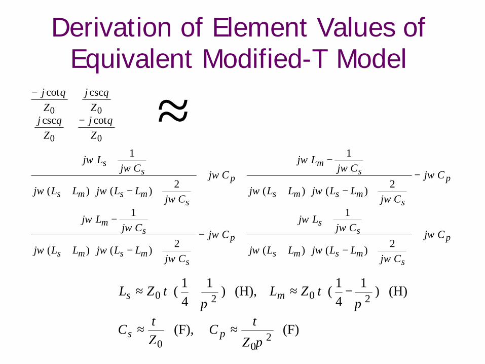
Derivation of Element Values of Equivalent Modified-T Model
+
+−+
+−
+−+
−
−
+−+
−+
+−+
+
−
−
p
smsms
ss
p
smsms
sm
p
smsms
sm
p
smsms
ss
Cj
CjLLjLLj
CjLj
Cj
CjLLjLLj
CjLj
Cj
CjLLjLLj
CjLj
Cj
CjLLjLLj
CjLj
Zj
Zj
Zj
Zj
2
)( )(
1
2
)( )(
1
2
)( )(
1
2
)( )(
1
cotcsc
csccot
00
00
ω
ωωω
ωω
ω
ωωω
ωω
ω
ωωω
ωω
ω
ωωω
ωω
θθ
θθ ≈
⇒ (F) (F),
(H) ) 1
41
( (H), ) 1
41
(
200
2020
π
ττπ
τπ
τ
ZC
ZC
ZLZL
ps
ms
≈≈
−≈+≈

Comparison of Bandwidth among Equivalent Models
π model
0 2 4 6 8 10 12 14 16
Freq(GHz)
-100
-90
-80
-70
-60
-50
-40
-30
-20
-10
0
S11
(dB
)
Lossless_TLModified-T_model
0 2 4 6 8 10 12 14 16
Freq(GHz)
-100
-90
-80
-70
-60
-50
-40
-30
-20
-10
0
S11
(dB
)
Lossless_TLPi_model
0 2 4 6 8 10 12 14 16
Freq(GHz)
-100
-90
-80
-70
-60
-50
-40
-30
-20
-10
0S11
(dB)
Lossless_TLT_model
T model
Modified-T model
θ = π θ = 2π θ = 3π
Transmission-line circuit
S11
(dB
)
S11
(dB
)
S11
(dB
)
ps 100 , 1000 =Ω= τZΩ 50 Ω 50

Comparison of Bandwidth among Equivalent Models
0 2 4 6 8 10 12 14 16
Freq(GHz)
-200
-150
-100
-50
0
50
100
150
200
S11
(phas
e)
Lossless_TLPi_model
0 2 4 6 8 10 12 14 16
Freq(GHz)
-200
-150
-100
-50
0
50
100
150
200
S11
(phas
e)Lossless_TLT_model
0 2 4 6 8 10 12 14 16
Freq(GHz)
-200
-150
-100
-50
0
50
100
150
200
S11
(ph
ase)
Lossless_TLModified-T_model
π modelModified-T model
T modelθ = π θ = 2π θ = 3π
Transmission-line circuitS
11 (p
has
e)
S11
(ph
ase)
S11
(ph
ase)
ps 100 , 1000 =Ω= τZΩ 50 Ω 50

Comparison of Bandwidth among Equivalent Models
0 2 4 6 8 10 12 14 16
Freq(GHz)
-20
-18
-16
-14
-12
-10
-8
-6
-4
-2
0
S21
(dB
)
Lossless_TLModified-T_model
0 2 4 6 8 10 12 14 16
Freq(GHz)
-20
-18
-16
-14
-12
-10
-8
-6
-4
-2
0
S21
(dB
)
Lossless_TLPi_model
0 2 4 6 8 10 12 14 16
Freq(GHz)
-20
-18
-16
-14
-12
-10
-8
-6
-4
-2
0
S21
(dB
)
Lossless_TLT_model
π modelModified-T model
T model
S21
(dB
)S
21 (d
B)
S21
(dB
)
θ = π θ = 2π θ = 3π
Transmission-line circuit
ps 100 , 1000 =Ω= τZΩ 50 Ω 50

Comparison of Bandwidth among Equivalent Models
0 2 4 6 8 10 12 14 16
Freq(GHz)
-200
-150
-100
-50
0
50
100
150
200
S21
(ph
ase)
Lossless_TLModified-T_model
0 2 4 6 8 10 12 14 16
Freq(GHz)
-200
-150
-100
-50
0
50
100
150
200
S21
(phas
e)
Lossless_TLPi_model
0 2 4 6 8 10 12 14 16
Freq(GHz)
-200
-150
-100
-50
0
50
100
150
200
S21
(phas
e)
Lossless_TLT_model
π modelModified-T model
T modelθ = π θ = 2π θ = 3π
Transmission-line circuitS
21 (p
has
e)S
21 (p
has
e)
S21
(ph
ase)
ps 100 , 1000 =Ω= τZΩ 50 Ω 50

Distributed Modified-T Model
τ ,0Z
πθ 3=
3/pC
3/mL
3/sL 3/sL3/sC
3/pC
3/mL
3/sL 3/sL3/sC
3/pC
3/mL
3/sL 3/sL3/sC
≈
3-stage modified-T model3π-long transmission line
0 2 4 6 8 10 12 14Frequency (GHz)
-180
-120
-60
0
60
120
Ph
ase(
S11
)
Lossless_TL 3-stage modified-T_model
0 2 4 6 8 10 12 14Frequency (GHz)
-3
-2.5
-2
-1.5
-1
-0.5
0
dB
(S21
)
Lossless_TL 3-stage modified-T_model
0 2 4 6 8 10 12 14Frequency (GHz)
-300
-180
-60
60
180P
has
e(S
21)
Lossless_TL 3-stage modified-T_model
0 2 4 6 8 10 12 14Frequency (GHz)
-60
-50
-40
-30
-20
-10
0
dB
(S11
)
Lossless_TL 3-stage modified-T_model
θ = π θ = 2π θ = 3π

Modified-T Models for Spiral Inductors
Leff ≈ 6 nH
pC
mL
sL sLsC
pL
1pC 1pL
pR
gCgL0 2 4 6 8 10 12 14
Frequency (GHz)
-35
-30
-25
-20
-15
-10
-5
0
dB
(S21
)
zero
1st by-pass 2nd by-pass
Ground Resonance
Shunt Cap
loss
Modified-T model sCsC effLsR
pCConventional π model

Comparison of Bandwidth between Two Inductor Models
0 2 4 6 8 10 12 14 16
Freq(GHz)
-45
-40
-35
-30
-25
-20
-15
-10
-5
0
S22
(dB
)
measurementmodeling
0 2 4 6 8 10 12 14 16
Freq(GHz)
-200
-150
-100
-50
0
50
100
150
200
S22
(ph
ase)
measurementmodeling
0 2 4 6 8 10 12 14 16
Freq(GHz)
-35
-30
-25
-20
-15
-10
-5
0
S11
(dB
)
measurementpi_model
0 2 4 6 8 10 12 14 16
Freq(GHz)
-200
-150
-100
-50
0
50
100
150
200
S11
(ph
ase)
measurementpi_modelmeasurementPi_model
measurementPi_model
measurementModified-T_model
measurementModified-T_model
S11
(dB
)
S11
(dB
)
S11
(ph
ase)
S11
(ph
ase)
Conventional π modelModified-T model

Comparison of Bandwidth between Two Inductor Models
0 2 4 6 8 10 12 14 16
Freq(GHz)
-30
-25
-20
-15
-10
-5
0
S21
(dB
)
measurementmodeling
0 2 4 6 8 10 12 14 16
Freq(GHz)
-150
-100
-50
0
50
100
150
200
S21
(ph
ase)
measurementmodeling
0 2 4 6 8 10 12 14 16
Freq(GHz)
-30
-25
-20
-15
-10
-5
0
S21
(dB
)
measurementpi_model
0 2 4 6 8 10 12 14 16
Freq(GHz)
-200
-150
-100
-50
0
50
100
150
200
S21
(ph
ase)
measurementpi_model
measurementPi_model
measurementPi_model
measurementModified-T_model
measurementModified-T_model
S21
(dB
)
S21
(dB
)
S21
(ph
ase)
S21
(ph
ase)
Conventional π modelModified-T model

Outline
LTCC Embedded Inductors
PCB Balanced Devices
Conclusions

Measurement Systems for Multiportand Mixed-Mode S-Parameters
ØPure Mode Network AnalyzerØMultiport Network Analyzer Using
Full-N Port CalibrationØTwo-Port Network Analyzer Using
Renormalization Techniques

Port Termination Problem
DUT
Port 3 terminated
1a
1b
2a
2b
3a 3b
Port 1 Port 2
Port 3
3332321313
3232221212
3132121111
aSaSaSb
aSaSaSb
aSaSaSb
++=++=
++=
Three-port Network Three-port S parameters
Reflection due to port termination
3
33 b
a=Γ
Measured two-port S parameters
Γ−Γ
+Γ−Γ
+
Γ−Γ
+Γ−Γ
+=
=
333
3322322
333
3312321
333
3321312
333
3311311
p3t22
p3t21
p3t12
p3t11p3t
11
11
][
SSS
SSSS
S
SSS
SSSS
S
SS
SSS

Partial Renormalization
[ ] [ ] [ ]( ) [ ] [ ]( ) [ ] [ ][ ]( ) [ ] [ ]( )
2,1for , where
00
00
11
=+−
=
−Γ−Γ−−=′ −−
kZZ
G
SUSUSSUS
kk
kkk ζ
ζ
DUT
Port 3 terminated
1a
1b
2a
2b
3a 3b
Port 1 Port 2
Port 3
1oZ 2oZ
3oZ
DUT
Port 3 terminated
1a
1b
2a
2b
3a 3b
Port 1 Port 2
Port 3
1oζ 2oζ
3oζ
⇒][S ][ 'S

Renormalization Transforms
=
=
= p1t
33p1t32
p1t23
p1t22p1t
p2t33
p2t31
p2t13
p2t11p2t
p3t22
p3t21
p3t12
p3t11p3t ][ , ][ , ][
SS
SSS
SS
SSS
SS
SSS
ØThree partial 2-port S-parameter measurements
ØAfter partial renormalizations
=
=
= m3
33m332
m323
m322m3
m233
m231
m213
m211m2
m122
m121
m112
m111m1 ][ , ][ , ][
SS
SSS
SSSSS
SSSSS
[ ] [ ] m233
m332
m231
m323
m122
m121
m213
m112
m111
S
SSS
SSSSSS
S ⇒
=′
ØConstruct the S matrix of the three-port network normalized to [ζ0] and then transform it back to the S matrix normalized to [Z0] :
renormalized to

Determination of [ζ0]
Ø Use TRL Calibration
Øi
ii Z
Γ−Γ+
=11
00ζ

DC-Block Branch-Line Coupler
000 2ZZZ ao
ae =−
000 2ZZZ ao
ae =−
Port 1 Port 2
Port 4 Port 3
Design guide Photo of component

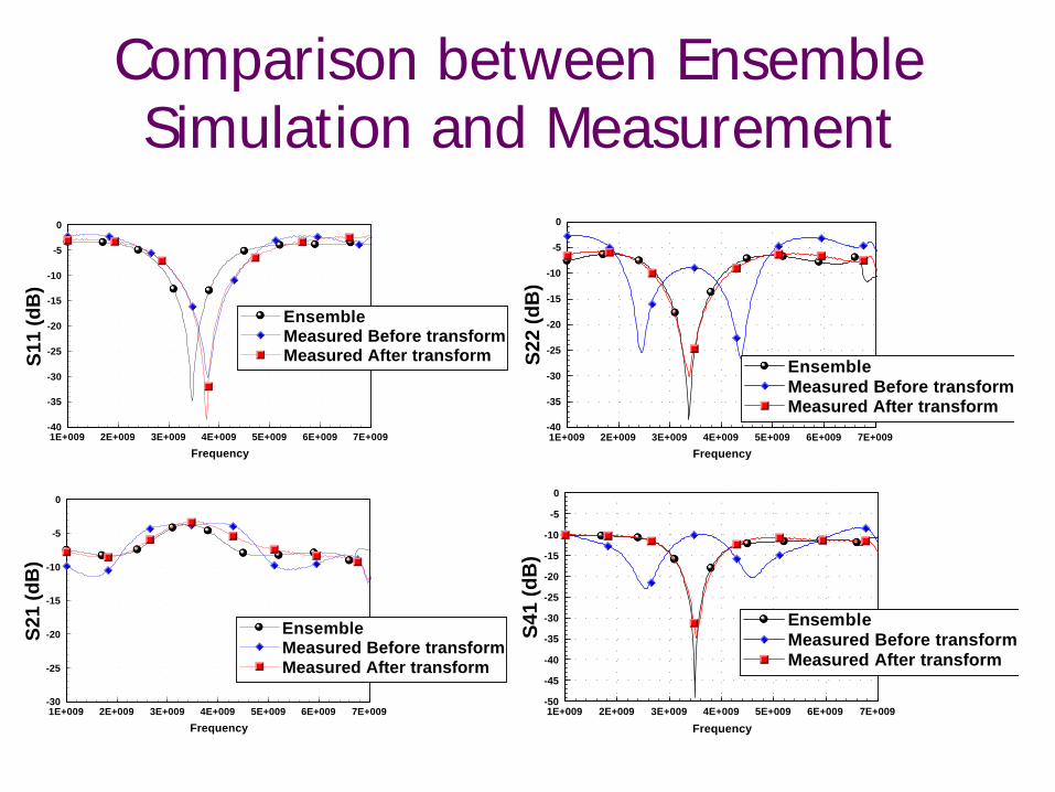
Comparison between Ensemble Simulation and Measurement
1E+009 2E+009 3E+009 4E+009 5E+009 6E+009 7E+009
Frequency
-30
-25
-20
-15
-10
-5
0
S11
(d
B)
EnsembleMeasured
1E+009 2E+009 3E+009 4E+009 5E+009 6E+009 7E+009
Frequency
-30
-25
-20
-15
-10
-5
0
S21
(dB
)
EnsembleMeasured
1E+009 2E+009 3E+009 4E+009 5E+009 6E+009 7E+009
Frequency
-45
-40
-35
-30
-25
-20
-15
-10
-5
0
S31
(dB
)
EnsembleMeasured
1E+009 2E+009 3E+009 4E+009 5E+009 6E+009 7E+009
Frequency
-35
-30
-25
-20
-15
-10
-5
0
S41
(d
B)
EnsembleMeasured

Impedance Transform Branch-Line Coupler
Design guide Photo of component
][) ][ ][ ( ) ][][ (][] [ :][][
][) ][][ () ][][ ( ][][ :][][
01
001-
0''
10
10
ξξξξ −
−−
+−=⇒
+−=⇒
ZZSSZ
ZSUSUZZZS
Generalized S-parameter Transform
4λ
4λ
Port 1Port 2
Port 4 Port 3
1Z
1Z
2Z
2Z
1Z 2Z
221ZZ
221ZZ
50O 25O
Comparison between Ensemble Simulation and Measurement
1E+009 2E+009 3E+009 4E+009 5E+009 6E+009 7E+009
Frequency
-40
-35
-30
-25
-20
-15
-10
-5
0
S11
(dB
)
EnsembleMeasured Before transformMeasured After transform
1E+009 2E+009 3E+009 4E+009 5E+009 6E+009 7E+009
Frequency
-40
-35
-30
-25
-20
-15
-10
-5
0
S22
(dB
)
EnsembleMeasured Before transformMeasured After transform
1E+009 2E+009 3E+009 4E+009 5E+009 6E+009 7E+009
Frequency
-30
-25
-20
-15
-10
-5
0
S21
(dB
)
EnsembleMeasured Before transformMeasured After transform
1E+009 2E+009 3E+009 4E+009 5E+009 6E+009 7E+009
Frequency
-50
-45
-40
-35
-30
-25
-20
-15
-10
-5
0
S41
(d
B)
EnsembleMeasured Before transformMeasured After transform

Mixed-Mode S parameters
Common-Mode Rejection Ratio
21
21CMRRCC
DDSS
=
Mixed-Mode S Matrix
11DDS 12DDS
21DDS 22DDS
11CDS 12CDS
21CDS 22CDS
11DCS 12DCS
21DCS 22DCS
11CCS 12CCS
21CCS 22CCS
Port 1 Port 2 Port 1 Port 2Differential-Mode Common-Mode
Stimulus
Port
1P o
rt2
Por t
3Po
rt4
Diff
eren
t ial- M
ode
Com
mo n
-Mod
e
Resp
onse
[ ][ ]
[ ] [ ][ ] [ ]
[ ][ ] [ ] [ ]
[ ]
=
=
C
Dmm
C
D
CCCD
DCDD
C
D
aa
Saa
SSSS
bb

Mixed-Mode Transform
−
−
=
4
3
2
1
2
1
2
1
110000111100
0011
21
aaaa
aaaa
C
C
D
D
−
−
=
4
3
2
1
2
1
2
1
110000111100
0011
21
bbbb
bbbb
C
C
D
D
]][[][ semm aMa =
]][[][ semm bMb =
1]][][[][ −= MSMS semm

Lange-Type Marchand Balun
Input2λ
Output
Lange Coupler
Lange Coupler
InputOutput
11S
DDS
1CS CDS
CS 1
DCS
CCS
Port 1Balanced Port 2
Stimulus
Res
pons
e
Differential Common
Port
1B
alan
ced
Port
2D
iffer
entia
lC
omm
on
DS1
1DS
[ ]
−=110110
002
21
M
Planar type Lange type
Design guide
,)2
1( 1in0
out0 −+=
Z
ZC
Photo of component
Mixed-mode [S]
⇒

Comparison between HFSS Simulation and Measurement
1E+009 2E+009 3E+009 4E+009 5E+009 6E+009 7E+009 8E+009
Frequency
-30
-25
-20
-15
-10
-5
0
SD
1 &
S1D
(dB
) SimulatedMeasure
1E+009 2E+009 3E+009 4E+009 5E+009 6E+009 7E+009 8E+009
Frequency
-2.5
-2
-1.5
-1
-0.5
0
SC
C (
dB
)
SimulatedMeasured
1E+009 2E+009 3E+009 4E+009 5E+009 6E+009 7E+009 8E+009
Frequency
-35
-30
-25
-20
-15
-10
-5
0
SC
1 &
S1C
(d
B)
SimulatedMeasured
1E+009 2E+009 3E+009 4E+009 5E+009 6E+009 7E+009 8E+009
Frequency
-25
-20
-15
-10
-5
0
S11 (dB
) SimulatedMeasured
S11
(d
B)

Comparison between HFSS Simulation and Measurement
1E+009 2E+009 3E+009 4E+009 5E+009 6E+009 7E+009 8E+009
Frequency
-30
-20
-10
0
10
20
30
CM
RR
SimulatedMeasuredSD1
1E+009 2E+009 3E+009 4E+009 5E+009 6E+009 7E+009 8E+009
Frequency
-25
-20
-15
-10
-5
0
5
SD
D (d
B)
SimulatedMeasured
1E+009 2E+009 3E+009 4E+009 5E+009 6E+009 7E+009 8E+009
Frequency
-2.5
-2
-1.5
-1
-0.5
0
SC
C (d
B)
SimulatedMeasured
1E+009 2E+009 3E+009 4E+009 5E+009 6E+009 7E+009 8E+009
Frequency
-45
-40
-35
-30
-25
-20
-15
-10
SC
D &
SD
C (
dB
) SimulatedSimulated
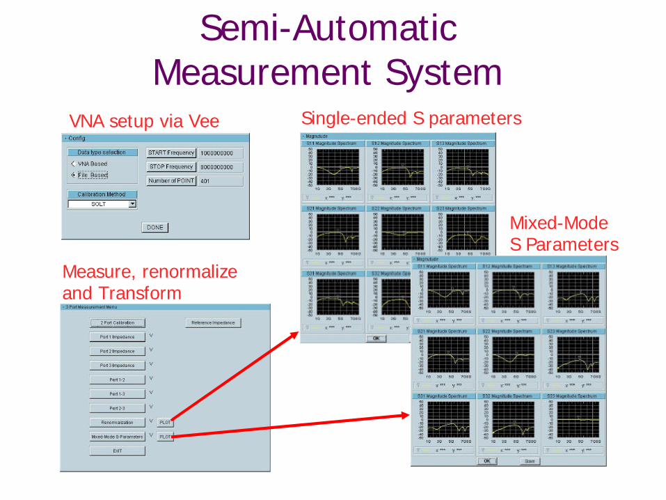
Semi-Automatic Measurement System
VNA setup via Vee
Measure, renormalize and Transform
Single-ended S parameters
Mixed-Mode S Parameters

Application to On-Wafer Measurement
$JLOHQW
$JLOHQW
91$
$JLOHQW
Our proposed System System made by NIST

Conclusions
Ø Various types of LTCC Embedded Inductors have been designed and measured. Simulated results agree with measurements quite well.
Ø A new modified-T equivalent circuit has been proposed to model LTCC inductors over an extremely large bandwidth successfully.
Ø Very cost-effective multiport network analyzer system based on renormalization techniques has been developed to measure balanced devices.
Ø Several examples of multiport and balanced devices on PCB have been designed and measured. Comparison between simulation and measurement shows excellent agreement.

References
1. K. Lim, et. al., “RF-system-on-package (SOP) for wireless communications,” IEEE Microwave Magazine, pp. 88-99, March 2002.
2. J.C. Tippet and R.A. Speciale, “A rigorous technique for measuring the scattering matrix of a multiport device with a 2-port network analyzer,” IEEE Transactions on Microwave Theory and Techniques, pp. 661-666, May 1982.
3. L.-Q. Yang, Design and modeling of embedded inductors and capacitors in low-temperature cofired ceramic technology, Master’s Thesis, National Sun Yat-Sen University at KaohsiungTaiwan, 2002.
4. D.-C. Tsai, Measurement of balanced devices using vector network analyzers, Master’s Thesis, National Sun Yat-Sen University at Kaohsiung, Taiwan, 2002.