product specification 1 - nordic semiconductor · nrf8002 product specification ... sms and, calls....
TRANSCRIPT

All rights reserved.Reproduction in whole or in part is prohibited without the prior written permission of the copyright holder.
2013-09-16
nRF8002
Single-chip Bluetooth® Low Energy Proximity Solution
Product Specification 1.1
Key Features
• Fully qualified Bluetooth low energy 4.0 peripheral device
• Single chip solution for Bluetooth low energy proximity applications
• Integrated Bluetooth low energy profiles and services
• Configurable I/Os for application behavior• Ultra-low power consumption• Coin-cell battery operation• Low cost 16 MHz ±50 ppm crystal• On-chip 32 kHz RC oscillator• Single 1.9-3.6 V power supply• Low cost external BOM• Temperature range -25 to +70°C • Compact 5x5 mm QFN32 package• RoHS compliant
Applications
• Proximity applications• Key fobs• Watches

nRF8002 Product Specification
Liability disclaimer
Nordic Semiconductor ASA reserves the right to make changes without further notice to the product to improve reliability, function or design. Nordic Semiconductor ASA does not assume any liability arising out of the application or use of any product or circuits described herein.
Life support applications
Nordic Semiconductor’s products are not designed for use in life support appliances, devices, or systems where malfunction of these products can reasonably be expected to result in personal injury. Nordic Semiconductor ASA customers using or selling these products for use in such applications do so at their own risk and agree to fully indemnify Nordic Semiconductor ASA for any damages resulting from such improper use or sale.
Contact details
For your nearest dealer, please see www.nordicsemi.com
Main office:
Otto Nielsens veg 127004 Trondheim
Phone: +47 72 89 89 00 Fax: +47 72 89 89 89www.nordicsemi.com
Datasheet status
Objective Product Specification This product specification contains target specifications for product development.
Preliminary Product Specification This product specification contains preliminary data; supplementary data may be published from Nordic Semiconductor ASA later.
Product Specification This product specification contains final product specifications. Nordic Semiconductor ASA reserves the right to make changes at any time without notice in order to improve design and supply the best possible product.
Page 2 of 46Revision 1.1

nRF8002 Product Specification
RoHS statement
Nordic Semiconductor’s products meet the requirements of Directive 2002/95/EC of the European Parliament and of the Council on the Restriction of Hazardous Substances (RoHS). Complete hazardous substance reports as well as material composition reports for all active Nordic Semiconductor products can be found on our website www.nordicsemi.com.
Revision History
Date Version Description
September 2013 1.1 • Updated section 10.1 on page 35 and chapter 15 on page 43.• Fixed minor issues throughout the document.
August 2012 1.0 • First release of the Product Specification (PS).• Renamed pin 32 from DCC to NC, see Figure 2. on page 7.• Changed application behavior, when the peer terminates the
connection, the nRF8002 goes into connecting state, see Figure 4. on page 11.
• Added chapter 2 on page 6, Bluetooth Qualification ID.• Added section 6.4 on page 29, Configuration in production• Fixed minor issues throughout the document.
February 2012 0.7 • First release of the Preliminary Product Specification (PPS)
Page 3 of 46Revision 1.1

nRF8002 Product Specification
Contents
1 Introduction . . . . . . . . . . . . . . . . . . . . . . . . . . . . . . . . . . . . . . . . . . . . . . . . . . . . 52 Bluetooth Qualification ID . . . . . . . . . . . . . . . . . . . . . . . . . . . . . . . . . . . . . . . . 63 Pin assignment . . . . . . . . . . . . . . . . . . . . . . . . . . . . . . . . . . . . . . . . . . . . . . . . . 73.1 Pin functions . . . . . . . . . . . . . . . . . . . . . . . . . . . . . . . . . . . . . . . . . . . . . . . . 84 Operation . . . . . . . . . . . . . . . . . . . . . . . . . . . . . . . . . . . . . . . . . . . . . . . . . . . . . . 94.1 Power up. . . . . . . . . . . . . . . . . . . . . . . . . . . . . . . . . . . . . . . . . . . . . . . . . . . 94.2 Power up sequence flow chart . . . . . . . . . . . . . . . . . . . . . . . . . . . . . . . . 104.3 State diagram . . . . . . . . . . . . . . . . . . . . . . . . . . . . . . . . . . . . . . . . . . . . . . 115 nRF8002 profiles and services. . . . . . . . . . . . . . . . . . . . . . . . . . . . . . . . . . . . 125.1 Generic Access Profile (GAP) parameters . . . . . . . . . . . . . . . . . . . . . . . . 125.2 Profiles and services. . . . . . . . . . . . . . . . . . . . . . . . . . . . . . . . . . . . . . . . . 126 nRF8002 configuration . . . . . . . . . . . . . . . . . . . . . . . . . . . . . . . . . . . . . . . . . . 146.1 Profile and Service configuration . . . . . . . . . . . . . . . . . . . . . . . . . . . . . . . 146.2 Input Signals (ISIG) . . . . . . . . . . . . . . . . . . . . . . . . . . . . . . . . . . . . . . . . . 176.3 Output signals (OSIG) . . . . . . . . . . . . . . . . . . . . . . . . . . . . . . . . . . . . . . . 206.4 Configuration in production. . . . . . . . . . . . . . . . . . . . . . . . . . . . . . . . . . . . 297 Direct Test Mode (DTM) . . . . . . . . . . . . . . . . . . . . . . . . . . . . . . . . . . . . . . . . . 327.1 Activating and deactivating Direct Test Mode. . . . . . . . . . . . . . . . . . . . . . 327.2 Transmitter constant carrier operation . . . . . . . . . . . . . . . . . . . . . . . . . . . 328 Absolute maximum ratings . . . . . . . . . . . . . . . . . . . . . . . . . . . . . . . . . . . . . . 339 Operating conditions . . . . . . . . . . . . . . . . . . . . . . . . . . . . . . . . . . . . . . . . . . . 3410 Electrical specifications . . . . . . . . . . . . . . . . . . . . . . . . . . . . . . . . . . . . . . . . . 3510.1 Digital I/O signal levels . . . . . . . . . . . . . . . . . . . . . . . . . . . . . . . . . . . . . . . 3510.2 Radio characteristics . . . . . . . . . . . . . . . . . . . . . . . . . . . . . . . . . . . . . . . . 3610.3 Analog feature characteristics . . . . . . . . . . . . . . . . . . . . . . . . . . . . . . . . . 3711 Current consumption . . . . . . . . . . . . . . . . . . . . . . . . . . . . . . . . . . . . . . . . . . . 3812 Hardware description . . . . . . . . . . . . . . . . . . . . . . . . . . . . . . . . . . . . . . . . . . . 3912.1 Reset . . . . . . . . . . . . . . . . . . . . . . . . . . . . . . . . . . . . . . . . . . . . . . . . . . . . 3912.2 16 MHz oscillator . . . . . . . . . . . . . . . . . . . . . . . . . . . . . . . . . . . . . . . . . . . 3912.3 UART interface characteristics . . . . . . . . . . . . . . . . . . . . . . . . . . . . . . . . . 4012.4 Antenna matching and balun . . . . . . . . . . . . . . . . . . . . . . . . . . . . . . . . . . 4012.5 PCB layout and decoupling guidelines . . . . . . . . . . . . . . . . . . . . . . . . . . . 4013 Mechanical specifications . . . . . . . . . . . . . . . . . . . . . . . . . . . . . . . . . . . . . . . 4114 Ordering information . . . . . . . . . . . . . . . . . . . . . . . . . . . . . . . . . . . . . . . . . . . 4214.1 Package marking . . . . . . . . . . . . . . . . . . . . . . . . . . . . . . . . . . . . . . . . . . . 4214.2 Abbreviations . . . . . . . . . . . . . . . . . . . . . . . . . . . . . . . . . . . . . . . . . . . . . . 4214.3 Product options. . . . . . . . . . . . . . . . . . . . . . . . . . . . . . . . . . . . . . . . . . . . . 4215 Example application circuitry . . . . . . . . . . . . . . . . . . . . . . . . . . . . . . . . . . . . 4315.1 PCB guidelines . . . . . . . . . . . . . . . . . . . . . . . . . . . . . . . . . . . . . . . . . . . . . 4315.2 Schematic nRF8002 example application . . . . . . . . . . . . . . . . . . . . . . . . 4315.3 PCB layout nRF8002 example application . . . . . . . . . . . . . . . . . . . . . . . . 4415.4 Bill of Materials nRF8002 example application. . . . . . . . . . . . . . . . . . . . . 4516 Glossary . . . . . . . . . . . . . . . . . . . . . . . . . . . . . . . . . . . . . . . . . . . . . . . . . . . . . . 46
Page 4 of 46Revision 1.1
nRF8002 Product Specification
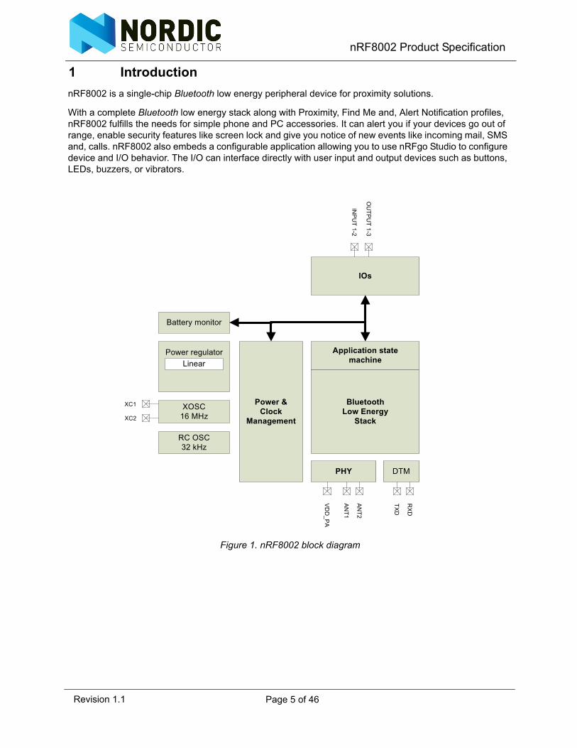
1 Introduction
nRF8002 is a single-chip Bluetooth low energy peripheral device for proximity solutions.
With a complete Bluetooth low energy stack along with Proximity, Find Me and, Alert Notification profiles, nRF8002 fulfills the needs for simple phone and PC accessories. It can alert you if your devices go out of range, enable security features like screen lock and give you notice of new events like incoming mail, SMS and, calls. nRF8002 also embeds a configurable application allowing you to use nRFgo Studio to configure device and I/O behavior. The I/O can interface directly with user input and output devices such as buttons, LEDs, buzzers, or vibrators.
Figure 1. nRF8002 block diagram
IOs
XOSC16 MHz
BluetoothLow Energy
Stack
PHY
RC OSC32 kHz
DTM
Power & Clock
Management
Power regulator
Linear
Battery monitor
Application state machine
XC1
XC2
INP
UT
1-2
OU
TP
UT
1-3
VD
D_P
A
AN
T1
AN
T2
TX
D
RX
D
Page 5 of 46Revision 1.1

nRF8002 Product Specification
2 Bluetooth Qualification ID
nRF8002 is listed as an EP-QDL on the Qualified listings page of the Bluetooth Special Interest Group website https://www.bluetooth.org/tpg/listings.cfm.
For details on the design qualifications, please refer to the following qualification IDs:
• B019507 - nRF8002, End Product, Single-chip Bluetooth low energy proximity solution.• B019124 - uBlue Host 1.2, Nordic Bluetooth Low Energy Host Layer version 1.2.• B016981 - Nordic µBlue LL, BTLE link layer stack component.• B019518 - nRF8002_RF, Bluetooth low energy HW platform containing the RF PHY layer for the
nRF8002 system on chip device.
Page 6 of 46Revision 1.1

nRF8002 Product Specification
3 Pin assignment
nRF8002 is available in a 5x5 mm QFN32 package. The back plate of the QFN32 capsule must be grounded to the application PCB in order to achieve optimal performance. The physical dimensions of the QFN32 are presented in chapter 13 on page 41.
Figure 2. shows the pin assignment for nRF8002 and Table 1. on page 8 describes the pin functionality.
Figure 2. nRF8002 pin assignment (top view)
exposed die pad
1
2
3
4
5
6
7
8
13 14 15 169 10 11 12
17
18
19
20
21
22
23
24
252627
2829303132VDD
DEC1
DEC2
VDD
INPUT1
VSS
OUTPUT1
OUTPUT2
AVDD
VSS
ANT2
ANT1
VDD_PA
RESET
VSS
NC
XC1
XC2
AVDD
IREF
nRF8002QFN32(5x5 mm)
VSSVSS
PWM
AVDD
VSS
VSS
INPUT2
OUTPUT3
TXD
RXD
VSS
VSS
Page 7 of 46Revision 1.1
nRF8002 Product Specification
3.1 Pin functions
Table 1. nRF8002 pin functions
Pin Pin name Pin functions Description
1 VDD Power Power supply (1.9 – 3.6 V)2 DEC1 Power Regulated power supply output for decoupling purposes only.
Connect 100 nF capacitor to ground3 DEC2 Power Regulated power supply output for decoupling purposes only.
Connect 33 nF capacitor to ground4 VSS Power Ground (0V)5 VSS Power Ground (0V)6 PWM Digital output Programmable PWM output (range 490 Hz….516 kHz)7 TXD Digital output UART (transmit) for Bluetooth low energy Direct Test Mode
Interface and for configuration download. After final OTP program of configuration, pin must be set to VSS.
8 VSS Power Ground (0V)9 VDD Power Power supply (1.9 – 3.6 V)
10 RXD Digital input UART (receive) for Bluetooth low energy Direct Test Mode Interface and for configuration download. After final OTP program of configuration, pin must be set to VSS.
11 INPUT1 Digital input General input (if not in use this pin must be set to VSS)12 INPUT2 Digital input General input (if not in use this pin must be set to VSS)13 VSS Power Ground (0V)14 OUTPUT1 Digital output General output15 OUTPUT2 Digital output General output16 OUTPUT3 Digital output General output17 VSS Power Ground (0V)18 VSS Power Ground (0V)19 RESET Digital input Reset (active low)20 VDD_PA Power output Regulated power supply output for on-chip RF Power amplifier21 ANT1 RF Differential antenna connection (TX and RX)22 ANT2 RF Differential antenna connection (TX and RX)23 VSS Power Ground (0V)24 AVDD Power Analog power supply (1.9 – 3.6 V DC)25 IREF Analog output Current reference terminal.
Connect a 22 kΩ 1% resistor to ground26 AVDD Power Analog power Supply (1.9 – 3.6 V)27 XC2 Analog output Connection for 16 MHz crystal oscillator.
Leave unconnected if not in use28 XC1 Analog input Connection for 16 MHz crystal or external 16 MHz reference29 AVDD Power Analog power supply (1.9 – 3.6 V DC)30 VSS Power Ground (0V)31 VSS Power Ground (0V)32 NC - Not connected
Exposed die pad
VSS Power Ground (0V), connect to VSS
Page 8 of 46Revision 1.1

nRF8002 Product Specification
4 Operation
This chapter describes the power-up sequence for nRF8002 and the modes it can enter and also a state diagram that illustrates the operating states and their behavior. Configuration data can be stored in RAM or non-volatile memory (also called One Time Programmable memory, or OTP) in nRF8002.
4.1 Power up
Power up is defined as when nRF8002 is powered up for the first time (the battery is inserted) or the chip is reset. When nRF8002 is powered up its behavior depends on whether a custom configuration has been pre-programmed into the non-volatile memory (OTP). If the OTP contains a valid configuration, nRF8002 starts with these configuration settings and is ready for operational use.
In Configuration mode, nRF8002 can receive the configuration generated by nRFgo Studio. The nRF8002 configuration decides profile, application and I/O behavior. RAM is used during development to enable repeated configuration downloads. Each time nRF8002 is reset, or power is removed, it returns to a non-configured state and you can choose to enter DTM or download a new configuration.
If there is no valid configuration available in OTP, nRF8002 will start in either Direct Test Mode (DTM) or Configuration mode, depending on the first byte received on the UART:
• If the first byte received on the UART is 0xFF, nRF8002 starts in Configuration mode.• If the first byte received on the UART is NOT 0xFF, nRF8002 starts in DTM mode.
See chapter 7 on page 32 for more information on DTM.
Note: When the chip is in DTM or Configuration mode it will rapidly drain the battery, as it does not use power management in these modes.
Once development is finished final configuration can be downloaded to non-volatile memory (OTP) from nRFgo studio or saved to file for use in factory programming tools.
Note: If configuration is programmed into OTP, DTM mode is no longer accessible.
When the configuration is available in OTP, the UART is disabled.
Page 9 of 46Revision 1.1

nRF8002 Product Specification
4.2 Power up sequence flow chart
Figure 3. Power up sequence flow chart
Is Configin OTP?
Power on or Reset
Is firstbyte on UART
0xFF?
DTM modeConfig mode
Write toOTP or RAM?
Write to RAMWrite to OTP
NoYes
NoYes
Run
RAMOTP
Page 10 of 46Revision 1.1
nRF8002 Product Specification
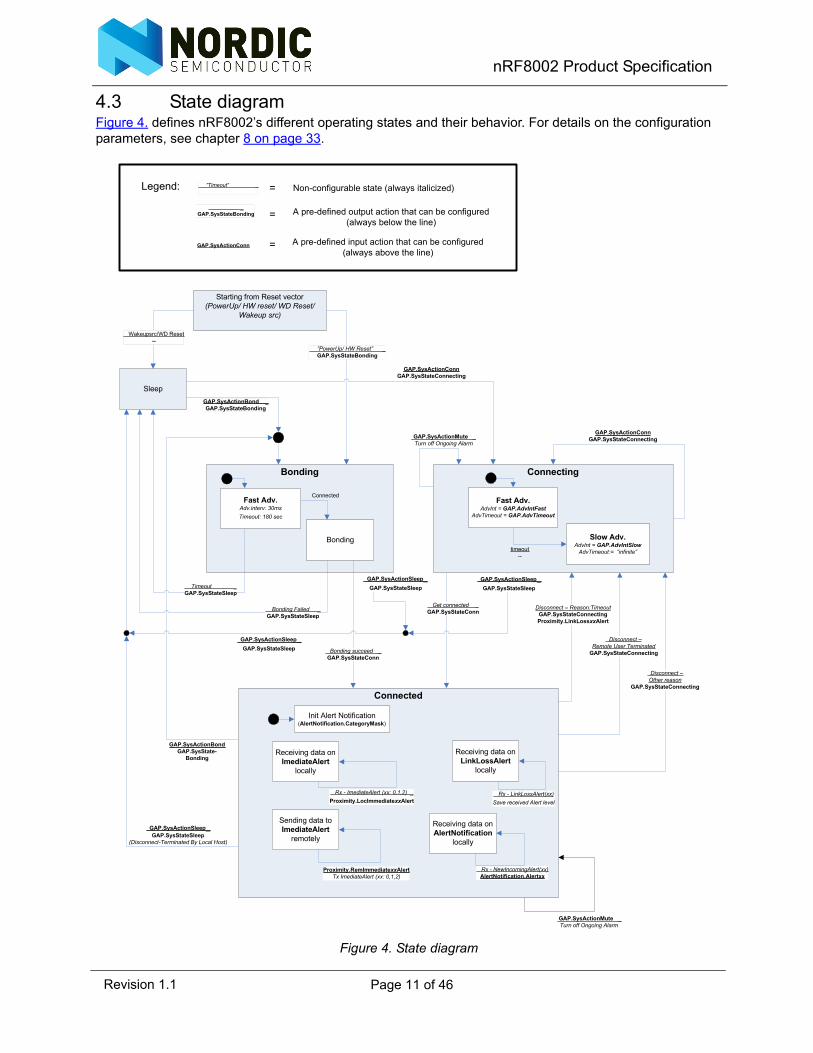
4.3 State diagramFigure 4. defines nRF8002’s different operating states and their behavior. For details on the configuration parameters, see chapter 8 on page 33.
Figure 4. State diagram
”PowerUp/ HW Reset” _GAP.SysStateBonding
Sleep
GAP.SysActionBond _ GAP.SysStateBonding
Bonding
GAP.SysActionConnGAP.SysStateConnecting
Timeout _GAP.SysStateSleep
Get connected _GAP.SysStateConn
Bonding succeed _GAP.SysStateConn
Connecting
Connected
Fast Adv.AdvInt = GAP.AdvIntFast
AdvTimeout = GAP.AdvTimeout
Slow Adv.AdvInt = GAP.AdvIntSlow
AdvTimeout:= ”infinite”timeout--
GAP.SysActionConnGAP.SysStateConnecting
Fast Adv.Adv.interv: 30ms
Timeout: 180 sec
Bonding
Connected
Bonding Failed _GAP.SysStateSleep
Disconnect –Remote User Terminated
GAP.SysStateConnecting
Receiving data onImediateAlert
locally
Rx - ImediateAlert (xx: 0,1,2) _
Proximity.LocImmediatexxAlert
Sending data toImediateAlert
remotely
Proximity.RemImmediatexxAlertTx ImediateAlert (xx: 0,1,2)
Disconnect – Reason:TimeoutGAP.SysStateConnectingProximity.LinkLossxxAlert
Receiving data onAlertNotification
locally
Rx - NewIncomingAlert(xx)AlertNotification.Alertxx
Receiving data onLinkLossAlert
locally
Rx - LinkLossAlert(xx)
Save received Alert level
Init Alert Notification(AlertNotification.CategoryMask)
GAP.SysActionSleep_GAP.SysStateSleep
(Disconnect-Terminated By Local Host)
GAP.SysActionBondGAP.SysState-
Bonding
GAP.SysActionSleep_GAP.SysStateSleep
GAP.SysActionMute _Turn off Ongoing Alarm
GAP.SysActionMute _Turn off Ongoing Alarm
Starting from Reset vector(PowerUp/ HW reset/ WD Reset/
Wakeup src)
Wakeupsrc/WD Reset --
GAP.SysActionSleep_GAP.SysStateSleep
GAP.SysActionSleep_GAP.SysStateSleep
Disconnect –Other reason
GAP.SysStateConnecting
”Timeout” _ = Non-configurable state (always italicized)
_GAP.SysStateBonding = A pre-defined output action that can be configured
(always below the line)
GAP.SysActionConn = A pre-defined input action that can be configured(always above the line)
Legend:
Page 11 of 46Revision 1.1

nRF8002 Product Specification
5 nRF8002 profiles and services
nRF8002 offers Battery Status, TX power, Link Loss and, Immediate Alert services. It also implements the Find Me and Alert Notification profiles for use with a peer device that supports Alert Notification and Immediate Alert services. When a connection is established with a peer device, nRF8002 automatically performs the service discovery and enables the corresponding application functionality.
5.1 Generic Access Profile (GAP) parameters
nRF8002 implements the Generic Access Profile (GAP) using the following parameters, (see chapter 6.1 on page 14 for more information):
• Configurable advertising intervals• Device name characteristic• Device security: Just Works• Minimum encryption key size: 7 bytes• Maximum encryption key size: 16 bytes• TX power• Preferred peripheral connection parameters characteristic
When a connection is established but the connection interval is not within the set parameters, nRF8002 responds by initiating the Connection Parameter Update procedure as described in the Bluetooth Core Specification Ver. 4.0, Vol. 3.0, Part C, GAP, section 9.3.9. If the peer does not change the connecting interval, nRF8002 will disconnect.
5.2 Profiles and services
This section describes the services that are available on nRF8002, and the services it will try to discover on a peer device.
5.2.1 nRF8002 local services
The service and characteristics that are available on nRF8002 are defined in Table 2. below.
Attribute type UUID Value Properties
Primary Service 0x2800 GAP (0x1800) ReadCharacteristic Declaration 0x2803 Device Name (0x2A00) Read
Characteristic Value - Device Name 0x2A00 “nRF8002” Read/WriteCharacteristic Declaration 0x2803 Appearance (0x2A01) Read
Characteristic Value - Appearance 0x2A01 0x0000 ReadCharacteristic Declaration 0x2803 PPCP (0x2A04) Read
Characteristic Value – PPCP 0x2A04 Conn min, Conn max,
Slave Latency, Timeout
Read
Primary Service 0x2800 GATT (0x1801) Read
Primary Service 0x2800 DEVICE INFORMATION (0x180A)
Read
Characteristic Declaration 0x2803 Manufacturer Name (0x2A29) ReadCharacteristic Value – Manufacturer
Name0x2A29 “NordicSemi” Read
Characteristic Declaration 0x2803 Model Number (0x2A24) ReadCharacteristic Value – Model Number 0x2A24 “nRF8002” Read
Characteristic Declaration 0x2803 Firmware revision (0x2A26) Read
Page 12 of 46Revision 1.1

nRF8002 Product Specification
Table 2. Services and characteristics on nRF8002
5.2.2 nRF8002 profiles and remote servicesnRF8002 automatically carries out service discovery on a peer device and attempts to discover the services defined in Table 3.
Table 3. Supported services/characteristics on a peer device
Characteristic Value – Firmware revision
0x2A26 This will be set to the nRF8002 firmware version number
Read
Characteristic Declaration 0x2803 Software revision (0x2A28) ReadCharacteristic Value – Software
revision0x2A28 Configurable by nRFgo Studio Read
Primary Service 0x2800 IMMEDIATE ALERT (0x1802) ReadCharacteristic Declaration 0x2803 Alert Level (0x2A06) Read
Characteristic Value – Alert Level 0x2A06 <Value> Read/ WriteWithoutResponse
Primary Service 0x2800 LINK LOSS (0x1803) ReadCharacteristic Declaration 0x2803 Alert Level (0x2A06) Read
Characteristic Value – Alert Level 0x2A06 <Value> Read/WritePrimary Service 0x2800 TX POWER (0x1804) Read
Characteristic Declaration 0x2803 TxPower (0x2A07) ReadCharacteristic Value – TxPower 0x2A07 <0x00> Read
Primary Service 0x2800 BATTERY (0x180F) ReadCharacteristic Declaration 0x2803 BatteryLevel (0x2A19) Read
Characteristic Value – BatteryLevel 0x2A19 0x64 (=100%) Read/NotifyChar Descriptor - CCCD 0x2902 < Configuration> Read/Write
Attribute type UUID Value Properties
Primary Service 0x2800 GATT (0x1801) ReadCharacteristic Declaration 0x2803 Service Changed (0x2A05) Read
Characteristic Value – Service Changed 0x2A05 <... Service change values …> IndicateChar Descriptor – CCCD 0x2902 <Configuration> Read/ Write
Primary Service 0x2800 IMMEDIATE ALERT (0x1802) ReadCharacteristic Declaration 0x2803 Alert Level (0x2A06) Read
Characteristic Value – Alert Level 0x2A06 <Value> Read/ WriteWithoutRe
sponsePrimary Service 0x2800 ALERT NOTIFICATION
(0x1811)Read
Characteristic Declaration 0x2803 Supported New Alert Category (0x2A47)
Read
Characteristic Value – Supported New Alert Category
0x2A47 <Value> Read
Characteristic Declaration 0x2803 New Alert (0x2A46) ReadCharacteristic Value –
New Alert0x2A46 <0x00> Notify
Char Descriptor – CCCD 0x2902 <Configuration> Read/ WriteCharacteristic Declaration 0x2803 Alert Notification Control Point
(0x2A44)Read
Characteristic Value – Alert Notification Control Point
0x2A44 <0x00> Write
Attribute type UUID Value Properties
Page 13 of 46Revision 1.1

nRF8002 Product Specification
6 nRF8002 configuration
Profiles and services are pre-defined on nRF8002 but, you can configure input signals to generate pre-defined GAP behavior and pre-defined actions related to Profiles and Services. Output signals can be configured to generate patterns on pre-defined events that are related to Services, Profiles and, GAP behavior.
nRF8002 must be configured using the nRFgo Studio v1.12.3 or later. The configuration is downloaded through the UART, either directly from nRFgo Studio or by using the Production configuration tool available from Nordic Semiconductor. When downloading, you can choose to load the configuration into volatile memory (RAM) for development purposes or non-volatile memory (OTP) for production.
Note: If loaded into non-volatile memory (OTP) you cannot reconfigure nRF8002.
nRF8002 can be configured to respond to different input pin pulses and to issue different output patterns depending on the Bluetooth service and profile behavior.
Use the nRF8002 configuration tool in nRFgo Studio to change and download new configurations that match your application needs by setting the configuration in RAM. A default configuration is available in nRFgo Studio for download to your nRF8002 device. The default configuration is made to work with the development kit.
6.1 Profile and Service configuration
nRF8002 contains an integrated set of Bluetooth profiles and services. The application behavior of these profiles and services can be connected to Input signal (ISIG) and Output signal (OSIG) events.
6.1.1 General settings
6.1.1.1 Generic Access Profile (GAP) and hardware settings
nRF8002 allows the following configuration of hardware and GAP settings through the nRFgo Studio:
Table 4. GAP and hardware configuration settings
Name Resolution Description
GAP.LocalName N/A Local Name of the device: 0 - 20 bytes (UTF-8 sting) (no null termination)
GAP.Appearance N/A Appearance characteristic
GAP.TxPowerConn N/A Output Power of nRF8002 in connection or advertising to a bonded device, Steps: -18, -12, -6, 0 dBm
GAP.AdvIntSlow 625 µs Background advertising Interval - Slow Adv.n – Background (Range:32…16384)
GAP.AdvIntFast 625 µs Fast advertising Interval - Fast Adv.n – Fast (Range: 32…16384)
GAP.AdvTimeout 1 s Timeout for Fast Adv.Up to 180 sec, 1 sec resolution. Only available in connecting state.
GAP.ConnIntMin 1.25 ms Minimum Connection Interval: 250 ms – 2 sec, must be less than GAP.ConnIntMax
GAP.ConnIntMax 1.25 ms Maximum connection Interval: 250 ms – 2 sec, must be more than GAP.ConnIntMin + 12.5 ms
GAP.ConnTimeout 1.25 ms Connection Supervision Timeout.
Page 14 of 46Revision 1.1
nRF8002 Product Specification
6.1.1.2 GAP state to OSIG configuration
nRF8002 allows the following configuration of OSIG events when entering the different states defined in GAP through the nRFgo Studio:
Table 5. GAP state to OSIG Configuration
6.1.1.3 GAP state to ISIG configuration
nRF8002 allows the following configuration of ISIG events to enter different GAP states through the nRFgo Studio:
Table 6. GAP state to ISIG Configuration
6.1.2 Profiles
6.1.2.1 Device information settings
nRF8002 allows the following configuration of Device Information settings through the nRFgo Studio:
Table 7. Description of device information settings
Name Action
GAP.SysStateBonding Output Pin, pattern number, inverted, enable/disableGAP.SysStateConnecting Output Pin, pattern number, inverted, enable/disableGAP.SysStateConnected Output Pin, pattern number, inverted, enable/disable
Name Action
GAP.SysActionBond Input pin, Press Event GAP.SysActionConnecting Input pin, Press Event GAP.SysActionSleep Input pin, Press EventGAP.SysActionMute Input pin, Press Event
Name Units Description
DeviceInfo.ManufacturerName n/a The name of the manufacturer of the device0 - 20 bytes (no null termination)
DeviceInfo.ModelNumbern/a
The model number that is assigned by the device vendor0 - 20 bytes (no null termination)
DeviceInfo.FirmwareRevision n/a The firmware revision of the nRF8002 device (this is non-configurable)
DeviceInfo.SoftwareRevision n/a The Software revision of the device
Page 15 of 46Revision 1.1

nRF8002 Product Specification
6.1.2.2 nRF8002 profile and service behavior to OSIG configuration
The Proximity Alert settings (OSIG) define the output pins that are triggered on the different alarms.
Table 8. Profile and service behavior to OSIG Configuration (OSIG)
6.1.2.3 nRF8002 profile and service behavior to ISIG configuration
The Proximity signaling actions (ISIG) define which input signals should be used to send an alarm:
Table 9. Profile and service behavior to ISIG Configuration (ISIG)
Name Action
Proximity.LinkLossMildAlert Output pin, pattern number, inverted, enable/disable. Link Loss with Mild Alert active.
Proximity.LinkLossHighAlert Output pin, pattern number, inverted, enable/disable. Link Loss with High Alert active.
Proximity.LocImmediateOffAlert Output pin, pattern number, inverted, enable/disable. Local Off Alert.
Proximity.LocImmediateMildAlert Output pin, pattern number, inverted, enable/disable. Local Mild Alert.
Proximity.LocImmediateHighAlert Output pin, pattern number, inverted, enable/disable. Local High Alert.
AlertNotification.CategoryMask See Alert Notification Service (0 disables all alerts) (UINT16 bit mask).
AlertNotification.Alert 1 AlertCategory Id bit mask to set which Category that should trigger this OSIG.
….AlertNotification.Alert 4 AlertCategory Id bit mask to set which
Category that should trigger this OSIG.
Name Description
Proximity.RemImmediateOffAlert Input pin, Press EventTrigger Remote Off Alert
Proximity.RemImmediateMildAlert Input pin, Press EventTrigger Remote Mild Alert
Proximity.RemImmediateHighAlert Input pin, Press EventTrigger Remote High Alert
Page 16 of 46Revision 1.1
nRF8002 Product Specification
6.1.2.4 Battery configuration
The battery voltage level defines when an alarm will be triggered:
Table 10. Battery configuration
6.1.2.5 Mute
The mute action lets a user stop a OSIG event (for example, to silence an audible alarm). You can configure which input signal generates the mute action and which Output signal(s) that is turned off by this action.
The mute action is only available when nRF8002 is in connected mode.
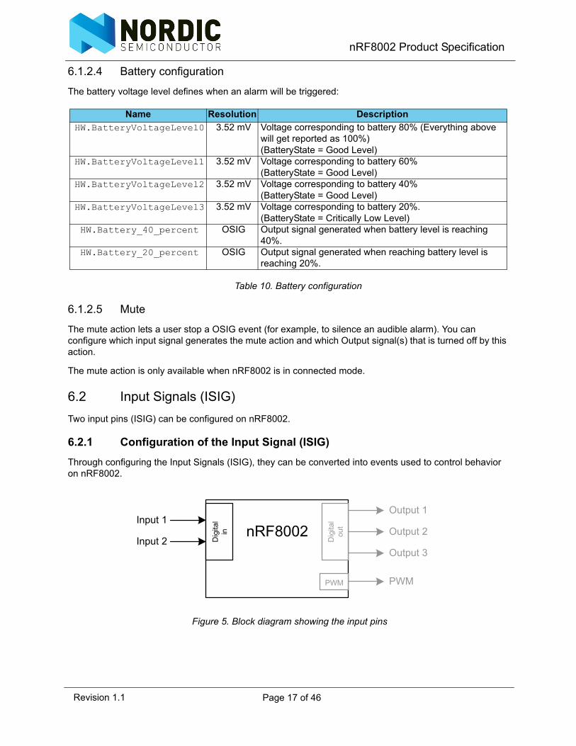
6.2 Input Signals (ISIG)
Two input pins (ISIG) can be configured on nRF8002.
6.2.1 Configuration of the Input Signal (ISIG)
Through configuring the Input Signals (ISIG), they can be converted into events used to control behavior on nRF8002.
Figure 5. Block diagram showing the input pins
Name Resolution Description
HW.BatteryVoltageLevel0 3.52 mV Voltage corresponding to battery 80% (Everything above will get reported as 100%)(BatteryState = Good Level)
HW.BatteryVoltageLevel1 3.52 mV Voltage corresponding to battery 60% (BatteryState = Good Level)
HW.BatteryVoltageLevel2 3.52 mV Voltage corresponding to battery 40%(BatteryState = Good Level)
HW.BatteryVoltageLevel3 3.52 mV Voltage corresponding to battery 20%. (BatteryState = Critically Low Level)
HW.Battery_40_percent OSIG Output signal generated when battery level is reaching 40%.
HW.Battery_20_percent OSIG Output signal generated when reaching battery level is reaching 20%.
nRF8002 Output 2
Output 3
PWM
Output 1
Dig
ital
out
PWM
Input 2
Input 1
Dig
ital
in
Page 17 of 46Revision 1.1

nRF8002 Product Specification
6.2.2 Input polarity
The input polarity can be set individually for each of the input pins. Table 11. below describes the expected behavior (Input Signal).
Table 11. Input signal behavior
6.2.3 Events generated from the inputs
Each input line can generate the following four events:
• Activation Trigger Event• Short Press Event• Medium Press Event• Long Press Event
The Activation Trigger Event is generated every time the input line is activated (see section 6.2.2 on page 18). Depending on the time it takes before the input line is released (length of the pulse), nRF8002 will generate one of three events: a Short, Medium, or a Long press event. Minimum time before an input is released is 50 ms, for detection of a valid trigger and subsequently a press event.
For nRF8002 to distinguish between these three events, the user has to specify two timer values, as defined in Table 12. The two timer values are common for both input lines.
Table 12. Timer values
Polarity Input signal Schematic Description
Active High
The input line is initiated by a VSS-to-VDD transition. The input pin is configured to logic level 0 using an internal pull down resistor.
Active Low
The input line is initiated by a VDD-to-VSS transition. The input pin is configured to logic level 1 using an internal pull up resistor.
Timer Description
t1 Distinguishes between a short and a medium press. t2 Distinguishes between a medium and a long press.
[VSS]
[VDD]
Activate
Re
lease
V ss
Vdd
INPUT
Input x
DIGITAL
INPUT
[VSS]
[VDD]
Activate
Re
lease
V ss
Input xDIGITALINPUT
Vdd
Page 18 of 46Revision 1.1

nRF8002 Product Specification
Decoding an input pulse using t1 and t2 will generate the following event:
• All pulses will generate an Activation Trigger event at the start of the pulse.• An input pulse that has ended before reaching t1 will be decoded as a Short Press.• An input pulse that is active when reaching t1 but has ended before reaching t2 will be decoded as
a Medium Press.• An input pulse that is active when reaching t2 will be decoded as Long Press.
6.2.4 OSIG events generated by the inputs
Generating an OSIG event from an input signal is a good way to give a user feedback that is related to the length of the pulse they have activated.
Each of the two input lines on the device has two OSIG events. The first OSIG event is generated when the input line has been active for a period equal to t1, the second OSIG event is generated when the input line has been active for a period equal to t2.
See Table 14. on page 21 for a list of the events. For configuration of the OSIG events see section 6.3.5 on page 27, OSIG activation.
6.2.4.1 Example showing ISIG event and OSIG action
Table 13. ISIG event and OSIG activation from Activation trigger and short, medium and, long press
Input pulse Description
• Input pulse shorter than t1.• Gives an Activation trigger event at the start of
the pulse.• Gives a Short Press Event at the end of the
pulse.• OSIG Activation: none.
• Input pulse longer than t1, but shorter than t2.• Gives an Activation trigger event at the start of
the pulse.• OSIG Activation: Input x –t1 when the time t1 is
reached.• Gives a Medium Press Event at the end of the
pulse.
• Input pulse longer than t2.• Gives an Activation trigger event at the start of
the pulse.• OSIG Activation: Input x –t1 when the time t1 is
reached.• OSIG Activation: Input x –t2 when the time t2 is
reached.• Gives a Long Press Event at the end of the
pulse.
Edge trig
t1
t2
Short Press
time
ShortpressISIG Events:
OSIG Activation:
Edge trig
t1t2
Medium Press
time
ISIG Events: Mediumpress
OSIG Activation: Input x- t1
Edge trig
t1t2
Long Press
time
ISIG Events:
OSIG Activation: Input x- t1
Input x- t2
Longpress
Page 19 of 46Revision 1.1

nRF8002 Product Specification
6.3 Output signals (OSIG)
Four Output signals (OSIG), one of which is a PWM, can be configured on nRF8002. An Output signal (OSIG) is a Pulse Train pattern set on one of the four output pins.
6.3.1 Configuration of the Output signal (OSIG)
This section describes how the output ports are controlled by the configuration. The configuration of the output signals is defined as a Pulse Train and is defined by t1, t2 and, nt as documented in section 6.3.4 on page 23. The Pulse Train can be configured to repeat and is then defined as a Repeated Pulse Train. The action generating the OSIG is configurable and is linked to GAP, profile or, service behavior.
nRF8002 has four output ports where port 1 to 3 are digital outputs and port 4 is a PWM output, see Figure 6.
Figure 6. nRF8002’s output ports
As shown in Figure 7. on page 21, the output logic is divided into four different modules:
• OSIG Pattern: a set of logical pulse patterns that can be used to generate signals on the output ports.
• OSIG Activation: translates events into OSIG actions.• Output Handler: the engine that receives instructions from the OSIG Activation and uses this
together with the OSIG Pattern and the timer ticks to generate output action. • OSIG Output logic: translates the logical ON/OFF command received from the Output handler into
voltage level on the output ports. It also controls the PWM output signal.
Note: The OSIG Pattern, Activation, and Handler modules handle logical ON/OFF signals. The OSIG Output logic module translates the logical signal into a voltage level. This is done to separate the logical behavior from the physical representation on the output port.
nRF8002 Output 2
Output 3
PWM
Output 1
Dig
ital
PWM
Input 2
Input 1
Dig
ital
in
Page 20 of 46Revision 1.1

nRF8002 Product Specification
Figure 7. Output logic modules
6.3.2 Event table
Table 14. lists all the events that the user can configure to give an OSIG Activation.
Table 14. Event table
Event Description
Sleep State1
1. This event is hard-coded to turn OFF all output ports.
An event is generated when nRF8002 enters the given state.Bond StateConnecting StateConnected State
Link Loss Mild Alert One of these events could be generated when nRF8002 detects a link loss with Timeout. Which of the events depends on the Link Loss alert level set by the peer device.Link Loss High Alert
Immediate Alert – No Alert An event is generated when nRF8002 receives the corresponding Immediate Alert from the peer device.Immediate Alert – Mild Alert
Immediate Alert – High Alert
Battery Level 40% Events are generated every 10 minutes as long as the battery is on the actual level.Battery Level 20%
Alert Notification 0 Events are generated when nRF8002 receives an Alert Notification that matches the configuration set for the Alert Notification (See 6.1.2.2 on page 16).
Alert Notification 1Alert Notification 2Alert Notification 3
ISIG – Mute Action This event is generated by a ISIG event (as configured by the user)
ISIG Input 1 – t1 These events are given when the input port has been kept active for a period equal to the timer value (Used for giving feedback on a button press)
ISIG Input 1 – t2ISIG Input 2 – t1ISIG Input 2 – t2
OSIGOutput logic
OSIG Pattern(0..15)
Output handler
Fast Tick (50ms)
SlowTick (1 sec)
Output #
Pattern X
(Inverted Phase)OSIGActivation
On/ Off/
(Frequency) Vdd/ Vss
EVENTOutput 1Output 2Output 3
Output 4
Page 21 of 46Revision 1.1

nRF8002 Product Specification
6.3.3 OSIG output logic
The OSIG output logic is set individually for each of the four ports and specifies the translation from the logical representation (ON/OFF) to the voltage level (VDD/VSS). It specifies whether the logical value ON should set the port to high (VDD) or low (VSS).
For the PWM output port the frequency output will be set with 50% duty cycle when the port is ON. The first pulse will always be high (VDD).
Figure 8. Output logic on the digital and PWM ports
Figure 9. illustrates the behavior on the output pin related to the actual setting. The first row describes the behavior when the output is set to active high. Both the digital and the PWM output will then be set to VSS on Reset (power-up) and when it is set to OFF. When the output port is set ON the digital output will switch from VSS to VDD, while the PWM output will start oscillating at the specified frequency.
The second row in Figure 9. shows the reverse active low polarity.
Figure 9. PWM output voltage on active high and active low
Output portVDD
VSS
Logical level(ON/OFF)
ON
OFF
VddVssX
X
OFF
Output portVDD
VSS
Logical level(ON/OFF)
Output Port (PWM)
ON
OFF
VddVssX
X
OFF
PWMFreq.Logicaltranslation
Output Port (Digital)
Vdd
Vss
ONOFF
ONOFF
Vdd
Vss
DIGITAL OUTPUTVoltage on logical low PWM OUTPUT
ON
OFF
ON
OFF
Vdd
Vss
Vdd
Vss
50% 50%
tpwm
(1/tpwm=freq.)
VDD
VSS
Page 22 of 46Revision 1.1

nRF8002 Product Specification
6.3.4 OSIG pattern
The OSIG pattern is a table where the you can specify up to 15 different output patterns numbered from 1 to 15. It is also possible to invert a pattern during OSIG activation, see also Table 20. on page 27
Pattern 0 is predefined to a fixed level used to set the pin either permanently ON or OFF.
Table 15. Output patterns
The pattern specification is independent of the different output ports, that is, all patterns could be used on all the outputs.
The OSIG pattern is specified using timers (txx) and counters (nx). In addition, there is an optional parameter [fpwm] that specifies the frequency to be used in the ON period for the PWM output (Output port 4). This parameter will be ignored if the pattern is used on a digital output, but has to be specified for all patterns used on PWM.
The OSIG pattern can be specified using two different modes: Fast Tick or Slow Tick mode. The difference between them is the resolution for the two timers [tp1] and [tp2] that specifies the ON and OFF period.
No. tp1 tp2 np tt nt fpwm Description
0 1 0 0 0 0 0 Pre-configured to ON (OFF)1
Up to 15 patterns that should be configured by the customer
2…1415
Page 23 of 46Revision 1.1

nRF8002 Product Specification
Table 16. shows timers and counters that are defined as part of the OSIG Pattern definition:
Table 16. Timers and counters description
Parameter Value range Description
tp1 50 ms...12.75 sec1
1 sec…4 min15 sec1.
1. 50 ms or 1 second resolution depending on the mode (fast tick mode or slow tick mode).
Defines the period for when the output should be ON.tp2 Defines the period for when the output should be OFF.
np 1..127
or ∞Defines number of times the ON-OFF period, given by [tp1]/[tp2], should be repeated (i.e. Pulse Train = np*([tp1]+[tp2]).
If [np] is set to [∞] (infinite) the ON-OFF period will be repeated forever. For [np] = 1 or [np] = [∞] the parameters [tt] and [nt] are not applicable.
tt 1..255 Delay, given in seconds, between the start of two consecutive Pulse Trains. This delay shall be set to a value longer than the time it takes for one Pulse Train to complete, i.e [tt] > (np*[tp1/tp2]).
nt 1..127
or ∞Number of times the Pulse Train should be repeated before it sets the output to OFF.If [nt] is set to [∞] (infinite) the Pulse Train will be repeated forever. This pattern will be activated on the next 1 sec tick (i.e. activation could be delayed up to 1 sec).For [nt] = 1 parameters [tt] are not applicable.
fpwm 490 Hz – 516 kHz Frequency to be used for the ON period if the pattern is used to control Output Port 4.Note: The frequency can be set in supported steps from just a few Hz to many kHz.
Page 24 of 46Revision 1.1

nRF8002 Product Specification
Table 17. gives a visual description of the parameters given in Table 16. above.
Table 17. Visualization of the timers and counters
6.3.4.1 OSIG pattern generated in Fast Tick mode
If the user selects Fast Tick mode, the output pattern will be generated using 50 ms resolution on the timers: [tp1] and [tp2]. The ON and OFF period could then be specified in the range from 50 ms to 12.75 s in 50 ms steps.
If nRF8002 is running patterns using Fast Tick mode the CPU needs to be active almost all the time, impacting current consumption. The only exception will be if there are periods longer than 1 sec where the output does not switch state.
Patterns that are setup to be repeated forever will be synced with the 1 sec tick. This means that there could be up to a 1 sec delay between the activation and the execution.
6.3.4.2 OSIG pattern generated in Slow Tick mode
If the user selects Slow Tick mode, the pattern will be generated using 1 sec resolution on the timers: [tp1] and [tp2]. The ON and OFF period could then be specified in the range from 1 sec to 255 sec (that is 4 min 15 sec) in 1 sec steps.
Patterns running in Slow Tick mode will not need the CPU to be active all the time. How much the CPU is running depends on how often the pattern switches state between ON and OFF. A worst case scenario is if the CPU stays active for 1 second every time there is a transaction (ON-OFF or OFF-ON).
Parameter Wave form Description
[tp1] [tp2] Basic pulse pattern where [tp1] specifies the ON period and [tp2]
specifies the OFF period
[np] Pulse Train where the basic pulse pattern are repeated [np] times
[tt] Consecutive Pulse Trains that are repeatedly started at interval off [tt]
seconds
[nt] Consecutive Pulse Trains that are repeated [nt] number of times (at an
interval of [tt] seconds).
tp2 tp1tp1
ON OFF
(np)-1 (np)-2 np = 0
ON OFF ON OFF ON OFF OFF
tt tt
Pulse Train
nt-1 nt-2 nt-3 nt = 0
Pulse Train Pulse Train Pulse Train Pulse Train
OFF
Page 25 of 46Revision 1.1

nRF8002 Product Specification
6.3.4.3 Examples using Fast Tick mode
In Fast Tick mode [tp1]/ [tp2] are given in 50 ms resolution.
Table 18. Patterns using fast tick mode
No [tp1]/ [tp2] [np] [tt] [nt] Pattern
1 150 ms/ 250 ms
∞ n/a n/a
2 150 ms/ 250 ms
3 2sec
∞
3 150 ms/ 250 ms
3 n/a 1
4 150 ms/ 250 ms
3 2sec
4
going on forever
[tp1] [tp2]
[np]1 2 3
150 250
∞
[tt]
[nt]
n/a
n/a
[tt]
[nt]1 2
1 2 3
going on forever
1[tp1] [tp2]
[np]1 2 3 1 2 3
∞
2 sec
[tt]
[tp1] [tp2]
[np]1 2 3
[nt]1
OFF
n/a
[tt]
[nt]1 2 3 4
[tp1] [tp2]
[np]1 2 3
OFF
2 sec
Page 26 of 46Revision 1.1

nRF8002 Product Specification
6.3.4.4 Examples using Slow Tick mode
In Slow Tick mode [tp1]/ [tp2] are given in 1 sec resolution.
Table 19. Patterns using slow tick mode
6.3.5 OSIG Activation (OSIG configuration)
nRF8002 has one OSIG Activation configuration for each of the events listed in Table 14. on page 21. Each OSIG Activation can activate one or more of the output ports. OSIG patterns will be terminated if an Input event places the device into sleep.
As described in Table 20. OSIG Activation contains individual setup for each of the four output ports. For each output port the user could select: Port Enable, OSIG Pattern number, and Inverted.
Table 20. Example of OSIG activation on each of the four output ports
No [tp1]/ [tp2] [np] [tt] [nt] Pattern
1 1 sec/ 2 sec
∞ n/a n/a
2 1 sec/ 2 sec
3 15sec
∞
3 1 sec/ 2 sec
3 n/a 1
4 1 sec/ 2 sec
3 15sec
4
Port #Port
EnableOSIG
patternInverted Description
Output Port 1 X 9 - Do action on Output port 1. Pattern 9, original waveform
Output Port 2 - n/a n/a No action on Output port 2Output Port 3 X 3 X Do action on Output port 3. Pattern 3, inverted
waveformPWM X 0 X Do action on Output port 4. Special Pattern 0,
inverted waveform
going on forever
[ tp1] [t p2]
[np]1 2 3 ∞
[t t]
[nt]
n/a
n/a
[tt]
[nt] 1 2
1 2 3
going on forever
1[tp2]
[np]1 2 3 1 2 3
8
15 sec
[tt]
[tp1] [tp2]
[np]1 2 3
[nt]1
OFF
n/a
[tt]
[nt]
[tp1] [tp2]
[np]1 2 3
OFF
15 sec
Page 27 of 46Revision 1.1

nRF8002 Product Specification
6.3.5.1 Port Enable
Selects whether the actual output port should be handled by this event. Output ports that are not selected will not be affected by the actual event (that is, port status stays unchanged).
6.3.5.2 OSIG Pattern
For the output ports that are enabled, the OSIG Pattern index must be set. This selects, from the defined OSIG Patterns, which to use for the given output port.
6.3.5.3 Inverted
This parameter will, when it is enabled, invert the logical level on the selected OSIG Pattern output. This means that the ON periods will be converted to OFF periods and vice versa. For PWM, the inversion is the same and the PWM frequency will follow the ON period.
In Table 21. the figure in the first row of the Waveform column shows a waveform where the Inverted parameter is disabled and the second row shows the same waveform but with the Inverted parameter enabled (True).
Table 21. Waveform of the OSIG pattern, not inverted and inverted
The parameter only affects the actual pattern. This means that before the pattern is started, both patterns have the level set to OFF. This will also be the case after the pattern is finished (Pulse Train repeated four times). Then the output level is set to OFF.
When the pattern starts, the non-inverted pattern starts with an ON period while the Inverted pattern starts with an OFF period. The output level will be kept OFF between consecutive Pulse Trains. This will be the same for both inverted and non-inverted outputs.
It also inverts the output level at the end of a Pulse Train before it starts the next Pulse Train.
Notice that we here only describe the logical value ON and OFF not the voltage. The voltage set on the output port will depend on the active high/low settings for the output ports.
Inverted Waveform
Disabled
Enabled
[tt]
[nt]1 2 3 4
[tp1] [tp2]
[np]1 2 3
OFF2 sec
[ tt]
[nt]1 2 3 4
[ tp1] [t p2]
[np]1 2 3
OFF2 sec
Page 28 of 46Revision 1.1
nRF8002 Product Specification
6.4 Configuration in production
This section describes the nRF8002 command line tool for configuration in production, suitable for nRF8002 configuration in a production line, and the protocol used by it. Both a precompiled version as well as full source code of this tool is available through the nRFgo Studio.
In nRFGo Studio the user can, instead of downloading the setup directly to nRF8002, select to generate a setup file. This file is used as an input to the production tool. The protocol used by the production tool to download the configuration is described in the nRFgo Studio Help file.
nRF8002 is configured by sending packets to it over a UART. It is a basic protocol based on packets protected with a CRC. If the CRC check fails, a packet is retransmitted. Source code and a precompiled exe file are provided which implements this protocol.
6.4.1 Command line tool for configuration in production
The Command line tool is an executable file that could be used to download the configuration to the nRF8002. It takes two input parameters. The first specifies which serial port to use; the second gives the file to be downloaded (see description below for details on how to use).
ublue_cfg.exe <port> <file>
<port>: Is written like “COMx”, where the x represents a number between 1 and 9
<file>: Is the filename including the path to the file containing the configuration(generated by nRFGo Studio)
An example could look like this: ublue_cfg.exe com2 c:\nRFgoStudio\filename.ext
The file to be downloaded by the command line tool has to be generated by nRFGo Studio. Use the option to generate a file instead of downloading directly to the nRF8002 device. The configuration file could be setup to be temporary (i.e. only uploaded to RAM) or permanent (i.e. uploaded to RAM + OTP). The temporary upload will get lost when the power is cycled.
From nRFgo Studio you can click on “Get source code for production tool” to get the source code and a precompiled executable file.
6.4.2 Command line tool source code
The source code is organized as a Microsoft Visual Studio project (ref: …\productionTool\ublue_setup\ Prj\ublue_cfg.sln).
The function to call is located in the file …\ublue_setup\Src\ublue_cfg.c and is named ublue_setup_nrf8002_cfg_send(). See description below for details on the parameters.
ublue_setup_nrf8002_cfg_send(void* output, uint8_t* p_serial_fname, uint16_t dlen, uint8_t* p_data);
• output FILE* Stream where the function can output some debug information• p_serial_fname String identifying the Comport.• dlen Length of the p_data buffer.• p_data Pointer to the buffer which nRFgo Studio saves to the production config file.
Page 29 of 46Revision 1.1

nRF8002 Product Specification
6.4.3 Protocol Stack
The nRF8002 configuration process is performed using the protocol stack as shown in Figure 10.
Figure 10. The protocol stack
Each of the layers is further described below.
6.4.3.1 Configuration Data
This is the actual data that nRFgo Studio produces and puts in the production configuration file.
6.4.3.2 nrf_cfg protocol
This is a relatively simple protocol with the following features:
• Client (PC) - Server (nRF8002) command/response operation• Support for 64-byte packets• Integrated length field to avoid relying on frame sizes• Sequence number based retransmissions• Full CRC-16-CCITT based error checks
The nrf_cfg client (PC) sends commands to the nrf_cfg server (nRF8002) one at a time, and waits for a response from it. Retransmissions may be necessary if the physical layer is unreliable and the retransmission limit is set by the client implementation.
Table 22. Command Frame
Name Size Description
HeaderLength 1 Packet length excluding itselfSeqNo 1 Sequence numberDataConfiguration Data 0..60 Serialized configuration dataCRCCRC 2 CRC-16-CCITT covering header and data
Configuration Data
nrf_cfg protocol
nrf_cfg_t1 (SLIP)
UART phy
Page 30 of 46Revision 1.1

nRF8002 Product Specification
Table 23. Responce Frame
6.4.3.3 nrf_cfg_tl (SLIP)
All nrf_cfg commands and responses are sent with a standard SLIP framing, based on RFC 1055. The Escape and End characters are defined in nrf_cfg_tl_types.h, since those differ from the standard IETF ones defined in RFC 1055:
Table 24.Slip framing
6.4.3.4 UART Physical layer
This is a standard UART without flow control. For more information about the parameters, see section 12.3 on page 40.
Name Size Description
HeaderLength 1 Packet length excluding itselfSeqNo 1 Sequence numberStatus 1 Status codeDataCmdCRC 2 Original command CRCCRCCRC 2 CRC-16-CCITT covering header and data
Code Value
SLIP_END 0xFFSLIP_ESC 0xFESLIP_ESC_END 0xFCSLIP_END_ESC 0xFD
Page 31 of 46Revision 1.1

nRF8002 Product Specification
7 Direct Test Mode (DTM)
RF PHY testing of the nRF8002 device can be performed using the embedded Bluetooth low energy Direct Test Mode (DTM).
When active, the nRF8002 Bluetooth low energy radio is controlled by 2-byte commands on the 2-wire UART interface. See section 12.3 on page 40 for a description of the UART interface characteristics.
The DTM has two modes of operation; a transmit test mode and a receive test mode. In transmit test mode, nRF8002 generates a predefined set of test packets. In receive test mode, nRF8002 counts the
number of test packets received from a dedicated RF transceiver tester1.
The nRFgo Studio enables RF transceiver testing using the DTM. For more information, visit www.nordicsemi.com.
Note: All Bluetooth low energy end products must include access to the DTM UART interface for end-product qualification testing of the RF transceiver layer.
7.1 Activating and deactivating Direct Test Mode
The DTM is activated automatically when a non-configured nRF8002 device is reset. The UART is then ready to receive DTM test commands.
The nRF8002 remains in DTM until power is disconnected. As the DTM current consumption is in the order of 5 mA, any battery supply should be disconnected in order to avoid draining the battery when the device is not in use.
7.2 Transmitter constant carrier operation
The DTM can also be used to initiate a constant un-modulated carrier mode on the specified RF channel. When initiated, this mode enables easy tuning of antenna and matching network. This is a Nordic Semiconductor proprietary feature and is not described in the Bluetooth DTM specification.
To initiate the constant carrier mode, the PKT field in the LSByte of the DTM command must be set to binary value 11.
1. A proprietary tester can be implemented by means of a nRF8002 device setup in DTM (transmit mode), sending test packets to a nRF8002 Device Under Test (DUT). Correspondingly, a nRF8002 device set up in receive test mode can be used as a tester, counting test packets received from a nRF8002 DUT.
Page 32 of 46Revision 1.1

nRF8002 Product Specification
8 Absolute maximum ratings
Maximum ratings are the extreme limits to which nRF8002 can be exposed without permanently damaging it. Exposure to absolute maximum ratings for prolonged periods of time may affect nRF8002’s reliability. Table 25. specifies the absolute maximum ratings for nRF8002.
Table 25. Absolute maximum ratings
Attention!
Parameter Minimum Maximum Unit
Supply voltagesVDD -0.3 +3.6 VVSS 0 V
I/O pin voltageVIO -0.3 VDD+0.3 V V
TemperaturesStorage temperature -40 +125 C
Observe precaution for handling Electrostatic Sensitive Device.
HBM (Human Body Model): Class 2
Page 33 of 46Revision 1.1

nRF8002 Product Specification
9 Operating conditions
The operating conditions are the physical parameters that nRF8002 can operate within. The operating conditions for nRF8002 are defined in Table 26.
Table 26. Operating conditions
Symbol Parameter (condition) Notes Min Nominal Max Units
VDD Supply voltage 1.9 3.0 3.6 V
tR_VDD Supply rise time (0 to 1.9 V) 1 µs 50 ms µs and ms
TA Operating temperature -25 +70 C
Page 34 of 46Revision 1.1

nRF8002 Product Specification
10 Electrical specifications
This chapter contains electrical specifications for signal levels, radio parameters and, current consumption. The test levels referenced are defined in Table 27.
Table 27. Test level definitions
10.1 Digital I/O signal levels
The digital I/O signal levels are defined in Table 28. The operating conditions are: VDD = 3.0 V, TA = 25 to +70 ºC (unless otherwise noted).
Table 28. Digital inputs/outputs
Test level Description
I By design (simulation, calculation, specification limit)
II Prototype verification @ EOC1
1. Extreme Operation Conditions
III Verified @ EOC in accordance with JEDEC47 (3 lots x 10 samples)
IV 100% test @ NOC2
2. Nominal Operating Conditions
Symbol Parameter (condition) Test level Min Nom Max Unit
VIH Input high voltage I 0.7×VDD VDD V
VIL Input low voltage I VSS 0.3×VDD V
VOH Output high voltage (Iload ≥ IOH) II VDD-0.3 V
VOL Output low voltage (Iload ≤ IOL) II 0.3 V
IOH Output high level current,standard drive strength
(VDD ≥ VOH ≥ VDD -0.3 V)
II -0.51
1. Current flowing out of the device has a negative value.
0 mA
IOH Output high level current,
high drive strength2
(VDD ≥ VOH ≥ VDD -0.3 V)
2. Maximum number of pins with high drive strength is 3.
II -51 0 mA
IOL Output low level current,standard drive strength
(0.3 V ≥ VOL ≥VSS)
II 0 0.53
3. Current flowing in to the device has a positive value.
mA
IOL Output low level current,
high drive strength2
(0.3 V ≥ VOL ≥VSS)
II 0 53 mA
Page 35 of 46Revision 1.1

nRF8002 Product Specification
10.2 Radio characteristics
nRF8002 electrical characterization is defined in Table 31. The operating conditions are: VDD = 3.0 V, TA = 25 to +70 ºC (unless otherwise noted).
Table 29. Radio general electrical characteristics
Table 30. Radio transmitter electrical characteristics
Table 31. Radio receiver electrical characteristics
Symbol Parameter (condition)Test level
Notes Min Nom Max Unit
fOP Frequency operating range I 2402 2480 MHz
fXTAL Crystal frequency I 16 MHz
f Frequency deviation I 250 kHz
RGFSK On air data rate I 1 Mbps
PLLRES RF channel spacing I 2 MHz
Symbol Parameter (condition)Test level
Notes Min Nom Max Unit
PRF Maximum output power I 1
1. Antenna load impedance = 15 Ω + j88
0 4 dBm
P-6 Output power setting -6 dBmP-12 Output power setting -12 dBmP-18 Output power setting -18 dBm
BW20dB 20 dB signal bandwidth I 670 kHzPRF1.1 1st adjacent channel power I -25 dBcPRF2.1 2nd adjacent channel power I -40 dBc
Symbol Parameter (condition)Test level
Notes Min Nom Max Unit
PRX max Maximum input signal strength at PER 30.8%
I 0 dBm
Psens IT Receiver sensitivity: ideal transmitter I -87 dBmPsens DT Receiver sensitivity: dirty transmitter I 1
1. As defined in Bluetooth V4.0 Volume 6: Core System Package [Low Energy Controller Volume].
-86 dBm
C/ICO Co-channel rejection I 13 dB
C/I1st Adjacent channel selectivity: 1 MHz offset
I 1. 7 dB
C/I2nd Adjacent channel selectivity: 2 MHz offset
I 1. -23 dB
C/I3+n Adjacent channel selectivity: (3+n) MHz offset [n=0,1,2...]
I 1. -51 dB
C/IImage Image frequency rejection I 1. and
2
2. Image frequency = fRX + 4 MHz.
-26 dB
P_IM IMD performance (Pin=64 dBm) I 1. -38 dBm
Page 36 of 46Revision 1.1

nRF8002 Product Specification
10.3 Analog feature characteristics
Table 32. Analog feature electrical characteristics
Symbol Parameter (condition)Test level
Notes Min Nom Max Unit
Brange Battery Monitor Range I 1.9 3.6 VBacc Battery Monitor Accuracy I -0.05 0.05 V
Page 37 of 46Revision 1.1
nRF8002 Product Specification
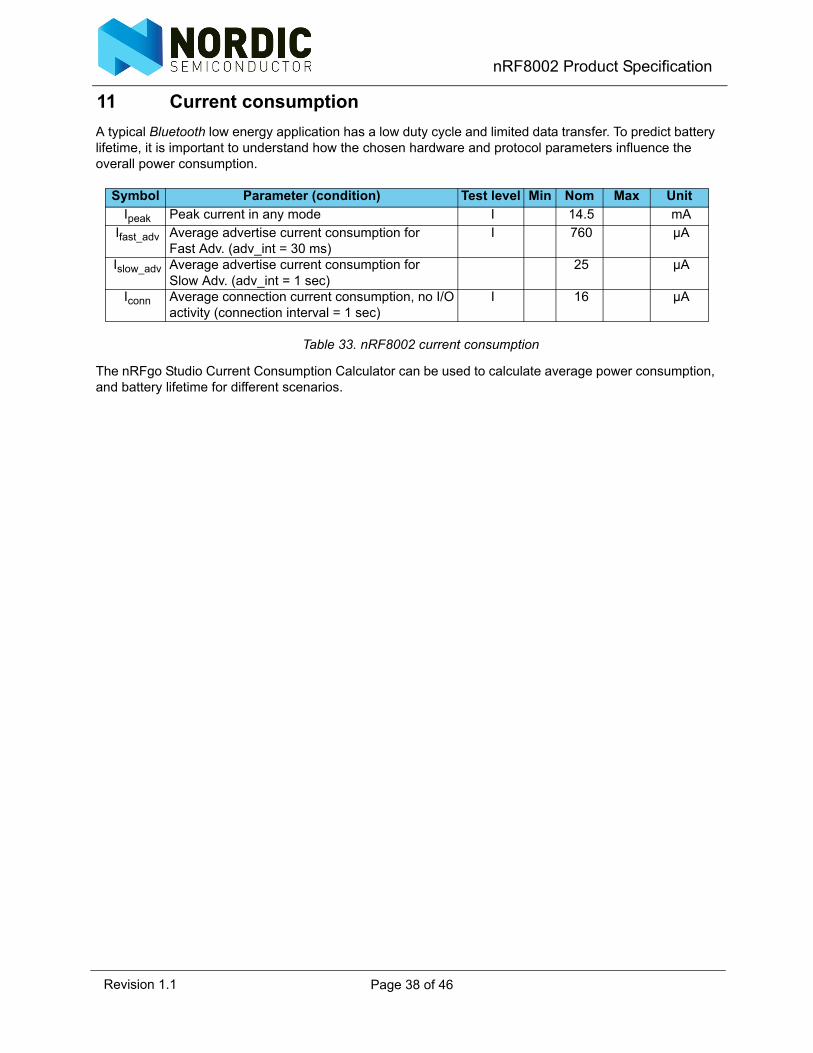
11 Current consumption
A typical Bluetooth low energy application has a low duty cycle and limited data transfer. To predict battery lifetime, it is important to understand how the chosen hardware and protocol parameters influence the overall power consumption.
Table 33. nRF8002 current consumption
The nRFgo Studio Current Consumption Calculator can be used to calculate average power consumption, and battery lifetime for different scenarios.
Symbol Parameter (condition) Test level Min Nom Max Unit
Ipeak Peak current in any mode I 14.5 mAIfast_adv Average advertise current consumption for
Fast Adv. (adv_int = 30 ms)I 760 µA
Islow_adv Average advertise current consumption for Slow Adv. (adv_int = 1 sec)
25 µA
Iconn Average connection current consumption, no I/O activity (connection interval = 1 sec)
I 16 µA
Page 38 of 46Revision 1.1

nRF8002 Product Specification
12 Hardware description
12.1 Reset
The RESET line should be held low for a minimum duration of 200 ns for the nRF8002 to reset.
12.2 16 MHz oscillator
The 16 MHz crystal oscillator is designed for use with an AT-cut quartz crystal in parallel resonant mode. To achieve correct oscillation frequency, the load capacitance must match the specification in the crystal data sheet. Figure 11. shows how the crystal is connected to the 16 MHz crystal oscillator.
Figure 11. Circuit diagram of nRF8002’s 16 MHz crystal oscillator
The load capacitance is the total capacitance seen by the crystal across its terminals and is given by:
C1 and C2 are ceramic SMD capacitors connected between XC1 and XC2 and ground. Cpcb1 and Cpcb2 are stray capacitances on the PCB. Cpin is the input capacitance on the XC1 and XC2 pins, typically 1 pF. C1 and C2 should be of the same value.
12.2.1 Internal 32.768 kHz RC oscillator
The internal 32.768 kHz RC oscillator which provides the protocol and application timing for the connection to the peer device is an internal oscillator. No external components or configuration is required.
C1 C2
16 MHz crystal
XC1 XC2
pinCpcbCCC
pinCpcbCCC
CC
CCloadC
_2_2'2
_1_1'1
)'2'1(
)'2'1(
Page 39 of 46Revision 1.1

nRF8002 Product Specification
12.3 UART interface characteristics
The UART interface used for device configuration and Direct Test Mode (DTM) operation has the following features:
• 2-wire UART interface (TXD/RXD)• Baud rate: 19200• 8 data bits• No parity• 1 stop bit• No flow control (meaning no RTS/CTS)
UART interface pins are described in Figure 2. on page 7 and Table 1. on page 8.
12.4 Antenna matching and balun
The ANT1 and ANT2 pins provide a balanced RF connection to the antenna. The pins must have a DC to VDD_PA, either through an RF choke or through the center point in a balanced dipole antenna. A load impedance at ANT1 and ANT2 of 15 Ω and j88 Ω is recommended for maximum output. A load impedance of 50 Ω can be obtained by fitting a simple matching network between the load and the ANT1 and ANT2 pins.
12.5 PCB layout and decoupling guidelines
A well designed PCB is necessary to achieve good RF performance. A poor layout can lead to loss of performance or functionality. A fully qualified RF-layout for the nRF8002 and its surrounding components, including matching networks, can be downloaded from www.nordicsemi.com.
A PCB with a minimum of two layers including a ground plane is recommended for optimum performance. The nRF8002 DC supply voltage should be decoupled as close as possible to the VDD pins with high performance RF capacitors.See the schematics layout in chapter 15 on page 43 for recommended decoupling capacitor values. The nRF8002 supply voltage should be filtered and routed separately from the supply voltages of any digital circuitry.
Long power supply lines on the PCB should be avoided. All device grounds, VDD connections and VDD bypass capacitors must be connected as close as possible to the nRF8002 IC. For a PCB with a topside RF ground plane, the VSS pins should be connected directly to the ground plane. For a PCB with a bottom ground plane, the best technique is to have via holes as close as possible to the VSS pads. A minimum of one via hole should be used for each VSS pin.
Full swing digital data or control signals should not be routed close to the crystal or the power supply lines.
Page 40 of 46Revision 1.1

nRF8002 Product Specification
13 Mechanical specifications
nRF8002 is packaged in a QFN32 5×5×0.85 mm, 0.5 mm pitch.
Table 34. QFN32 dimensions in mm
Package A A1 A3 b D, E D2, E2 e K L
QFN32 0.800.850.90
0.000.020.05
0.200.180.250.30
4.95.05.1
3.503.603.70
0.50.20 0.35
0.400.45
MinNomMax
D
A
D2
E2E
A1 A3SIDE VIEW
TOP VIEW
1
2
32 31
b
L
2
1
e
K
32 31
BOTTOM VIEW
Page 41 of 46Revision 1.1

nRF8002 Product Specification
14 Ordering information
14.1 Package marking
14.2 Abbreviations
Table 35. Abbreviations
14.3 Product options
14.3.1 RF silicon
Table 36. nRF8002 RF silicon options
14.3.2 Development tool
Table 37. nRF8002 solution option
N R F B X
8 0 0 2
Y Y W W L L
Abbreviation Definition
8002 Product numberB Build Code, that is, unique code for production sites, package type and test platformX "X" grade, that is, Engineering Samples (optional)
YY Two-digit year numberWW Two-digit week numberLL Two-letter wafer-lot number code
Ordering code Package Container MOQ1
1. Minimum Order Quantity
MSL2
2. Moisture Sensitivity Level
nRF8002-R1Q32-R 5x5 mm 32-pin QFN, lead free (green)
13” Reel 4000 2
nRF8002-R1Q32-R7 5x5 mm 32-pin QFN, lead free (green)
7” Reel 1500 2
nRF8002-R1Q32-T 5x5 mm 32-pin QFN, lead free (green)
Tray 490 2
Type Number Description
nRF8002-DK nRF8002 Development Kit
Page 42 of 46Revision 1.1

nRF8002 Product Specification
15 Example application circuitry
15.1 PCB guidelines
To ensure optimal performance it is essential that you follow the schematics- and layout references closely. Especially in the case of the antenna matching circuitry (components between device pins ANT1,ANT2, VDD_PA and the antenna), any changes to the layout can change the behavior, resulting in degradation of RF performance or a need to change component values. All the reference circuits are designed for use with a 50 ohm single end antenna. See Section 12.5 on page 40 for more information.
15.2 Schematic nRF8002 example application
Figure 12. Schematic nRF8002 example application
L18.2nH
L2
5.6nH
L3
3.9nH
C1
12pF
C2
12pF
C32.2nF
C4N.C.
C5
1.8pFC61.2pF
X1
16MHz
R1
22k
C81.0nF
VCC_nRF
C9100nF
VCC_nRF
VCC_nRF
RES
ET
C10100nF
C1133nF
C12100nF
VDD1
DEC12
VSS8 TXD7
RXD
10
DEC23
VSS4
IN1
11
IN2
12
PWM6
VSS
13
VDD
9
OUT1
14
OUT2
15
OUT3
16
VSS 17VSS 18
XC1
28AVDD
29
RESET 19VDD_PA 20ANT1 21ANT2 22VSS 23AVDD 24
IREF
25AVDD
26XC2
27
VSS
31
VSS
30
NC
32
nRF8002
VSS5
U1nRF8002
IN1
IN2
OUT2
OUT1
OUT3
RXD
TXD
PWM
Page 43 of 46Revision 1.1

nRF8002 Product Specification
15.3 PCB layout nRF8002 example application
Figure 13. PCB layout nRF8002 example application
Top view Bottom view
No componentsIn bottom layer
Top silk screen
Page 44 of 46Revision 1.1

nRF8002 Product Specification
15.4 Bill of Materials nRF8002 example application
Table 38. Bill of materials nRF8002 example application
Designator Value Footprint Comment
C1, C2 12 pF 0402 Capacitor, NP0 ± 2%
C3 2.2 nF 0402 Capacitor, X7R ± 10%
C4 NA 0402 Not mounted
C5 1.8 pF 0402 Capacitor, NP0 ± 0.1 pF
C6 1.2 pF 0402 Capacitor, NP0 ± 0.1 pF
C8 1.0 nF 0402 Capacitor, X7R ± 10%
C9, C10, C12 100 nF 0402 Capacitor, X7R ± 10%
C11 33 nF 0402 Capacitor, X7R ± 10%
L1 8.2 nH 0402 High frequency chip inductor ± 5%
L2 5.6 nH 0402 High frequency chip inductor ± 5%
L3 3.9 nH 0402 High frequency chip inductor ± 5%
R1 22 kΩ 0402 Resistor, ± 1%, 0.063 W
U1 nRF8002 QFN32 QFN32 5×5 mm package
X1 16 MHz 3.2 × 2.5 mm SMD-3225, 16 MHz, CL=9 pF, ± 40 ppm
PCB substrate FR4 laminate 2 layer, thickness 1.6 mm
Page 45 of 46Revision 1.1

nRF8002 Product Specification
16 Glossary
Term Description
ACI Application Controller InterfaceBTLE Bluetooth Low EnergyCCCD Client Characteristic Configuration DescriptorCSRK Connection Signature Resolving KeyDTM Direct Test ModeEDIV Encrypted DiversifierEOC Extreme Operating Conditions
EP-QDL End Product Qualified Design ListingESR Equivalent Series ResistanceGAP Generic Access ProfileGATT Generic Attribute Profile
HV Handle ValueIMD Intermodulation DistortionIRK Identity Root KeyLTK Long Term KeyMD More Data
MOQ Minimum Order QuantityMCU Micro Controller UnitMSC Message Sequence ChartMSL Moisture Sensitivity Level according to JEDEC classificationNOC Nominal Operating ConditionsNVM Non-Volatile MemoryOOR Out Of RangePCB Printed Circuit BoardPDU Protocol Data UnitPHY PhysicalPICS Protocol Implementation Conformance StatementPUID Personal User Interface DeviceRF Radio Frequency
RoHS Restriction of Hazardous Substances SDK Software Development Kit
UART Universal Asynchronous Receiver TransmitterVM Volatile Memory
Page 46 of 46Revision 1.1