programmable dual-axis inclinometer/accelerometer data ... · sensor data provides developers with...
TRANSCRIPT
Programmable Dual-Axis Inclinometer/Accelerometer
Data Sheet ADIS16201
Rev. E Document Feedback Information furnished by Analog Devices is believed to be accurate and reliable. However, no responsibility is assumed by Analog Devices for its use, nor for any infringements of patents or other rights of third parties that may result from its use. Specifications subject to change without notice. No license is granted by implication or otherwise under any patent or patent rights of Analog Devices. Trademarks and registered trademarks are the property of their respective owners.
One Technology Way, P.O. Box 9106, Norwood, MA 02062-9106, U.S.A. Tel: 781.329.4700 ©2006–2019 Analog Devices, Inc. All rights reserved. Technical Support www.analog.com
FEATURES Dual-axis inclinometer/accelerometer measurements 12-, 14-bit digital inclination/acceleration sensor outputs ±1.7 g accelerometer measurement range ±90° inclinometer measurement range, linear output 12-bit digital temperature sensor output Digitally controlled sensitivity and bias calibration Digitally controlled sample rate Digitally controlled frequency response Dual alarm settings with rate/threshold limits Auxiliary digital I/O Digitally activated self test Digitally activated low power mode SPI®-compatible serial interface Auxiliary 12-bit ADC input and DAC output Single-supply operation: 3.0 V to +3.6 V 3500 g powered shock survivability
APPLICATIONS Platform control, stabilization, and leveling Tilt sensing, inclinometers Motion/position measurement Monitor/alarm devices (security, medical, safety)
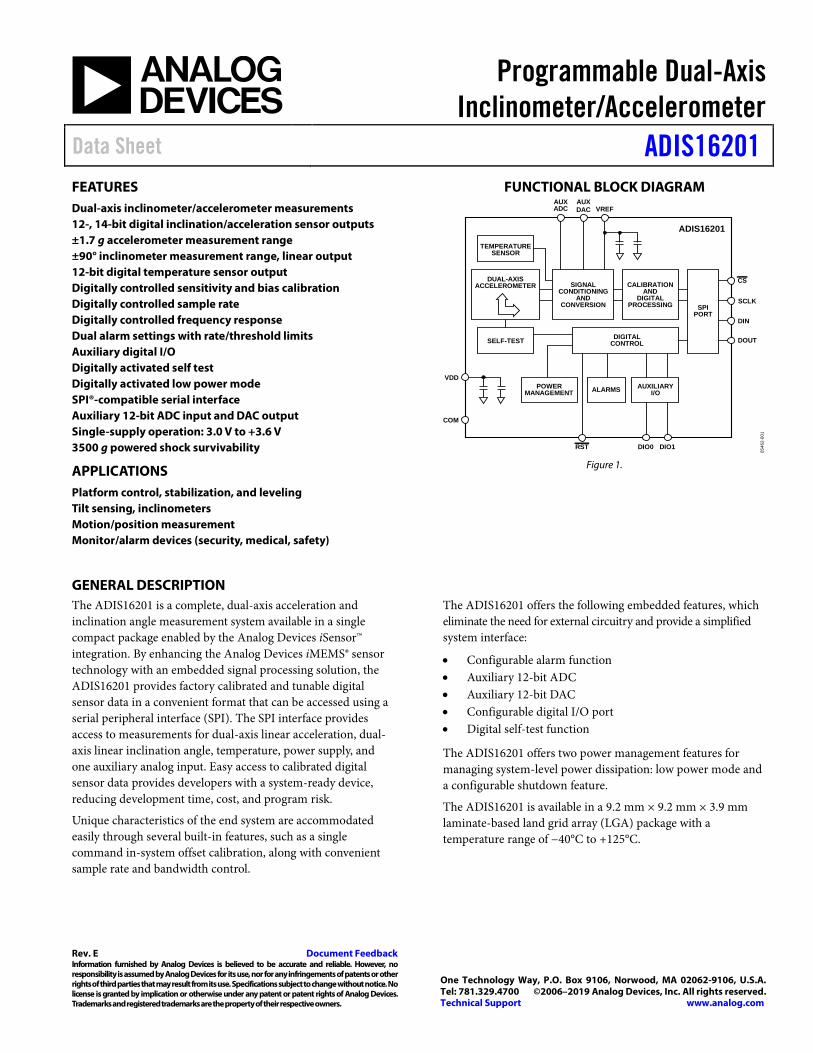
FUNCTIONAL BLOCK DIAGRAM
SCLK
DIN
DOUT
CS
RST DIO0 DIO1
SPIPORT
TEMPERATURESENSOR
SELF-TEST
POWERMANAGEMENT
AUXILIARYI/OALARMS
DIGITALCONTROL
SIGNALCONDITIONING
ANDCONVERSION
CALIBRATIONAND
DIGITALPROCESSING
ADIS16201
VDD
COM
AUXADC
AUXDAC VREF
DUAL-AXISACCELEROMETER
0546
2-00
1
Figure 1.
GENERAL DESCRIPTION The ADIS16201 is a complete, dual-axis acceleration and inclination angle measurement system available in a single compact package enabled by the Analog Devices iSensor™ integration. By enhancing the Analog Devices iMEMS® sensor technology with an embedded signal processing solution, the ADIS16201 provides factory calibrated and tunable digital sensor data in a convenient format that can be accessed using a serial peripheral interface (SPI). The SPI interface provides access to measurements for dual-axis linear acceleration, dual-axis linear inclination angle, temperature, power supply, and one auxiliary analog input. Easy access to calibrated digital sensor data provides developers with a system-ready device, reducing development time, cost, and program risk.
Unique characteristics of the end system are accommodated easily through several built-in features, such as a single command in-system offset calibration, along with convenient sample rate and bandwidth control.
The ADIS16201 offers the following embedded features, which eliminate the need for external circuitry and provide a simplified system interface:
• Configurable alarm function • Auxiliary 12-bit ADC • Auxiliary 12-bit DAC • Configurable digital I/O port • Digital self-test function
The ADIS16201 offers two power management features for managing system-level power dissipation: low power mode and a configurable shutdown feature.
The ADIS16201 is available in a 9.2 mm × 9.2 mm × 3.9 mm laminate-based land grid array (LGA) package with a temperature range of −40°C to +125°C.
ADIS16201 Data Sheet
Rev. E | Page 2 of 31
TABLE OF CONTENTS Features .............................................................................................. 1 Applications ....................................................................................... 1 Functional Block Diagram .............................................................. 1 General Description ......................................................................... 1 Revision History ............................................................................... 2 Specifications ..................................................................................... 3
Timing Specifications .................................................................. 5 Timing Diagrams .......................................................................... 5
Absolute Maximum Ratings ............................................................ 6 ESD Caution .................................................................................. 6
Pin Configuration and Function Descriptions ............................. 7 Typical Performance Characteristics ............................................. 8 Theory of Operation ...................................................................... 13
Accelerometer Operation .......................................................... 13 Inclinometer Operation ............................................................. 13 Temperature Sensor ................................................................... 13
Basic Operation............................................................................... 14 Data Output Register Access..................................................... 14
Programming and Control ............................................................ 16 Control Register Overview........................................................ 16 Control Register Access ............................................................. 16
Control Register Details................................................................. 18 Calibration ................................................................................... 18 Calibration Register Definitions ............................................... 18
Alarms .......................................................................................... 20 Sample Period Control .............................................................. 22 Filtering Control ......................................................................... 23 Power-Down Control ................................................................ 23 Status Feedback........................................................................... 24 Command Control ..................................................................... 24 Miscellaneous Control Register................................................ 25
Peripherals ....................................................................................... 26 Auxiliary ADC Function ........................................................... 26 Auxiliary DAC Function ........................................................... 26 General Purpose I/O Control ................................................... 27
Applications Information .............................................................. 28 Serial Peripheral Interface (SPI) ............................................... 28 Hardware Considerations ......................................................... 28 Grounding and Board Layout Recomendations .................... 28 Band Gap Reference ................................................................... 29 Power Supply Considerations ................................................... 29 Assembly ...................................................................................... 29 Example Pad Layout ................................................................... 29 X-Ray Sensitivity ........................................................................ 29
Outline Dimensions ....................................................................... 30 Ordering Guide .......................................................................... 30
REVISION HISTORY 3/2019—Rev. D to Rev. E Added Endnote 1 in Table 1 ............................................................ 3 Added X-Ray Sensitivity Section .................................................. 29 Changes to Ordering Guide .......................................................... 30 7/2018—Rev. C to Rev. D Changes to Inclinometer Operation Section .............................. 13 Deleted Figure 31 and Figure 32; Renumbered Sequentially ... 13 Deleted Figure 33 ............................................................................ 14 Changed Applications Section to Applications Information Section .............................................................................................. 28 Added Power Supply Considerations Section, Power-On-Reset Function Section, Transient Current from VDD Ramp Rate Section, and Assembly Section ..................................................... 29 Deleted Power-On Reset Operation Section, Figure 40, Second-Level Assembly Section, Figure 41, and Table 32; Renumbered Sequentially ..................................................................................... 30 Change to Ordering Guide ............................................................ 30
8/2013—Rev. B to Rev. C Changes to Endnote 5 and Added Endnote 6; Table 1 ................. 4 Changed Digital Input/Output Voltage to COM Parameter from −0.3 V to +5.5 V to −0.3 V to +5.3 V.............................................. 6 Changes to SMPL_PRD Register Definition Section, Table 24, and AVG_CNT Register Definition Section ............................... 24 Changes to Table 31 ....................................................................... 28 4/2013—Rev. A to Rev. B Changes to Table 2 ............................................................................. 5 Updated Outline Dimensions ....................................................... 31 Changes to Ordering Guide .......................................................... 31 5/2006—Rev. 0 to Rev. A Changes to Figure 3 ........................................................................... 5 Changes to Figure 35 ...................................................................... 18 Changes to Status Feedback Section ............................................ 25 3/2006—Revision 0: Initial Version
Data Sheet ADIS16201
Rev. E | Page 3 of 31
SPECIFICATIONS TA = −40oC to +125°C, VDD = 3.3 V, tilt = 0°, unless otherwise noted.
Table 1. Parameter Conditions Min Typ Max Unit INCLINOMETER Each axis
Input Range Operable to ~±90 degrees ±70 Degrees Relative Accuracy1 ±15 degrees, 25°C, max filter ±0.25 Degrees ±30 degrees, 25°C, max filter ±0.5 Degrees ±60 degrees, 25°C, max filter ±1.5 Degrees Sensitivity ±60 degrees, 25°C 9.9 10 10.1 LSB/degrees Sensitivity over Temperature ±30 degrees ±50 ppm/°C Offset1 At 25°C 2037 2048 2059 LSB Offset over Temperature ±0.082 LSB/°C
ACCELEROMETER Each axis Input Range2 At 25°C ±1.7 g Nonlinearity2 % of full scale ±0.5 ±2.5 % Alignment Error X sensor to Y sensor ±0.1 Degrees Cross Axis Sensitivity ±2 % Sensitivity At 25°C 2.140 2.162 2.184 LSB/mg Sensitivity over Temperature ±50 ppm/°C Offset At 25°C, 0 g 8151 8192 8233 LSB Offset over Temperature ±0.33 LSB/°C
ACCELEROMETER NOISE PERFORMANCE Output Noise At 25°C, no averaging 22 LSB rms Noise Density At 25°C, no averaging 0.37 LSB/√Hz rms
ACCELEROMETER FREQUENCY RESPONSE Sensor Bandwidth 2250 Hz Sensor Resonant Frequency 5.5 kHz
ACCELEROMETER SELF-TEST STATE3 Output Change When Active At 25°C 372 708 1040 LSB
TEMPERATURE SENSOR Output at 25°C 1278 LSB Scale Factor −2.13 LSB/°C
ADC INPUT Resolution 12 Bits Integral Nonlinearity ±2 LSB Differential Nonlinearity ±1 LSB Offset Error ±4 LSB Gain Error ±2 LSB Input Range 0 2.5 V Input Capacitance During acquisition 20 pF
ON-CHIP VOLTAGE REFERENCE 2.5 V Accuracy At 25°C −10 +10 mV Reference Temperature Coefficient ±40 ppm/°C Output Impedance 70 Ω
DAC OUTPUT 5 kΩ/100 pF to GND Resolution 12 Bits Relative Accuracy For Code 101 to Code 4095 4 LSB Differential Nonlinearity 1 LSB Offset Error ±5 mV Gain Error ±0.5 % Output Range 0 to 2.5 V
ADIS16201 Data Sheet
Rev. E | Page 4 of 31
Parameter Conditions Min Typ Max Unit Output Impedance 2 Ω Output Settling Time 10 μs
LOGIC INPUTS Input High Voltage, VINH 2.0 V Input Low Voltage, VINL 0.8 V Logic 1 Input Current, IINH VIH = VDD ±0.2 ±1 μA Logic 0 Input Current, IINL VIL = 0 V −40 −60 μA Input Capacitance, CIN 10 pF
DIGITAL OUTPUTS Output High Voltage, VOH ISOURCE = 1.6 mA 2.4 V Output Low Voltage, VOL ISINK = 1.6 mA 0.4 V
SLEEP TIMER Timeout Period4 0.5 128 Seconds
FLASH MEMORY Endurance5 20,000 Cycles Data Retention6 TJ = 85°C 20 Years
CONVERSION RATE Minimum Conversion Time 244 μs Maximum Conversion Time 484 ms Maximum Throughput Rate 4096 SPS Minimum Throughput Rate 2.066 SPS
POWER SUPPLY Operating Voltage Range VDD 3.0 3.3 3.6 V Power Supply Current Normal mode, SMPL_TIME ≥
0x08 (fS ≤ 910 Hz), at 25°C
11 14 mA
Fast mode, SMPL_TIME ≤ 0x07 (fS ≥ 1024 Hz), at 25°C
36 42 mA
Sleep mode, at 25°C 500 750 μA Turn-On Time7 130 ms
1 X-ray exposure may degrade this performance metric. 2 Guaranteed by iMEMs packaged part testing, design, and/or characterization. 3 Self-test response changes as the square of VDD. 4 Guaranteed by design. 5 Endurance is qualified as per JEDEC Standard 22 Method A117 and measured at −40°C, +25°C, +85°C, and +125°C. 6 Retention lifetime equivalent at junction temperature (TJ) 85°C as per JEDEC Standard 22 Method A117. Retention lifetime decreases with junction temperature. 7 The start-up time defines the time from VDD > 3.0 V to the first output register update. This parameter does not account for filter settling, which depends on the
SMPL_PRD and AVG_CNT settings.
Data Sheet ADIS16201
Rev. E | Page 5 of 31
TIMING SPECIFICATIONS TA = 25°C, VDD = 3.3 V, tilt = 0°, unless otherwise noted.
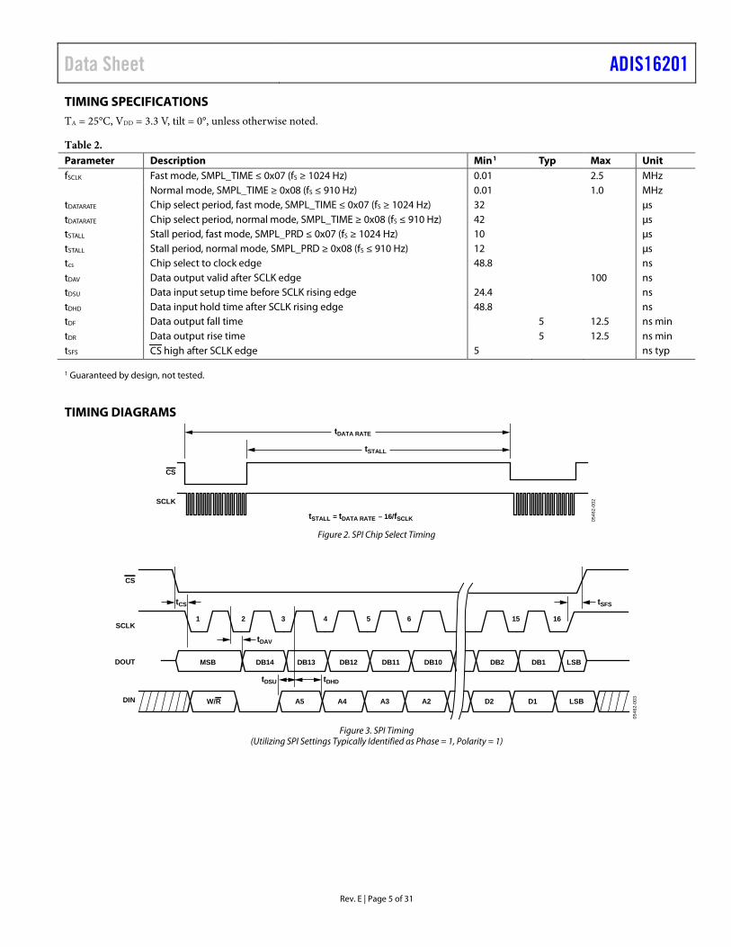
Table 2. Parameter Description Min1 Typ Max Unit fSCLK Fast mode, SMPL_TIME ≤ 0x07 (fS ≥ 1024 Hz) 0.01 2.5 MHz Normal mode, SMPL_TIME ≥ 0x08 (fS ≤ 910 Hz) 0.01 1.0 MHz tDATARATE Chip select period, fast mode, SMPL_TIME ≤ 0x07 (fS ≥ 1024 Hz) 32 μs tDATARATE Chip select period, normal mode, SMPL_TIME ≥ 0x08 (fS ≤ 910 Hz) 42 μs tSTALL Stall period, fast mode, SMPL_PRD ≤ 0x07 (fS ≥ 1024 Hz) 10 μs tSTALL Stall period, normal mode, SMPL_PRD ≥ 0x08 (fS ≤ 910 Hz) 12 μs tcs Chip select to clock edge 48.8 ns tDAV Data output valid after SCLK edge 100 ns tDSU Data input setup time before SCLK rising edge 24.4 ns tDHD Data input hold time after SCLK rising edge 48.8 ns tDF Data output fall time 5 12.5 ns min tDR Data output rise time 5 12.5 ns min tSFS CS high after SCLK edge 5 ns typ 1 Guaranteed by design, not tested.
TIMING DIAGRAMS
CS
SCLK
tDATA RATE
tSTALL = tDATA RATE – 16/fSCLK
tSTALL
0546
2-00
2
Figure 2. SPI Chip Select Timing
CS
SCLK
DOUT
DIN
1 2 3 4 5 6 15 16
W/R A5 A4 A3 A2 D2
MSB DB14
D1 LSB
DB13 DB12 DB10DB11 DB2 LSBDB1
tCS tSFS
tDAV
tDHDtDSU
0546
2-00
3
Figure 3. SPI Timing
(Utilizing SPI Settings Typically Identified as Phase = 1, Polarity = 1)
ADIS16201 Data Sheet
Rev. E | Page 6 of 31
ABSOLUTE MAXIMUM RATINGS Table 3. Parameter Rating Acceleration (Any Axis, Unpowered) 3500 g Acceleration (Any Axis, Powered) 3500 g VDD to COM −0.3 V to +7.0 V Digital Input/Output Voltage to COM −0.3 V to +5.3 V Analog Inputs to COM −0.3 to VDD + 0.3 V Analog Inputs to COM −0.3 to VDD + 0.3 V Operating Temperature Range −40°C to +125°C Storage Temperature Range −65°C to +150°C
Stresses at or above those listed under Absolute Maximum Ratings may cause permanent damage to the product. This is a stress rating only; functional operation of the product at these or any other conditions above those indicated in the operational section of this specification is not implied. Operation beyond the maximum operating conditions for extended periods may affect product reliability.
Table 4. Package Characteristics Package Type θJA θJC Device Weight 16-Terminal LGA 250°C/W 25°C/W 0.6 grams
ESD CAUTION
Data Sheet ADIS16201
Rev. E | Page 7 of 31
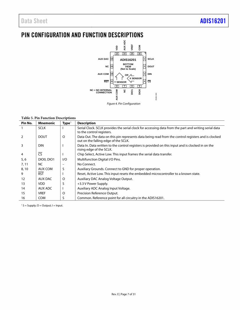
PIN CONFIGURATION AND FUNCTION DESCRIPTIONS
AUX
ADC
VDD
VREF
COM
NC
AUX
COM
DIO
1
DIO
0NC = NO INTERNAL CONNECTION
AUX DAC
NC
AUX COM
RST
SCLK
DOUT
DIN
X SENSORY SENSOR
OR
CS
ADIS16201BOTTOM
VIEW(Not to Scale)
1
2
3
12
9
10
11
4
5678
1613 14 15
0546
2-00
4
Figure 4. Pin Configuration
Table 5. Pin Function Descriptions Pin No. Mnemonic Type1 Description 1 SCLK I Serial Clock. SCLK provides the serial clock for accessing data from the part and writing serial data
to the control registers. 2 DOUT O Data Out. The data on this pin represents data being read from the control registers and is clocked
out on the falling edge of the SCLK. 3 DIN I Data In. Data written to the control registers is provided on this input and is clocked in on the
rising edge of the SCLK. 4 CS I Chip Select, Active Low. This input frames the serial data transfer.
5, 6 DIO0, DIO1 I/O Multifunction Digital I/O Pins. 7, 11 NC – No Connect. 8, 10 AUX COM S Auxiliary Grounds. Connect to GND for proper operation. 9 RST I Reset, Active Low. This input resets the embedded microcontroller to a known state.
12 AUX DAC O Auxiliary DAC Analog Voltage Output. 13 VDD S +3.3 V Power Supply. 14 AUX ADC I Auxiliary ADC Analog Input Voltage. 15 VREF O Precision Reference Output. 16 COM S Common. Reference point for all circuitry in the ADIS16201. 1 S = Supply; O = Output; I = Input.
ADIS16201 Data Sheet
Rev. E | Page 8 of 31
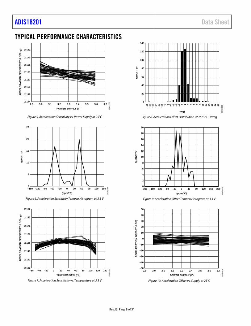
TYPICAL PERFORMANCE CHARACTERISTICS
2.1442.9 3.7
POWER SUPPLY (V)
ACCE
LERA
TIO
N SE
NSIT
IVIT
Y (L
SB/m
g) 2.174
2.170
2.165
2.161
2.157
2.153
2.148
3.0 3.1 3.2 3.3 3.4 3.5 3.6
0546
2-00
5
Figure 5. Acceleration Sensitivity vs. Power Supply at 25°C
25
0–150 150
(ppm/°C)
QUA
NTIT
Y
20
15
10
5
–120 –90 –60 –30 0 30 60 90 120
0546
2-00
6
Figure 6. Acceleration Sensitivity Tempco Histogram at 3.3 V
2.132–60 140
TEMPERATURE (°C)
ACC
ELER
ATIO
N SE
NSIT
IVIT
Y (L
SB/m
g)
2.192
2.183
2.175
2.166
2.158
2.149
2.141
–40 –20 0 20 40 60 80 100 120
0546
2-00
7
Figure 7. Acceleration Sensitivity vs. Temperature at 3.3 V
140
0
–18
–17
–15
–14
–12
–11 –9 –8 –6 –5 –3 –2 0 2 3 5 6 8 9 11 12 14 15 17 18
(mg)
QUA
NTIT
Y
120
100
80
60
40
20
0546
2-00
8
Figure 8. Acceleration Offset Distribution at 25°C/3.3 V/0 g
20
0–200 200
(ppm/°C)
QUA
NTIT
Y18
16
14
12
10
8
6
4
2
–160 –120 –80 –40 0 40 80 120 160
0546
2-00
9
Figure 9. Acceleration Offset Tempco Histogram at 3.3 V
50
–502.9 3.7
POWER SUPPLY (V)
ACCE
LERA
TIO
N O
FFSE
T (L
SB)
40
30
20
10
0
–10
–20
–30
–40
3.0 3.1 3.2 3.3 3.4 3.5 3.6
0546
2-01
0
Figure 10. Acceleration Offset vs. Supply at 25°C
Data Sheet ADIS16201
Rev. E | Page 9 of 31
90
0
0.18
0.19
0.20
0.21
0.22
0.23
0.24
0.25
0.26
0.27
0.28
0.29
0.30
0.31
0.32
0.33
0.34
0.35
0.36
0.37
0.38
0.39
0.40
0.41
0.42
(g)
QUA
NTIT
Y
80
70
60
50
40
30
20
10
0546
2-01
1
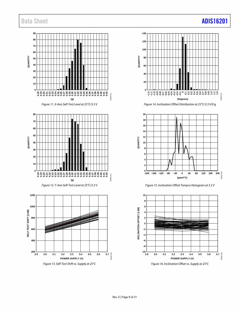
Figure 11. X-Axis Self-Test Level at 25°C/3.3 V
80
0
0.18
0.19
0.20
0.21
0.22
0.23
0.24
0.25
0.26
0.27
0.28
0.29
0.30
0.31
0.32
0.33
0.34
0.35
0.36
0.37
0.38
0.39
0.40
0.41
0.42
(g)
QUA
NTIT
Y
70
60
50
40
30
20
10
0546
2-01
2
Figure 12. Y-Axis Self-Test Level at 25°C/3.3 V
1200
2002.9 3.7
POWER SUPPLY (V)
SELF
-TES
T SH
IFT
(LSB
)
1000
800
600
400
3.0 3.1 3.2 3.3 3.4 3.5 3.6
0546
2-01
3
Figure 13. Self-Test Shift vs. Supply at 25°C
140
0
–1.2
–1.1
–1.0
–0.9
–0.8
–0.7
–0.6
–0.5
–0.4
–0.3
–0.2
–0.1 0
0.1
0.2
0.3
0.4
0.5
0.6
0.7
0.8
0.9
1.0
1.1
1.2
(Degrees)
QUA
NTIT
Y
120
100
80
60
40
20
0546
2-01
4
Figure 14. Inclination Offset Distribution at 25°C/3.3 V/0 g
20
0–200 200
(ppm/°C)
QUA
NTIT
Y
18
16
14
12
10
8
6
4
2
–160 –120 –80 –40 0 40 80 120 160
0546
2-01
5
Figure 15. Inclination Offset Tempco Histogram at 3.3 V
10
–102.9 3.7
POWER SUPPLY (V)
INCL
INAT
ION
OFF
SET
(LSB
)
3.0 3.1 3.2 3.3 3.4 3.5 3.6
8
6
4
2
0
–2
–4
–6
–8
0546
2-01
6
Figure 16. Inclination Offset vs. Supply at 25°C
ADIS16201 Data Sheet
Rev. E | Page 10 of 31
150
0
607.
660
7.8
608.
060
8.2
608.
460
8.6
608.
860
9.0
609.
260
9.4
609.
660
9.8
610.
061
0.2
610.
461
0.6
610.
861
1.0
611.
261
1.4
611.
661
1.8
612.
061
2.2
612.
4(µV/LSB)
QUA
NTIT
Y
125
100
75
50
25
0546
2-01
7
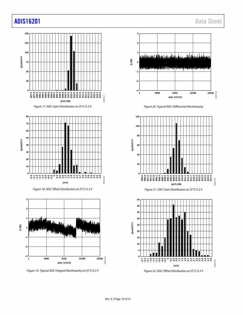
Figure 17. ADC Gain Distribution at 25°C/3.3 V
80
0
–2.4
–2.1
–1.8
–1.5
–1.2
–0.9
–0.6
–0.3 0
0.3
0.6
0.9
1.2
1.5
1.8
2.1
2.4
2.7
3.0
3.3
3.6
3.9
4.2
4.5
4.8
(mV)
QUA
NTIT
Y
70
60
50
40
30
20
10
0546
2-01
8
Figure 18. ADC Offset Distribution at 25°C/3.3 V
3
–31 16381
ADC STATE
(LSB
)
2
1
0
–1
–2
4096 8191 12286
0546
2-01
9
Figure 19. Typical ADC Integral Nonlinearity at 25°C/3.3 V
3
–31 16381
ADC STATE
(LSB
)
2
1
0
–1
–2
4096 8191 12286
0546
2-02
0
Figure 20. Typical ADC Differential Nonlinearity
120
0
606.
660
6.9
607.
260
7.5
607.
860
8.1
608.
460
8.7
609.
060
9.3
609.
660
9.9
610.
261
0.5
610.
861
1.1
611.
461
1.7
612.
061
2.3
612.
661
2.9
613.
261
3.5
617.
0
(µV/LSB)
QUA
NTIT
Y
100
80
60
40
20
0546
2-02
1
Figure 21. DAC Gain Distribution at 25°C/3.3 V
45
0
–2.7
–2.4
–2.1
–1.8
–1.5
–1.2
–0.9
–0.6
–0.3 0
0.3
0.6
0.9
1.2
1.5
1.8
2.1
2.4
2.7
3.0
3.3
3.6
3.9
4.2
4.8
(mV)
QUA
NTIT
Y
40
35
30
25
20
15
10
5
0546
2-02
2
Figure 22. DAC Offset Distribution at 25°C/3.3 V
Data Sheet ADIS16201
Rev. E | Page 11 of 31
5
–50 4096
DAC STATE
NONL
INEA
RITY
(LSB
)
4
3
2
1
0
–1
–2
–3
–4
512 1024 1536 2048 2560 3072 3584
3.0V/–40°C3.0V/+25°C3.0V/+125°C3.3V /–40°C3.3V/+25°C3.3V/+125°C3.6V/–40°C3.6V/+25°C3.6V/+125°C
0546
2-02
3
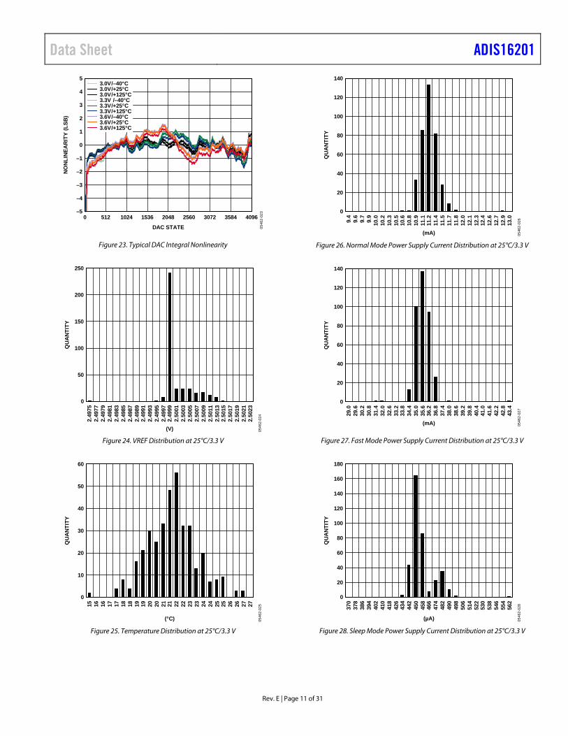
Figure 23. Typical DAC Integral Nonlinearity
250
0
2.49
752.
4977
2.49
792.
4981
2.49
832.
4985
2.49
872.
4989
2.49
912.
4993
2.49
952.
4997
2.49
992.
5001
2.50
032.
5005
2.50
072.
5009
2.50
112.
5013
2.50
152.
5017
2.50
192.
5021
2.50
23
(V)
QUA
NTIT
Y
200
150
100
50
0546
2-02
4
Figure 24. VREF Distribution at 25°C/3.3 V
60
0
15 16 16 17 17 18 18 19 19 20 20 21 21 22 22 23 23 24 24 25 25 26 26 27 27
(°C)
QUA
NTIT
Y
50
40
30
20
10
0546
2-02
5
Figure 25. Temperature Distribution at 25°C/3.3 V
140
0
9.4
9.6
9.7
9.9
10.0
10.2
10.3
10.5
10.6
10.8
10.9
11.1
11.2
11.4
11.5
11.7
11.8
12.0
12.1
12.3
12.4
12.6
12.7
12.9
13.0
(mA)
QUA
NTIT
Y
120
100
80
60
40
20
0546
2-02
6
Figure 26. Normal Mode Power Supply Current Distribution at 25°C/3.3 V
140
0
29.0
29.6
30.2
30.8
31.4
32.0
32.6
33.2
33.8
34.4
35.0
35.6
36.2
36.8
37.4
38.0
38.6
39.2
39.8
40.4
41.0
41.6
42.2
42.8
43.4
(mA)
QUA
NTIT
Y
120
100
80
60
40
20
0546
2-02
7
Figure 27. Fast Mode Power Supply Current Distribution at 25°C/3.3 V
180
0
370
378
386
394
402
410
418
426
434
442
450
458
466
474
482
490
498
506
514
522
530
538
546
554
562
(µA)
QUA
NTIT
Y
160
140
120
100
80
60
40
20
0546
2-02
8
Figure 28. Sleep Mode Power Supply Current Distribution at 25°C/3.3 V
ADIS16201 Data Sheet
Rev. E | Page 12 of 31
0–50 150
TEMPERATURE (°C)
SLEE
P M
ODE
CUR
RENT
(A)
0.0010
0.0008
0.0006
0.0004
0.0002
–30 –10 10 30 50 70 90 110 130
0546
2-02
9
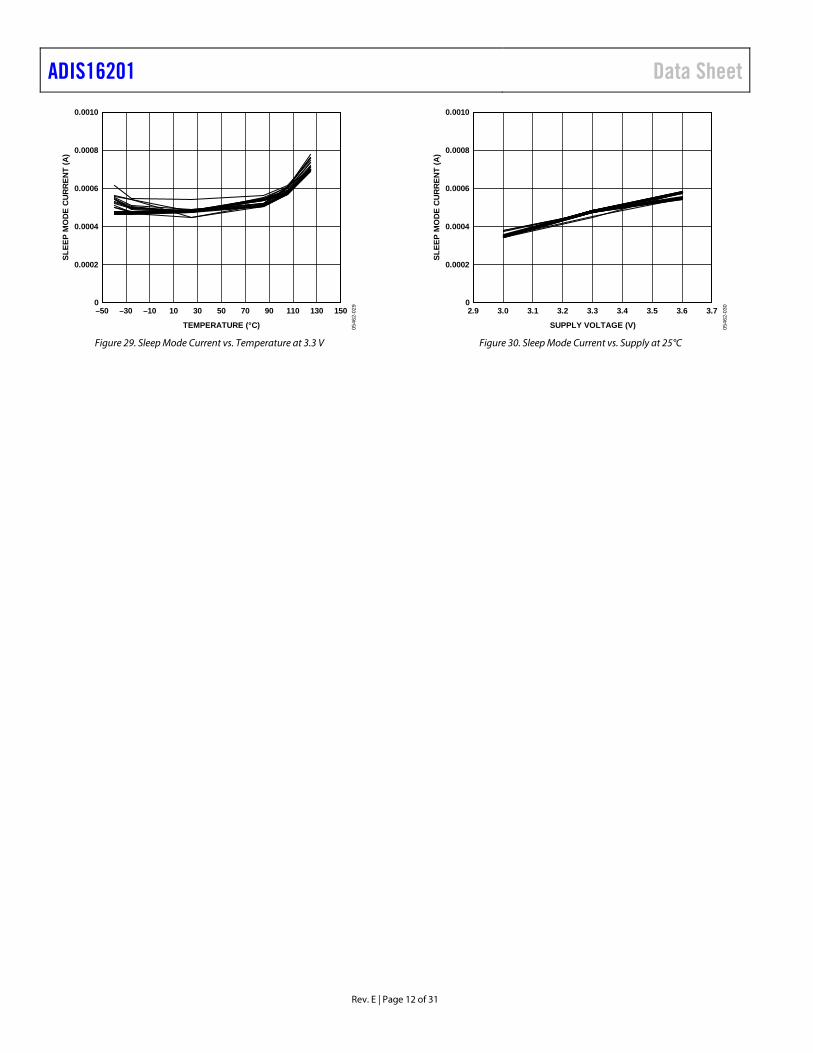
Figure 29. Sleep Mode Current vs. Temperature at 3.3 V
02.9 3.7
SUPPLY VOLTAGE (V)
SLEE
P M
ODE
CUR
RENT
(A)
0.0010
0.0008
0.0006
0.0004
0.0002
3.0 3.1 3.2 3.3 3.4 3.5 3.6
0546
2-03
0
Figure 30. Sleep Mode Current vs. Supply at 25°C
Data Sheet ADIS16201
Rev. E | Page 13 of 31
THEORY OF OPERATION The ADIS16201 is a complete dual-axis digital inclinometer/ accelerometer that uses Analog Devices’ surface-micromachining process and embedded signal processing to make a functionally complete, low cost dual-axis sensor.
The ADIS16201 offers a fully calibrated, dual–axis micromachined sensor element that develops independent analog signals representative of the acceleration levels applied to the part. An on-board precision ADC samples the acceleration signals, along with the power supply voltage, an internal temperature signal, and the auxiliary analog input signal. These signals are then processed and latched into addressable output registers. The serial peripheral interface (SPI) provides convenient, digital access to these registers.
In addition, the acceleration signals are further processed to produce inclination angle data for both axes. The inclination angle data represents the tilt away from the ideal plane, which in this case, is normal to the earth’s gravitational force. This calculation assumes that no force outside of the earth’s gravitational force is acting on the device.
ACCELEROMETER OPERATION The acceleration sensor used in the ADIS16201 is a surface-machined, polysilicon structure built on top of a silicon wafer. Polysilicon springs suspend the structure over the surface of the wafer and provide a resistance against acceleration forces. Acceleration causes a deflection in the differential capacitor structure that includes both fixed plates and plates that are attached to the moving mass. The fixed plates are driven by a set of square waves that are 180o out-of-phase from one another. Acceleration deflects the beam and unbalances the differential capacitor, resulting in an output square wave whose amplitude is proportional to acceleration. Phase sensitive demodulation
techniques rectify the signal and determine the direction of the acceleration. The output of the demodulator is amplified, digitized, and processed to remove any process variations and sensitivities to supply variations.
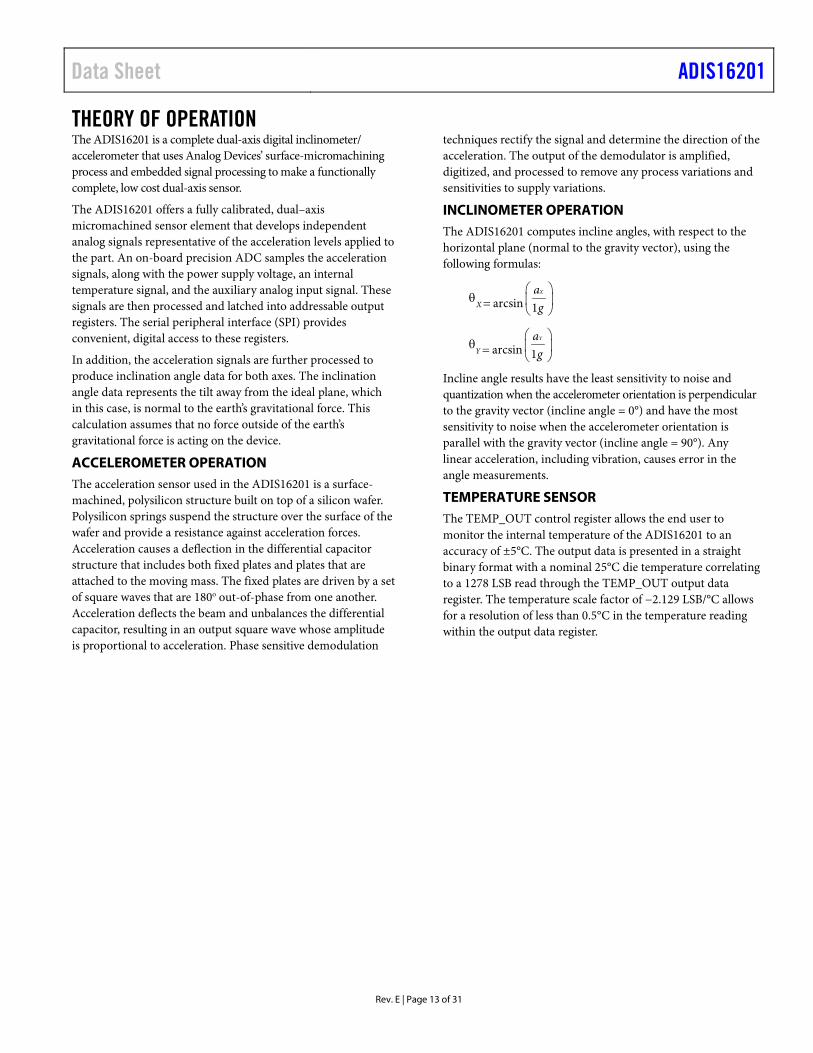
INCLINOMETER OPERATION The ADIS16201 computes incline angles, with respect to the horizontal plane (normal to the gravity vector), using the following formulas:
arcsin 1X
X
ag
θ =
arcsin 1Y
Y
ag
θ =
Incline angle results have the least sensitivity to noise and quantization when the accelerometer orientation is perpendicular to the gravity vector (incline angle = 0°) and have the most sensitivity to noise when the accelerometer orientation is parallel with the gravity vector (incline angle = 90°). Any linear acceleration, including vibration, causes error in the angle measurements.
TEMPERATURE SENSOR The TEMP_OUT control register allows the end user to monitor the internal temperature of the ADIS16201 to an accuracy of ±5°C. The output data is presented in a straight binary format with a nominal 25°C die temperature correlating to a 1278 LSB read through the TEMP_OUT output data register. The temperature scale factor of −2.129 LSB/°C allows for a resolution of less than 0.5°C in the temperature reading within the output data register.
ADIS16201 Data Sheet
Rev. E | Page 14 of 31
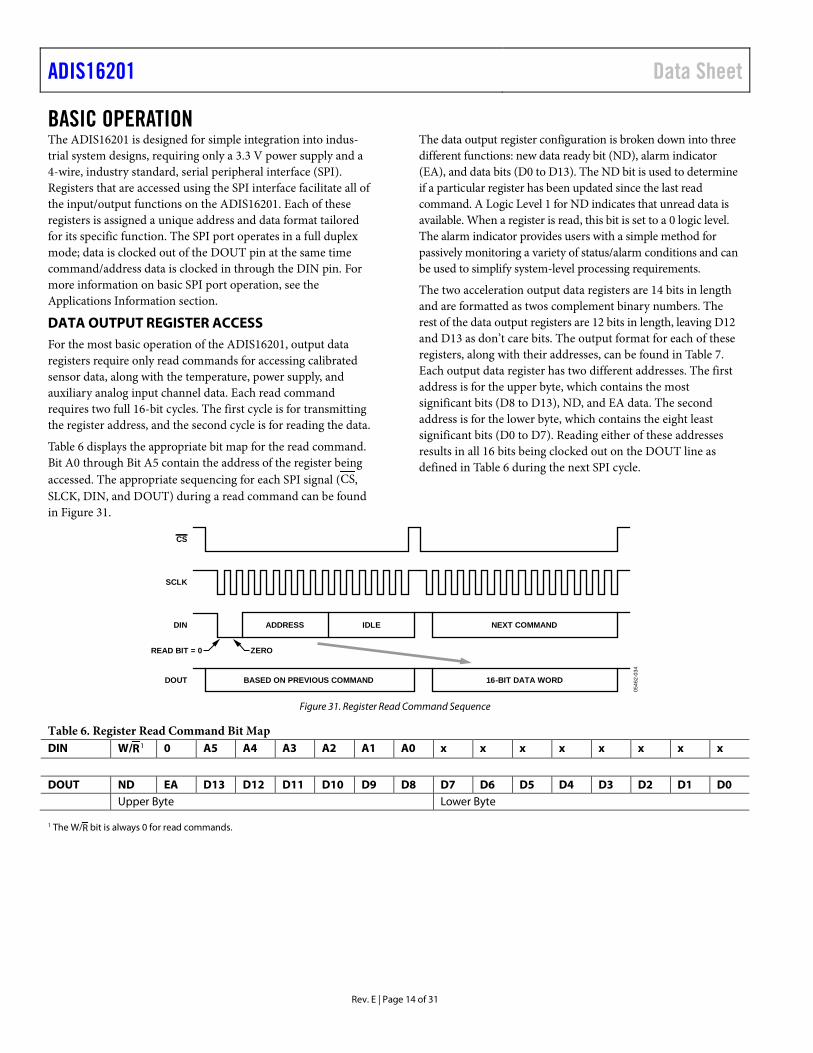
BASIC OPERATION The ADIS16201 is designed for simple integration into indus-trial system designs, requiring only a 3.3 V power supply and a 4-wire, industry standard, serial peripheral interface (SPI). Registers that are accessed using the SPI interface facilitate all of the input/output functions on the ADIS16201. Each of these registers is assigned a unique address and data format tailored for its specific function. The SPI port operates in a full duplex mode; data is clocked out of the DOUT pin at the same time command/address data is clocked in through the DIN pin. For more information on basic SPI port operation, see the Applications Information section.
DATA OUTPUT REGISTER ACCESS For the most basic operation of the ADIS16201, output data registers require only read commands for accessing calibrated sensor data, along with the temperature, power supply, and auxiliary analog input channel data. Each read command requires two full 16-bit cycles. The first cycle is for transmitting the register address, and the second cycle is for reading the data.
Table 6 displays the appropriate bit map for the read command. Bit A0 through Bit A5 contain the address of the register being accessed. The appropriate sequencing for each SPI signal (CS, SLCK, DIN, and DOUT) during a read command can be found in Figure 31.
The data output register configuration is broken down into three different functions: new data ready bit (ND), alarm indicator (EA), and data bits (D0 to D13). The ND bit is used to determine if a particular register has been updated since the last read command. A Logic Level 1 for ND indicates that unread data is available. When a register is read, this bit is set to a 0 logic level. The alarm indicator provides users with a simple method for passively monitoring a variety of status/alarm conditions and can be used to simplify system-level processing requirements.
The two acceleration output data registers are 14 bits in length and are formatted as twos complement binary numbers. The rest of the data output registers are 12 bits in length, leaving D12 and D13 as don’t care bits. The output format for each of these registers, along with their addresses, can be found in Table 7. Each output data register has two different addresses. The first address is for the upper byte, which contains the most significant bits (D8 to D13), ND, and EA data. The second address is for the lower byte, which contains the eight least significant bits (D0 to D7). Reading either of these addresses results in all 16 bits being clocked out on the DOUT line as defined in Table 6 during the next SPI cycle.
ADDRESS IDLE NEXT COMMAND
BASED ON PREVIOUS COMMAND 16-BIT DATA WORD
CS
SCLK
DIN
DOUT
READ BIT = 0 ZERO
0546
2-03
4
Figure 31. Register Read Command Sequence
Table 6. Register Read Command Bit Map DIN W/R1 0 A5 A4 A3 A2 A1 A0 x x x x x x x x
DOUT ND EA D13 D12 D11 D10 D9 D8 D7 D6 D5 D4 D3 D2 D1 D0 Upper Byte Lower Byte
1 The W/R bit is always 0 for read commands.
Data Sheet ADIS16201
Rev. E | Page 15 of 31
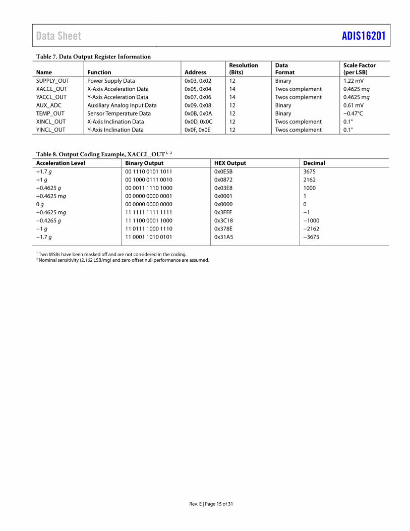
Table 7. Data Output Register Information
Name Function Address Resolution (Bits)
Data Format
Scale Factor (per LSB)
SUPPLY_OUT Power Supply Data 0x03, 0x02 12 Binary 1.22 mV XACCL_OUT X-Axis Acceleration Data 0x05, 0x04 14 Twos complement 0.4625 mg YACCL_OUT Y-Axis Acceleration Data 0x07, 0x06 14 Twos complement 0.4625 mg AUX_ADC Auxiliary Analog Input Data 0x09, 0x08 12 Binary 0.61 mV TEMP_OUT Sensor Temperature Data 0x0B, 0x0A 12 Binary −0.47°C XINCL_OUT X-Axis Inclination Data 0x0D, 0x0C 12 Twos complement 0.1° YINCL_OUT Y-Axis Inclination Data 0x0F, 0x0E 12 Twos complement 0.1°
Table 8. Output Coding Example, XACCL_OUT1, 2 Acceleration Level Binary Output HEX Output Decimal +1.7 g 00 1110 0101 1011 0x0E5B 3675 +1 g 00 1000 0111 0010 0x0872 2162 +0.4625 g 00 0011 1110 1000 0x03E8 1000 +0.4625 mg 00 0000 0000 0001 0x0001 1 0 g 00 0000 0000 0000 0x0000 0 −0.4625 mg 11 1111 1111 1111 0x3FFF −1 −0.4265 g 11 1100 0001 1000 0x3C18 −1000 −1 g 11 0111 1000 1110 0x378E −2162 −1.7 g 11 0001 1010 0101 0x31A5 −3675
1 Two MSBs have been masked off and are not considered in the coding. 2 Nominal sensitivity (2.162 LSB/mg) and zero offset null performance are assumed.
ADIS16201 Data Sheet
Rev. E | Page 16 of 31
PROGRAMMING AND CONTROL CONTROL REGISTER OVERVIEW The ADIS16201 offers many programmable features that are controlled by writing commands to the appropriate control registers using the SPI. For added system flexibility and programmability, the following sections describe these controls and specify the 28 digital control registers that are available using the SPI interface. A high level listing of these registers is given within Table 9. The following sections expand upon the functionality of each of these control registers, providing for the full clarification of the behavior of each of the control registers. Available control modes for the device include selectable sample rates for reading the seven output vectors, configurable output data, alarm settings, control of the on-board 12-bit auxiliary DAC, handling of the two general-purpose I/O lines, facilitation of the sleep mode, enabling the self-test mode, and other miscellaneous control functions.
The conversion process is repeated continually, providing for continuous update of the seven output registers. The new data ready bit (ND) flags bits common to all seven output registers, allowing the completion of the conversion process to be tracked via the SPI. As an alternative, the digital I/O lines can be configured through software control to create a data-ready hardware function that can signal the completion of the conversion process.
Two independent alarms provide the ability to monitor any one of the seven output registers. They can be configured to report an alarm condition on either fixed thresholds or rates of change. The alarm conditions are monitored through the SPI. In addition, the user can configure the digital I/O lines through software control to create an alarm function that allows for monitoring of the alarm conditions through hardware.
The seven output signals noted above are calibrated independ-ently at the factory, delivering a high degree of accuracy. In addition, the user has access to independent offset and scale factors for each of the two acceleration and inclination output vectors. This allows independent scaling and level adjustment control of any one these four registers prior to the values being read via the SPI. In turn, field level calibrations can be implemented within the sensor itself using these offset and scale variables. System level commands provided within the sensor include automatic zeroing of the four outputs using a single null command via the SPI. In addition, the original factory calibration settings can be recovered at any point, using a simple factory reset command.
CONTROL REGISTER ACCESS The control registers within the ADIS16201 are based upon a 16-bit/2-byte format, and they are accessed via the SPI. The SPI operates in full duplex mode with the data clocked out of the DOUT pin at the same time data is clocked in through the DIN pin. All commands written to the ASIS16201 are categorized as write commands or read commands. All write commands are self-contained and take place within a single cycle. Each read command requires two cycles to complete; the first cycle is for transmitting the register address, and the second cycle is for reading the data. During the second cycle, when the data out line is active, the data in line is used to receive the next sequential command. This allows for overlapping the commands. For more information on basic SPI port operation, see the Applications Information section.
The read and write commands are identified through the most significant bit (MSB), B15, of the received data. Write a 1 to B15 to indicate a write command. Write a 0 to B15 to indicate a read command. Bit B13 through Bit B8 contain the address of the control register that is being accessed. The remaining eight bits of the write command contain the data that is being written into the part, whereas the remaining eight bits of the read command contain don’t care levels. Given that the data within the write command is eight bits in length, the 8-bit data format is the default byte size. A write command operates on a single chip select cycle, as shown in Figure 32. The read command operates on a 2-chip select cycle basis, as seen in Figure 31. All 64 bytes of register space are accessed using the 6-bit address. Data written into the device is one byte at a time with the address of each byte being explicitly called out in the write command. Conversely, data being read from the device consists of two, back-to-back, 8-bit variables being sent out, with the first byte out corresponding to the upper address (odd number address) and the second byte relating to the next lower address space (even number address). For example, a data read of Address 03h results in the data from Address 03h being fed out followed by data from Address 02h. Likewise, a data read of Address 02h results in the same data stream being output from the device.
The ADIS16201 is a flash-based device with the nonvolatile functional registers implemented as flash registers. Take into account the endurance limitation of 20,000 writes when considering the system-level integration of these devices. The nonvolatile column in Table 9 indicates which registers are recovered upon power-up. The user must instigate a manual flash update command (using the command register) in order to store the nonvolatile data registers, once they are configured properly. When performing a manual flash update command, the user needs to ensure that the power supply remains within limits for a minimum of 50 μs after the write is initiated. This ensures a successful write of the nonvolatile data.
Data Sheet ADIS16201
Rev. E | Page 17 of 31
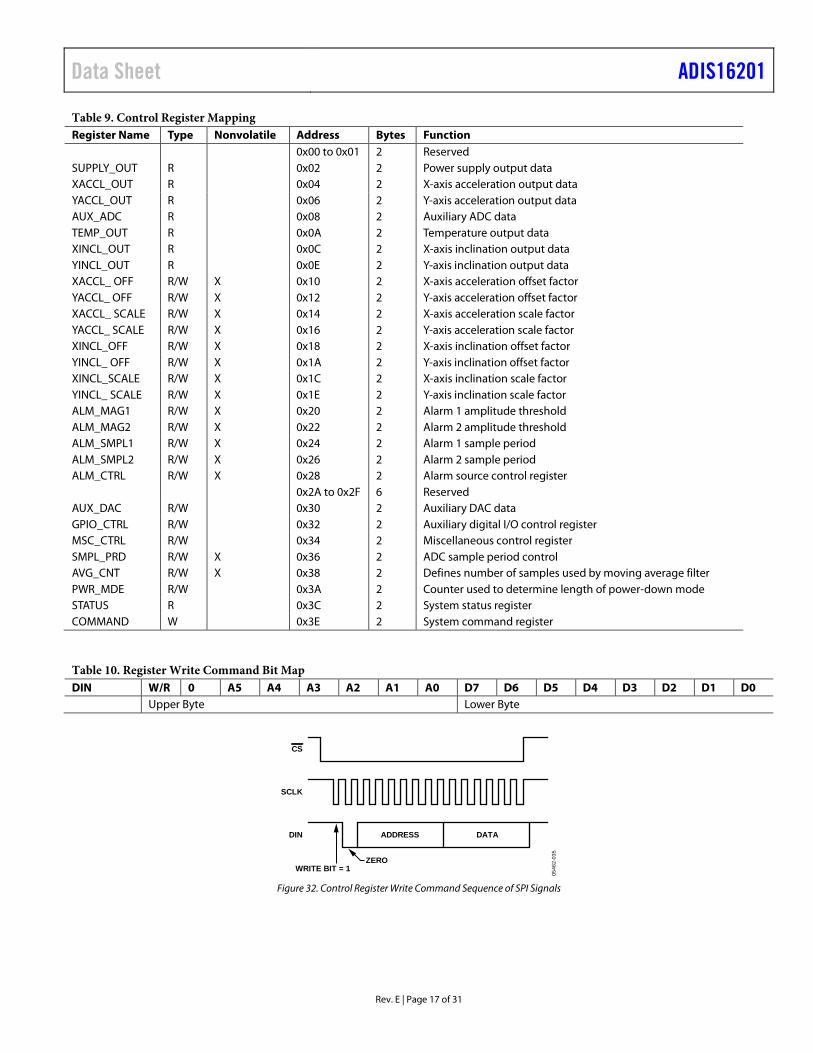
Table 9. Control Register Mapping Register Name Type Nonvolatile Address Bytes Function 0x00 to 0x01 2 Reserved SUPPLY_OUT R 0x02 2 Power supply output data XACCL_OUT R 0x04 2 X-axis acceleration output data YACCL_OUT R 0x06 2 Y-axis acceleration output data AUX_ADC R 0x08 2 Auxiliary ADC data TEMP_OUT R 0x0A 2 Temperature output data XINCL_OUT R 0x0C 2 X-axis inclination output data YINCL_OUT R 0x0E 2 Y-axis inclination output data XACCL_ OFF R/W X 0x10 2 X-axis acceleration offset factor YACCL_ OFF R/W X 0x12 2 Y-axis acceleration offset factor XACCL_ SCALE R/W X 0x14 2 X-axis acceleration scale factor YACCL_ SCALE R/W X 0x16 2 Y-axis acceleration scale factor XINCL_OFF R/W X 0x18 2 X-axis inclination offset factor YINCL_ OFF R/W X 0x1A 2 Y-axis inclination offset factor XINCL_SCALE R/W X 0x1C 2 X-axis inclination scale factor YINCL_ SCALE R/W X 0x1E 2 Y-axis inclination scale factor ALM_MAG1 R/W X 0x20 2 Alarm 1 amplitude threshold ALM_MAG2 R/W X 0x22 2 Alarm 2 amplitude threshold ALM_SMPL1 R/W X 0x24 2 Alarm 1 sample period ALM_SMPL2 R/W X 0x26 2 Alarm 2 sample period ALM_CTRL R/W X 0x28 2 Alarm source control register 0x2A to 0x2F 6 Reserved AUX_DAC R/W 0x30 2 Auxiliary DAC data GPIO_CTRL R/W 0x32 2 Auxiliary digital I/O control register MSC_CTRL R/W 0x34 2 Miscellaneous control register SMPL_PRD R/W X 0x36 2 ADC sample period control AVG_CNT R/W X 0x38 2 Defines number of samples used by moving average filter PWR_MDE R/W 0x3A 2 Counter used to determine length of power-down mode STATUS R 0x3C 2 System status register COMMAND W 0x3E 2 System command register
Table 10. Register Write Command Bit Map DIN W/R 0 A5 A4 A3 A2 A1 A0 D7 D6 D5 D4 D3 D2 D1 D0 Upper Byte Lower Byte
ADDRESS DATA
CS
SCLK
DIN
WRITE BIT = 1ZERO
0546
2-03
5
Figure 32. Control Register Write Command Sequence of SPI Signals
ADIS16201 Data Sheet
Rev. E | Page 18 of 31
CONTROL REGISTER DETAILS The control registers in the ADIS16201 are 16 bits in length. Each of them has been assigned an address for their upper byte and lower byte. The bit map of each control register uses the numerical assignments that are displayed in the following table.
MSB LSB
15 14 13 12 11 10 9 8
7 6 5 4 3 2 1 0
The upper byte consists of Bit 8 to Bit 15, and the lower byte consists of Bit 0 to Bit 7. Each of the following sections provides a description of each register that includes purpose, relevant scaling information, bit maps, addresses, and default values.
CALIBRATION The ADIS16201 outputs are precalibrated at the factory, providing a high degree of accuracy and simpler system implementation. In addition, for system or field updates, the device has eight control registers associated with calibrating the acceleration and inclination output data (see the Calibration Register Definitions section). Each of these registers has read/write capability and is 16 bits (2 bytes) in length. All calibration registers are 12 bits in length, with the exception of the inclination offset registers, which are 9 bits in length. All data values are aligned to the LSB. The OFFSET registers all utilize the twos complement format allowing for both positive and negative offsets. All scale registers utilize the straight binary format.
The data within these eight calibration registers is utilized in offsetting and scaling of the output data registers according to the following relationship:
CxAOutput
where: x represents the raw data prior to calibration. C is the offset. A is the scalar. Output represents the output data register where the resultant data is stored.
All four inertial sensor outputs (X and Y acceleration, X and Y inclination) have their own independent set of calibration registers.
Simple access to these registers enables field calibration to correct for in-system error sources. In particular, the offset control registers allow the user to reset to 0°/0 mg reference point for the device. This is particularly important when considering the stack-up of the tolerances in mounting the ADIS16201 to a printed circuit board (PCB), the PCB to an enclosure, the enclosure mounted to the chassis of a piece of equipment, and so on.
The result is that the ADIS16201 mechanical reference can be offset several degrees from that of the end equipment mechanical reference, resulting in an accumulation of offset errors in the inclination and acceleration data output registers. The offset registers provide a convenient tool for managing these types of errors.
A global command is implemented within the ADIS16201 to simplify the loading of the offsets. Once the end piece of equipment is leveled to its desired reference point, a null command can be sent to the ADIS16201 via the command control register, which zeros the two acceleration and the two inclination output data registers. This command loads all four offset registers with the inverse of their contents at the time of the null command. Consequently, on the next reading of the seven output data registers, the two acceleration and two inclination output data registers should be reset to mid-scale (neglecting noise and repeatability limitations). It is suggested that when the null command is implemented, the AVG_CNT control register be set to 08h in order to maximize the filtering and reduce the effects of noise in determining the values to be loaded into the offset control registers. Optionally, the user can manually load each of the eight calibration registers via the SPI in order to calibrate the end system. This is applicable when the user plans to adjust the scale factors, thus requiring an external stimulus to excite the ADIS16201.
CALIBRATION REGISTER DEFINITIONS XACCL_OFF Register Definition Address Scale1 Default Format Access 0x11, 0x10 0.4624 mg 0x0000 Twos
complement R/W
1 Scale is the weight of each LSB.
The XACCL_OFF register is the user-controlled register for calibrating system-level acceleration offset errors. For the X-axis acceleration, it represents the C variable in the calibration equation. The maximum calibration range is ±0.945 g, or +2047/−2048 codes, assuming nominal sensor sensitivity. The contents of this register are nonvolatile.
Table 11. XACCL_OFF Bit Designations Bit Description 15:12 Not used 11:0 Data bits
Data Sheet ADIS16201
Rev. E | Page 19 of 31
XACCL_SCALE Register Definition Address Scale1 Default Format Access 0x15, 0x14 0.0488% 0x0800 Binary R/W 1 Scale is the weight of each LSB.
The XACCL_SCALE register is the user-controlled register for calibrating system-level acceleration sensitivity errors. For the X-axis acceleration, it represents the A variable in the calibration equation. This register offers a sensitivity calibration range of 0 to 2, or 0 to 4095 codes, assuming nominal sensor sensitivity. The contents of this register are nonvolatile.
Table 12. XACCL_SCALE Bit Designations Bit Description 15:12 Not used 11:0 Data bits
YACCL_OFF Register Definition Address Scale1 Default Format R/W 0x13, 0x12 0.4624 mg 0x0000 Twos
complement Both
1 Scale is the weight of each LSB.
The YACCL_OFF register is the user-controlled register for calibrating system-level acceleration offset errors. For the Y-axis acceleration, it represents the C variable in the calibration equation. The maximum calibration range is ±0.945 g, or +2047/−2048 codes, assuming nominal sensor sensitivity. The contents of this register are nonvolatile.
Table 13. YACCL_OFF Bit Designations Bit Description 15:12 Not used 11:0 Data bits
YACCL_SCALE Register Definition Address Scale1 Default Format Access 0x17, 0x16 0.0488% 0x0800 Binary R/W 1 Scale is the weight of each LSB.
The YACCL_SCALE register is the user-controlled register for calibrating system-level acceleration sensitivity errors. For the Y-axis acceleration, it represents the A variable in the calibration equation. This register offers a sensitivity calibration range of 0 to 2, or 0 to 4095 codes, assuming nominal sensor sensitivity. The contents of this register are nonvolatile.
Table 14. YACCL_SCALE Bit Designations Bit Description 15:12 Not used 11:0 Data bits
XINCL_OFF Register Definition Address Scale1 Default Format Access 0x19, 0x18 0.1° 0x0000 Twos
complement R/W
1 Scale is the weight of each LSB.
The XINCL_OFF register is the user-controlled register for calibrating system-level inclination offset errors. For the X-axis inclination, it represents the C variable in the calibration equation. The maximum calibration range is ±25.5° or +255/−256 codes, assuming nominal sensor sensitivity. The contents of this register are nonvolatile.
Table 15. XINCL_OFF Bit Designations Bit Description 15:9 Not used 8:0 Data bits
XINCL_SCALE Register Definition Address Scale1 Default Format Access 0x1D, 0x1C 0.0488% 0x0800 Binary R/W 1 Scale is the weight of each LSB.
The XINCL_SCALE register is the user-controlled register for calibrating system-level inclination sensitivity errors. For the X-axis inclination, it represents the A variable in the calibration equation. The calibration range is from 0 to 2, or 0 to 4095 codes, assuming nominal sensor sensitivity. The contents of this register are nonvolatile.
Table 16. XINCL_SCALE Bit Designations Bit Description 15:12 Not used 11:0 Data bits
YINCL_OFF Register Definition Address Scale1 Default Format Access 0x1B, 0x1A 0.1º 0x0000 Twos
complement R/W
1 Scale is the weight of each LSB.
The YINCL_OFF register is the user-controlled register for calibrating system-level inclination offset errors. For the Y-axis inclination, it represents the C variable in the calibration equation. The maximum calibration range is ±25.5º or +255/ −256 codes, assuming nominal sensor sensitivity. The contents of this register are nonvolatile.
Table 17. YINCL_OFF Bit Designations Bit Description 15:9 Not used 8:0 Data bits
ADIS16201 Data Sheet
Rev. E | Page 20 of 31
YINCL_SCALE Register Definition Address Scale1 Default Format Access 0x1F, 0x1E 0.0488% 0x0800 Binary R/W 1 Scale is the weight of each LSB.
The YINCL_SCALE register is the user-controlled register for calibrating system-level inclination sensitivity errors. For the Y-axis inclination, it represents the A variable in the calibration equation. The calibration range is from 0 to 2, or 0 to 4095 codes, assuming nominal sensor sensitivity. The contents of this register are nonvolatile.
Table 18. YINCL_SCALE Bit Designations Bit Description 15:12 Not used 11:0 Data bits
ALARMS The ADIS16201 contains two independent alarm functions that are referred to as Alarm 1 and Alarm 2. The Alarm 1 function is managed by the ALM_MAG1 and ALM_SMPL1 control registers. The Alarm 2 function is managed by the ALM_MAG2 and ALM_SMPL2 control registers. Both the Alarm 1 and Alarm 2 functions share the ALM_CTRL register. For simplicity, the following text references the Alarm 1 functionality only.
The 16-bit ALM_CTRL register serves three distinct roles in controlling the Alarm 1 function. First, it is used to enable the overall Alarm 1 function and select the output data variable that is to be monitored for the alarm condition. Second, it is used to select whether the Alarm 1 function is based upon a predefined threshold (THR) level or a predefined rate-of-change (ROC) slope. Third, the ALM_CTRL register can be used in setting up one of the two general-purpose input/output lines (GPIOs) to serve as a hardware output that indicates when an alarm condition has occurred. Enabling the I/O alarm function, setting its polarity, and controlling its operation are accomplished using this register.
Note that when enabled, the hardware output indicator serves both the Alarm 1 and Alarm 2 functions and cannot be used to differentiate between one alarm condition and the other. It is simply used to indicate that an alarm is active and that the user should poll the device via the SPI to determine the source of the alarm condition (see the STATUS Register Definition section).
Because the ALM_CTRL, MSC_CTRL, and GPIO_CTRL control registers can influence the same GPIO pins, a priority level has been established to avoid conflicting assignments of the two GPIO pins. This priority level is defined as MSC_CTRL, which has precedence over ALM_CTRL, which has precedence over GPIO_CTRL.
The ALM_MAG1 control register used in controlling the Alarm 1 function has two roles. The first role is to store the value with which the output data variable is compared to discern if an alarm condition exists or not. The second role is to identify whether the alarm should be active for excursions above or below the alarm limit. If 1 is written to the GT1 bit of the ALM_MAG1 control register, the alarm is active for excursions extending above a given limit. If 0 is written to the GT1 bit, the alarm is active for excursions dropping below the given limit. The comparison value contained within the ALM_MAG1 control register is located within the lower 14 bits.
The format utilized for this 14-bit value should match that of the output data register that is being monitored for the alarm condition. For instance, if the YINCL_OUT output data register is being monitored by Alarm 1, then the 14-bit value within the ALM_MAG1 control register takes on a twos complement format with each LSB equating to nominal 0.1° (assumes unity scale and zero offset factors). The ALM_MAG value is compared against the instantaneous value of the parameter being monitored.
Use caution when monitoring the temperature output register for the alarm conditions. Here, the negative temperature scale factor results in the greater than and less than selections requiring reverse logic.
When the THR function is enabled, the output data variable is compared against the ALM_MAG1 level. When the ROC function is enabled, the comparison of the output data variable is against the ALM_MAG1 level averaged over the number of samples, as identified in the ALM_SMPL1 control register. This acts to create a comparison of (Δ units/Δ time) or the derivative of the output data variable against a predefined slope.
Data Sheet ADIS16201
Rev. E | Page 21 of 31
The versatility built into the alarm function is intended to allow the user to adapt to a number of different applications. For example, in the case of monitoring a twos complement variable, the GT1 bit within the ALM_MAG1 control register can allow for the detection of negative excursions below a fixed level. In addition, the Alarm 1 and Alarm 2 functions can be set to monitor the same variable that allows the user to discern if an output variable remains within a predefined window.
Other options include the ROC function that can be used in monitoring high frequency shock levels in the acceleration outputs or slowly changing outputs in the inclination level over a period of a minute or more. With the addition of the alarm hardware functionality, the ADIS16201 can be left to run independently of the main processor and interrupt the system only when an alarm condition occurs. Conversely, the alarm condition can be monitored through the routine polling of any one of the seven data output registers.
Note that the alarm functions work from instantaneous data and not averaged data that can be present when the AVG_CNT register is not set to 0. The alarm hardware output indicator is not latched but tracks the actual alarm conditions in real time.
ALM_MAG1 Register Definition Address Default1 Format Access 0x21, 0x20 0x0000 Not applicable R/W 1 Default is valid only until the first register write cycle.
The ALM_MAG1 register contains the threshold level for Alarm 1. The contents of this register are nonvolatile.
Table 19. ALM_MAG1 Bit Designations Bit Description 15 Greater than active alarm bit.
1: Alarm is active for an output greater than Alarm Magnitude 1 register setting. 0: Alarm is active for an output less than Alarm Magnitude 1 register setting.
14 Not used. 13:0 Data bits. This number can be either twos
complement or straight binary. The format is set by the value being monitored by this function.
ALM_SMPL1 Register Definition Address Default1 Format Access 0x25, 0x24 0x0000 Binary R/W 1 Default is valid only until the first register write cycle.
The ALM_SMPL1 register contains the sample period information for Alarm 1, when it is set for rate-of-change alarm monitoring. The rate-of-change alarm function averages the change in the output variable over the specified number of samples and compares this change directly to the values specified in the ALM_MAG1 register. The contents of this register are nonvolatile.
Table 20. ALM_SMPL1 Bit Designations Bit Description 15:8 Not used 7:0 Data bits
ALM_MAG2 Register Definition Address Default1 Format Access 0x23, 0x22 0x0000 Not applicable R/W 1 Default is valid only until the first register write cycle.
The ALM_MAG2 register contains the threshold level for Alarm 2. The contents of this register are nonvolatile.
Table 21. ALM_MAG2 Bit Designations Bit Description 15 Greater than active alarm bit.
1: Alarm is active for an output greater than Alarm Magnitude 2 register setting. 0: Alarm is active for an output less than Alarm Magnitude 2 register setting.
14 Not used. 13:0 Data bits. This number can be either twos
complement or straight binary. The format is set by the value being monitored by this function.
ALM_SMPL2 Register Definition Address Default1 Format Access 0x27, 0x26 0x0000 Binary R/W 1 Default is valid only until the first register write cycle.
The ALM_SMPL2 register contains the sample period information for Alarm 2, when it is set for rate-of-change alarm monitoring. The rate-of-change alarm function averages the change in the output variable over the specified number of samples and compares this change directly to the values specified in the ALM_MAG1 register. The contents of this register are nonvolatile.
Table 22. ALM_SMPL2 Bit Designations Bit Description 15:8 Not used 7:0 Data bits
ADIS16201 Data Sheet
Rev. E | Page 22 of 31
ALM_CTRL Register Definition Address Default1 Format Access 0x29, 0x28 0x0000 Not applicable R/W 1 Default is valid only until the first register write cycle.
The ALM_CTRL register contains the alarm control variables.
Table 23. ALM_CTRL Bit Designations Bit Value Description 15 Rate of change (ROC) enable for Alarm 2.
1: ROC is active. 0: ROC is inactive.
14:12 Alarm 2 source selection. 000 Alarm disable. 001 Alarm source: power supply output. 010 Alarm source: X-acceleration output. 011 Alarm source: Y-acceleration output. 100 Alarm source: auxiliary ADC output. 101 Alarm source: temperature sensor output. 110 Alarm source: X-inclination output. 111 Alarm source: Y-inclination output. 11 Rate of change (ROC) enable for Alarm 1.
1: ROC is active. 0: ROC is inactive.
10:8 Alarm 1 source selection. 000 Alarm disable. 001 Alarm source: power supply output. 010 Alarm source: X-acceleration output. 011 Alarm source: Y-acceleration output. 100 Alarm source: auxiliary ADC output. 101 Alarm source: temperature sensor output. 110 Alarm source: X-inclination output. 111 Alarm source: Y-inclination output. 7:3 Not used. 2 Alarm output enable.
1: Alarm output enabled. 0: Alarm output disabled.
1 Alarm output polarity. 1: Active high. 0: Active low.
0 Alarm output line select. 1: DIO1. 0: DIO0.
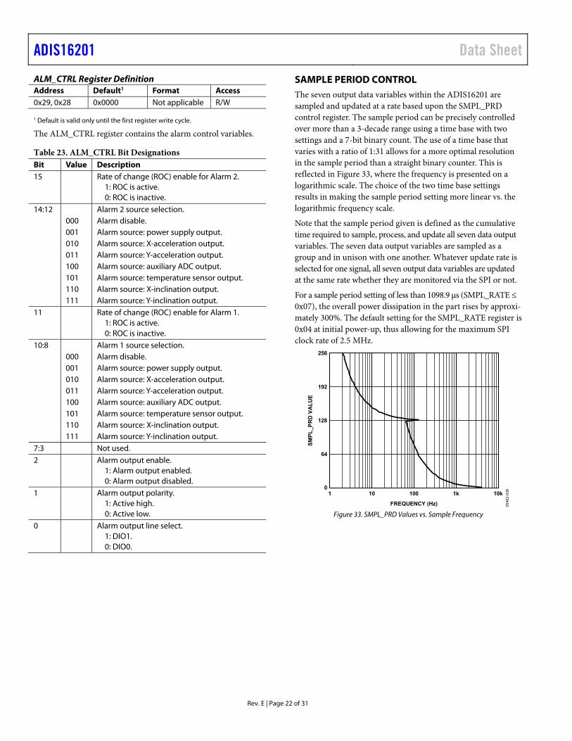
SAMPLE PERIOD CONTROL The seven output data variables within the ADIS16201 are sampled and updated at a rate based upon the SMPL_PRD control register. The sample period can be precisely controlled over more than a 3-decade range using a time base with two settings and a 7-bit binary count. The use of a time base that varies with a ratio of 1:31 allows for a more optimal resolution in the sample period than a straight binary counter. This is reflected in Figure 33, where the frequency is presented on a logarithmic scale. The choice of the two time base settings results in making the sample period setting more linear vs. the logarithmic frequency scale.
Note that the sample period given is defined as the cumulative time required to sample, process, and update all seven data output variables. The seven data output variables are sampled as a group and in unison with one another. Whatever update rate is selected for one signal, all seven output data variables are updated at the same rate whether they are monitored via the SPI or not.
For a sample period setting of less than 1098.9 μs (SMPL_RATE ≤ 0x07), the overall power dissipation in the part rises by approxi-mately 300%. The default setting for the SMPL_RATE register is 0x04 at initial power-up, thus allowing for the maximum SPI clock rate of 2.5 MHz.
256
01 10k
FREQUENCY (Hz)
SM
PL
_PR
D V
AL
UE
192
128
64
10 100 1k
05462-036
Figure 33. SMPL_PRD Values vs. Sample Frequency
Data Sheet ADIS16201
Rev. E | Page 23 of 31
SMPL_PRD Register Definition Address Default1 Format Access 0x37, 0x36 0x000A Not applicable R/W 1 Default is valid only until the first register write cycle.
After using the manual flash update (COMMAND[3]), the data within this register is nonvolatile, allowing for data recovery upon reset. The initial value is set to 0x0A upon initial power-up, allowing for a sample period of ~744 μs.
Table 24. SMPL_PRD Bit Descriptions Bit Description 15:8 Not used. 7 ADC time base control.
0: tB = 122.1 μs 1: tB = 3.784 ms .
6:0 ADC sample period control (NS). Relationship to the sample period control:
tS = tB × (NS + 1)
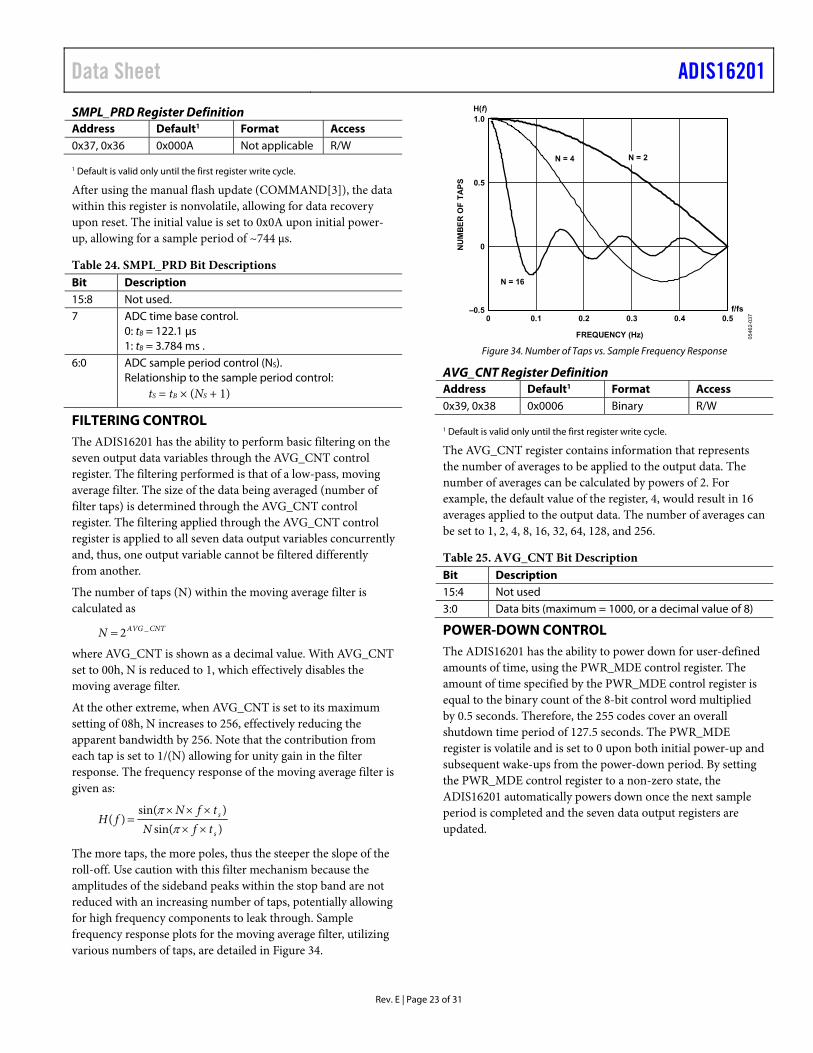
FILTERING CONTROL The ADIS16201 has the ability to perform basic filtering on the seven output data variables through the AVG_CNT control register. The filtering performed is that of a low-pass, moving average filter. The size of the data being averaged (number of filter taps) is determined through the AVG_CNT control register. The filtering applied through the AVG_CNT control register is applied to all seven data output variables concurrently and, thus, one output variable cannot be filtered differently from another.
The number of taps (N) within the moving average filter is calculated as
CNTAVGN _2
where AVG_CNT is shown as a decimal value. With AVG_CNT set to 00h, N is reduced to 1, which effectively disables the moving average filter.
At the other extreme, when AVG_CNT is set to its maximum setting of 08h, N increases to 256, effectively reducing the apparent bandwidth by 256. Note that the contribution from each tap is set to 1/(N) allowing for unity gain in the filter response. The frequency response of the moving average filter is given as:
)sin()sin(
)(s
s
tfNtfN
fH
The more taps, the more poles, thus the steeper the slope of the roll-off. Use caution with this filter mechanism because the amplitudes of the sideband peaks within the stop band are not reduced with an increasing number of taps, potentially allowing for high frequency components to leak through. Sample frequency response plots for the moving average filter, utilizing various numbers of taps, are detailed in Figure 34.
1.0H(f)
–0.50 0.5
f/fs
FREQUENCY (Hz)
NU
MB
ER
OF
TA
PS 0.5
0
0.1 0.2 0.3 0.4
N = 2N = 4
N = 16
05462-037
Figure 34. Number of Taps vs. Sample Frequency Response
AVG_CNT Register Definition Address Default1 Format Access 0x39, 0x38 0x0006 Binary R/W
1 Default is valid only until the first register write cycle.
The AVG_CNT register contains information that represents the number of averages to be applied to the output data. The number of averages can be calculated by powers of 2. For example, the default value of the register, 4, would result in 16 averages applied to the output data. The number of averages can be set to 1, 2, 4, 8, 16, 32, 64, 128, and 256.
Table 25. AVG_CNT Bit Description Bit Description 15:4 Not used 3:0 Data bits (maximum = 1000, or a decimal value of 8)
POWER-DOWN CONTROL The ADIS16201 has the ability to power down for user-defined amounts of time, using the PWR_MDE control register. The amount of time specified by the PWR_MDE control register is equal to the binary count of the 8-bit control word multiplied by 0.5 seconds. Therefore, the 255 codes cover an overall shutdown time period of 127.5 seconds. The PWR_MDE register is volatile and is set to 0 upon both initial power-up and subsequent wake-ups from the power-down period. By setting the PWR_MDE control register to a non-zero state, the ADIS16201 automatically powers down once the next sample period is completed and the seven data output registers are updated.
ADIS16201 Data Sheet
Rev. E | Page 24 of 31
Once the ADIS16201 is placed into the power-down mode, it can only return to normal operation by timing out, a reset command (using the RST hardware control line), or by cycling the power applied to the part. Once awake, the seven data output registers can be scanned to determine what the state of the output registers were prior to powering down. Once the data is recovered, the device can be powered down again by writing a non-zero value to the PWR_MDE control register and starting the process over.
Once the power-down time is complete, the recovery time for the ADIS16201 is approximately 2 ms. This recovery time is implemented within the device to allow for recovery of the ADC prior to performing the next data conversion. Note that the ND data bit within the seven data output control registers is cleared when the ADIS16201 is powered down. Likewise, the new data hardware I/O line is placed into an inactive state prior to being powered down. The DAC is placed into a power-down mode as well, which results in the DAC output dropping to 0 V during the power-down period. All control register settings are retained while powered down with the exception of the PWR_MDE control register, which is reset to 0 prior to power-down.
PWR_MDE Register Definition Address Default1 Format Access 0x3B, 0x3A 0x0000 Binary R/W 1 Default is valid only until the first register write cycle.
The power-down period is determined by multiplying the binary value represented by the data bits times the constant 0.5 seconds. This results in a variable power-down period of 0.5 seconds to 127.5 seconds with 0.5 seconds resolution in the setting. A setting of 0 disables the power-down mode, whereas any non-zero entry places the device in the power-down mode at the next update of the data output registers. The power-down register is volatile and is set to all 0s upon initial power-up and recovery from the power-down mode.
Table 26. PWR_MDE Bit Descriptions Bit Description 15:8 Not used 7:0 Data bits
STATUS FEEDBACK The status control register within the ADIS16201 is utilized in determining the present state of the device. The ability to monitor the device becomes necessary when and if the ADIS16201 has registered an alarm or error condition as indicated by the “alarm enable” (14) within the seven output data registers. The 16-bit status register is broken into two bytes. The three lower bits of the lower data byte are used to indicate which error condition exists, while the two lower bits of the upper data byte are utilized in indicating which alarm condition exists.
STATUS Register Definition Address Default1 Format Access 0x3D, 0x3C 0x0000 Not applicable Read only
1 Default is valid only until the first register write cycle.
The STATUS control register contains the alarm/error flags that indicate abnormal operating conditions. See Table 27 for each status bit definition. All flags are cleared upon the reading of the status register. The flags are set on a continuing basis as long as the error or alarm conditions persist.
Table 27. STATUS Bit Descriptions Bit Description 15:10 Not used. 9 Alarm 2 status.
1: Active 0: Normal mode
8 Alarm 1 status. 1: Active 0: Normal mode
7:4 Not used. 3 SPI communications failure.
1: Error condition 0: Normal mode
2 Control register update failed. 1: Error condition 0: Normal mode
1 Power supply above 3.625 V. 1: Error condition 0: Normal mode
0 Power supply below 2.975 V. 1: Error condition 0: Normal mode
COMMAND CONTROL The COMMAND control register is utilized in sending global commands to the ADIS16201 device. There are four separate commands that act as global commands in the controlling of the ADIS16201 operation. Any one of the four commands can be implemented by writing 1 to its corresponding bit location. The command control register has write-only capability and is volatile. Table 28 describes each of these global commands.
COMMAND Register Definition Address Default1 Format Access 0x3F, 0x3E 0x0000 Not applicable Write only 1 Default is valid only until the first register write cycle.
Data Sheet ADIS16201
Rev. E | Page 25 of 31
Table 28. COMMAND Bit Descriptions Bit Description 15:8 Not used. 7 Software Reset Command. Allows for resetting of the
device via the SPI.
6:4 Not used. 3 Manual Flash Update Command. This command is
utilized in updating all of the nonvolatile registers to flash. Once the command is initiated, the supply voltage, VDD, must remain within specified limits for 50 ms to assure proper update of the nonvolatile registers to flash.
2 Auxiliary DAC Latch Command. This command acts to latch the AUX_DAC control register data into the auxiliary DAC upon receipt of the command. This allows for sequential loading of the upper and lower AUX_DAC data bytes via the SPI without having the auxiliary DAC transition into unwanted, intermediate states based upon the individual AUX_DAC data bytes. Once the two bytes of AUX_DAC are loaded, the DAC latch command is initiated to move the data into the auxiliary DAC itself.
1 Factory Reset Command. Allows the user to reset all four system level offset registers and all four system level scale registers to the nominal settings (000h and 800h, respectively) upon receipt of command. Data within the moving average filters will likewise be reset. As the manual flash command identified below, this command stores all of the nonvolatile registers to flash. Once the command is initiated, the supply voltage, VDD, must remain within specified limits for 50 ms to assure proper update of the nonvolatile registers to flash.
0 Null Command. Loads the X/Y inclination offset as well as the X/Y acceleration offset registers with values that zero out the inclination and acceleration outputs. Useful as a single command to simultaneously zero both inclination and acceleration outputs. As the manual flash command identified below, this command stores all of the nonvolatile registers to flash. Once the command is initiated, the supply voltage, VDD, must remain within specified limits for 50 ms to assure proper update of the nonvolatile registers to flash.
MISCELLANEOUS CONTROL REGISTER The MSC_CTRL control register within the ADIS16201 provides control of two miscellaneous functions: the data-ready hardware I/O function and the self-test function. The bits to control these two functions are shown in Table 29.
The operation of the data-ready hardware I/O function is very similar to the alarm hardware I/O function (controlled through the ALM_CTRL control register). In this case, the MSC_CNTRL register can be used in setting up one of the two GPIO pins to serve as the hardware output pin that indicates when the sampling, conversion, and processing of the seven data output variables has been completed. This register provides the ability to enable the data-ready hardware function and establish its polarity.
The data-ready hardware I/O pin is reset automatically to an inactive state part way through the next conversion cycle, resulting in a pulse train with a duty cycle varying from ~15% to 35%, depending upon the sample period setting. Upon completion of the next sample/conversion/processing cycle, the data ready hardware I/O line is reasserted.
The MSC_CTRL, ALM_CTRL, and GPIO_CTRL control registers can influence the same GPIO pins. A priority level has been established to avoid conflicting assignments of the two GPIO pins. This priority level is defined as MSC_CTRL and has precedence over ALM_CTRL, which has precedence over GPIO_CTRL.
The self-test enable bit allows the user to place the ADIS16201 into a diagnostics mode for purposes of verifying the operation of the base sensor. When this bit is set high, an electrostatic force is generated internally to the sensor. The resulting movement within the sensor allows the end user to test if the accelerometer is functional. Typical change in the output is 328 mg (corresponding to 708 LSB). Once the self-test enable bit is returned to a low state, normal operation is resumed.
MSC_CTRL Register Definition Address Default1 Format Access 0x35, 0x34 0x0000 Not applicable R/W 1 Default is valid only until the first register write cycle.
The 16-bit miscellaneous control register is used in the controlling of the self-test and data-ready hardware functions. This includes turning on and off the self-test function, as well as enabling and configuring the data-ready function. For the data-ready function, the written values are nonvolatile, allowing for data recovery upon reset. The self-test data is volatile and is set to 0s upon reset. This register has read/write capability.
Table 29. MSC_CTRL Bit Descriptions Bit Description 15:9 Not used. 8 Self-test enable.
1: ST enabled 0: ST disabled
7:3 Not used. 2 Data-ready enable.
1: DR enabled 0: DR disabled
1 Data-ready polarity. 1: Active high 0: Active low
0 Data-ready line select. 1: DIO1 0: DIO0
ADIS16201 Data Sheet
Rev. E | Page 26 of 31
PERIPHERALS AUXILIARY ADC FUNCTION The auxiliary ADC function integrates a standard 12-bit ADC into the ADIS16201 to digitize other system-level analog signals. The output of the ADC can be monitored through the AUX_ADC control register, as defined in Table 6 and Table 7. The ADC consists of a 12-bit successive approximation converter. The output data is presented in straight binary format, with the full-scale range extending from 0 V to VREF. A high precision, low drift, factory-calibrated 2.5 V reference is also provided.
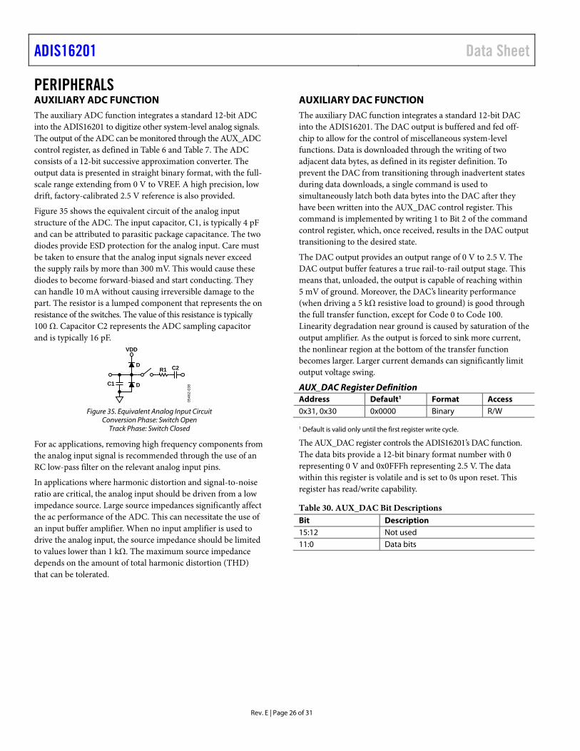
Figure 35 shows the equivalent circuit of the analog input structure of the ADC. The input capacitor, C1, is typically 4 pF and can be attributed to parasitic package capacitance. The two diodes provide ESD protection for the analog input. Care must be taken to ensure that the analog input signals never exceed the supply rails by more than 300 mV. This would cause these diodes to become forward-biased and start conducting. They can handle 10 mA without causing irreversible damage to the part. The resistor is a lumped component that represents the on resistance of the switches. The value of this resistance is typically 100 Ω. Capacitor C2 represents the ADC sampling capacitor and is typically 16 pF.
C2
C1
R1
VDD
D
D
0546
2-03
8
Figure 35. Equivalent Analog Input Circuit
Conversion Phase: Switch Open Track Phase: Switch Closed
For ac applications, removing high frequency components from the analog input signal is recommended through the use of an RC low-pass filter on the relevant analog input pins.
In applications where harmonic distortion and signal-to-noise ratio are critical, the analog input should be driven from a low impedance source. Large source impedances significantly affect the ac performance of the ADC. This can necessitate the use of an input buffer amplifier. When no input amplifier is used to drive the analog input, the source impedance should be limited to values lower than 1 kΩ. The maximum source impedance depends on the amount of total harmonic distortion (THD) that can be tolerated.
AUXILIARY DAC FUNCTION The auxiliary DAC function integrates a standard 12-bit DAC into the ADIS16201. The DAC output is buffered and fed off-chip to allow for the control of miscellaneous system-level functions. Data is downloaded through the writing of two adjacent data bytes, as defined in its register definition. To prevent the DAC from transitioning through inadvertent states during data downloads, a single command is used to simultaneously latch both data bytes into the DAC after they have been written into the AUX_DAC control register. This command is implemented by writing 1 to Bit 2 of the command control register, which, once received, results in the DAC output transitioning to the desired state.
The DAC output provides an output range of 0 V to 2.5 V. The DAC output buffer features a true rail-to-rail output stage. This means that, unloaded, the output is capable of reaching within 5 mV of ground. Moreover, the DAC’s linearity performance (when driving a 5 kΩ resistive load to ground) is good through the full transfer function, except for Code 0 to Code 100. Linearity degradation near ground is caused by saturation of the output amplifier. As the output is forced to sink more current, the nonlinear region at the bottom of the transfer function becomes larger. Larger current demands can significantly limit output voltage swing.
AUX_DAC Register Definition Address Default1 Format Access 0x31, 0x30 0x0000 Binary R/W 1 Default is valid only until the first register write cycle.
The AUX_DAC register controls the ADIS16201’s DAC function. The data bits provide a 12-bit binary format number with 0 representing 0 V and 0x0FFFh representing 2.5 V. The data within this register is volatile and is set to 0s upon reset. This register has read/write capability.
Table 30. AUX_DAC Bit Descriptions Bit Description 15:12 Not used 11:0 Data bits
Data Sheet ADIS16201
Rev. E | Page 27 of 31
GENERAL PURPOSE I/O CONTROL As previously noted, the ADIS16201 provides two general-purpose, bidirectional I/O pins (GPIOs) that are available to the user for control of auxiliary circuits within the target application. All I/O pins are 5 V tolerant, meaning that the GPIOs support an input voltage of 5 V. All GPIO pins have an internal pull-up resistor of approximately 100 kΩ, and their drive capability is 1.6 mA. The direction, as well as the logic level, can be controlled for these GPIO pins through the GPIO_CTRL control register, as defined in Table 31.
These same GPIO pins are also controllable through the ALM_CTRL and MSC_CTRL control registers. The priority for these three control registers in controlling the two GPIO pins is MSC_CTRL has precedence over ALM_CTRL, which has precedence over GPIO_CTRL.
GPIO_CTRL Register Definition Address Default1 Format Access 0x33, 0x32 0x0000 Not applicable R/W 1 Default is valid only until the first register write cycle.
Auxiliary Digital I/O Control Register. The data within this register is volatile and is set to 0s upon reset.
Table 31. GPIO_CTRL Bit Descriptions Bit Description 15:10 Not used. 9 General-Purpose I/O Line 1 polarity.
0: Low 1: High
8 General-Purpose I/O Line 0 polarity. 0: Low 1: High
7:2 Not used. 1 General-Purpose I/O Line 1, data direction control.
0: Input 1: Output
0 General-Purpose I/O Line 0, data direction control. 0: Input 1: Output
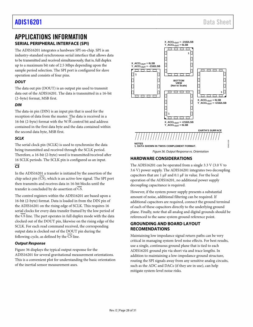
ADIS16201 Data Sheet
Rev. E | Page 28 of 31
APPLICATIONS INFORMATION SERIAL PERIPHERAL INTERFACE (SPI) The ADIS16201 integrates a hardware SPI on-chip. SPI is an industry-standard synchronous serial interface that allows data to be transmitted and received simultaneously, that is, full duplex up to a maximum bit rate of 2.5 Mbps depending upon the sample period selection. The SPI port is configured for slave operation and consists of four pins.
DOUT
The data out pin (DOUT) is an output pin used to transmit data out of the ADIS16201. The data is transmitted in a 16-bit (2–byte) format, MSB first.
DIN
The data-in pin (DIN) is an input pin that is used for the reception of data from the master. The data is received in a 16-bit (2-byte) format with the W/R control bit and address contained in the first data byte and the data contained within the second data byte, MSB first.
SCLK
The serial clock pin (SCLK) is used to synchronize the data being transmitted and received through the SCLK period. Therefore, a 16-bit (2-byte) word is transmitted/received after 16 SCLK periods. The SCLK pin is configured as an input.
CS
In the ADIS16201 a transfer is initiated by the assertion of the chip select pin (CS), which is an active-low signal. The SPI port then transmits and receives data in 16-bit blocks until the transfer is concluded by de-assertion of CS.
The control registers within the ADIS16201 are based upon a 16-bit (2-byte) format. Data is loaded in from the DIN pin of the ADIS16201 on the rising edge of SCLK. This requires 16 serial clocks for every data transfer framed by the low period of the CS line. The part operates in full duplex mode with the data clocked out of the DOUT pin, likewise on the rising edge of the SCLK. For each read command received, the corresponding output data is clocked out of the DOUT pin during the following cycle, as defined by the CS line.
Output Response
Figure 36 displays the typical output response for the ADIS16201 for several gravitational measurement orientations. This is a convenient plot for understanding the basic orientation of the inertial sensor measurement axes.
BOTTOMVIEW
(Not to Scale)
1
1
1
1
X_ACCLOUT = 0LSBY_ACCLOUT = –2162LSB
NOTES1. DATA SHOWN IN TWOS COMPLEMENT FORMAT.
X_ACCLOUT = 0LSBY_ACCLOUT = +2162LSB
X_ACCLOUT = –2162LSBY_ACCLOUT = 0LSB
X_ACCLOUT = +2162LSBY_ACCLOUT = 0LSB
EARTH’S SURFACE
0546
2-03
9
Figure 36. Output Response vs. Orientation
HARDWARE CONSIDERATIONS The ADIS16201 can be operated from a single 3.3 V (3.0 V to 3.6 V) power supply. The ADIS16201 integrates two decoupling capacitors that are 1 μF and 0.1 μF in value. For the local operation of the ADIS16201, no additional power supply decoupling capacitance is required.
However, if the system power supply presents a substantial amount of noise, additional filtering can be required. If additional capacitors are required, connect the ground terminal of each of these capacitors directly to the underlying ground plane. Finally, note that all analog and digital grounds should be referenced to the same system ground reference point.
GROUNDING AND BOARD LAYOUT RECOMENDATIONS Maintaining low impedance signal return paths can be very critical in managing system-level noise effects. For best results, use a single, continuous ground plane that is tied to each ADIS16201 ground pin via short via and trace lengths. In addition to maintaining a low-impedance ground structure, routing the SPI signals away from any sensitive analog circuits, such as the ADC and DACs (if they are in use), can help mitigate system-level noise risks.
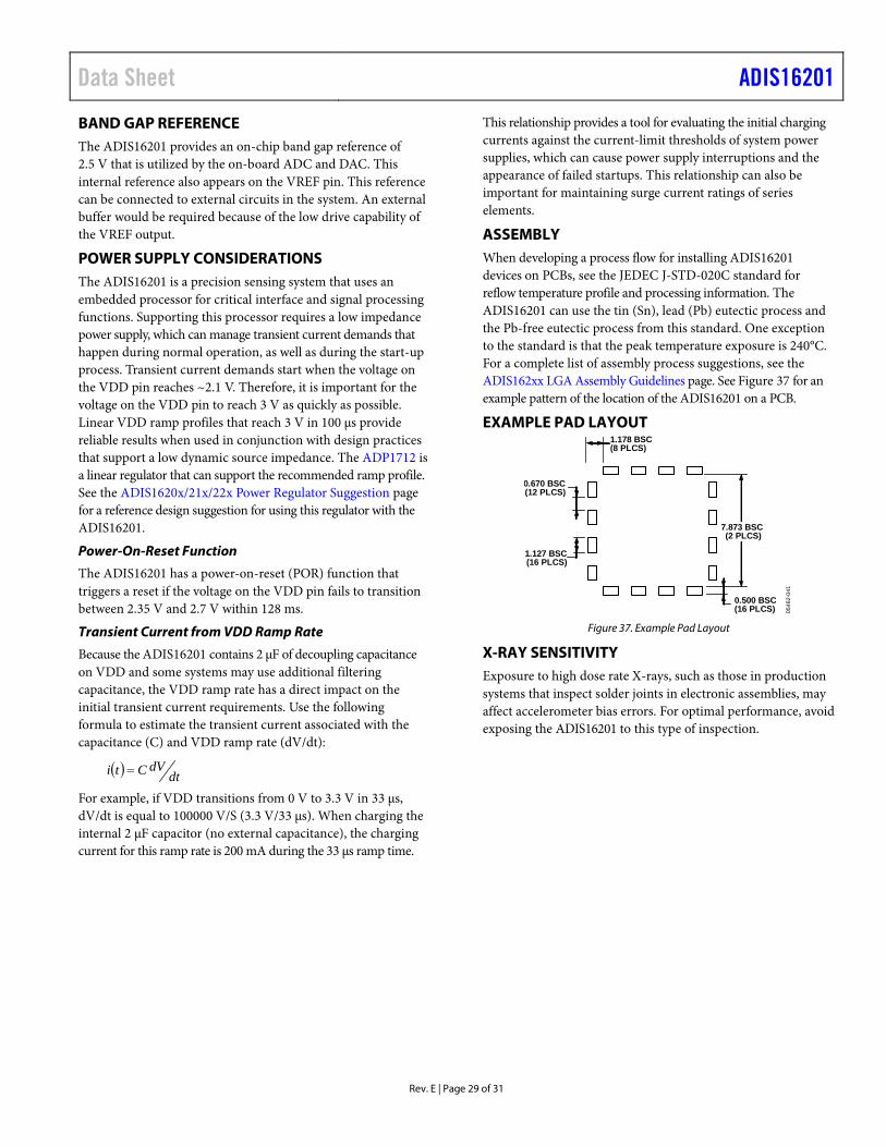
Data Sheet ADIS16201
Rev. E | Page 29 of 31
BAND GAP REFERENCE The ADIS16201 provides an on-chip band gap reference of 2.5 V that is utilized by the on-board ADC and DAC. This internal reference also appears on the VREF pin. This reference can be connected to external circuits in the system. An external buffer would be required because of the low drive capability of the VREF output.
POWER SUPPLY CONSIDERATIONS The ADIS16201 is a precision sensing system that uses an embedded processor for critical interface and signal processing functions. Supporting this processor requires a low impedance power supply, which can manage transient current demands that happen during normal operation, as well as during the start-up process. Transient current demands start when the voltage on the VDD pin reaches ~2.1 V. Therefore, it is important for the voltage on the VDD pin to reach 3 V as quickly as possible. Linear VDD ramp profiles that reach 3 V in 100 µs provide reliable results when used in conjunction with design practices that support a low dynamic source impedance. The ADP1712 is a linear regulator that can support the recommended ramp profile. See the ADIS1620x/21x/22x Power Regulator Suggestion page for a reference design suggestion for using this regulator with the ADIS16201.
Power-On-Reset Function
The ADIS16201 has a power-on-reset (POR) function that triggers a reset if the voltage on the VDD pin fails to transition between 2.35 V and 2.7 V within 128 ms.
Transient Current from VDD Ramp Rate
Because the ADIS16201 contains 2 μF of decoupling capacitance on VDD and some systems may use additional filtering capacitance, the VDD ramp rate has a direct impact on the initial transient current requirements. Use the following formula to estimate the transient current associated with the capacitance (C) and VDD ramp rate (dV/dt):
( ) dtdVCti =
For example, if VDD transitions from 0 V to 3.3 V in 33 µs, dV/dt is equal to 100000 V/S (3.3 V/33 µs). When charging the internal 2 µF capacitor (no external capacitance), the charging current for this ramp rate is 200 mA during the 33 µs ramp time.
This relationship provides a tool for evaluating the initial charging currents against the current-limit thresholds of system power supplies, which can cause power supply interruptions and the appearance of failed startups. This relationship can also be important for maintaining surge current ratings of series elements.
ASSEMBLY When developing a process flow for installing ADIS16201 devices on PCBs, see the JEDEC J-STD-020C standard for reflow temperature profile and processing information. The ADIS16201 can use the tin (Sn), lead (Pb) eutectic process and the Pb-free eutectic process from this standard. One exception to the standard is that the peak temperature exposure is 240°C. For a complete list of assembly process suggestions, see the ADIS162xx LGA Assembly Guidelines page. See Figure 37 for an example pattern of the location of the ADIS16201 on a PCB.
EXAMPLE PAD LAYOUT 1.178 BSC(8 PLCS)
0.500 BSC(16 PLCS)
1.127 BSC(16 PLCS)
0.670 BSC(12 PLCS)
7.873 BSC(2 PLCS)
0546
2-04
1
Figure 37. Example Pad Layout
X-RAY SENSITIVITY Exposure to high dose rate X-rays, such as those in production systems that inspect solder joints in electronic assemblies, may affect accelerometer bias errors. For optimal performance, avoid exposing the ADIS16201 to this type of inspection.
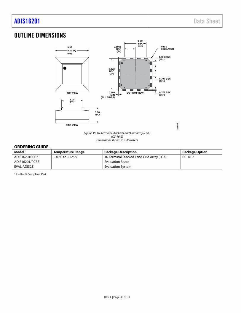
ADIS16201 Data Sheet
Rev. E | Page 30 of 31
OUTLINE DIMENSIONS
1 214
0 9-CSIDE VIEW
TOP VIEW BOTTOM VIEW
PIN 1INDICATOR
1.000 BSC(16×)
3.90MAX
1
458
9
1213 16
5.391BSC(4×)2.6955
BSC(8×)
5.00TYP
8.373BSC(2×)
0.200MIN
(ALL SIDES)
0.797 BSC(12×)
0.373 BSC(16×)
9.359.20 SQ9.05
Figure 38. 16-Terminal Stacked Land Grid Array [LGA]
(CC-16-2) Dimensions shown in millimeters
ORDERING GUIDE Model1 Temperature Range Package Description Package Option ADIS16201CCCZ −40°C to +125°C 16-Terminal Stacked Land Grid Array [LGA] CC-16-2 ADIS16201/PCBZ Evaluation Board EVAL-ADIS2Z Evaluation System 1 Z = RoHS Compliant Part.

Data Sheet ADIS16201
Rev. E | Page 31 of 31
NOTES
©2006–2019 Analog Devices, Inc. All rights reserved. Trademarks and registered trademarks are the property of their respective owners. D05462-0-3/19(E)