radio frequency integrated circuits - 博九娱乐网络娱...
TRANSCRIPT

1Shuenn-Yuh Lee EE/CCU Chapter 1Communication and Biologic IC Lab.
Radio Frequency Integrated Circuits
Instructor : Shuenn-Yuh Lee
National Chung Cheng UniversityDepartment of Electrical Engineering
Office : 431 TEL : (05)2720411-33223, BP : 0921565137E-mail : [email protected]
Table of Content : 1. Basic Concepts in RF Design2. Modulation and Detection3. Multiple Access Techniques and Wireless Standards4. Transceiver Architectures5. Transmission line and match networks6. LNA and Mixer7. Oscillators8. Phase-Locked Loops9. Frequency Synthesizer10. Power Amplifier

2Shuenn-Yuh Lee EE/CCU Chapter 1Communication and Biologic IC Lab.
數位邏輯設計與實習
數位系統設計與實習 電子學
VLSI設計導論與實習
混合訊號佈局設計 類比積體電路
數位系統快速雛型設計 混合訊號積體電路
VLSI測試理論
VLSI設計流程整合實務
MOS元件分析與模擬
SOC導論
訊號處理架構設計VLSI系統設計與高階合成
類比與混合積體電路測試通訊積體電路設計
射頻積體電路設計
射頻通訊概論
課程規劃流程

3Shuenn-Yuh Lee EE/CCU Chapter 1Communication and Biologic IC Lab.
Reference Books• Texbook : RF Microelectronics, Behzad Razavi, 1998
• Design of Analog CMOS Integrated Circuits, Behzad Razavi, 2001
• The Design of CMOS Radio-Frequency Integrated Circuits, 1998
• Analog Integrated Circuit Design, David A. Johns, and Ken Martin, 1997
• CMOS Analog Circuit Design, Second Edition, Phillip E. Allen ,and Douglas R.
Holberg, 2002
• Circuit Design for RF Transceivers, Domine Leenaerts, Hohan van der Tang, and
Cicero Vaucher, 2001
• Architectures for RF Frequency Synthesizers, Cicero S. Vaucher, 2002
• Phase-Locked Loops for Wireless Communications : Digital, Analog and Optical
Implementations, Second Edition, 2002
Grade Factors1. Homework 30%, Project 70%

4Shuenn-Yuh Lee EE/CCU Chapter 1Communication and Biologic IC Lab.
Introduction to Wireless Systems
• Complexity Comparison
• Design Bottleneck
• Applications
• Analog and Digital Systems
• Choice of Technology
• Effect of Nonlinearity

5Shuenn-Yuh Lee EE/CCU Chapter 1Communication and Biologic IC Lab.
Complexity Comparison• A simple FM transceiver
– FM transmitter
Q1operates as both oscillator and a
frequency modulator
– FM receiver
Q1operates as both oscillator and a
frequency demodulator

6Shuenn-Yuh Lee EE/CCU Chapter 1Communication and Biologic IC Lab.
• RF section of a cellphone– This circuit is orders of magnitude more complex than analog FM circuit
Complexity Comparison (Cont.)

7Shuenn-Yuh Lee EE/CCU Chapter 1Communication and Biologic IC Lab.
Design Bottleneck• RF and baseband processing in a transceiver
– The baseband section is more complex – The RF section is still the design bottleneck of
the entire system
• Three reasons– Disciplines required in RF design– RF design Hexagon
– Design toolsComputer-aided analysis and synthesis tools for RF ICs are still in theirinfancy

8Shuenn-Yuh Lee EE/CCU Chapter 1Communication and Biologic IC Lab.
• PCS (person communication system)
– Pagers and Cellular phones
• WLANs (wireless local area network)
• GPS (global positioning system)
• RF IDs (RF identification systems)
• Home Satellite Network
Applications

9Shuenn-Yuh Lee EE/CCU Chapter 1Communication and Biologic IC Lab.
Analog and Digital Systems• Block diagram of a generic analog RF system
– (a) transmitter (b) receiver

10Shuenn-Yuh Lee EE/CCU Chapter 1Communication and Biologic IC Lab.
• Block diagram of a generic digital RF system– (a) transmitter, (b) receiver– voice compression : reduce bit rate and required bandwidth– coding and interleaving : reduce the bit error rate
– pulse shaping : shape the rectangular pulse
Analog and Digital Systems (Cont.)

11Shuenn-Yuh Lee EE/CCU Chapter 1Communication and Biologic IC Lab.
Choice of Technology• Performance,cost,and time to market are three critical
factors influencing the choice of technologies in the
competitive RF industry
• Level of integration,form factor, and prior(successful)
experience play an important role in the decisions made by
the designers
• Must resolve a number of practical issues
– Substrate coupling of signals that differ in amplitude by 100 dB
– Parameter variation with temperature and process.
– Device modeling for RF operation (been resolved)

12Shuenn-Yuh Lee EE/CCU Chapter 1Communication and Biologic IC Lab.
Choice of Technology (Cont.)• GaAs
– High frequency, high power, and high cost
– Widely used in power amplifier and front-end switched
• Silicon Bipolar
– Higher integration, high power, and lower cost
– Widely used in transceiver
• CMOS
– Highest integration, lowest cost, and low power
– Low operation frequency

13Shuenn-Yuh Lee EE/CCU Chapter 1Communication and Biologic IC Lab.
Basic Concepts in RF Design
Outline• Nonlinearity and Time Variance
– Effects of Nonlinearity
– Cascaded Nonlinear Stages
• Intersymbol Interference
• Random Processes and Noise
– Random Processes
– Noise
• Sensitivity and Dynamic Range
• Passive Impedance Transformation

14Shuenn-Yuh Lee EE/CCU Chapter 1Communication and Biologic IC Lab.
Nonlinearity and Time Variance• Linear system
for all values of the constants a and b
• Nonlinear system– Not satisfy above condition– With nonzero initial conditions or
finite “offsets”
• Time invariant
),()()()()()(,)()(
2121
2211
tbytaytbxtaxtytxtytx
+→+→→
)()(,)()( ττ −→−→ tytxtytxwe assume the switch is on if vin1>0 and off otherwise.
tAtvtAtv
in
in
222
111
cos)(cos)(
ωω
==
•Simple switching circuit •Nonlinear time-variant system
The path of interest is from vin1 to vout. The system is nonlinear because the control is only sensitive to the polarity of vin1, and time variant because vout also depends on vin2

15Shuenn-Yuh Lee EE/CCU Chapter 1Communication and Biologic IC Lab.
( )
( )
−=
−∗=
∑
∑∞+
−∞=
+∞
−∞=
12
12
2/sin
2/sin)()(
Tnfv
nn
Tnf
nnfvfv
inn
ninout
ππ
δππ
Nonlinearity and Time Variance (Cont.)• Linear time-variant system
– The path of interest is from vin2 to vout, then the system is linear but time variant
– Vout can also be considered as the product of vin2 and a square wave toggling between 0 and 1

16Shuenn-Yuh Lee EE/CCU Chapter 1Communication and Biologic IC Lab.
Memoryless• Its output does not depend on the past value of its input
• For a memoryless linear system
• For a memoryless nonlinear system
)()( txty α=
L++++= )()()()( 33
2210 txtxtxty αααα
Equivalent
RtsVvItvT
inSout ⋅
= )(exp)( 1

17Shuenn-Yuh Lee EE/CCU Chapter 1Communication and Biologic IC Lab.
Odd symmetry and dynamic• Odd symmetry (called differential or balanced)
– For x(t)→-x(t) :– Example : bipolar differential pair
• Dynamic : if its output depends on the past values of its input(s) or output(s)– Linear time-invariant, dynamic system
– Linear time-variant, dynamic system
h(t) denotes the impulse response
L+−+−= )()()()( 33
2210 txtxtxty αααα
)(*)()( txthty =
)(*),()( txthty τ=
T
inEEout V
vRIv2
tanh=
( )( )
TinTin
TinTin
TinTin
TinTin
TinTin
TinTin
VVVV
VVVV
EE
VVVV
VVVV
EEccout
VVEE
cVVC
VVEE
cVVC
eeeeRI
eeeeRIVVV
eRIV
eIi
eRIV
eIi
2/2/
2/2/
//
//
21
/2/2
/1/1
1111
11
11
−
−
−
−
−−
+−
=
++−−+
=−=
+≈⇒
+=
+≈⇒
+=
α
α

18Shuenn-Yuh Lee EE/CCU Chapter 1Communication and Biologic IC Lab.
Effects of Nonlinearity• For memoryless, time-variant, nonlinear system
)()()()( 33
221 txtxtxty ααα ++≈
• Effects of nonlinearity
– Harmonics
– Gain compression
– Desensitization and blocking
– Cross modulation
– Intermodulation

19Shuenn-Yuh Lee EE/CCU Chapter 1Communication and Biologic IC Lab.
Harmonics• If x(t)=Acosωt, and )()()()( 3
32
21 txtxtxty ααα ++≈
• Two observations– Odd symmetry : Even-order harmonics result from αj with enen j are
vanish– The amplitude of the n th harmonic consists of a term proportional to An
Harmonics
tAtAtAAA
tAtAtAty
ωαωαωααα
ωαωαωα
3cos4
2cos2
cos4
32
coscoscos)(3
32
23
31
22
333
2221
++
++=
++=

20Shuenn-Yuh Lee EE/CCU Chapter 1Communication and Biologic IC Lab.
• For small-signal gain of a circuit , harmonics are negligible– For example, α1A is much greater than all the other factors that contain
A, then the small-signal gain is equal to α1
– For bipolar differential pair
• In most circuit of interest, the output is a “compressive”or ”saturating” function of the input – Gain = α1+3α3A2/4, where α3 < 0, and A ↑ ⇒ gain ↓
• 1-dB compression point
RgVRI
vv
mT
EE
in
out ===21α
Gain Compression
3
11
12
131
145.0
1log2043log20log20
αα
ααα
=
−=+=
−
−
dB
dBin
out
Athen
dBAAA

21Shuenn-Yuh Lee EE/CCU Chapter 1Communication and Biologic IC Lab.
Desensitization and Blocking• Desensitization
– A weak,desired signal along with a strong interferer.
– Since a large signal tends to reduce the ”average” gain of the circuit,the weak signal may experience a vanishingly small gain. Called ”desensitization”
• Blocking:– Gain= (α1+3α3A2
2/2) , A2 ↑ ⇒ gain ↓ ⇒ gain = 0 ⇒called “blocked”
– In RF design,the term”blocking signal” usually refers to interferers that desensitize a circuit even if the gain does not fall to zero
– Many RF receivers must be able to withstand blocking signals 60 to 70 dB greater than the wanted signal
L
L
+
+=
+
++=
<<+=
tAA
tAAAAty
AAfortAtAtx
112231
12213
31311
21
2211
cos23
cos23
43)(
coscos)(
ωαα
ωααα
ωω

22Shuenn-Yuh Lee EE/CCU Chapter 1Communication and Biologic IC Lab.
Cross Modulation
• A weak signal and a strong interferer pass through a
nonlinear system
– For example : If the amplitude of the interferer is modulated by a
sinusoid A2(1+mcosωmt)cos ω2t
( )
L+
++++=
++=
tAtmtmmAty
ttmAtAtx
mm
m
11
222231
2211
coscos22cos22
123)(
coscos1cos)(
ωωωαα
ωωω
– Desired signal at the output contains amplitude modulation at ωm and 2 ωm
– Cross modulation arises in amplifiers that must simultaneously process many independent signal channels

23Shuenn-Yuh Lee EE/CCU Chapter 1Communication and Biologic IC Lab.
• Harmonics distortion in a low-pass filter : fall out of the passband
Intermodulation (IM)
• Intermodulation distortion (two tone test)
– When two signals with different frequencies are applied to a
nonlinear system,the output in general exhibits some
components that are not harmonics of the input frequencies
– This phenomenon arises from “mixing”(multiplication) of the
two signals

24Shuenn-Yuh Lee EE/CCU Chapter 1Communication and Biologic IC Lab.
Third-order IM product• Assume x(t)=A1cosω1t+ A2cosω2t, thus
• Intermodulation product
• Fundamental components
( ) ( )
( ) ( )
( ) ( )tAAtAA
tAAtAA
tAAtAA
121
223
121
223
12
212
213
212
213
21
212122121221
2cos4
32cos4
3:2
2cos4
32cos4
3:2
coscos:
ωωαωωαωω
ωωαωωαωω
ωωαωωαωωω
−++±=
−++±=
−++±=
tAAAA
tAAAA
22
12332321
12213
3131121
cos23
43
cos23
43:,
ωααα
ωαααωωω
+++
++=
322113
22211222111 )coscos()coscos()coscos()( tAtAtAtAtAtAty ωωαωωαωωα +++++=

25Shuenn-Yuh Lee EE/CCU Chapter 1Communication and Biologic IC Lab.
Third-order IM product effect• Intermodulation in a nonlinear system
– Assume A1=A2=A
• Corruption of a signal due to Intermodulation– For example : if α1A=1Vpp, and 3 α3A2/4=10mVpp
⇒ the IM components are at -40dBc
26Shuenn-Yuh Lee EE/CCU Chapter 1Communication and Biologic IC Lab.
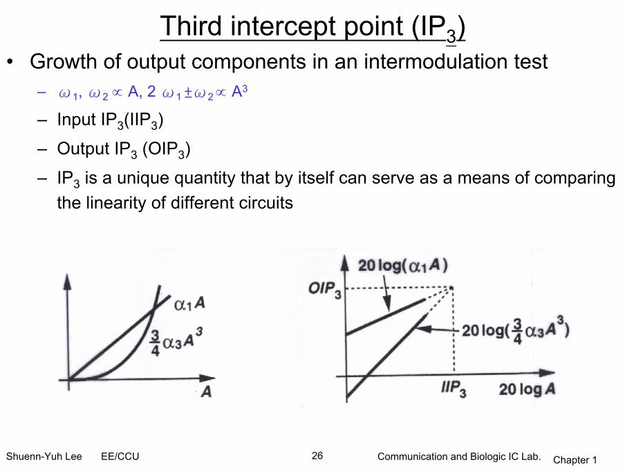
Third intercept point (IP3)• Growth of output components in an intermodulation test
– ω1, ω2 ∝ A, 2 ω1 ±ω2 ∝ A3
– Input IP3(IIP3)
– Output IP3 (OIP3)
– IP3 is a unique quantity that by itself can serve as a means of comparing the linearity of different circuits

27Shuenn-Yuh Lee EE/CCU Chapter 1Communication and Biologic IC Lab.
IP3 calculation• Let x(t)=Acosω1t+Acos ω2t
– If α1>>9 α3A2/4 – Input IP3=AIP3 and output IP3=α1AIP3
( ) ( ) L+−+−+
++
+=
tAtA
tAAtAAty
123
3213
3
22
3112
31
2cos432cos
43
cos49cos
49)(
ωωαωωα
ωααωαα
3
13
33331
34
43
αα
αα
=⇒
=
IP
IPIP
A
AA

28Shuenn-Yuh Lee EE/CCU Chapter 1Communication and Biologic IC Lab.
Quick IP3 measurement• Denote : Ain : the input level at each frequency
Aω1, ω2 : the amplitude of the output at ω1, ω2
AIM3 : the amplitude of the IM3 product• Quick method
( ) inIMIP
inIPIM
in
IP
inin
in
IM
AAAA
AAAA
AA
AAA
AA
log20log20log2021log20
log20log20log20log20
134
4/3
32,13
22332,1
2
23
23
13
3
1
3
2,1
+−=⇒
−=−⇒
==≈
ωω
ωω
ωω
αα
αα

29Shuenn-Yuh Lee EE/CCU Chapter 1Communication and Biologic IC Lab.
Example• Asig,in=1µVrms, AIP3=70mVrms (≅-10dBm), Aint,in=1mVrms
– Asig,in : signal amplitude, Aint,in : interferer amplitude
• Relation between A1-dB and AIP3
( )( ) dB
AAA
AA
AA
AA
AAA
AAA
AA
in
IPinsig
outIM
out
in
insig
outIM
outsig
outin
insigoutsig
in
out
insig
outsig
8.139.4101
10701033
236
3int,
23,
,3
int,
int,
,
,3
,
int,int,
,,
int,
int,
,
,
≈=×
××=
⋅==⇒
=⇒≈
−
−−
dBAA
IP
dB 6.9
34
145.0
3
1
3
1
3
1 −≈=−
αα
αα

30Shuenn-Yuh Lee EE/CCU Chapter 1Communication and Biologic IC Lab.
Cascaded nonlinear stage
[ ][ ][ ]
( ) L++++=
+++
+++
++=⇒
++=
++=
)(2)(
)()()(
)()()(
)()()()(
)()()()(
)()()()(
33
312211311
333
2213
233
2212
33
22112
313
212112
33
2211
txtx
txtxtx
txtxtx
txtxtxty
tytytyty
txtxtxty
βαβααβαβα
αααβ
αααβ
αααβ
βββ
ααα
33122113
113 23
4βαβααβα
βα++
=IPA
• Proper choice of the values and signs of the terms in the denominator can yield an high IP3
• As a worst-case estimate, relations among AIP3, AIP3,1 and AIP3,2
– α1↑, the overall IP3 ↓, because with higher gain in the first stage, the second stage sense large input level, thereby producing much greater IM3 products
22,3
21
1
222
1,311
33122113
23 2
312431
IPIPIP AAAα
ββα
βαβαβααβα
++=++
=

31Shuenn-Yuh Lee EE/CCU Chapter 1Communication and Biologic IC Lab.
Intermodulation in cascade of two stage
L+++= 23,3
21
21
22,3
21
21,3
23
11
IPIPIPIP AAAAβαα
• General expression for three or more stages

32Shuenn-Yuh Lee EE/CCU Chapter 1Communication and Biologic IC Lab.
Intersymbol interference• Linear time-invariant systems can also “distort” a signal if they
do not have sufficient bandwidth– Example : low-pass filter
• Intersymbol interference (ISI)– Each bit level is corrupted by decaying tails created by
previous bits– Leads to higher error rate in the detection of random
waveforms– Reduce ISI methods : pulse shaping in the transmitter
equalization in the receiver

33Shuenn-Yuh Lee EE/CCU Chapter 1Communication and Biologic IC Lab.
Pulse shape• It is less susceptible to interference with its shifted replicas
– All other pulse go through zero at the point when the present pulse reaches its peak
– If the bit stream is sampled at t=KTs, no ISI exists
• For a pulse shape, p(t)
• Nyquist’s condition for the spectrum of a pulse shape that gives no ISI– Using a train of impulses to sample this pulse
0001)(≠=
==kifkifkTp s
11
11)(
)()()(
=
−⇒
=
−∗⇒
=−⋅
∑
∑
∑
ss
ss
transformFourier
s
TkfP
T
Tkf
TfP
tkTttp
δ
δδ

34Shuenn-Yuh Lee EE/CCU Chapter 1Communication and Biologic IC Lab.
Raised cosine filter• Pulse shape design problem
– The filter required to produce the rectangular spectrum becomes quite complex in both the transmit and receive paths
– The sinc waveform decays slowly with time, introducing considerable ISI in the presence of timing errors in the sampling command
• A pulse shape often employed in Nyquist signaling is related to a “raised consine” spectrum– Raised-consine pulse
( )( )
( )
s
sss
ss
ss
s
s
s
s
Tf
Tf
TTfTT
TfTfP
TtTt
TtTttp
210
21
21
21cos1
2
210)(
/41/cos
//sin)( 222
α
ααααπ
ααπα
ππ
+>=
+<<
−
−−+=
−<<=
−=
– 0 < α< 1 is the “rolloff” factor

35Shuenn-Yuh Lee EE/CCU Chapter 1Communication and Biologic IC Lab.
Raised cosine filter (cont.)• p(t) decays faster than a sinc function
• For α = 0, p(t) reduces to a sinc function• P(f) is similar to box spectrum but with smooth edges
• Trade-off in the choice of α– Decay rate in the time domain and the excess bandwidth in the
frequency domain
– Typical values of α are between 0.3 and 0.5
• Raise-cosine filtering

36Shuenn-Yuh Lee EE/CCU Chapter 1Communication and Biologic IC Lab.
Random process• Random processes are an integral part of communications,
used to represent both signals and noise
• A random (actually a “stochastic”) process can be defined as “a family of time functions”
• Questions– How is a random process characterized ?
– What aspects of its statistics are important ?
– How are these aspects incorporated in system analysis ?
– Ordinary signal generator : output waveform
which is predictable and well-defined
– Random signal : e.g., voice going through a
phone line, statistics output obtained from
multiple measurements

37Shuenn-Yuh Lee EE/CCU Chapter 1Communication and Biologic IC Lab.
Review of Random Processes• Probability : P{x=5} or P{x≦5}• Random variable
– Discrete processes : tossing coins– Continuous processes : temperature, noise voltage, and received signal
amplitude or phaseContinuous random variable X, representing a random process with real continuous samples x, where -∞<x< ∞0≦P{X ≦x0} ≦1
• Cumulative distribution function (CDF), FX(x)
)()(}{)5()()()4(
0)()3(1)()2(
0)()1(}{)(
1221
2121
xFxFxxxPxxifxFxF
FFxF
xXPxF
XX
XX
X
X
X
X
−=≤<≤≤
=−∞=∞≥
≤=

38Shuenn-Yuh Lee EE/CCU Chapter 1Communication and Biologic IC Lab.
Review of Random Processes (Cont.)• Probability density function (PDF), fx(x)
xallfordxxdFxf X
x ,0)()( ≥=
– Properties
1)()3(
)()()2(
)()()(}{)1( 2
11221
=
=
=−=≤<
∫∫
∫
∞
∞−
∞−
duuf
duufxF
dxxfxFxFxxxP
X
x
XX
x
x XXX
• Joint CDF associated with random variables X and YFXY(x,y)=P{X≤x and Y≤y}– Properties
∫∫
∫ ∫∞
∞−
∞
∞−==
=≤<≤<
∂∂∂
=
dyyxfxfdxyxfyf
dxdyyxfyYyandxXxP
yxFyx
yxf
xyxxyy
x
x
y
y xy
xyxy
),()(),()(
),(}{
),(),(
2
1
2
12121
2
– X and Y are statistically independent fxy(x,y)=fx(x)fy(y)
39Shuenn-Yuh Lee EE/CCU Chapter 1Communication and Biologic IC Lab.
Review of Random Processes (Cont.)• Some important probability density functions
– Uniform distribution PDF
– Gaussian PDF
where m is the mean of the distribution, and σ2 is the variance
– Rayleigh PDF
bxaforab
xfx ≤≤−
=1)(
∞<<∞−= −− xforexf mxx
22 2/)(
221)( σ
πσ
∞<≤= − rforerrf rr 0)(
22 2/2
σ
σ
• Expected value– Discrete random variables
– Continuous random variables
– Satisfy linear operation
}{}{1∑=
===N
iii xXPxXEx
∫∞
∞−== dxxxfXEx x )(}{
}{}{}{)2(}{}{)1(
YEXEYXEXcEcXE
+=+=

40Shuenn-Yuh Lee EE/CCU Chapter 1Communication and Biologic IC Lab.
Review of Random Processes (Cont.)• Expected value of a function of a random variables
– If we have a random variables x, and a function y=g(x) that maps values from x to a new random variables y
– Discrete random variable
– Continuous random variable
• Nth moment of the random variable, X
}{)()}({}{1∑=
====N
iii xxPxgxgEyEy
∫∞
∞−=== dxxfxgxgEyEy x )()()}({}{
∫∞
∞−== dxxfxxEx x
nnn )(}{
• Variance, σ2 : second moment of X after subtracting the mean
of X ( ){ } ( )2222
222
}2{
)(
xxxxxxE
dxxfxxxxE x
−=+−=
−=−= ∫∞
∞−σ
– The root-mean-square (rms) value of the distribution is σ– If a zero-mean random voltage is represented by the random variable x,
the power delivered to a 1Ω load by this voltage source will be equal to the variance of x

41Shuenn-Yuh Lee EE/CCU Chapter 1Communication and Biologic IC Lab.
Review of Random Processes (Cont.)• Expexted value of the joint PDF
• Expexted value of two independent random variables
• Autocorrelation : how rapidly the sample values vary with time
∫∞
∞−+= dttxtxR )()()( * ττ
– R(0)≥R(τ), and R(τ)= R(-τ)
– R(0) is the normalized energy of the signal
– For stationary random processes, such as noise processes
R(τ)=E{x*(t)x(t+τ)}
}{}{)()(}{ yExEdyyyfdxxxfxyExy yx === ∫ ∫∞
∞−
∞
∞−
∫∞
∞−== dxdyyxfyxgyxgEyxg xy ),(),()},({),(

42Shuenn-Yuh Lee EE/CCU Chapter 1Communication and Biologic IC Lab.
Review of Random Processes (Cont.)• For stationary random processes
– Power spectral density (PSD) (frequency domain)
∫∞
∞−
−= ττω ωτdeRS j)()(
– Find the autocorrelation from a known PSD
∫∞
∞−= ωω
πτ ωτdeSR j)(
21)(
– For a noise voltage, v(t), the PSD, Sv(ω), represents the noise power density in the spectral domain, assuming a 1Ω load resistor
WdffSdSRtvEtvP vvL ∫∫∞
∞−
∞
∞−===== )2()(
21)0()}({)( 22 πωωπ

43Shuenn-Yuh Lee EE/CCU Chapter 1Communication and Biologic IC Lab.
Thermal Noise• Thermal noise, also known as Nyquist, or Johnson, noise, is
caused by the random motion of charge carriers– Generated in any passive circuit element that contains resistors, lossy
transmission lines, and other lossy components
• Noise Voltage– (a) A resistor at temperature T produces the noise voltage vn(t)
– (b) The random noise voltage generated by a resistor at temperature T
kTBRVn 4=Where k=1.380x10⁻²³ J/K is Boltzmann’s constant
T is the temperature, in degree Kelvin (K)B is the bandwidth, in Hz, R is the resistance, in Ω

44Shuenn-Yuh Lee EE/CCU Chapter 1Communication and Biologic IC Lab.
Thermal Noise (Cont.)• Noise power : defined as the maximum power that can be
delivered from the source to a load resistor– The load is conjugately matched to the source
kTBR
VP nn =
=
12
2• B ↓ ⇒ PL↓
• T ↓ ⇒ PL↓
222)(
)(
0nkTBPS
dfSP
nn
B
B nn
===
= ∫−ω
ω• PSD
• Autocorrelation )(222
1)( 00 τδωπ
τ ωτ ndenR j == ∫∞
∞−
• PDF (white gaussian noise) 22 2/
221)( σ
πσn
n exf −=

45Shuenn-Yuh Lee EE/CCU Chapter 1Communication and Biologic IC Lab.
Statistical Ensembles• Characterization : e.g., the noise voltage across a resistor,
requires a “doubly infinite” set : an infinite number of measurements, each for an infinite length of time– The large of set of resistor noise voltage is called an “ensemble,” and
each of the waveforms is called a “sample function”
• How do we measurement the average value of the noise voltage of a resistor ?
∫+
−∞→=
2/
2/)(1lim)(
T
TTdttn
Ttn
– This notion of dc component of a random signal is called the “time average”
– Another definition : averaging over sample function
Called “ensemble average”P(n) : probability density function of the process
∫+
−∞→=
2/
2/
22 )(1lim)(T
TTdttn
Ttn
∫+∞
∞−= dnnPtntn n )()()(
∫+∞
∞−= dnnPtntn n )()()( 22 Called “mean square” power (with respect to
a 1-Ω resistor)

46Shuenn-Yuh Lee EE/CCU Chapter 1Communication and Biologic IC Lab.
• Assume binary signals are transmitted in the presence of bandlimited white guassian noise
Basic Threshold Detection
)()()( tntstr +=– r(t) : received signal, s(t) : transmitted signal voltage, – n(t) : noise voltage, zero mean and variance σ2
• Input signal and noise voltagefor a basic threshold detection system
• Possible outcomesof threshold detection

47Shuenn-Yuh Lee EE/CCU Chapter 1Communication and Biologic IC Lab.
• For gaussian PDF noiseProbability of Error
{ }
∫∫ ∞−
−−
∞−==
<+==
2/
2
2/)(2/
00)1(
0
220
0
2)(
2/)()(
v vrv
r
e
dredrrf
vtnvtrPP
πσ
σ
– Using the change of variable 20 2/)( σrvx −=
20
0)1(
221
0
2
σπvxwheredreP
x
xe == ∫
∞ −
∫∞ −==x
ue duexerfcwherexerfcP
22)()(21
0)1(
π– By a similar analysis we can find– The probability of error dependent on the ratio v0/σ (signal-to-noise
ratio, SNR)– Since erfc(x) decreases monotonically with x, large SNR results in lower
probability of error
)1()0(ee PP =

48Shuenn-Yuh Lee EE/CCU Chapter 1Communication and Biologic IC Lab.
Probability of Error (Cont.)• Graphical interpretation of
the probability of error forthreshold detection
• Probability of error versusSNR for threshold detection

49Shuenn-Yuh Lee EE/CCU Chapter 1Communication and Biologic IC Lab.
Measurement of Spectrum• Apply the signal to a bandpass filter with a 1-Hz bandwidth
centered at f and measure the average output power over a sufficiently long time (1 second)
∫ −=
=∞→
T
T
T
Tx
dtftjtxfXwhere
TfX
fS
0
2
)2exp()()(
)()( lim
π
• Algorithm for PSD estimation
Many sample functions Spectrum calculation
Spectrum average

50Shuenn-Yuh Lee EE/CCU Chapter 1Communication and Biologic IC Lab.
Measurement of Spectrum (Cont.)• Two-sided spectrum
– Sx(f) is an even function off for real x(t)
– The total power carried by x(t) in the frequency range [f1 f2]
dffSdffSdffSf
f x
f
f x
f
f x ∫∫∫ =+−
−
2
1
2
1
1
2
)(2)()(
• One-sided spectrum

51Shuenn-Yuh Lee EE/CCU Chapter 1Communication and Biologic IC Lab.
• Equivalent noise temperature of an arbitrary white noise source
Equivalent Noise Temperature
kBNTe 0=
• Equivalent noise temperature of a noisy amplifier– Assume Ni=0, and N0 will be due only to the noise generated by the
amplifier itself
GkBNTe 0=– Ideal noiseless amplifier with a resistor at a temperature
– Input equivalent noise source Ni=kTeB

52Shuenn-Yuh Lee EE/CCU Chapter 1Communication and Biologic IC Lab.
Noise in Linear System• In wireless radio receiver, both desired signals and undesired
noise pass through various stages, such as RF amplifiers, filters, and mixers– Study the general case of transmission of noise through a linear system
• Autocorrelation and power spectral density in linear systemX(t)
Rx(τ), Sx(ω)
y(t)
Ry(τ), Sy(ω)
h(t)H(ω)
( )
( ) ( ) ( )
( ) ( ) ( )ωωω
ττττ
τττ
ττ
xy
xx
y
SHS
RhhdudvvuRvhuh
dudvutxutxEvhuhtytyER
duutxuhty
duutxuhty
2
)()()(
)}()({)()()}()({
)()()(
)()()(
=
⊗−⊗=−+=
−+−=+=
−+=+
−=
∫ ∫∫ ∫
∫∫
∞
∞−
∞
∞−
∞
∞−
∞
∞−
∞
∞−
∞
∞−

53Shuenn-Yuh Lee EE/CCU Chapter 1Communication and Biologic IC Lab.
Noise in Linear System (Cont.)• Gaussian white noise through an ideal low-pass filter
– ni(t) and no(t) : noise and signal voltages in the time domain– Ni and No : for average powers of noise and signals
– Since the input noise is white, the two-sided PSD of the input noise is constant )(
2)( 0 fallnfSni =
– Output PSD
– Output noise power
∆>
∆<==fffor
fffornfSfHfS
io nn||0
||2)()()(02
( ) 00 )(20
fnfSfN n ∆=∆= proportional to the filter bandwidth
– Noise shaping in a linear system

54Shuenn-Yuh Lee EE/CCU Chapter 1Communication and Biologic IC Lab.
Noise in Linear System (Cont.)• Gaussian white noise through an ideal integrator
– ni(t) and no(t) : noise and signal voltages in the time domain– Ni and No : for average powers of noise and signals
ni(t)
Ni
n0(t)
N0
( )∫T
dt0
' ( ) ( )Tjej
H ω
ωω −−= 11
( ) ( ) ( ) ( )( )
( )
2sin
2
sin2
)(2
sinsin2/sin4
cos2211
022
0
22020
0
22
2
2
2
2
22*2
TndxxxTn
dffTfTTndffHnN
fTfTT
ffTT
TeeHHHTjTj
=
=
==
===
−=
−−==
∫
∫∫∞
∞−
∞
∞−
∞
∞−
−
ππ
π
ππ
ππ
ππ
ωω
ωω
ωωωω
ωω

55Shuenn-Yuh Lee EE/CCU Chapter 1Communication and Biologic IC Lab.
Noise in Device• Thermal in device
= mn gkTI
3242
– The factor 2/3 may need to be replaced with higher values for L < 1 μm
– The distributed gate resistance of MOSFETs also contributes thermal noise
• Shot noise in deviceqIIn 22 =
– q is the charge of an electron and I the average current
• Flicker noise in device– Arise from random trapping of charge at the oxide-silicon interface of
MOSFETs
– Note that : nonlinearity or time variance in circuits such as mixers or oscillators can translate the 1/f –shaped spectrum to the RF range
fWLCKVOX
n12 =

56Shuenn-Yuh Lee EE/CCU Chapter 1Communication and Biologic IC Lab.
Input-Referred Noise• Representation of noise by input noise generators
• Example : assume one dominant source of thermal noise– MOS amplifier – Equivalent input noise generators
2222222nDinnmnDnm IZIgandIVg ==
)3/(8),3/(8
324
222
2
inmnmn
mnD
ZgkTIgkTV
gkTI
==⇒
=
If |Zin| → ∞, In2 → 0, and Vn2 is
sufficient to represent the noise

57Shuenn-Yuh Lee EE/CCU Chapter 1Communication and Biologic IC Lab.
Noise Figure (NF)• Define : NF=SNRin/SNRout
– SNRin and SNRout are the signal-to-noise ratios measured at the input and output
– If a system has no noise, then SNRout=SNRin, regardless of the gain
( )[ ]( )[ ]( )
( )
( )s
snn
RS
snn
RS
snnRS
snnRS
in
vsnnRS
invout
RS
inin
kTRRIV
VRIV
VRIVVNF
RIVV
V
ARIVV
VASNR
VVSNR
41
1
2
2
2
2
22
22
2
2222
222
22
22
++=
++=
++=
++=
++=
=
α
α
αα

58Shuenn-Yuh Lee EE/CCU Chapter 1Communication and Biologic IC Lab.
Noise Figure (Cont.)• For simulation purposes
( )
( )[ ]
s
outn
s
snns
s
snns
kTRAV
kTRARIVkTRA
kTRRIVkTRNF
41
414
44
2
2,
2
22
2
=
++=
++=
– Where A=αAv and V2n,out represents the total noise at the output
• Calculation of noise figure of resistor RP( )
( ) ( )P
S
SP
PSPS
PS
Pv
PSoutn
RR
kTRRRRRRkTNF
RRRA
RRkTV
+=+
=
+=
=
14
1||4
||4
2
2
2,
– RP ↑⇒ NF ↓ ⇒ not coincide with that for maximum power transfer (RS=RP)

59Shuenn-Yuh Lee EE/CCU Chapter 1Communication and Biologic IC Lab.
Noise Figure (Cont.)• Another example
– Feedback amplifier with input match
– Noise equivalent circuitNeglecting body effect, channel length modulation, parasitic capacitance
DmmSin RggRR
12 111
+==
The noise current of M2 flows through RS/2,
Thus the output noise voltage
( ) DmSnn RgRIV 12 2/=
By miller effect
( )SmD
out RgRR 212
+=
The noise current of RD and M1 is multiplied by the output resistance of the circuit

60Shuenn-Yuh Lee EE/CCU Chapter 1Communication and Biologic IC Lab.
Noise Figure (Cont.)
• The noise figure
( )Sm
Smm
DSm
Sv
outn
RgRgg
RRg
kTRAV
NF
21
22
12
2
2,
1321
321
41
+
+++=
=
( ) ( )
( )22
2
1
221
22
221
22
221
2
221
222
221
2,
143
8432
14
41
414
SmD
mD
DmSmDmS
SmD
nRD
DmSnDmSoutn
RgRkTgRkT
RgRkTgRgkTR
RgRII
RgRIRgkTRV
+
++
+=
+++
+
=
• The total output noise power
– Subject to the condition gm2RS=(1+gm1RD)-1

61Shuenn-Yuh Lee EE/CCU Chapter 1Communication and Biologic IC Lab.
• The total noise power at the input of the first stage
Noise figure of cascaded stages
( )( )21
212
2
1
1111
21, ||
Sin
inRS
Sin
inninSninn RR
RVRR
RVRRIV+
+
+
+=
• The total noise power at the input of the second stage
( )2
12
22212
2
21
221
21,
22, ||
+
++
+
=outin
inninoutn
inout
invinninn RR
RVRRIRR
RAVV
• The total output noise power of the cascade2
2
22
22,
2
+
=outL
Lvinntotal RR
RAVV

62Shuenn-Yuh Lee EE/CCU Chapter 1Communication and Biologic IC Lab.
Noise figure of cascaded stages (Cont.)• The total voltage gain from Vin to Vout
Lout
Lv
inout
inv
inS
intotalv RR
RARR
RARR
RA+++
=2
221
21
1
1,
• The overall noise figure
( ) ( )S
inS
inv
noutn
S
nSnS
SoutL
Lvinn
totvtot
kTR
RRRA
VRIkTR
VRIkTR
kTRRRRAV
ANF
411
44
411
2
1
1
21
2212
211
2
2
22
22,2
,
+
++
++=
+
=
NF of the first stage
– For special case where RS=Rin1=Rout1=Rin2
( )
21
21
21
222
1
14
1
v
Sv
nSntot
ANFNF
kTRAVRINFNF
−+=
++=

63Shuenn-Yuh Lee EE/CCU Chapter 1Communication and Biologic IC Lab.
Noise figure of cascaded stages (Cont.)• Another derivation : using “available power gain”
– The available output power of stage 1
1
21
2
1
12, 4
1
outv
inS
ininavout R
ARR
RVP
+
=
– The available source power
S
inavsource R
VP4
2
, =
– The noise figure of stage 2 with respect to a source impedance Rout1
1
21
2
1
1
out
Sv
inS
inP R
RARR
RA
+
=
( )
( ) ( )P
RR
S
inS
inv
noutn
S
nSnStot
out
noutnR
ANF
NFkTR
RRRA
VRIkTR
VRIkTRNF
kTRVRINF
out
S
out
14
114
4
41
1
1
,2,12
1
1
21
2212
211
1
2212
,2
−+=
+
++
++=
++=
• For m stage)1(11
21
11)1(1−
−++
−+−+=
mpp
m
ptot AA
NFA
NFNFNFL
LFriis equation :

64Shuenn-Yuh Lee EE/CCU Chapter 1Communication and Biologic IC Lab.
Noise figure of Lossy Circuits• Example : (a) LC attenuator, (b) lossy circuit matched at input
and output
(a) (b)
Antenna LNA– Circuit for noise figure
calculation– equivalent circuit
S
out
TH
inoutin
outTHoutSinin
RR
VVPPLlosspower
RVPandRVP
2
2
22
/
)4/()4/(
==
==

65Shuenn-Yuh Lee EE/CCU Chapter 1Communication and Biologic IC Lab.
Noise figure of Lossy Circuits (Cont.)• Output noise voltage
( )22
2, 4
outL
Loutoutn RR
RkTRV+
=
• Voltage gain from Vin to Vout
outL
L
in
THv RR
RVVA
+=
• Noise figure
LkTRV
VkTRNFSTH
inout ==
414 2
2
• Cascade of lossy filter and LNA
( )LNA
LNA
LNAfilttot
NFLLNFL
LNFNFNF
⋅=−+=
−+= −
1
11

66Shuenn-Yuh Lee EE/CCU Chapter 1Communication and Biologic IC Lab.
Sensitivity
minmin, log10/174 SNRBNFHzdBmPin +++−=
out
RSsig
out
in
SNRPP
SNRSNRNF
/==
outRStotsig SNRNFPP ⋅⋅=,
BSNRNFPP
BSNRNFPP
dBdBHzdBmRSdBmin
outRStotsig
log10|||| min/min,
,
+++=
⋅⋅⋅=
HzdBmkTRkTRPin
SRS /1744
41
−===
• The minimum signal level that the system can detect with acceptable signal-to-noise ratio
– Psig denotes the input signal power and PRS the source resistance noise power
– The overall signal power is distributed across the channel bandwidth, B,
– Assume conjugate matching at the input, we obtain PRS as the noise power that Rs delivers to the receiver

67Shuenn-Yuh Lee EE/CCU Chapter 1Communication and Biologic IC Lab.
• Upper end of the DR : maximum input level in a two-tone test for which the third-order IM products do not exceed the noise floor– Calculation of IP3
– Maximum input power
Dynamic range (DR)
)( ,, GPPandGPP inIMoutIMinout +=+=
32 ,3 inIMIIP
in
PPP
+=
32 3
max,FPP IIP
in+
=
2
2,
,3
inIMinin
outIMoutinIIP
PPP
PPPP
−+=
−+=
• Spurious-free dynamic range (SFDR)
( ) min3
min3
min,max, 3)(2
32 SNRFPSNRFFPPPSFDR IIPIIP
inin −−
=+−+
=−=
• For example, if a receiver with NF=9dB, PIIP3=-15dBm, and B=200KHz requires an SNRmin=12dB, then SFDR=53dB
Input IM3 = noise floor
F=-174 dBm+NF+10logB

68Shuenn-Yuh Lee EE/CCU Chapter 1Communication and Biologic IC Lab.
Passive impedance transformation • At RF, we often resort to passive circuits to transform
impedances- from high to low and vice versa or from complex to real and vice versa
• Equivalent series and parallel RC circuits
( )ωSSS CRQ /1= ωPPP CRQ =
1
11
2 +++=⇒
+=
+
sCRsCRsCCRRsCR
sCsCR
sCRR
SSPPSPPSSP
S
SS
PP
P
( ) SPSSS
P CCCwhereRQCR
R ≈=≈≈ 22
1ω
– For s=jω, RPCP=1/(RSCSω2) and RPCP+ RSCS-RPCS=0, Assuming RP>>RS, we have CP≅CS and
If Q is relatviely high (>5) and the band of interest relatively narrow, then one network can be converted to the other

69Shuenn-Yuh Lee EE/CCU Chapter 1Communication and Biologic IC Lab.
Passive impedance transformation (Cont.) • For high-frequency transformers : exhibit loss, capacitive
coupling between the primary and the secondary– Complicating the design and requiring careful modeling
• Other approaches to impedance transformation– Impedance transformation by means of a capacitive divider
Boost the value of RP by a factor (1+CP/C1)2
( )[ ] ( )[ ]( )
PP
tot
PPeqtot
eqStotPPS
RCCR
CCCCCC
CRRandCRR
2
1
11
22
1
/
/1/1
+≈
+≈≈
≈≈ ωω

70Shuenn-Yuh Lee EE/CCU Chapter 1Communication and Biologic IC Lab.
Passive impedance transformation (Cont.) – Impedance transformation by means of an inductive divider
Boost the value of RP by a factor (1+L1/LP)2
LS
RS
Leq
RS
PSPSSPSPPP
SSPP
PP
RRsRLsRLsLLRsL
RsCsLRsLRsLsL
+++=⇒
++=+
+
2
11
– For s=jω, RSRP=LPLSω2 and LPRP= LPRS+LSRP, Assuming RP>>RS, we have LP≅LS and
( )SP
P
P
PS LLLwhere
QR
RLR ≈=≈≈ 2
2ω ( ) ( )
( )
PP
tot
Peqtot
S
eqtot
P
PS
RLLR
LLLLRL
RandRLR
2
1
1
22
1
+≈
+≈≈
≈≈ωω

71Shuenn-Yuh Lee EE/CCU Chapter 1Communication and Biologic IC Lab.
Passive impedance transformation (Cont.) – Transformation of a resistance to a lower value
( ) PSPP
S CCwhereCR
R ≈≈ 21ω
– In the vicinity of resonance, L1 and CS resonate and the network is
approximately equivalent to a resistor equal to 1/(C2Pω
2RP)