research article reconfigurable ring filter with...
TRANSCRIPT
Research ArticleReconfigurable Ring Filter with ControllableFrequency Response
Norfishah Ab Wahab Mohd Khairul Mohd SallehZuhani Ismail Khan and Nur Emileen Abd Rashid
Microwave Technology Centre Faculty of Electrical Engineering Universiti Teknologi MARA (UiTM)40150 Shah Alam Selangor Malaysia
Correspondence should be addressed to Norfishah AbWahab fishahahuyahoocommy
Received 11 March 2014 Revised 16 June 2014 Accepted 17 June 2014 Published 8 July 2014
Academic Editor Run-Cang Sun
Copyright copy 2014 Norfishah AbWahab et al This is an open access article distributed under the Creative Commons AttributionLicense which permits unrestricted use distribution and reproduction in any medium provided the original work is properlycited
Reconfigurable ring filter based on single-side-access ring topology is presented Using capacitive tuning elements the electricallength of the ring can be manipulated to shift the nominal center frequency to a desired position A synthesis is developed todetermine the values of the capacitive elements To show the advantage of the synthesis it is applied to the reconfigurable filterdesign using RF lumped capacitors The concept is further explored by introducing varactor-diodes to continuously tune thecenter frequency of the ring filter For demonstration two prototypes of reconfigurable ring filters are realized using microstriptechnology simulated andmeasured to validate the proposed conceptThe reconfigured filter using lumped elements is successfullyreconfigured from 2GHz to 9844MHz and miniaturized by 71 compared to the filter directly designed at the same reconfiguredfrequency while for the filter using varactor-diodes the frequency is chosen from 110GHz to 138GHz spreading over 280MHzfrequency range Both designs are found to be compact with acceptable insertion loss and high selectivity
1 Introduction
Modern and integrated communication systems are pushingfor compact low cost with flexible design for front-endelectronic components This led to the evolution of band-pass filtersrsquo construction with various types of topologiesand technologies Amongst these miniaturized and tunablebandpass filters have the potential for further improvementto fit the advancement of technology with rigid specifica-tions in communication systems Numerous techniques havebeen explored and amongst these are high performancereconfigurable filters with simple topology fast tuning speedsharp rejection skirt for high selectivity and compact sizethat received great interests [1ndash4] Well-established tuningmethods made use of devices such as RF microelectricalmechanical systems (MEMS) and ferroelectric-based andmagneto-electric devices using Yttrium Iron Garnet films(YIG) and reactive elements were reported in [1ndash6] Undeni-ably various resonator shapes or topologies can be designed
easily but it is not a simple task to couple these elementson a microstrip resonator The tuning elements must becarefully arranged and coupled to the resonator to minimizethe filter size and losses Furthermore most of the work didnot elaborate or neglect the synthesis part which is importantfor flexible design [7ndash11]
Therefore this paper proposed a simple topology usingsingle-side-access ring resonator as a base cellThe advantageof this single-side-access ring resonator is its compactnessand simple configuration with minimum number of control-ling parameters besides high selectivity characteristic Thering is mounted with capacitive elements and by varyingthe values of capacitive elements the frequency response canbe reconfigured to a desired position A complete synthesisis presented in order to control the position of centerfrequency or transmission zero while capacitance values ofthe capacitive elements and the odd-mode impedance areautomatically calculated using the synthesis To demonstratethe concept two methods are proposed
Hindawi Publishing Corporatione Scientific World JournalVolume 2014 Article ID 671369 11 pageshttpdxdoiorg1011552014671369
2 The Scientific World Journal
Cr Cr
Cr
Cr
Zr
Zr
Zrlr
lr
lr
Zoe Zoo
(a)
Frequency (GHz)
Nominalresponse
Shifted response
0
minus10
minus20
minus30
minus40
minus50
S11S12
fominusx fo = 2GHz
S-pa
ram
eter
s (dB
)
(b)
Figure 1 Reconfigurable ring filter electrical length 119897119903 and four shunted capacitors designed at center frequency 119891
119900= 2GHz for 119885
119903= 85Ω
119885119900119890= 70Ω 119885
119900119900= 35Ω and 119862
119903= 1 pF (a) Topology and (b) frequency responses
The first method applies RF lumped capacitors as thetuning element This filter is designed at higher centerfrequency 119891
119900and by varying the value of the capacitor the
nominal center frequency can be shifted to a desired positionwhich is lower than the nominal center frequency at 119891
119900119903 The
advantage of this design is that the position of reconfiguredcenter frequency can be fixed to a desired position whilethe value of the capacitors and the odd-mode impedanceare calculated automatically using the synthesis Impedancematching can be achieved by adjusting the impedance valuesof the ring The filter is miniaturized up to 71 comparedto the ring filter designed directly at the same reconfiguredcenter frequency 119891
119900119903
To further explore the tuning aspect of the reconfigurablefilter varactor-diode with biasing circuit is introduced as thetuning element to electronically tune the center frequencyof the ring filter The advantage of this method is that evenwith a small capacitance values the circuit is capable of tun-ing continuously to create a frequency-agile characteristicFinally both designs are realized on microstrip substratessimulated and measured using EM solvers to demonstratethe idea
2 Design of Reconfigurable Ring Filter
A ring resonator is shunted with four capacitive elements119862119903
at the edges of the ring lines to vary the nominal electricallength 119897
119903 of the ring The variation of electrical length
depends on the variation values of 119862119903to reconfigure the
nominal center frequency to a new position As shown inFigure 1(a) the ring is reconfigured with a set of chosenimpedances as follows ring impedance 119885
119903= 85Ω even-
mode impedance 119885119900119890= 70Ω and odd-mode impedance
119885119900119900= 35Ω while the tuning element known as reconfigured
capacitor 119862119903 is chosen to be equal to 1 pF Figure 1(b) illus-
trates the frequency responses between the reconfigured ringand the nominal ring without the four reactive elements Asobserved the nominal center frequency 119891
119900 is reconfigured
to the left at 119891119900-119909 due to the changes in electrical length of the
ring lines
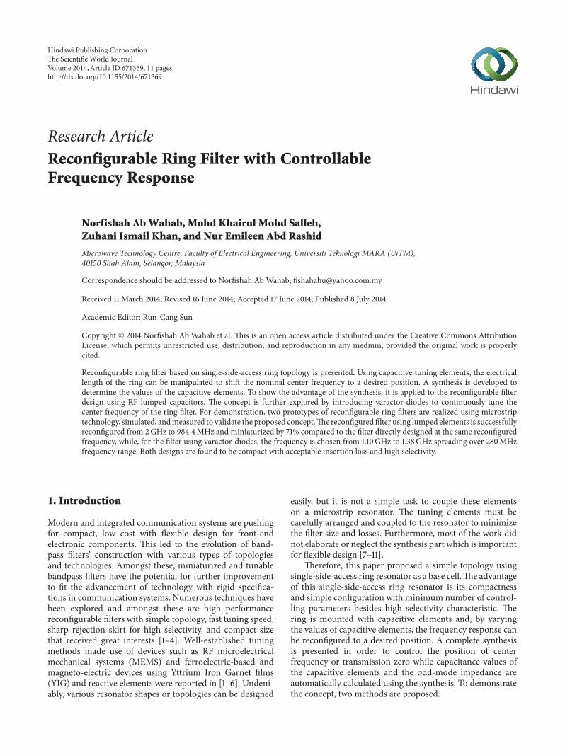
21 Equivalent Circuit and Synthesis Applying the definitionsand parameters of a 3-port coupled-line section given by[12ndash14] a simplified circuit diagram of the reconfigured ringresonator is constructed as shown in Figure 2(a)
The definitions of transformer 119879 the unit element 119884ueand the coupling capacitor 119884
119888are given in (1) to (5) to
represent the 3-port coupled-line section while the 3119885119903and
reconfigured capacitor 119862119903represent the ring lines and the
tuning elements respectively Running a circuit simulation ofthe diagram in Figure 2(a) with the same value of impedancesgiven earlier in Figure 1(a) where 119891
119900= 2GHz 119885
119903= 85Ω
119885119900119890= 70Ω 119885
119900119900= 35Ω and 119862
119903= 1 pF will give the same
results as shown in Figure 2(b)
119884ue = 11988411 minus11988412
2
11988411
(1)
119884119888= 119895 tan
120587119891tz2119891119900
11988411 (2)
11988411=(1119885119900119900+ 1119885
119900119890)
2 (3)
11988412=(1119885119900119900minus 1119885
119900119890)
2 (4)
119879 =11988411
11988412
(5)
Next the reconfigured equivalent circuit in Figure 2(a) issimplified forming a quadripole admittancematrix119884
119877 of the
closed-loop while transformer 119879 and admittance 119884119888 at the
outer section are as depicted in Figure 3At this stage we need to determine the controlling
parameters that influence the position of transmission zeros
The Scientific World Journal 3
1
Input
32 1 Output
Cr Cr
CrCr
Zr
Zr Zr
1205824
1205824
1205824
1205824
Yc
Yue
T
(a)
Frequency (GHz)
Reconfigured resonance
0
1
Reconfigured transmission
05
S11
S12
fo = 2GHz
minus10
minus20
minus30
minus40
frequency for
S-pa
ram
eter
s (dB
)
zero ftzr
(b)
Figure 2 (a) Equivalent circuit diagram of a reconfigurable ring resonator and (b) reconfigured frequency response
and the characteristic performance of the nominal ringTherefore the quadripole admittance matrix of the closed-loop for the nominal ring is termed as matrix 119884 and can bewritten as follows
119884 = [11988411
11988412
11988412
11988411
]
11988411=(4 cos (120579)2 minus 3 + 4119884ue119885119903 cos (120579)
2
minus 119884ue119885119903) cos 120579
119895119885119903sin 120579 (4 cos (120579)2 minus 1)
11988412= minus
1 + 4119861119884ue119885119903cos (120579)3
minus 119861119884ue119885119903 cos 120579(4cos (120579)2 minus 1) 119895119885
119903sin 120579
(6)
with a term given as follows
119861 =(tan (120579)2 + 1)
radic1 + tan (120579)2 (7)
Hence the position of nominal transmission zero 119891tz can bedetermined by equating the 119884
12= 0 resulting in
1 + 4119862119884ue119885119903cos (120579)3
minus 119862119884ue119885119903 cos 120579 = 0 (8)
Next the electrical length of the nominal transmission zeroat the lower side can be expressed as follows
120579tz = arccos(radic1 minus 119884ue1198851199031 + 119884ue119885119903
) (9)
Similarly the electrical length of the nominal transmissionzero can also be represented as
120579tz =120587119891tz2119891119900
(10)
1
Input
32
1 OutputTYC
YR
Figure 3 Simplified reconfigured equivalent circuit diagram with aquadripole admittance matrix 119884
119877
Therefore applying (10) and (11) and for a given nominaltransmission zero frequency119891tz the admittance unit element119884ue can also be written as
119884ue = minus1
(minus1 + 4 cos ((12) (120587119891tz119891119900))2
)119885119903
(11)
Finally 119885119900119900can be written as
119885119900119900= 119885119900119890(2119885119900119890minus 119884ue
119884ue) (12)
At this stage the nominal ring can be constructed at arbitrarycenter frequency119891
119900 with a chosen set of impedance values of
119885119903and 119885
119900119890 while 119885
119900119900is calculated using (12) The next step
is to synthesize the ring circuit with reconfigured capacitor119862119903 shunted at the four edges of the ring line The purpose
of this procedure is to determine the reconfigured frequencyresponse and at the same time calculate the required valuesof capacitor 119862
119903 using the synthesis
Next we need to identify the controlling parameters thatinfluence the shifting of the frequency By solving the matrixelements of the middle quadripole admittance matrix 119884
119877 of
the reconfigurable ring circuit in Figure 3 one can express interms of ABCD-matrix the circuit as follows
119884119877= [
11988411119903
11988412119903
11988412119903
11988411119903
] (13)
4 The Scientific World Journal
12 07 16Frequency (GHz)
0
minus20
minus40
minus60
minus80884MHz
922MHz955MHz
Cr = 304pFCr = 270pF
Cr = 243pF
S-pa
ram
eter
s-S 1
2(d
B)
(a)
07 14Frequency (GHz)
0
1209
minus20
minus40
Cr = 304pFCr = 270pFCr = 243pF
1132GHz 629dB
1178GHz 703dB
1220GHz 772dB
S-pa
ram
eter
s-S 1
1(d
B)
(b)
Figure 4 Frequency responses for three different positions of transmission zeros 119891tz119903 and capacitor 119862119903 is automatically calculated using
the synthesis (a) 11987812and (b) 119878
11
Table 1 Simulated response of a reconfigurable ring resonator designed at center frequency 119891119900= 2GHz with the value of impedances given
by 119885119903= 85Ω 119885
119900119890= 70Ω and 119885
119900119900= 35Ω
Initial setting of reconfiguredtransmission zero 119891tzr1 (GHz) Calculated 119862
119903(pF) Simulated reconfigured responses
Transmission zero 119891tzr2 (GHz) 119891119900119903(GHz)
100 243 0955 12200900 270 0922 11780800 304 0884 1132
Then by solving the quadripole admittance matrix 119884119877 the
reconfigured capacitor 119862119903 can be deduced This is achieved
by equating 11988412119903
= 0
11988412119903
= 4119885119903
2
1205872
119891tz1199032
119862119903
2
119876minus1
(1 minus cos (120579)2)
minus 119875 cos (120579) + 119876minus1 (4119885119903
2
1205872
119891tz1199032
119862119903
2
+ 1)
+ 44119885119903
2
1205872
119891tz1199032
119862119903
2(12) sin (120579)2 cos (120579)2 = 0
(14)
Finally by manipulating (14) it leads to the determination ofreconfigured capacitor119862
119903 which can be expressed as follows
119862119903= minus
119876cos (120579)2 + 119875 cos (120579) minus 119876 minus 2119876119885119903120587119891tz119903 cos (120579) sin (120579)
119876119885119903
2
1205872119891tz1199032 sin (120579)2
(15)
And introducing the terms below to simplify the aboveequation
119875 = radic1 + tan (120579)2
119876 = minus1
minus1 + 4 cos ((12) (120587119891tz1198910))2
(16)
This also means that by fixing the lower side of nominaltransmission zero position119891tz the impedances can be chosen
arbitrarily for a nominal center frequency119891119900 by the designer
one can estimate the value of 119862119903and odd-mode impedance
119885119900119900
which is calculated automatically by (15) and (12)respectively with respect to the position of reconfiguredtransmission zero 119891tz119903
22 Application of Synthesis to Control the Position of Trans-mission Zero An example of reconfigurable ring filter isdesigned with a chosen set of impedances given as follows119885119903
= 85Ω and 119885119900119890
= 70Ω and given by (12) 119885119900119900
is equal to 35 Ω at a nominal center frequency of 2GHzand transmission zero frequency 119891tz at 16 GHz In thissimulation the synthesis is applied and the reconfiguredtransmission zero 119891tz1199031 is set at three different positionswhich are 1 GHz 09GHz and 08GHz Based on 119891tz1199031 thevalues of the capacitors119862
119903 are automatically calculated using
(15)Figures 4(a) and 4(b) depict the frequency responses for
three different sets of reconfigured transmission zero Withapplication of the synthesis different position of reconfiguredtransmission zero gives different value of 119862
119903 The lower the
position of transmission zero is the higher the 119862119903value will
beTable 1 summarized the values of initial setting of recon-
figured transmission zero frequency 119891tz1199031 calculated capaci-tor119862119903 and simulated reconfigured responses of transmission
zero frequency 119891tz1199032 and reconfigured center frequency
The Scientific World Journal 5
Table 2 Summary of values with adjustment impedances 119885119903= 80Ω and 119885
119900119890= 75Ω while 119885
119900119900is automatically calculated to be equal to
35066Ω
Return loss beforeadjustment (dB) Return loss after adjustment (dB) Position of simulated reconfigured center frequency 119891
119900119903
Before adjustment (GHz) After adjustment (GHz)772 dB 3438 dB 1220 1202703 dB 2508 dB 1178 1160629 dB 1997 dB 1132 1114
07 18Frequency (GHz)
0
1209 14 16
Before impedance matchingAfter impedance matching
minus20
minus40
minus60
minus80
Cr = 304pFCr = 270pFCr = 243pF
S-pa
ram
eter
s-S 1
1(d
B)
Figure 5 Comparison of frequency responses between initial andafter impedances modification for 119878
11
119891119900119903 It can be observed that the simulated reconfigured
transmission zeros119891tz1199032 are not at the same positionwith theinitial setting of reconfigured transmission zeros 119891tz1199031 Thisis due to the fact that as the frequency shifted to the left thenominal bandwidth is not conserved anymore Therefore itis easier and more advantageous to control the reconfiguredcenter frequency than the transmission zeros
It can also be observed that the shifting of frequenciesis accompanied by in-band matching problem Thereforeone needs to be cautious in handling the losses duringthe implementation stage with some adjustment needed tobe done on the impedance values of the ring Figure 5illustrates the performance of return loss before and after theadjustment of impedances 119885
119903and 119885
119900119890 It can be seen that
the return loss has improved exceeding 19 dB when both 119885119903
and 119885119900119890are adjusted for impedance matching as compared
to the earlier response in Figure 4 However one has to takenote that with a different set of impedances the positionof center frequency may change accordingly Finally returnloss and center frequencies before and after adjustments aresummarized in Table 2
23 Tuning and Application of Synthesis In a tunable schemeit is an advantage if one can determine the position ofreconfigured center frequency 119891
119900119903 To achieve this theory of
Frequency (GHz)Nominal
frequencyReconfigured center
frequency
BWS-pa
ram
eter
s (dB
)
BWr
for ftz foftzr fo + (fo minus ftz)
Figure 6 Bandwidth of the nominal and reconfigured filter
relative bandwidth (RBW) is applied here in a function ofnominal center frequency 119891
119900 and transmission zero 119891tz
RBW =BW119891119900
=2 (119891119900minus 119891tz)
119891119900
(17)
where BW is bandwidth of the nominal filterUsing relative bandwidth (RBW) concept in (17) relative
bandwidth of reconfigured filter RBW119903 can be written as
follows
RBW119903=BW119903
119891119900119903
= 2(119891119900119903minus 119891tz119903119891119900119903
) (18)
whereby BW119903is bandwidth of reconfigured filter with BW gt
BW119903as illustrated in Figure 6
Therefore to estimate the position of reconfigured centerfrequency 119891
119900119903 an assumption has to be made on the recon-
figured relative bandwidth RBW119903 For calculation purpose
let us assume that the relative bandwidth RBW is alwaysconsistent at any arbitrary center frequency119891
119900Therefore the
reconfigured relative bandwidth RBW119903 can be assumed to be
approximately equal to relative bandwidth of nominal filter asfollows RBW
119903asymp RBW
By using the expressions in (17) and (18) this can bewritten as follows
RBW119903asymp RBW 997904rArr 2119891
119900
(119891119900minus 119891tz)
119891119900
asymp 2119891119900119903(119891119900119903minus 119891tz119903119891119900119903
)
(19)
6 The Scientific World Journal
03 10
0
0705Frequency (GHz)
x = 1 Cr = 3527pF
x = 0805 Cr = 3328pF
minus20
minus40
minus60
minus80
S-pa
ram
eter
s (dB
)
Figure 7 Application of synthesis frequency responses
Hence by manipulating (19) the reconfigured center fre-quency 119891
119900119903 can be equated as follows
119891119900119903asymp2119891tz119903119891119900119891tz
(20)
Taking into account the reconfigured relative bandwidthRBW119903 is only an approximationwhich is assumed to be equal
to the relative bandwidth RBWTherefore to compensate theapproximation and obtain a symmetrical response 119891
119900119903has to
be factorized with a tuning parameter of 119909 In other words(20) can now be written as follows
119891119900119903asymp 2(
119891tz119903119891119900119891tz
)119909 (21)
Somehow to have a good control on filter design it ispractical for the designer to be able to set the position ofreconfigured center frequency 119891
119900119903 Therefore we introduced
a term 119877119900119888 as a ratio of reconfigured center frequency 119891
119900119903
and nominal center frequency 119891119900 and this can be expressed
as follows
119877119900119888=119891119900119903
119891119900
(22)
Finally we can apply the synthesis and predetermine the posi-tion of reconfigured center frequency 119891
119900119903 with initial tuning
parameter 119909 is assumed to be 1 Example of application ofthe synthesis is simulated with a chosen set of impedancesgiven by 119885
119903= 85Ω and 119885
119900119890= 70Ω and given by (12)
119885119900119900
is equal to 35Ω designed at center frequency 119891119900 of
1 GHz Capacitor 119862119903 is automatically calculated using (15) to
be equal to 3527 pF The nominal position of transmissionzero 119891tz is fixed at 083GHz while tuning parameter 119909 istuned accordingly to obtain a symmetrical response Theresponses according to variation of 119909 are depicted in Figure 7and summarized in Table 3 It can be seen that at initial valueof tuning parameter 119909 = 1 the reconfigured center frequencyfalls at 668MHz while the passband responses exhibit poor
Table 3 Summarized values for reconfigured ring designed atnominal center frequency 119891
119900= 1GHz nominal transmission zero
119891tz = 083GHz and 119877oc = 070
Parameter 119909 100 0805119885119903 119885119900119900(Ω) 8500 3500 7500 3462
119885119900119890(Ω) 70 70
Reconfigured centerfrequency 119891
119900119903(GHz) 0668 0700
Calculated 119862119903(pF) 353 3328
Table 4 Summary of frequency responses on ideal circuit designedat 2GHz 119877oc = 05
119909 = 1 119909 = 13
Simulated 119891119900119903
0871 GHz 0984GHz119885119903 119885119900119890 119885119900119900(Ω) 85 70 35 99 92 32
Calculated 119862119903
252 pF 275 pF
matching level When tuning parameter 119909 is tuned to 0805the center frequency is reconfigured to 07GHz To improvethe matching level the impedances are modified as followsby fixing 119885
119900119890 119885119903is modified to 75Ω while 119885
119900119900is recalculated
using (12) and equal to 3462Ω while the value of capacitor119862119903 is given by (15) to be equal to 3328 pF
3 1st Design Using Lumped Capacitors
For demonstration a ring filter using four RF lumped capac-itors as tuning element to reconfigure its center frequencyis proposed The circuit is designed at 119891
119900= 2GHz with
transmission zero119891tz fixed at 16 GHzwhile the reconfiguredcenter frequency 119891
119900119903 is set at 1 GHz The impedances of the
ring resonator are given with values of 119885119903= 85Ω and 119885
119900119890=
70Ω and 119885119900119900
given by (12) equals 35 Ω while capacitor 119862119903
is given by (15) to be equal to 252 pF At initial stage let ussimulate the ideal circuit with parameters set as follows 119909 = 1and 119877
119900119888= 05 As shown in Figure 8 the frequency response
shifted to the left with lower- and upper-side transmissionzeros which are found at 675MHz and 948MHz respectivelywhile the reconfigured center frequency 119891
119900119888 is found at
0871 GHz with attenuation of 293 dB levelHowever this ideal circuit must be tuned to obtain the
position of reconfigured center frequency 119891119900119903 at 1 GHz
This can be achieved by tuning parameter 119909 from 1 to 13For impedance matching 119885
119903is modified to 99Ω 119885
119900119890is
equal to 92Ω and 119885119900119900
is automatically calculated using(12) to be equal to 32Ω while capacitor 119862
119903is given by
(15) to be equal to 275 pF As observed in Figure 8 theposition of reconfigured center frequency 119891
119900119903 is shifted to
0984GHzwith attenuation level improved to be 1737 dBThemodified lower- and upper-side transmission zeros are foundat 780MHz and 1103GHz respectively Table 4 summarizedthe reconfigured center frequencies and capacitance valuesaccording to tuning parameter 119909 The calculated 119862
119903is used
The Scientific World Journal 7
0
05 14 Frequency (GHz)
minus20
minus40
minus60
minus80
S 12-p
aram
eter
s (dB
)
x = 1 Cr = 252pF
x = 13 Cr = 275pF
fo = 10
(a)
Frequency (GHz)
0
07 12
S 11-p
aram
eter
s (dB
)
x = 1 Cr = 252pF
x = 13 Cr = 275pF
minus20
minus40fo = 10
(b)
Figure 8 Simulated frequency responses of the reconfigurable ring resonator on ideal circuit using RF lumped capacitors designed at 2GHz119891tz = 16GHz with 119877
119900119888= 05
Ground Ground
Ground
Ground
RF inRF out
L1
L2
Wr
Wc s
(a) (b)
Figure 9 (a) Final layout of the reconfigurable ring bandpass filter (b) fabricated photo
as an estimation to choose a suitable value of the capacitorfor the implementation of reconfigurable filter on microstripsubstrate
31 Implementation and Results During implementation ofthe filter on microstrip substrate once again the value of thereconfigured capacitor 119862
119903needs to be adjusted This is due
to the effect of connecting pads (to connect the four lumpedcapacitors to the ring resonator) via holes bonding wiressoldering and the availability of the RF lumped capacitorvalue available in the market Based on the calculation of119862119903in the previous discussion RF lumped capacitor with
22 pF is chosen The final layout of the circuit is illustratedin Figure 9(a) with dimensions tabulated in Table 5
The circuit is then implemented using microstrip tech-nology on substrate Tachonic with characteristics given by120576119903= 45 ℎ = 163mm and tan 120575 = 00035 As proved by
work a picture of fabricated reconfigurable ring filter is put
Table 5 Dimensions of the reconfigurable ring filter on Tachonic
Length1198711
(mm)
Length1198712(mm)
Ring width119882119903(mm)
Coupling width119882119888(mm)
Coupling gap119904 (mm)
2400 1895 227 190 040
on view as shown in Figure 9(b) with dimensions tabulatedin Table 5
The simulated and measured frequency responses aredepicted in Figures 10(a) and 10(b) respectively As observedthe simulated reconfigured center frequency attenuates at0985GHz with return loss of 1672 dB and insertion loss of205 dB Two transmissions zeros are found at 921MHz and109GHz with fractional bandwidth of 173 The measure-ment results show that the reconfigured center frequency fallsat 0984GHz and attenuates at 2078 dB level with insertionloss about 3 dB while the two transmission zeros are found
8 The Scientific World Journal
Simulated responseMeasured response
08 12
0
Frequency (GHz)
minus10
minus20
minus30
minus40
minus50
minus60
S 12-p
aram
eter
s (dB
)
(a)
Frequency (GHz)
0
08 12
minus10
minus20
minus30
minus40
minus50
S 11-p
aram
eter
s (dB
)
Simulated responseMeasured response
(b)
Figure 10 Final responses on microstrip for reconfigurable filter using four capacitors (a) simulated and measured 11987811 (b) simulated and
measured 11987812
(a) (b)
Figure 11 Comparison between filters (a) reconfigurable ring filter designed at 2GHz and (b) single mode directly designed at 1 GHz
Table 6 Dimensions of the two filters on Tachonic
Ring filter 119891119900(MHz) Insertion loss (dB) Length (um) Width (um) Total dimension (um2)
Reconfigured at 1 GHz 9844 300 6504 3005 195430Directly designed at 1 GHz 9900 187 12294 5464 671717
at 9494MHz and 1104GHz with fractional bandwidth of203
Finally the reconfigurable filter is compared in terms ofsize with ring filter directly designed at 1 GHz As illustratedin Figures 11(a) and 11(b) the size of reconfigurable ring filteris greatly reduced and miniaturization has been achieved upto 71 compared to the ring filter directly designed at 1 GHzThe dimensions of the two filters are summarized in Table 6
4 2nd Design Using Varactor-Diodes
The reconfigurable filter of the ring resonator is furtherexplored for tunable filter application using four varactor-diodes to electronically and continuously tune the centerfrequency Each varactor-diode is mounted on themicrostripring resonator circuit via biasing circuit which consists of RF
choke resistor 119877dc and DC block capacitor 119862dc DC biasedvoltage is applied to every diode via the resistor 119877dc Thusthe 119877dc has to be large enough to minimize signal leakageSubsequently the capacitor 119862dc has to be sufficient enoughto function as DC block to block the DC bias from flowing tothe resonator Finally every biasing circuit is designed withresistor 119877dc equal to 20 kΩ and capacitor 119862dc equal to 1 nFThe varactors are grounded via hole by drilling themicrostripsubstrate and the connections are made from varactors to theground plane using bond wires
41 Implementation and Results For implementation thevaractor-diode model Skyworks SMV1800 is chosen withspecifications given as follows tuning capacitance (119862
119869) =
145 pF package capacitance (119862119875) = 09 pF bulk resistance
The Scientific World Journal 9
RF inRF out
Varactor
Via hole
VaractorVia hole
Varactor
Via hole
Varactor
Via hole
Vdc
Vdc
Vdc
Rdc
Rdc
Rdc Rdc
Cdc
Cdc
Cdc Cdc
Wr
Lr
Lr1
Wcs
+minus
+minus
+minus
(a) (b)
Figure 12 (a) Layout of the electronically reconfigurable ring bandpass filter using four Skyworks SMV 1800 varactors for impedances119885119903= 80Ω 119885
119900119890= 75Ω and 119885
119900119900= 30Ω (b) photo of fabricated filter
Table 7 Dimensions of ring filter designed at 2GHz and biasing components
Length 119871119903(mm) Length 119871
1199031(mm) Coupling width119882
119888(mm) Width ring119882
119903(mm) Gap s (mm) 119877dc (kΩ) 119862dc (nF)
2250 2020 230 140 024 2000 100
Table 8 Measured responses of reconfigurable ring filter designed at 2GHz
DC supply voltage Poles (GHz) Transmission zeros (GHz) Insertion loss (dB) Return loss (dB) FBW 10 volt 110 096 123 312 2896 930 volt 138 119 160 156 1862 10
(119877119878) = 25 ohm and package inductance (119871
119878) = 08 nH
[15]This model is chosen because of the range of capacitanceeffect of the varactor which is sufficient to tune the filterfrom 2GHz to a desired minimum center frequency of 1 GHz(using (15) 119862
119903is approximately equal to 2 pF)
The electronically reconfigurable circuit is designed at2GHz with a chosen set of impedances given by 119885
119903= 80Ω
119885119900119890= 75Ω and 119885
119900119900= 30Ω The proposed reconfigurable
ring bandpass filter is designed using four varactors with bias-ing circuits which are loaded at the edge of the ring resonatorto create capacitance effect to the ring resonator The circuitis implemented using microstrip technology and substrateTachonic with characteristics given by 120576
119903= 45 ℎ = 163mm
and tan 120575 = 00035 The final layout of the filter is depictedin Figure 12(a) with dimensions summarized in Table 7 and apicture of the prototype microstrip reconfigurable bandpassfilter is shown in Figure 12(b) as proved by work
For a successful reconfigurable filter design there hasto be a trade-off between tunability dynamic range andloss to ensure high filter performance Therefore acceptablelevels of the frequency responses are chosen in the rangefrom 10V to 30V only From the simulation it shows thatwhen DC bias voltage is at 10V the insertion loss is 289 dBand the return loss is 2249 dB found at 109GHz Thetwo transmission zeros exist at 986MHz and 117 GHz with
fractional bandwidth of 4 When DC bias voltage is at 30Vthe center frequency is found at 137GHz with insertionloss at 105 dB and return loss at 2398 dB Two transmissionzeros are obtained at 122GHz and 151 GHz respectivelygiving a fractional bandwidth of 5The simulated frequencyresponses are illustrated in Figures 13(a) and 13(b)
The measured results are shown in Figures 14(a) and14(b) The passband characteristics have an insertion lossof 312 dB and return loss of 2896 at 110GHz when theforward bias is at 10V Two transmission zeros are obtainedat 960MHz and 123GHz respectively with fractional band-width of 9 At forward bias of 30V the insertion loss is156 dB while the return loss is 1862 dB at 138GHz Twotransmission zeros are obtained at 119 GHz and 160GHzwith fractional bandwidth of 10
In general it is difficult to control both frequencyresponses and bandwidths along the tuning range Assummarized in Table 8 the measured fractional bandwidth(FBW) is about 10 which is doubled as compared tothe simulated FBW in Figure 13 Some possible techniquesfor better control of bandwidth such as coupling of thenonresonant transmission line of the filter could be employedfor future improvement [16] In terms of tunability the centerfrequencies are spreading over 280MHz which gives 25achievable tuning range while the insertion losses from 30V
10 The Scientific World Journal
12
0
1410 1609Frequency (GHz)
minus20
minus40
10 volts14 volts18 volts 22 volts
26 volts30 volts
S-pa
ram
eter
s (dB
) (S 1
2)
(a)
12
0
1410 16Frequency (GHz)
minus20
minus40
10 volts
14 volts
18 volts
22 volts26 volts
30 volts
S-pa
ram
eter
s (dB
) (S 1
1)
(b)
Figure 13 Tuning range from 10V to 30V of the electronically bandpass filter for (a) simulated 11987812and (b) simulated 119878
11
10Frequency (GHz)
0
1812 14 1608
10 volts14 volts
18 volts 22 volts26 volts30 volts
S-pa
ram
eter
s (dB
) (S 1
2) minus10
minus20
minus30
minus40
minus50
(a)
Frequency (GHz)
0
1810 12 14 16
10 volts14 volts
18 volts22 volts26 volts
30 volts
minus20
minus40
S-pa
ram
eter
s (dB
) (S 1
1)
(b)
Figure 14 Measured frequency responses for tuning range from 10V to 30V (a) 11987812and (b) 119878
11
to 10V are in the range of 156 dB to 312 dB which are withinthe acceptable specification As can be observed there aredifferences between the simulated and measured insertionlosses This can be attributed to tolerances in the componentvalues and fabrication process
5 Conclusion
This paper explored the use of ring-based resonator topologyto develop reconfigurable ring filters This study had proventhat the nominal center frequency of the ring filter can betuned by introducing capacitive elements which had createdvariation of electrical length to the ring lines Synthesis waspresented to control the position of reconfigurable centerfrequency or transmission zero while the value of capacitiveelements and the odd-mode impedance are automatically
calculated For demonstration two reconfigurable filters wereproposed using two different tuning techniques The firstprototype made use of four lumped capacitors and thenominal center frequencywas successfully reconfigured from2GHz to 9844MHz with narrow fractional bandwidth of203 In terms of size this filter was successfully reducedby 71 compared to the filter designed directly at 1 GHzThe second prototype made use of hyperabrupt junctionvaractor-diodes Skywork SMV1800 and the nominal centerfrequency was tuned in the chosen range of 110GHz to138GHz spreading over 280MHz frequency range withachievable tuning range of 25 and fractional bandwidthbelow 10 The frequency responses for both filters hadshown good passband response high selectivity with twofinite transmission zeros and narrow bandwidth throughoutthe tuning range Finally both prototypes were simulated andmeasured to validate the concept
The Scientific World Journal 11
Conflict of Interests
The authors declare that there is no conflict of interestsregarding the publication of this paper
Acknowledgment
The authors would like to thank Ministry of EducationMalaysia and Research Management Institute (RMI) Uni-versiti Teknologi MARA with Grant no 600-RMI-NRGS53(32013) for funding this project
References
[1] R Saal and E Ulbrich ldquoOn the design of filters by synthesisrdquoIRE Transactions on Circuit Theory vol 5 pp 284ndash327 1958
[2] G Matthaei L Young and E M T Jones MicrowaveImpedance-Matching Networks and Coupling Structures ArtechHouse Norwood Mass USA 1985
[3] I C Hunter and J D Rhodes ldquoElectronically tuneablemicrowave bandpass filtersrdquo IEEE Transactions on MicrowaveTheory and Techniques vol 30 no 9 pp 135ndash136 1982
[4] J Long C Li W Cui J Huangfu and L Ran ldquoA tunablemicrostrip bandpass filter with two independently adjustabletransmission zerosrdquo IEEE Microwave and Wireless ComponentsLetters vol 21 no 2 pp 74ndash76 2011
[5] S W Fok P Cheong K W Tam and R P Martins ldquoA novelmicrostrip square-loop dual-mode bandpass filter with simulta-neous size reduction and spurious response suppressionrdquo IEEETransactions on Microwave Theory and Techniques vol 54 no5 pp 2033ndash2040 2006
[6] S L Delprat J Oh F Xu et al ldquoFully distributed tunablebandpass filter based on Ba
05Sr05TiO3thin-film slow-wave
structurerdquo International Journal of Microwave Science andTechnology vol 2011 Article ID 468074 9 pages 2011
[7] Y Chiou and G M Rebeiz ldquoTunable 155ndash21 GHz 4-poleelliptic bandpass filter with bandwidth control and gt50 dBrejection for wireless systemsrdquo IEEE Transactions onMicrowaveTheory and Techniques vol 61 no 1 pp 117ndash124 2013
[8] R Mao X Tang and F Xiao ldquoMiniaturized dual-mode ringbandpass filters with patterned ground planerdquo IEEE Transac-tions on Microwave Theory and Techniques vol 55 no 7 pp1539ndash1546 2007
[9] A Miller and J-S Hong ldquoReconfigurable cascaded coupledline filter with four distinct bandwidth statesrdquo IET MicrowavesAntennas and Propagation vol 5 no 14 pp 1730ndash1737 2011
[10] H-WHsu C-H Lai and T-GMa ldquoAminiaturized dual-modering bandpass filterrdquo IEEEMicrowave andWireless ComponentsLetters vol 20 no 10 pp 542ndash544 2010
[11] MA El-Tanani andGMRebeiz ldquoA two-pole two-zero tunablefilter with improved linearityrdquo IEEE Transactions on MicrowaveTheory and Techniques vol 57 no 4 pp 830ndash839 2009
[12] H Ozaki and J Ishii ldquoSynthesis of a class of strip-line filtersrdquoIRE Transactions on Circuit Theory vol 5 no 2 pp 104ndash1091958
[13] Y Nemoto K Kobayashi and R Sato ldquoGraph transformationsof nonuniform coupled transmission line networks and theirapplicationrdquo IEEE Transactions on MicrowaveTheory and Tech-niques vol 33 no 11 pp 1257ndash1263 1985
[14] R Sato and E G Cristal ldquoSimplified analysis of cou-pled transmission-line networks and their application (Short
Paper)rdquo IEEE Transactions on Microwave Theory and Tech-niques vol 18 no 3 pp 122ndash132 1970
[15] Skyworks Solution Datasheet for SMV-1232 httpwwwsky-worksinccomfor SMV-1232
[16] N Zahirovic S Fouladi R R Mansour and M Yu ldquoTunablesuspended substrate stripline filters with constant bandwidthrdquoin Proceedings of the IEEE MTT-S International MicrowaveSymposium (IMS rsquo11) June 2011
International Journal of
AerospaceEngineeringHindawi Publishing Corporationhttpwwwhindawicom Volume 2014
RoboticsJournal of
Hindawi Publishing Corporationhttpwwwhindawicom Volume 2014
Hindawi Publishing Corporationhttpwwwhindawicom Volume 2014
Active and Passive Electronic Components
Control Scienceand Engineering
Journal of
Hindawi Publishing Corporationhttpwwwhindawicom Volume 2014
International Journal of
RotatingMachinery
Hindawi Publishing Corporationhttpwwwhindawicom Volume 2014
Hindawi Publishing Corporation httpwwwhindawicom
Journal ofEngineeringVolume 2014
Submit your manuscripts athttpwwwhindawicom
VLSI Design
Hindawi Publishing Corporationhttpwwwhindawicom Volume 2014
Hindawi Publishing Corporationhttpwwwhindawicom Volume 2014
Shock and Vibration
Hindawi Publishing Corporationhttpwwwhindawicom Volume 2014
Civil EngineeringAdvances in
Acoustics and VibrationAdvances in
Hindawi Publishing Corporationhttpwwwhindawicom Volume 2014
Hindawi Publishing Corporationhttpwwwhindawicom Volume 2014
Electrical and Computer Engineering
Journal of
Advances inOptoElectronics
Hindawi Publishing Corporation httpwwwhindawicom
Volume 2014
The Scientific World JournalHindawi Publishing Corporation httpwwwhindawicom Volume 2014
SensorsJournal of
Hindawi Publishing Corporationhttpwwwhindawicom Volume 2014
Modelling amp Simulation in EngineeringHindawi Publishing Corporation httpwwwhindawicom Volume 2014
Hindawi Publishing Corporationhttpwwwhindawicom Volume 2014
Chemical EngineeringInternational Journal of Antennas and
Propagation
International Journal of
Hindawi Publishing Corporationhttpwwwhindawicom Volume 2014
Hindawi Publishing Corporationhttpwwwhindawicom Volume 2014
Navigation and Observation
International Journal of
Hindawi Publishing Corporationhttpwwwhindawicom Volume 2014
DistributedSensor Networks
International Journal of

2 The Scientific World Journal
Cr Cr
Cr
Cr
Zr
Zr
Zrlr
lr
lr
Zoe Zoo
(a)
Frequency (GHz)
Nominalresponse
Shifted response
0
minus10
minus20
minus30
minus40
minus50
S11S12
fominusx fo = 2GHz
S-pa
ram
eter
s (dB
)
(b)
Figure 1 Reconfigurable ring filter electrical length 119897119903 and four shunted capacitors designed at center frequency 119891
119900= 2GHz for 119885
119903= 85Ω
119885119900119890= 70Ω 119885
119900119900= 35Ω and 119862
119903= 1 pF (a) Topology and (b) frequency responses
The first method applies RF lumped capacitors as thetuning element This filter is designed at higher centerfrequency 119891
119900and by varying the value of the capacitor the
nominal center frequency can be shifted to a desired positionwhich is lower than the nominal center frequency at 119891
119900119903 The
advantage of this design is that the position of reconfiguredcenter frequency can be fixed to a desired position whilethe value of the capacitors and the odd-mode impedanceare calculated automatically using the synthesis Impedancematching can be achieved by adjusting the impedance valuesof the ring The filter is miniaturized up to 71 comparedto the ring filter designed directly at the same reconfiguredcenter frequency 119891
119900119903
To further explore the tuning aspect of the reconfigurablefilter varactor-diode with biasing circuit is introduced as thetuning element to electronically tune the center frequencyof the ring filter The advantage of this method is that evenwith a small capacitance values the circuit is capable of tun-ing continuously to create a frequency-agile characteristicFinally both designs are realized on microstrip substratessimulated and measured using EM solvers to demonstratethe idea
2 Design of Reconfigurable Ring Filter
A ring resonator is shunted with four capacitive elements119862119903
at the edges of the ring lines to vary the nominal electricallength 119897
119903 of the ring The variation of electrical length
depends on the variation values of 119862119903to reconfigure the
nominal center frequency to a new position As shown inFigure 1(a) the ring is reconfigured with a set of chosenimpedances as follows ring impedance 119885
119903= 85Ω even-
mode impedance 119885119900119890= 70Ω and odd-mode impedance
119885119900119900= 35Ω while the tuning element known as reconfigured
capacitor 119862119903 is chosen to be equal to 1 pF Figure 1(b) illus-
trates the frequency responses between the reconfigured ringand the nominal ring without the four reactive elements Asobserved the nominal center frequency 119891
119900 is reconfigured
to the left at 119891119900-119909 due to the changes in electrical length of the
ring lines
21 Equivalent Circuit and Synthesis Applying the definitionsand parameters of a 3-port coupled-line section given by[12ndash14] a simplified circuit diagram of the reconfigured ringresonator is constructed as shown in Figure 2(a)
The definitions of transformer 119879 the unit element 119884ueand the coupling capacitor 119884
119888are given in (1) to (5) to
represent the 3-port coupled-line section while the 3119885119903and
reconfigured capacitor 119862119903represent the ring lines and the
tuning elements respectively Running a circuit simulation ofthe diagram in Figure 2(a) with the same value of impedancesgiven earlier in Figure 1(a) where 119891
119900= 2GHz 119885
119903= 85Ω
119885119900119890= 70Ω 119885
119900119900= 35Ω and 119862
119903= 1 pF will give the same
results as shown in Figure 2(b)
119884ue = 11988411 minus11988412
2
11988411
(1)
119884119888= 119895 tan
120587119891tz2119891119900
11988411 (2)
11988411=(1119885119900119900+ 1119885
119900119890)
2 (3)
11988412=(1119885119900119900minus 1119885
119900119890)
2 (4)
119879 =11988411
11988412
(5)
Next the reconfigured equivalent circuit in Figure 2(a) issimplified forming a quadripole admittancematrix119884
119877 of the
closed-loop while transformer 119879 and admittance 119884119888 at the
outer section are as depicted in Figure 3At this stage we need to determine the controlling
parameters that influence the position of transmission zeros
The Scientific World Journal 3
1
Input
32 1 Output
Cr Cr
CrCr
Zr
Zr Zr
1205824
1205824
1205824
1205824
Yc
Yue
T
(a)
Frequency (GHz)
Reconfigured resonance
0
1
Reconfigured transmission
05
S11
S12
fo = 2GHz
minus10
minus20
minus30
minus40
frequency for
S-pa
ram
eter
s (dB
)
zero ftzr
(b)
Figure 2 (a) Equivalent circuit diagram of a reconfigurable ring resonator and (b) reconfigured frequency response
and the characteristic performance of the nominal ringTherefore the quadripole admittance matrix of the closed-loop for the nominal ring is termed as matrix 119884 and can bewritten as follows
119884 = [11988411
11988412
11988412
11988411
]
11988411=(4 cos (120579)2 minus 3 + 4119884ue119885119903 cos (120579)
2
minus 119884ue119885119903) cos 120579
119895119885119903sin 120579 (4 cos (120579)2 minus 1)
11988412= minus
1 + 4119861119884ue119885119903cos (120579)3
minus 119861119884ue119885119903 cos 120579(4cos (120579)2 minus 1) 119895119885
119903sin 120579
(6)
with a term given as follows
119861 =(tan (120579)2 + 1)
radic1 + tan (120579)2 (7)
Hence the position of nominal transmission zero 119891tz can bedetermined by equating the 119884
12= 0 resulting in
1 + 4119862119884ue119885119903cos (120579)3
minus 119862119884ue119885119903 cos 120579 = 0 (8)
Next the electrical length of the nominal transmission zeroat the lower side can be expressed as follows
120579tz = arccos(radic1 minus 119884ue1198851199031 + 119884ue119885119903
) (9)
Similarly the electrical length of the nominal transmissionzero can also be represented as
120579tz =120587119891tz2119891119900
(10)
1
Input
32
1 OutputTYC
YR
Figure 3 Simplified reconfigured equivalent circuit diagram with aquadripole admittance matrix 119884
119877
Therefore applying (10) and (11) and for a given nominaltransmission zero frequency119891tz the admittance unit element119884ue can also be written as
119884ue = minus1
(minus1 + 4 cos ((12) (120587119891tz119891119900))2
)119885119903
(11)
Finally 119885119900119900can be written as
119885119900119900= 119885119900119890(2119885119900119890minus 119884ue
119884ue) (12)
At this stage the nominal ring can be constructed at arbitrarycenter frequency119891
119900 with a chosen set of impedance values of
119885119903and 119885
119900119890 while 119885
119900119900is calculated using (12) The next step
is to synthesize the ring circuit with reconfigured capacitor119862119903 shunted at the four edges of the ring line The purpose
of this procedure is to determine the reconfigured frequencyresponse and at the same time calculate the required valuesof capacitor 119862
119903 using the synthesis
Next we need to identify the controlling parameters thatinfluence the shifting of the frequency By solving the matrixelements of the middle quadripole admittance matrix 119884
119877 of
the reconfigurable ring circuit in Figure 3 one can express interms of ABCD-matrix the circuit as follows
119884119877= [
11988411119903
11988412119903
11988412119903
11988411119903
] (13)
4 The Scientific World Journal
12 07 16Frequency (GHz)
0
minus20
minus40
minus60
minus80884MHz
922MHz955MHz
Cr = 304pFCr = 270pF
Cr = 243pF
S-pa
ram
eter
s-S 1
2(d
B)
(a)
07 14Frequency (GHz)
0
1209
minus20
minus40
Cr = 304pFCr = 270pFCr = 243pF
1132GHz 629dB
1178GHz 703dB
1220GHz 772dB
S-pa
ram
eter
s-S 1
1(d
B)
(b)
Figure 4 Frequency responses for three different positions of transmission zeros 119891tz119903 and capacitor 119862119903 is automatically calculated using
the synthesis (a) 11987812and (b) 119878
11
Table 1 Simulated response of a reconfigurable ring resonator designed at center frequency 119891119900= 2GHz with the value of impedances given
by 119885119903= 85Ω 119885
119900119890= 70Ω and 119885
119900119900= 35Ω
Initial setting of reconfiguredtransmission zero 119891tzr1 (GHz) Calculated 119862
119903(pF) Simulated reconfigured responses
Transmission zero 119891tzr2 (GHz) 119891119900119903(GHz)
100 243 0955 12200900 270 0922 11780800 304 0884 1132
Then by solving the quadripole admittance matrix 119884119877 the
reconfigured capacitor 119862119903 can be deduced This is achieved
by equating 11988412119903
= 0
11988412119903
= 4119885119903
2
1205872
119891tz1199032
119862119903
2
119876minus1
(1 minus cos (120579)2)
minus 119875 cos (120579) + 119876minus1 (4119885119903
2
1205872
119891tz1199032
119862119903
2
+ 1)
+ 44119885119903
2
1205872
119891tz1199032
119862119903
2(12) sin (120579)2 cos (120579)2 = 0
(14)
Finally by manipulating (14) it leads to the determination ofreconfigured capacitor119862
119903 which can be expressed as follows
119862119903= minus
119876cos (120579)2 + 119875 cos (120579) minus 119876 minus 2119876119885119903120587119891tz119903 cos (120579) sin (120579)
119876119885119903
2
1205872119891tz1199032 sin (120579)2
(15)
And introducing the terms below to simplify the aboveequation
119875 = radic1 + tan (120579)2
119876 = minus1
minus1 + 4 cos ((12) (120587119891tz1198910))2
(16)
This also means that by fixing the lower side of nominaltransmission zero position119891tz the impedances can be chosen
arbitrarily for a nominal center frequency119891119900 by the designer
one can estimate the value of 119862119903and odd-mode impedance
119885119900119900
which is calculated automatically by (15) and (12)respectively with respect to the position of reconfiguredtransmission zero 119891tz119903
22 Application of Synthesis to Control the Position of Trans-mission Zero An example of reconfigurable ring filter isdesigned with a chosen set of impedances given as follows119885119903
= 85Ω and 119885119900119890
= 70Ω and given by (12) 119885119900119900
is equal to 35 Ω at a nominal center frequency of 2GHzand transmission zero frequency 119891tz at 16 GHz In thissimulation the synthesis is applied and the reconfiguredtransmission zero 119891tz1199031 is set at three different positionswhich are 1 GHz 09GHz and 08GHz Based on 119891tz1199031 thevalues of the capacitors119862
119903 are automatically calculated using
(15)Figures 4(a) and 4(b) depict the frequency responses for
three different sets of reconfigured transmission zero Withapplication of the synthesis different position of reconfiguredtransmission zero gives different value of 119862
119903 The lower the
position of transmission zero is the higher the 119862119903value will
beTable 1 summarized the values of initial setting of recon-
figured transmission zero frequency 119891tz1199031 calculated capaci-tor119862119903 and simulated reconfigured responses of transmission
zero frequency 119891tz1199032 and reconfigured center frequency
The Scientific World Journal 5
Table 2 Summary of values with adjustment impedances 119885119903= 80Ω and 119885
119900119890= 75Ω while 119885
119900119900is automatically calculated to be equal to
35066Ω
Return loss beforeadjustment (dB) Return loss after adjustment (dB) Position of simulated reconfigured center frequency 119891
119900119903
Before adjustment (GHz) After adjustment (GHz)772 dB 3438 dB 1220 1202703 dB 2508 dB 1178 1160629 dB 1997 dB 1132 1114
07 18Frequency (GHz)
0
1209 14 16
Before impedance matchingAfter impedance matching
minus20
minus40
minus60
minus80
Cr = 304pFCr = 270pFCr = 243pF
S-pa
ram
eter
s-S 1
1(d
B)
Figure 5 Comparison of frequency responses between initial andafter impedances modification for 119878
11
119891119900119903 It can be observed that the simulated reconfigured
transmission zeros119891tz1199032 are not at the same positionwith theinitial setting of reconfigured transmission zeros 119891tz1199031 Thisis due to the fact that as the frequency shifted to the left thenominal bandwidth is not conserved anymore Therefore itis easier and more advantageous to control the reconfiguredcenter frequency than the transmission zeros
It can also be observed that the shifting of frequenciesis accompanied by in-band matching problem Thereforeone needs to be cautious in handling the losses duringthe implementation stage with some adjustment needed tobe done on the impedance values of the ring Figure 5illustrates the performance of return loss before and after theadjustment of impedances 119885
119903and 119885
119900119890 It can be seen that
the return loss has improved exceeding 19 dB when both 119885119903
and 119885119900119890are adjusted for impedance matching as compared
to the earlier response in Figure 4 However one has to takenote that with a different set of impedances the positionof center frequency may change accordingly Finally returnloss and center frequencies before and after adjustments aresummarized in Table 2
23 Tuning and Application of Synthesis In a tunable schemeit is an advantage if one can determine the position ofreconfigured center frequency 119891
119900119903 To achieve this theory of
Frequency (GHz)Nominal
frequencyReconfigured center
frequency
BWS-pa
ram
eter
s (dB
)
BWr
for ftz foftzr fo + (fo minus ftz)
Figure 6 Bandwidth of the nominal and reconfigured filter
relative bandwidth (RBW) is applied here in a function ofnominal center frequency 119891
119900 and transmission zero 119891tz
RBW =BW119891119900
=2 (119891119900minus 119891tz)
119891119900
(17)
where BW is bandwidth of the nominal filterUsing relative bandwidth (RBW) concept in (17) relative
bandwidth of reconfigured filter RBW119903 can be written as
follows
RBW119903=BW119903
119891119900119903
= 2(119891119900119903minus 119891tz119903119891119900119903
) (18)
whereby BW119903is bandwidth of reconfigured filter with BW gt
BW119903as illustrated in Figure 6
Therefore to estimate the position of reconfigured centerfrequency 119891
119900119903 an assumption has to be made on the recon-
figured relative bandwidth RBW119903 For calculation purpose
let us assume that the relative bandwidth RBW is alwaysconsistent at any arbitrary center frequency119891
119900Therefore the
reconfigured relative bandwidth RBW119903 can be assumed to be
approximately equal to relative bandwidth of nominal filter asfollows RBW
119903asymp RBW
By using the expressions in (17) and (18) this can bewritten as follows
RBW119903asymp RBW 997904rArr 2119891
119900
(119891119900minus 119891tz)
119891119900
asymp 2119891119900119903(119891119900119903minus 119891tz119903119891119900119903
)
(19)
6 The Scientific World Journal
03 10
0
0705Frequency (GHz)
x = 1 Cr = 3527pF
x = 0805 Cr = 3328pF
minus20
minus40
minus60
minus80
S-pa
ram
eter
s (dB
)
Figure 7 Application of synthesis frequency responses
Hence by manipulating (19) the reconfigured center fre-quency 119891
119900119903 can be equated as follows
119891119900119903asymp2119891tz119903119891119900119891tz
(20)
Taking into account the reconfigured relative bandwidthRBW119903 is only an approximationwhich is assumed to be equal
to the relative bandwidth RBWTherefore to compensate theapproximation and obtain a symmetrical response 119891
119900119903has to
be factorized with a tuning parameter of 119909 In other words(20) can now be written as follows
119891119900119903asymp 2(
119891tz119903119891119900119891tz
)119909 (21)
Somehow to have a good control on filter design it ispractical for the designer to be able to set the position ofreconfigured center frequency 119891
119900119903 Therefore we introduced
a term 119877119900119888 as a ratio of reconfigured center frequency 119891
119900119903
and nominal center frequency 119891119900 and this can be expressed
as follows
119877119900119888=119891119900119903
119891119900
(22)
Finally we can apply the synthesis and predetermine the posi-tion of reconfigured center frequency 119891
119900119903 with initial tuning
parameter 119909 is assumed to be 1 Example of application ofthe synthesis is simulated with a chosen set of impedancesgiven by 119885
119903= 85Ω and 119885
119900119890= 70Ω and given by (12)
119885119900119900
is equal to 35Ω designed at center frequency 119891119900 of
1 GHz Capacitor 119862119903 is automatically calculated using (15) to
be equal to 3527 pF The nominal position of transmissionzero 119891tz is fixed at 083GHz while tuning parameter 119909 istuned accordingly to obtain a symmetrical response Theresponses according to variation of 119909 are depicted in Figure 7and summarized in Table 3 It can be seen that at initial valueof tuning parameter 119909 = 1 the reconfigured center frequencyfalls at 668MHz while the passband responses exhibit poor
Table 3 Summarized values for reconfigured ring designed atnominal center frequency 119891
119900= 1GHz nominal transmission zero
119891tz = 083GHz and 119877oc = 070
Parameter 119909 100 0805119885119903 119885119900119900(Ω) 8500 3500 7500 3462
119885119900119890(Ω) 70 70
Reconfigured centerfrequency 119891
119900119903(GHz) 0668 0700
Calculated 119862119903(pF) 353 3328
Table 4 Summary of frequency responses on ideal circuit designedat 2GHz 119877oc = 05
119909 = 1 119909 = 13
Simulated 119891119900119903
0871 GHz 0984GHz119885119903 119885119900119890 119885119900119900(Ω) 85 70 35 99 92 32
Calculated 119862119903
252 pF 275 pF
matching level When tuning parameter 119909 is tuned to 0805the center frequency is reconfigured to 07GHz To improvethe matching level the impedances are modified as followsby fixing 119885
119900119890 119885119903is modified to 75Ω while 119885
119900119900is recalculated
using (12) and equal to 3462Ω while the value of capacitor119862119903 is given by (15) to be equal to 3328 pF
3 1st Design Using Lumped Capacitors
For demonstration a ring filter using four RF lumped capac-itors as tuning element to reconfigure its center frequencyis proposed The circuit is designed at 119891
119900= 2GHz with
transmission zero119891tz fixed at 16 GHzwhile the reconfiguredcenter frequency 119891
119900119903 is set at 1 GHz The impedances of the
ring resonator are given with values of 119885119903= 85Ω and 119885
119900119890=
70Ω and 119885119900119900
given by (12) equals 35 Ω while capacitor 119862119903
is given by (15) to be equal to 252 pF At initial stage let ussimulate the ideal circuit with parameters set as follows 119909 = 1and 119877
119900119888= 05 As shown in Figure 8 the frequency response
shifted to the left with lower- and upper-side transmissionzeros which are found at 675MHz and 948MHz respectivelywhile the reconfigured center frequency 119891
119900119888 is found at
0871 GHz with attenuation of 293 dB levelHowever this ideal circuit must be tuned to obtain the
position of reconfigured center frequency 119891119900119903 at 1 GHz
This can be achieved by tuning parameter 119909 from 1 to 13For impedance matching 119885
119903is modified to 99Ω 119885
119900119890is
equal to 92Ω and 119885119900119900
is automatically calculated using(12) to be equal to 32Ω while capacitor 119862
119903is given by
(15) to be equal to 275 pF As observed in Figure 8 theposition of reconfigured center frequency 119891
119900119903 is shifted to
0984GHzwith attenuation level improved to be 1737 dBThemodified lower- and upper-side transmission zeros are foundat 780MHz and 1103GHz respectively Table 4 summarizedthe reconfigured center frequencies and capacitance valuesaccording to tuning parameter 119909 The calculated 119862
119903is used
The Scientific World Journal 7
0
05 14 Frequency (GHz)
minus20
minus40
minus60
minus80
S 12-p
aram
eter
s (dB
)
x = 1 Cr = 252pF
x = 13 Cr = 275pF
fo = 10
(a)
Frequency (GHz)
0
07 12
S 11-p
aram
eter
s (dB
)
x = 1 Cr = 252pF
x = 13 Cr = 275pF
minus20
minus40fo = 10
(b)
Figure 8 Simulated frequency responses of the reconfigurable ring resonator on ideal circuit using RF lumped capacitors designed at 2GHz119891tz = 16GHz with 119877
119900119888= 05
Ground Ground
Ground
Ground
RF inRF out
L1
L2
Wr
Wc s
(a) (b)
Figure 9 (a) Final layout of the reconfigurable ring bandpass filter (b) fabricated photo
as an estimation to choose a suitable value of the capacitorfor the implementation of reconfigurable filter on microstripsubstrate
31 Implementation and Results During implementation ofthe filter on microstrip substrate once again the value of thereconfigured capacitor 119862
119903needs to be adjusted This is due
to the effect of connecting pads (to connect the four lumpedcapacitors to the ring resonator) via holes bonding wiressoldering and the availability of the RF lumped capacitorvalue available in the market Based on the calculation of119862119903in the previous discussion RF lumped capacitor with
22 pF is chosen The final layout of the circuit is illustratedin Figure 9(a) with dimensions tabulated in Table 5
The circuit is then implemented using microstrip tech-nology on substrate Tachonic with characteristics given by120576119903= 45 ℎ = 163mm and tan 120575 = 00035 As proved by
work a picture of fabricated reconfigurable ring filter is put
Table 5 Dimensions of the reconfigurable ring filter on Tachonic
Length1198711
(mm)
Length1198712(mm)
Ring width119882119903(mm)
Coupling width119882119888(mm)
Coupling gap119904 (mm)
2400 1895 227 190 040
on view as shown in Figure 9(b) with dimensions tabulatedin Table 5
The simulated and measured frequency responses aredepicted in Figures 10(a) and 10(b) respectively As observedthe simulated reconfigured center frequency attenuates at0985GHz with return loss of 1672 dB and insertion loss of205 dB Two transmissions zeros are found at 921MHz and109GHz with fractional bandwidth of 173 The measure-ment results show that the reconfigured center frequency fallsat 0984GHz and attenuates at 2078 dB level with insertionloss about 3 dB while the two transmission zeros are found
8 The Scientific World Journal
Simulated responseMeasured response
08 12
0
Frequency (GHz)
minus10
minus20
minus30
minus40
minus50
minus60
S 12-p
aram
eter
s (dB
)
(a)
Frequency (GHz)
0
08 12
minus10
minus20
minus30
minus40
minus50
S 11-p
aram
eter
s (dB
)
Simulated responseMeasured response
(b)
Figure 10 Final responses on microstrip for reconfigurable filter using four capacitors (a) simulated and measured 11987811 (b) simulated and
measured 11987812
(a) (b)
Figure 11 Comparison between filters (a) reconfigurable ring filter designed at 2GHz and (b) single mode directly designed at 1 GHz
Table 6 Dimensions of the two filters on Tachonic
Ring filter 119891119900(MHz) Insertion loss (dB) Length (um) Width (um) Total dimension (um2)
Reconfigured at 1 GHz 9844 300 6504 3005 195430Directly designed at 1 GHz 9900 187 12294 5464 671717
at 9494MHz and 1104GHz with fractional bandwidth of203
Finally the reconfigurable filter is compared in terms ofsize with ring filter directly designed at 1 GHz As illustratedin Figures 11(a) and 11(b) the size of reconfigurable ring filteris greatly reduced and miniaturization has been achieved upto 71 compared to the ring filter directly designed at 1 GHzThe dimensions of the two filters are summarized in Table 6
4 2nd Design Using Varactor-Diodes
The reconfigurable filter of the ring resonator is furtherexplored for tunable filter application using four varactor-diodes to electronically and continuously tune the centerfrequency Each varactor-diode is mounted on themicrostripring resonator circuit via biasing circuit which consists of RF
choke resistor 119877dc and DC block capacitor 119862dc DC biasedvoltage is applied to every diode via the resistor 119877dc Thusthe 119877dc has to be large enough to minimize signal leakageSubsequently the capacitor 119862dc has to be sufficient enoughto function as DC block to block the DC bias from flowing tothe resonator Finally every biasing circuit is designed withresistor 119877dc equal to 20 kΩ and capacitor 119862dc equal to 1 nFThe varactors are grounded via hole by drilling themicrostripsubstrate and the connections are made from varactors to theground plane using bond wires
41 Implementation and Results For implementation thevaractor-diode model Skyworks SMV1800 is chosen withspecifications given as follows tuning capacitance (119862
119869) =
145 pF package capacitance (119862119875) = 09 pF bulk resistance
The Scientific World Journal 9
RF inRF out
Varactor
Via hole
VaractorVia hole
Varactor
Via hole
Varactor
Via hole
Vdc
Vdc
Vdc
Rdc
Rdc
Rdc Rdc
Cdc
Cdc
Cdc Cdc
Wr
Lr
Lr1
Wcs
+minus
+minus
+minus
(a) (b)
Figure 12 (a) Layout of the electronically reconfigurable ring bandpass filter using four Skyworks SMV 1800 varactors for impedances119885119903= 80Ω 119885
119900119890= 75Ω and 119885
119900119900= 30Ω (b) photo of fabricated filter
Table 7 Dimensions of ring filter designed at 2GHz and biasing components
Length 119871119903(mm) Length 119871
1199031(mm) Coupling width119882
119888(mm) Width ring119882
119903(mm) Gap s (mm) 119877dc (kΩ) 119862dc (nF)
2250 2020 230 140 024 2000 100
Table 8 Measured responses of reconfigurable ring filter designed at 2GHz
DC supply voltage Poles (GHz) Transmission zeros (GHz) Insertion loss (dB) Return loss (dB) FBW 10 volt 110 096 123 312 2896 930 volt 138 119 160 156 1862 10
(119877119878) = 25 ohm and package inductance (119871
119878) = 08 nH
[15]This model is chosen because of the range of capacitanceeffect of the varactor which is sufficient to tune the filterfrom 2GHz to a desired minimum center frequency of 1 GHz(using (15) 119862
119903is approximately equal to 2 pF)
The electronically reconfigurable circuit is designed at2GHz with a chosen set of impedances given by 119885
119903= 80Ω
119885119900119890= 75Ω and 119885
119900119900= 30Ω The proposed reconfigurable
ring bandpass filter is designed using four varactors with bias-ing circuits which are loaded at the edge of the ring resonatorto create capacitance effect to the ring resonator The circuitis implemented using microstrip technology and substrateTachonic with characteristics given by 120576
119903= 45 ℎ = 163mm
and tan 120575 = 00035 The final layout of the filter is depictedin Figure 12(a) with dimensions summarized in Table 7 and apicture of the prototype microstrip reconfigurable bandpassfilter is shown in Figure 12(b) as proved by work
For a successful reconfigurable filter design there hasto be a trade-off between tunability dynamic range andloss to ensure high filter performance Therefore acceptablelevels of the frequency responses are chosen in the rangefrom 10V to 30V only From the simulation it shows thatwhen DC bias voltage is at 10V the insertion loss is 289 dBand the return loss is 2249 dB found at 109GHz Thetwo transmission zeros exist at 986MHz and 117 GHz with
fractional bandwidth of 4 When DC bias voltage is at 30Vthe center frequency is found at 137GHz with insertionloss at 105 dB and return loss at 2398 dB Two transmissionzeros are obtained at 122GHz and 151 GHz respectivelygiving a fractional bandwidth of 5The simulated frequencyresponses are illustrated in Figures 13(a) and 13(b)
The measured results are shown in Figures 14(a) and14(b) The passband characteristics have an insertion lossof 312 dB and return loss of 2896 at 110GHz when theforward bias is at 10V Two transmission zeros are obtainedat 960MHz and 123GHz respectively with fractional band-width of 9 At forward bias of 30V the insertion loss is156 dB while the return loss is 1862 dB at 138GHz Twotransmission zeros are obtained at 119 GHz and 160GHzwith fractional bandwidth of 10
In general it is difficult to control both frequencyresponses and bandwidths along the tuning range Assummarized in Table 8 the measured fractional bandwidth(FBW) is about 10 which is doubled as compared tothe simulated FBW in Figure 13 Some possible techniquesfor better control of bandwidth such as coupling of thenonresonant transmission line of the filter could be employedfor future improvement [16] In terms of tunability the centerfrequencies are spreading over 280MHz which gives 25achievable tuning range while the insertion losses from 30V
10 The Scientific World Journal
12
0
1410 1609Frequency (GHz)
minus20
minus40
10 volts14 volts18 volts 22 volts
26 volts30 volts
S-pa
ram
eter
s (dB
) (S 1
2)
(a)
12
0
1410 16Frequency (GHz)
minus20
minus40
10 volts
14 volts
18 volts
22 volts26 volts
30 volts
S-pa
ram
eter
s (dB
) (S 1
1)
(b)
Figure 13 Tuning range from 10V to 30V of the electronically bandpass filter for (a) simulated 11987812and (b) simulated 119878
11
10Frequency (GHz)
0
1812 14 1608
10 volts14 volts
18 volts 22 volts26 volts30 volts
S-pa
ram
eter
s (dB
) (S 1
2) minus10
minus20
minus30
minus40
minus50
(a)
Frequency (GHz)
0
1810 12 14 16
10 volts14 volts
18 volts22 volts26 volts
30 volts
minus20
minus40
S-pa
ram
eter
s (dB
) (S 1
1)
(b)
Figure 14 Measured frequency responses for tuning range from 10V to 30V (a) 11987812and (b) 119878
11
to 10V are in the range of 156 dB to 312 dB which are withinthe acceptable specification As can be observed there aredifferences between the simulated and measured insertionlosses This can be attributed to tolerances in the componentvalues and fabrication process
5 Conclusion
This paper explored the use of ring-based resonator topologyto develop reconfigurable ring filters This study had proventhat the nominal center frequency of the ring filter can betuned by introducing capacitive elements which had createdvariation of electrical length to the ring lines Synthesis waspresented to control the position of reconfigurable centerfrequency or transmission zero while the value of capacitiveelements and the odd-mode impedance are automatically
calculated For demonstration two reconfigurable filters wereproposed using two different tuning techniques The firstprototype made use of four lumped capacitors and thenominal center frequencywas successfully reconfigured from2GHz to 9844MHz with narrow fractional bandwidth of203 In terms of size this filter was successfully reducedby 71 compared to the filter designed directly at 1 GHzThe second prototype made use of hyperabrupt junctionvaractor-diodes Skywork SMV1800 and the nominal centerfrequency was tuned in the chosen range of 110GHz to138GHz spreading over 280MHz frequency range withachievable tuning range of 25 and fractional bandwidthbelow 10 The frequency responses for both filters hadshown good passband response high selectivity with twofinite transmission zeros and narrow bandwidth throughoutthe tuning range Finally both prototypes were simulated andmeasured to validate the concept
The Scientific World Journal 11
Conflict of Interests
The authors declare that there is no conflict of interestsregarding the publication of this paper
Acknowledgment
The authors would like to thank Ministry of EducationMalaysia and Research Management Institute (RMI) Uni-versiti Teknologi MARA with Grant no 600-RMI-NRGS53(32013) for funding this project
References
[1] R Saal and E Ulbrich ldquoOn the design of filters by synthesisrdquoIRE Transactions on Circuit Theory vol 5 pp 284ndash327 1958
[2] G Matthaei L Young and E M T Jones MicrowaveImpedance-Matching Networks and Coupling Structures ArtechHouse Norwood Mass USA 1985
[3] I C Hunter and J D Rhodes ldquoElectronically tuneablemicrowave bandpass filtersrdquo IEEE Transactions on MicrowaveTheory and Techniques vol 30 no 9 pp 135ndash136 1982
[4] J Long C Li W Cui J Huangfu and L Ran ldquoA tunablemicrostrip bandpass filter with two independently adjustabletransmission zerosrdquo IEEE Microwave and Wireless ComponentsLetters vol 21 no 2 pp 74ndash76 2011
[5] S W Fok P Cheong K W Tam and R P Martins ldquoA novelmicrostrip square-loop dual-mode bandpass filter with simulta-neous size reduction and spurious response suppressionrdquo IEEETransactions on Microwave Theory and Techniques vol 54 no5 pp 2033ndash2040 2006
[6] S L Delprat J Oh F Xu et al ldquoFully distributed tunablebandpass filter based on Ba
05Sr05TiO3thin-film slow-wave
structurerdquo International Journal of Microwave Science andTechnology vol 2011 Article ID 468074 9 pages 2011
[7] Y Chiou and G M Rebeiz ldquoTunable 155ndash21 GHz 4-poleelliptic bandpass filter with bandwidth control and gt50 dBrejection for wireless systemsrdquo IEEE Transactions onMicrowaveTheory and Techniques vol 61 no 1 pp 117ndash124 2013
[8] R Mao X Tang and F Xiao ldquoMiniaturized dual-mode ringbandpass filters with patterned ground planerdquo IEEE Transac-tions on Microwave Theory and Techniques vol 55 no 7 pp1539ndash1546 2007
[9] A Miller and J-S Hong ldquoReconfigurable cascaded coupledline filter with four distinct bandwidth statesrdquo IET MicrowavesAntennas and Propagation vol 5 no 14 pp 1730ndash1737 2011
[10] H-WHsu C-H Lai and T-GMa ldquoAminiaturized dual-modering bandpass filterrdquo IEEEMicrowave andWireless ComponentsLetters vol 20 no 10 pp 542ndash544 2010
[11] MA El-Tanani andGMRebeiz ldquoA two-pole two-zero tunablefilter with improved linearityrdquo IEEE Transactions on MicrowaveTheory and Techniques vol 57 no 4 pp 830ndash839 2009
[12] H Ozaki and J Ishii ldquoSynthesis of a class of strip-line filtersrdquoIRE Transactions on Circuit Theory vol 5 no 2 pp 104ndash1091958
[13] Y Nemoto K Kobayashi and R Sato ldquoGraph transformationsof nonuniform coupled transmission line networks and theirapplicationrdquo IEEE Transactions on MicrowaveTheory and Tech-niques vol 33 no 11 pp 1257ndash1263 1985
[14] R Sato and E G Cristal ldquoSimplified analysis of cou-pled transmission-line networks and their application (Short
Paper)rdquo IEEE Transactions on Microwave Theory and Tech-niques vol 18 no 3 pp 122ndash132 1970
[15] Skyworks Solution Datasheet for SMV-1232 httpwwwsky-worksinccomfor SMV-1232
[16] N Zahirovic S Fouladi R R Mansour and M Yu ldquoTunablesuspended substrate stripline filters with constant bandwidthrdquoin Proceedings of the IEEE MTT-S International MicrowaveSymposium (IMS rsquo11) June 2011
International Journal of
AerospaceEngineeringHindawi Publishing Corporationhttpwwwhindawicom Volume 2014
RoboticsJournal of
Hindawi Publishing Corporationhttpwwwhindawicom Volume 2014
Hindawi Publishing Corporationhttpwwwhindawicom Volume 2014
Active and Passive Electronic Components
Control Scienceand Engineering
Journal of
Hindawi Publishing Corporationhttpwwwhindawicom Volume 2014
International Journal of
RotatingMachinery
Hindawi Publishing Corporationhttpwwwhindawicom Volume 2014
Hindawi Publishing Corporation httpwwwhindawicom
Journal ofEngineeringVolume 2014
Submit your manuscripts athttpwwwhindawicom
VLSI Design
Hindawi Publishing Corporationhttpwwwhindawicom Volume 2014
Hindawi Publishing Corporationhttpwwwhindawicom Volume 2014
Shock and Vibration
Hindawi Publishing Corporationhttpwwwhindawicom Volume 2014
Civil EngineeringAdvances in
Acoustics and VibrationAdvances in
Hindawi Publishing Corporationhttpwwwhindawicom Volume 2014
Hindawi Publishing Corporationhttpwwwhindawicom Volume 2014
Electrical and Computer Engineering
Journal of
Advances inOptoElectronics
Hindawi Publishing Corporation httpwwwhindawicom
Volume 2014
The Scientific World JournalHindawi Publishing Corporation httpwwwhindawicom Volume 2014
SensorsJournal of
Hindawi Publishing Corporationhttpwwwhindawicom Volume 2014
Modelling amp Simulation in EngineeringHindawi Publishing Corporation httpwwwhindawicom Volume 2014
Hindawi Publishing Corporationhttpwwwhindawicom Volume 2014
Chemical EngineeringInternational Journal of Antennas and
Propagation
International Journal of
Hindawi Publishing Corporationhttpwwwhindawicom Volume 2014
Hindawi Publishing Corporationhttpwwwhindawicom Volume 2014
Navigation and Observation
International Journal of
Hindawi Publishing Corporationhttpwwwhindawicom Volume 2014
DistributedSensor Networks
International Journal of
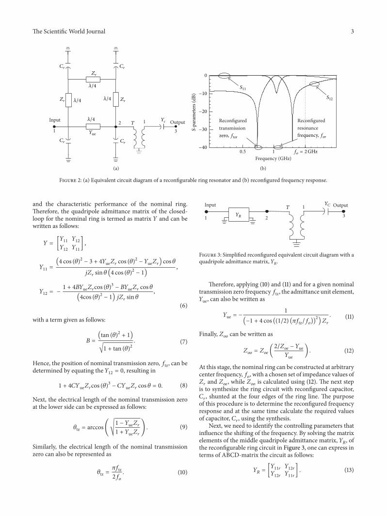
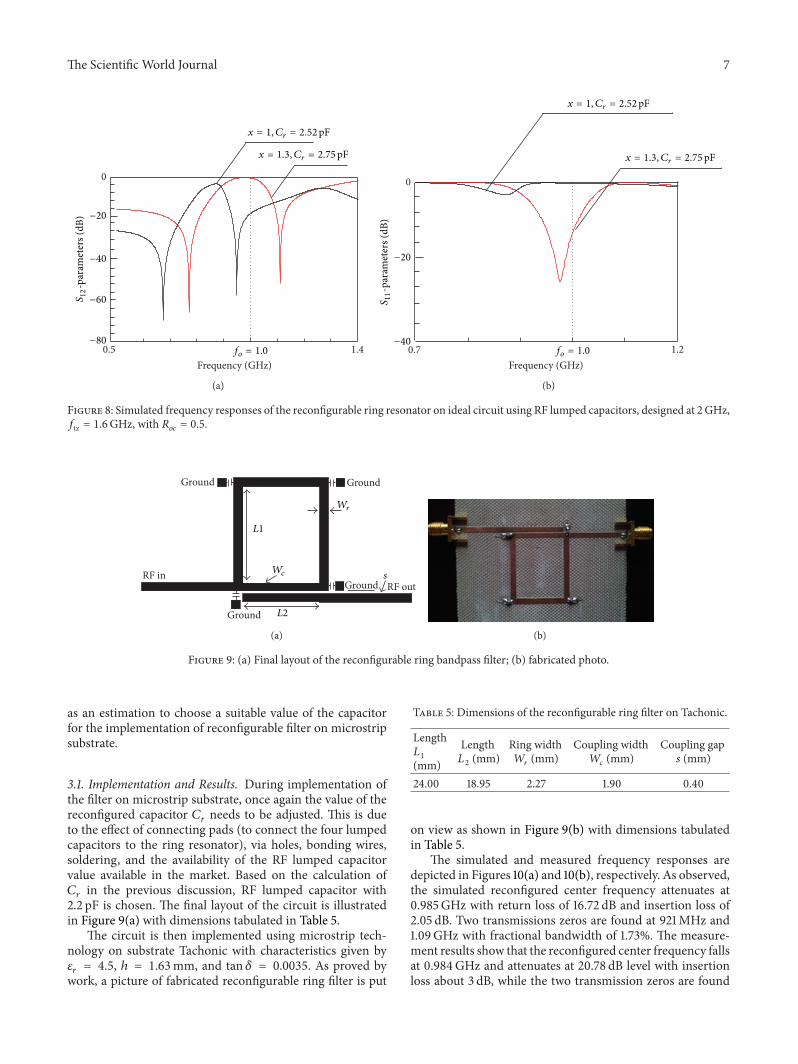
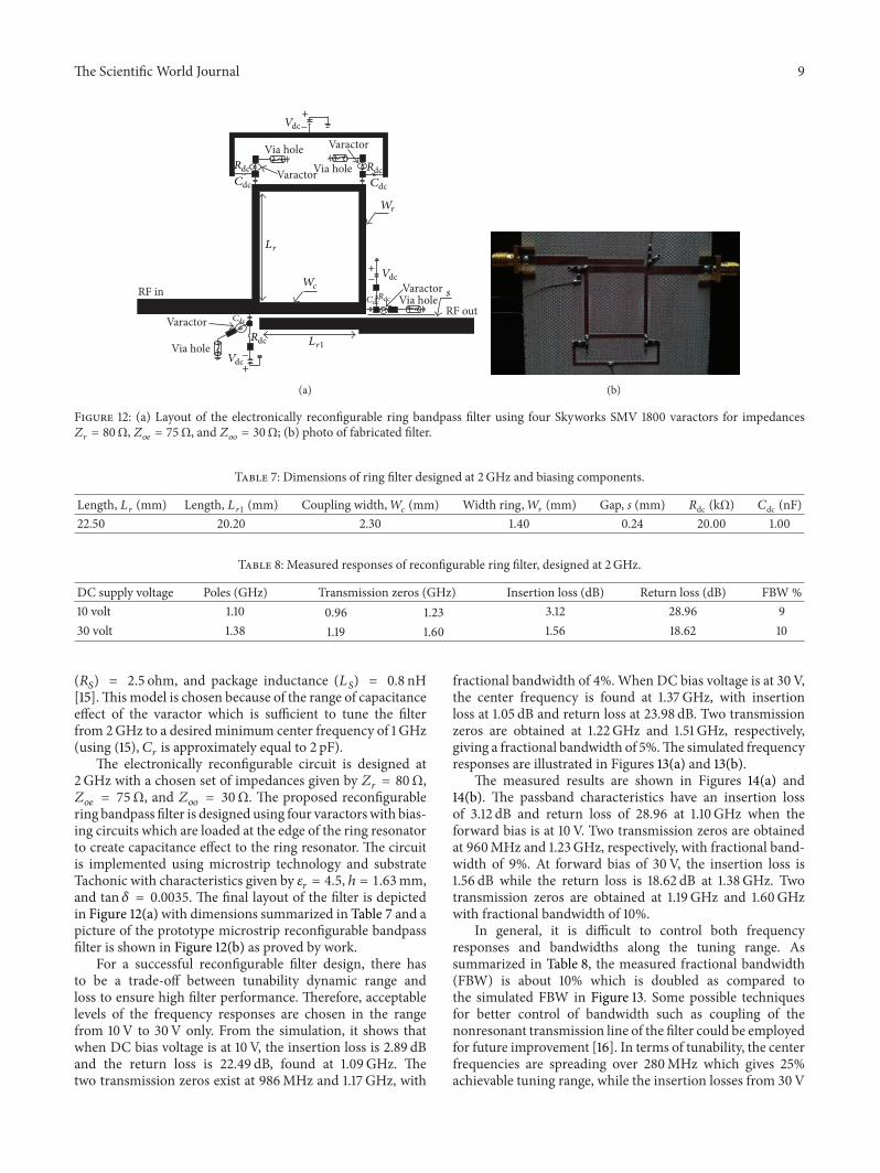

International Journal of
AerospaceEngineeringHindawi Publishing Corporationhttpwwwhindawicom Volume 2014
RoboticsJournal of
Hindawi Publishing Corporationhttpwwwhindawicom Volume 2014
Hindawi Publishing Corporationhttpwwwhindawicom Volume 2014
Active and Passive Electronic Components
Control Scienceand Engineering
Journal of
Hindawi Publishing Corporationhttpwwwhindawicom Volume 2014
International Journal of
RotatingMachinery
Hindawi Publishing Corporationhttpwwwhindawicom Volume 2014
Hindawi Publishing Corporation httpwwwhindawicom
Journal ofEngineeringVolume 2014
Submit your manuscripts athttpwwwhindawicom
VLSI Design
Hindawi Publishing Corporationhttpwwwhindawicom Volume 2014
Hindawi Publishing Corporationhttpwwwhindawicom Volume 2014
Shock and Vibration
Hindawi Publishing Corporationhttpwwwhindawicom Volume 2014
Civil EngineeringAdvances in
Acoustics and VibrationAdvances in
Hindawi Publishing Corporationhttpwwwhindawicom Volume 2014
Hindawi Publishing Corporationhttpwwwhindawicom Volume 2014
Electrical and Computer Engineering
Journal of
Advances inOptoElectronics
Hindawi Publishing Corporation httpwwwhindawicom
Volume 2014
The Scientific World JournalHindawi Publishing Corporation httpwwwhindawicom Volume 2014
SensorsJournal of
Hindawi Publishing Corporationhttpwwwhindawicom Volume 2014
Modelling amp Simulation in EngineeringHindawi Publishing Corporation httpwwwhindawicom Volume 2014
Hindawi Publishing Corporationhttpwwwhindawicom Volume 2014
Chemical EngineeringInternational Journal of Antennas and
Propagation
International Journal of
Hindawi Publishing Corporationhttpwwwhindawicom Volume 2014
Hindawi Publishing Corporationhttpwwwhindawicom Volume 2014
Navigation and Observation
International Journal of
Hindawi Publishing Corporationhttpwwwhindawicom Volume 2014
DistributedSensor Networks
International Journal of