resistance firing circuit€¦ · rc firing circuit by varying the variable resistance r v, the...
TRANSCRIPT

EE 6611- POWER ELECTRONICS & DRIVES LABORATORY
1 DEPT OF EEE-DMICE
CIRCUIT DIAGRAM: RESISTANCE FIRING CIRCUIT:
MODEL GRAPH

EE 6611- POWER ELECTRONICS & DRIVES LABORATORY
2 DEPT OF EEE-DMICE
Ex. No. 1 R, RC & UJT FIRING CIRCUIT FOR SCR
Date: AIM
To study operation of R, RC & UJT firing circuit for SCR
APPARATUS REQUIRED
S.No. APPARATUS RANGE TYPE QUA NTITY
1 SCR Module kit PEC16MIA 1
2 Patch Chords As required
3 Rheostat 220Ω/2A 1
THEORY RESISTANCE FIRING CIRCUIT
Resistance trigger circuits are the simplest & most economical method. During the
positive half cycle of the input voltage, SCR become forward biased but it will not conduct
until its gate current exceeds gate threshold, Vgt . Diode D allows the flow of current during
positive half cycle only. RV is the variable resistance and is used to limit the current through
the circuit (Ig) and to vary the gate voltage and thus the firing angle. During the positive half
cycle current Ig flows. Ig increases and when Vg=Vgt= IgminR the SCR turns ON .The firing angle
can be varied from 0 — 90° by varying the resistance R1.
RC FIRING CIRCUIT
By varying the variable resistance RV, the firing angle can be varied. Capacitor, C
charges and discharges with a phase shift. When the capacitor voltage equal to the gate
threshold voltage Vgt, SCR get triggered. Diode D prevents the negative voltage to gate.
UJT FIRING CIRCUIT
Diode Rectifier converts input ac to dc. Resistor R limits the circuit current to a
suitable value for the zener diode and UJT.Zener diode ‘Z’ functions to clip the rectified
voltage to a standard level. The zener voltage VZ is applied to the RC charging circuit.
Charging of capacitor C is at a rate determined by R1 and R3.When voltage across the
capacitor, V3 reaches the unijunction threshold voltage ηV2, the UJT junction breaks down
and the capacitor C discharges through the primary of pulse transformer. As the current is in
the form of pulse, windings of the pulse transformer have pulse voltages at their secondary
terminals and can turn on the SCR.As the charging rate of capacitor varies by varying R3,
firing angle can be controlled by varying R3.Firing angle can be controlled in a range of 0 0 to
1800.

EE 6611- POWER ELECTRONICS & DRIVES LABORATORY
3 DEPT OF EEE-DMICE
CIRCUIT DIAGRAM: RESISTANCE-CAPACITANCE FIRING CIRCUIT:
MODEL GRAPH

EE 6611- POWER ELECTRONICS & DRIVES LABORATORY
4 DEPT OF EEE-DMICE
R - FIRING CIRCUIT
Connection Procedure:
1. Connect the input supply to the module.
2. Connect P & N terminals to T7 & T9.
3. Connect one end of load rheostat to Anode of SCR.
4. Connect the other end of the load rheostat to the P terminal of 24V AC Supply.
5. Connect the cathode of SCR to the N terminal of 24V AC supply.
6. Connect G & K terminals of firing circuit to G & K terminals of SCR.
7. Connect the CRO ground to anode of SCR. Connect channel 1 probe to T7 & channel 2
probe to cathode of SCR.
Experiment Procedure:
1. Verify the connection as per the connection diagram.
2. Switch ON the 24V AC supply.
3. Observe the waveform for input AC voltage & Load voltage.
4. Calculate the DC output voltage using the equation
RC - FIRING CIRCUIT
Connection Procedure:
1. Connect the input supply to the module.
2. Connect P & N terminals to T12 & T13.
3. Connect one end of load rheostat to Anode of SCR.
4. Connect the other end of the load rheostat to the P terminal of 24V AC Supply.
5. Connect the cathode of SCR to the N terminal of 24V AC supply.
6. Connect G & K terminals of firing circuit to G & K terminals of SCR.
7. Connect the CRO ground to anode of SCR. Connect channel 1 probe to T12 & channel
2 probe to cathode of SCR.
Experiment Procedure:
1. Verify the connection as per the connection diagram.
2. Switch ON the 24V AC supply.
3. Observe the waveform for input AC voltage & Load voltage.
4. Calculate the DC output voltage using the equation

EE 6611- POWER ELECTRONICS & DRIVES LABORATORY
5 DEPT OF EEE-DMICE
CIRCUIT DIAGRAM: UJT FIRING CIRCUIT:
MODEL GRAPH

EE 6611- POWER ELECTRONICS & DRIVES LABORATORY
6 DEPT OF EEE-DMICE
R - FIRING CIRCUIT
Connection Procedure:
1. Connect the input supply to the module.
2. Connect one end of load rheostat to Anode of SCR.
3. Connect the other end of the load rheostat to the P terminal of 24V AC Supply.
4. Connect the cathode of SCR to the N terminal of 24V AC supply.
5. Connect G1 & K1 terminals of UJT firing circuit to G & K terminals of SCR.
Experiment Procedure:
1. Verify the connection as per the connection diagram.
2. Switch ON the 24V AC supply.
3. Connect the CRO ground to ground terminal of UJT firing circuit.
4. Observe the waveform for input AC voltage & Load voltage.
5. Calculate the DC output voltage using the equation
RESULT
Studied the operation of R, RC & UJT firing circuit for SCR .

EE 6611- POWER ELECTRONICS & DRIVES LABORATORY
7 DEPT OF EEE-DMICE
CIRCUIT DIAGRAM
MODEL GRAPH

EE 6611- POWER ELECTRONICS & DRIVES LABORATORY
8 DEPT OF EEE-DMICE
Ex. No. 2(a) CHARACTERISTICS OF SCR
Date: AIM
To determine the VI characteristics of SCR using PEC16MIA
APPARATUS REQUIRED
S.No. APPARATUS RANGE TYPE QUA NTITY
1 SCR Module kit PEC16MIA 1
2 Voltmeter (0-30) V MC 1
3 Ammeter (0-200)mA MC 2
4 Patch Chords As required
THEORY
An SCR is a unidirectional device as it can conduct from anode to cathode only.
SCR is a four layer, three junction, p-n-p-n semiconductor switching device. It has three
terminals anode, cathode & gate. The terminal connected to outer p region is called anode(A),
the terminal connected to outer n region is called cathode(K) & that connected to inner p
region is called gate (G). Static VI characteristics of a thyristor have three basic modes of
operation; namely, reverse blocking mode, forward blocking mode & forward conduction
mode.
PROCEDURE To determine the Characteristics of SCR
1) Make the connections as per the circuit diagram.
2) Switch on the supply
3) Set the gate current at a fixed value by varying POT on the gate-cathode side.
4) Now slowly increase the voltage (VAK) by varying the POT on the anode-cathode side
from zero until breakdown occurs.
5) Note down the breakdown voltage.
6) Further increase the anode to cathode voltage(VAK) & note down anode current (IA).
7) Draw the characteristics between anode to cathode voltage (VAK) and anode current
(IA).

EE 6611- POWER ELECTRONICS & DRIVES LABORATORY
9 DEPT OF EEE-DMICE
TABULAR COLUMN
S.No.
IG = (mA)
VAK (V) VAK (V)
IA (mA)

EE 6611- POWER ELECTRONICS & DRIVES LABORATORY
10 DEPT OF EEE-DMICE
RESULT
Thus the VI Characteristics of SCR using PEC16MIA was determined.

EE 6611- POWER ELECTRONICS & DRIVES LABORATORY
11 DEPT OF EEE-DMICE
CIRCUIT DIAGRAM
MODEL GRAPH

EE 6611- POWER ELECTRONICS & DRIVES LABORATORY
12 DEPT OF EEE-DMICE
Ex. No. 2(b) CHARACTERISTICS OF TRIAC
Date: AIM
To determine the VI characteristics of TRIAC using PEC16MIA
APPARATUS REQUIRED
S.No. APPARATUS RANGE TYPE QUA NTITY
1 TRIAC Module kit PEC16MIA 1
2 Voltmeter (0-30) V MC 1
3 Ammeter (0-200)mA MC 2
4 Patch Chords As required
THEORY
A TRIAC is a bidirectional device. It can conduct from anode to cathode & cathode
to anode. A TRIAC is equivalent to two SCRs connected in anti-parallel. It has three terminals
namely; main terminal1 (MT1), main terminal2 (MT2) & gate G. The terminal MT1 is the
reference point for measurement of voltages & currents at the gate terminal & at the terminal
MT2. The gate G is near to terminal MT1.
PROCEDURE To determine the Characteristics of TRIAC
1) Make the connections as per the circuit diagram.
2) Switch on the supply
3) Set the gate current at a fixed value by varying POT on the gate-MT1 side.
4) Now slowly increase the voltage (VMT1MT2) by varying the POT on the MT1-MT2 side
from zero until breakdown occurs.
5) Note down the breakdown voltage.
6) Further increase the MT1-MT2 voltage(VMT1MT2) & note down MT1 current (IMT!).
7) Draw the characteristics between MT1-MT2 voltage (VMT1MT2) and MT1 current
(IMT!).

EE 6611- POWER ELECTRONICS & DRIVES LABORATORY
13 DEPT OF EEE-DMICE
TABULAR COLUMN
IG = (mA)
S.No.
VMT1-MT2 (V) IMT1 (mA)

EE 6611- POWER ELECTRONICS & DRIVES LABORATORY
14 DEPT OF EEE-DMICE
RESULT
Thus the VI Characteristics of TRIAC using PEC16MIA was determined.

EE 6611- POWER ELECTRONICS & DRIVES LABORATORY
15 DEPT OF EEE-DMICE
CIRCUIT DIAGRAM MODEL GRAPH
EE 6611- POWER ELECTRONICS & DRIVES LABORATORY
16 DEPT OF EEE-DMICE
Ex. No. 3(A) CHARACTERISTICS OF MOSFET
Date: AIM
To determine the output & transfer characteristics of MOSFET using PEC16MIA
APPARATUS REQUIRED
S.No. APPARATUS RANGE TYPE QUA NTITY
1 MOSFET Module kit PEC16MIA 1
2 Voltmeter (0-30) V MC 2
3 Ammeter (0-200)mA MC 2
4 Patch Chords As required
THEORY
A metal oxide semiconductor field effect transistor(MOSFET) is a voltage
controlled device. As its operation depends upon the flow of majority carriers only, MOSFET
is a unipolar device. A power MOSFET has three terminals called drain(D),source(S) &
Gate(G). In symbol of MOSFET arrow indicates the direction of electrons flow. The static
characteristics of MOSFET are output & transfer characteristics. MOSFETs are widely used
for high frequency applications.
PROCEDURE To determine the Output Characteristics of MOSFET
1) Make the connections as per the circuit diagram.
2) Switch on the supply
3) Set the gate-source voltage (VGS) at a fixed value by varying POT on the gate side.
4) Now slowly increase the drain-source voltage (VDS) by varying the POT on drain-
source side from zero till the MOSFET gets turn ON.
5) Note down the VDS& ID.
6) Further increase the drain-source voltage (VDS) & note down ID.
7) Draw the characteristics between drain-source voltage (VDS)and drain current ID.

EE 6611- POWER ELECTRONICS & DRIVES LABORATORY
17 DEPT OF EEE-DMICE
OUTPUT CHARACTERISTICS
VGS = (V) S.No
VDS (V) ID (mA) TRANSFER CHARACTERISTICS
S.No V DS = (V)
VGS (V) ID (mA)

EE 6611- POWER ELECTRONICS & DRIVES LABORATORY
18 DEPT OF EEE-DMICE
To determine the transfer Characteristics of MOSFET
1) Make the connections as per the circuit diagram.
2) Switch on the supply
3) Set the drain-source voltage (VDS) at a fixed value by varying POT on the drain-
source side.
4) Now slowly increase the gate-source voltage (VGS) by varying the POT on gate side
from zero till the MOSFET gets turn ON.
5) Note down the VGS& ID.
6) Further increase the gate-source voltage (VGS) & note down ID.
7) Draw the characteristics between gate-source voltage (VGS)and drain current ID.
RESULT
Thus the output & transfer characteristics of MOSFET using PEC16MIA
were determined.

EE 6611- POWER ELECTRONICS & DRIVES LABORATORY
19 DEPT OF EEE-DMICE
CIRCUIT DIAGRAM
MODEL GRAPH
EE 6611- POWER ELECTRONICS & DRIVES LABORATORY
20 DEPT OF EEE-DMICE
Ex. No. 3(B) CHARACTERISTICS OF IGBT
Date: AIM
To determine the output & transfer characteristics of IGBT using PEC16MIA
APPARATUS REQUIRED
S.No. APPARATUS RANGE TYPE QUA NTITY
1 IGBT Module kit PEC16MIA 1
2 Voltmeter (0-30) V MC 2
3 Ammeter (0-200)mA MC 2
4 Patch Chords As required
THEORY
Insulated Gate Bipolar Transistor (IGBT), combines the advantages of both BJT &
MOSFET. So an IGBT has high input impedance like MOSFET & low on state power loss as in a
BJT. IGBT is free from second breakdown problem. A IGBT has three terminals called
collector(C), emitter (E) & Gate(G). The static characteristics of IGBT are output & transfer
characteristics. IGBTs are used in medium power applications such as dc & ac drives.
PROCEDURE To determine the Output Characteristics of IGBT
1) Make the connections as per the circuit diagram.
2) Switch on the supply
3) Set the gate-emitter voltage (VGE) at a fixed value by varying POT on the gate side.
4) Now slowly increase the collector-emitter voltage (VCE) by varying the POT on
collector-emitter side from zero till the IGBT gets turn ON.
5) Note down the VCE& IC.
6) Further increase the collector-emitter voltage (VCE) & note down IC.
7) Draw the characteristics between collector-emitter voltage (VCE) and collector current IC.

EE 6611- POWER ELECTRONICS & DRIVES LABORATORY
21 DEPT OF EEE-DMICE
OUTPUT CHARACTERISTICS
VGE = (V) S.No
VCE (V) IC (mA) TRANSFER CHARACTERISTICS
S.No VCE = (V)
VGE (V) IC (mA)

EE 6611- POWER ELECTRONICS & DRIVES LABORATORY
22 DEPT OF EEE-DMICE
To determine the transfer Characteristics of IGBT
1) Make the connections as per the circuit diagram.
2) Switch on the supply
3) Set the collector-emitter voltage (VCE) at a fixed value by varying POT on the
collector-emitter side.
4) Now slowly increase the gate-emitter voltage (VGE) by varying the POT on gate
side from zero till the IGBT gets turn ON.
5) Note down the VGE& IC.
6) Further increase the gate-emitter voltage (VGE) & note down IC.
7) Draw the characteristics between gate-emitter voltage (VGE) and collector current IC.
RESULT
Thus the output & transfer characteristics of IGBT using PEC16MIA were determined.

EE 6611- POWER ELECTRONICS & DRIVES LABORATORY
23 DEPT OF EEE-DMICE
CIRCUIT DIAGRAM
MODEL GRAPH

EE 6611- POWER ELECTRONICS & DRIVES LABORATORY
24 DEPT OF EEE-DMICE
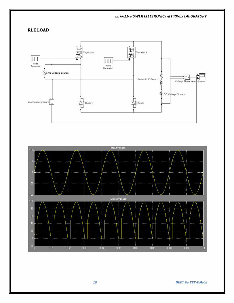
Ex. No. 4 AC TO DC HALF CONTROLLED CONVERTER
Date: AIM
To construct a single phase half controlled Converter and plot its output response.
APPARATUS REQUIRED
S.NO. APPARATUS RANGE TYPE QUANTITY
1 Half controlled Converter
1, 230V,10A - 1
Power circuit kit
2 SCR firing circuit kit 1 ,230V,5A - 1
3 CRO 20MHz - 1
4 Patch chords - - As Required
THEORY
A rectifier is a device which converts input ac signal into output dc signal. A
thyristor is turned off as ac supply voltage reverse biases it, provided anode current has
fallen to a level below the holding current. A single phase semi converter topology employs
two SCRs & two diodes. It employs one SCR & one diode in each leg. It offers one-quadrant
operation. Freewheeling action in semi-converter circuits render better power factor.
FORMULA
PROCEDURE
1. Make the connections as per the circuit diagram.
2. Switch on the thyristor kit and firing circuit kit.
3. Vary the firing angle in steps.
4. Observe the waveform from the CRO & Note down the Input & Output, Amplitude &
time readings.
5. Draw the Output Response.

EE 6611- POWER ELECTRONICS & DRIVES LABORATORY
25 DEPT OF EEE-DMICE
TABULATOR COLUMN
S.No. Amplitude(V)
Time Period Firing Angle Output Voltage
(mS) (D egree) Vo (Volts)

EE 6611- POWER ELECTRONICS & DRIVES LABORATORY
26 DEPT OF EEE-DMICE
SIMULATION
R LOAD

EE 6611- POWER ELECTRONICS & DRIVES LABORATORY
27 DEPT OF EEE-DMICE
RL LOAD
EE 6611- POWER ELECTRONICS & DRIVES LABORATORY
28 DEPT OF EEE-DMICE
RLE LOAD

EE 6611- POWER ELECTRONICS & DRIVES LABORATORY
29 DEPT OF EEE-DMICE

EE 6611- POWER ELECTRONICS & DRIVES LABORATORY
30 DEPT OF EEE-DMICE
RESULT
Thus a single-phase half controlled converter was constructed and their Output
waveforms were plotted.

EE 6611- POWER ELECTRONICS & DRIVES LABORATORY
31 DEPT OF EEE-DMICE
CIRCUIT DIAGRAM
MODEL GRAPH

EE 6611- POWER ELECTRONICS & DRIVES LABORATORY
32 DEPT OF EEE-DMICE
Ex. No. 5 AC TO DC FULLY CONTROLLED CONVERTER
Date: AIM
To construct a single phase fully controlled Converter and plot its response.
APPARATUS REQUIRED
S.NO ITEM RANGE QUA NTITY
1 Fully controlled Converter Power 1, 230V,10A 1 circuit kit
2 SCR firing circuit kit 1 ,230V,5A 1
3 CRO 20MHz 1
4 Patch chords - As Required
THEORY
A single phase full converter employs four SCRs.. When an incoming SCR is turned
on by triggering, it immediately reverse biases the outgoing SCR & turns it off. It can furnish
two-quadrant operation. A firing angle is defined as the angle measured from the instant
that gives the largest average output voltage to the instant it is triggered. Phase Control is
used for controlling the load currents.
FORMULA
PROCEDURE:
1. Make the connections as per the circuit diagram.
2. Switch on the thyristor kit and firing circuit kit.
3. Vary the firing angle in steps.
4. Observe the waveform from the CRO & Note down the Input & Output, Amplitude &
time readings.
5. Draw the Output Response.

EE 6611- POWER ELECTRONICS & DRIVES LABORATORY
33 DEPT OF EEE-DMICE
TABULATOR COLUMN
S.No. Amplitude(V)
Time Period Firing Angle Output Voltage
(mS) (D egree) Vo (Volts)

EE 6611- POWER ELECTRONICS & DRIVES LABORATORY
34 DEPT OF EEE-DMICE
SIMULATION
a) 1 Ф FULL CONVERTER
R LOAD

EE 6611- POWER ELECTRONICS & DRIVES LABORATORY
35 DEPT OF EEE-DMICE
RL LOAD

EE 6611- POWER ELECTRONICS & DRIVES LABORATORY
36 DEPT OF EEE-DMICE
RLE LOAD

EE 6611- POWER ELECTRONICS & DRIVES LABORATORY
37 DEPT OF EEE-DMICE
b) 3 Ф FULL CONVERTER
R LOAD
α = 00

EE 6611- POWER ELECTRONICS & DRIVES LABORATORY
38 DEPT OF EEE-DMICE
α = 300
RESULT Thus a single-phase fully controlled converter was constructed and their responses were
plotted.

EE 6611- POWER ELECTRONICS & DRIVES LABORATORY
39 DEPT OF EEE-DMICE
CIRCUIT DIAGRAM
STEP DOWN CHOPPER
STEP UP CHOPPER

EE 6611- POWER ELECTRONICS & DRIVES LABORATORY
40 DEPT OF EEE-DMICE
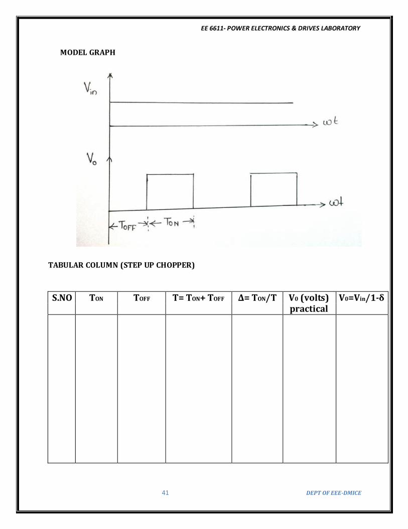
Ex. No. 6 STEP UP AND STEP DOWN MOSFET BASED CHOPPERS
Date:
AIM
To construct Step down & Step up MOSFET based chopper and to draw its output
response.
APPARATUS REQUIRED
S.NO ITEM RANGE QUA NTITY
1 Step up & Step down MOSFET 1
based chopper kit
2 RPS 1
3 Rheostat 1
4 CRO 20 MHZ 1
5 Patch chords As required
THEORY
A chopper is a static device that converts fixed dc input voltage to a variable dc
output voltage directly.
Average output voltage Vo is less than the input voltage Vs , Vo<Vs; This
configuration is therefore called step down chopper. Average output voltage V o greater
than input voltage Vs, Vo>Vs; This configuration is therefore called step up chopper.
FORMULA:
STEP DOWN CHOPPER:
V0=Vinδ
STEP UP CHOPPER:
V0=Vin/1-δ
Where, V0–Output Voltage
Vin-Input Voltage
δ – Duty Cycle
EE 6611- POWER ELECTRONICS & DRIVES LABORATORY
41 DEPT OF EEE-DMICE
MODEL GRAPH
TABULAR COLUMN (STEP UP CHOPPER)
S.NO TON TOFF T= TON+ TOFF Δ= TON/T V0 (volts) V0=Vin/1-δ
practical

EE 6611- POWER ELECTRONICS & DRIVES LABORATORY
42 DEPT OF EEE-DMICE
PROCEDURE (STEP UP CHOPPER & STEP DOWN CHOPPER)
1. Make the connection as per the circuit diagram
2. Initially keep all the switches in the OFF position
3. Initially keep duty cycle POT in minimum position
4. Connect DC supply from variable DC source
5. Set the input DC supply to 10V. View the input voltage in CRO.
6. Then switch ON the driver circuit & power circuit
7. Observe the output voltage across the load
8. Draw the waveform for different duty cycle & different frequency.

EE 6611- POWER ELECTRONICS & DRIVES LABORATORY
43 DEPT OF EEE-DMICE
TABULAR COLUMN (STEP DOWN CHOPPER)
S.NO TON TOFF T= TON+ TOFF Δ= TON/T V0 (volts) V0=Vinδ
practical

EE 6611- POWER ELECTRONICS & DRIVES LABORATORY
44 DEPT OF EEE-DMICE
SIMULATION
a) STEP DOWN CHOPPER

EE 6611- POWER ELECTRONICS & DRIVES LABORATORY
45 DEPT OF EEE-DMICE
a) STEP UP CHOPPER

EE 6611- POWER ELECTRONICS & DRIVES LABORATORY
46 DEPT OF EEE-DMICE
RESULT
Thus the operation of a step up & step down MOSFET based chopper was determined.

EE 6611- POWER ELECTRONICS & DRIVES LABORATORY
47 DEPT OF EEE-DMICE
CIRCUIT DIAGRAM
MODEL GRAPH

EE 6611- POWER ELECTRONICS & DRIVES LABORATORY
48 DEPT OF EEE-DMICE
Ex. No. 7 IGBT BASED SINGLE PHASE PWM INVERTER
Date: AIM
To obtain Single phase output wave forms for IGBT based PWM inverter.
APPARATUS REQUIRED
S.No. ITEM RANGE TYPE QUA NTITY
1 IGBT Based PWM inverter Kit 220/10A 1
2 Inverter Control Module PEC16MIA 1
3 CRO 20MHZ 1
4 Load rheostat 50/5A 1
5 Patch Chord As required
THEORY
PWM inverters are characterized by constant amplitude pulses. The width of these
pulses is modulated to obtain inverter output voltage control & to reduce its harmonic
content.
A fixed dc input voltage is given to inverter & a controlled ac output voltage is
obtained by adjusting on & off periods of the inverter components. Pulse Width
Modulation is the most popular method of controlling the output voltages.
FORMULA
Modulation Index, M=Ar/Ac or Vr/Vc
Output Voltage, Vo=Vin*M
PROCEDURE
1. Make the connection as per the circuit diagram.
2. Connect the gating signal from the inverter module.
3. Switch ON D.C 24 V.
4. Keep the frequency knob to particulars frequency.
5. Observe the rectangular and triangular carrier waveforms on the CRO.
6. Obtain the output waveform across the load Rheostat.

EE 6611- POWER ELECTRONICS & DRIVES LABORATORY
49 DEPT OF EEE-DMICE
TABULAR COLUMN
Vin Vref Vcarrier M= Output
Vr/Vc
Amplitude Time Amplitude Time Vo Vo
(Practical)
(Theoretical)

EE 6611- POWER ELECTRONICS & DRIVES LABORATORY
50 DEPT OF EEE-DMICE
SIMULATION
RESULT
Thus the operation of a IGBT based Single phase PWM modulation was determined.

EE 6611- POWER ELECTRONICS & DRIVES LABORATORY
51 DEPT OF EEE-DMICE
CIRCUIT DIAGRAM
MODEL GRAPH

EE 6611- POWER ELECTRONICS & DRIVES LABORATORY
52 DEPT OF EEE-DMICE
Ex. No. 8 IGBT BASED THREE PHASE PWM INVERTER
Date: AIM
To operate forward & reverse mode three phase induction motor using IGBT based
on three phase PWM inverter.
APPARATUS REQUIRED
S.No. ITEM RANGE TYPE QUANTITY
1 IGBT Based PWM inverter Kit 230V 3ɸ 1
2 Three Phase Induction Motor 230V 3ɸ 1
3 Tachometer 1
4 Patch Chord As required
THEORY
A device that converts dc power into ac power at desired output voltage &
frequency is called an inverter. For providing adjustable frequency power to industrial
applications, three phase inverters are more common than single phase inverters.
A three phase inverter is a six step bridge inverter. It uses a minimum of six
thyristors. A step is defined as a change in the firing from one thyristor to the next thyristor
in proper sequence.
PROCEDURE
1. Make the connection as per the circuit diagram.
2. Switch ON the supply
3. Select the forward rotation mode
4. By varying the frequency for regulated interval, note down the speed of IM
using tachometer.
5. Then select the reverse rotation mode
6. By varying the frequency for regulated interval, note down the speed of IM
using tachometer.
7. The graph is plotted for forward mode & reverse mode.

EE 6611- POWER ELECTRONICS & DRIVES LABORATORY
53 DEPT OF EEE-DMICE
TABULAR C OLUM N (FORWARD M ODE)
S.No. Speed (N) Frequency(Hz)
TABULAR COLUMN (REVERSE MODE)
S.No. Speed (N) Frequency(Hz)

EE 6611- POWER ELECTRONICS & DRIVES LABORATORY
54 DEPT OF EEE-DMICE
SIMULATION
a) THREE PHASE INVERTER-180

EE 6611- POWER ELECTRONICS & DRIVES LABORATORY
55 DEPT OF EEE-DMICE

EE 6611- POWER ELECTRONICS & DRIVES LABORATORY
56 DEPT OF EEE-DMICE
b) THREE PHASE INVERTER-120
RESULT
Thus the forward & reverse mode of three phase Induction motor using IGBT
based PWM inverter was obtained.

EE 6611- POWER ELECTRONICS & DRIVES LABORATORY
57 DEPT OF EEE-DMICE
CIRCUIT DIAGRAM AC Phase Control using SCR
AC Phase Control using TRIAC & DIAC

EE 6611- POWER ELECTRONICS & DRIVES LABORATORY
58 DEPT OF EEE-DMICE
Ex. No. 9 AC Phase Control using SCR, TRIAC & DIAC
Date: AIM
To control the output voltage by AC phase control using SCR, TRIAC & DIAC.
APPARATUS REQUIRED
S.No. ITEM RANGE TYPE QUANTITY
1 Trainer Kit PEC14M22 1
2 Voltmeter 0-230V MC 1
3 CRO & Lamp 1
4 Patch Chord As required
THEORY
AC Phase control using SCR
Two SCRs connected in antiparallel. T1 & T2 are forward biased during positive &
negative half cycles respectively. During first half cycle , T1 is triggered at firing angle α.T1
starts conducting and source voltage is applied to load from α to β. At both V 0& Io are all to
zero. Just afterse T1 is subjected to reverse biased and is therefore turned OFF. During
negative half cycle, T2 is triggered at α+β. T2 conducts from (α+π) to 2π. Soon after 2π, T2
is subjected to reverse biased and is therefore commutated.
AC Phase control using TRIAC & DIAC
Triac is a bidirectional thyristor with three terminals. Triac is the word derived by
combining the capital letters from the words TRIode and AC. In operation triac is equivalent to
two SCRs connected in anti-parallel. It is used extensively for the control of power in ac circuit
as it can conduct in both the direction. Its three terminals are MT1 (main terminal 1), MT2 (main
terminal 2) and G (gate).

EE 6611- POWER ELECTRONICS & DRIVES LABORATORY
59 DEPT OF EEE-DMICE
MODEL GRAPH

EE 6611- POWER ELECTRONICS & DRIVES LABORATORY
60 DEPT OF EEE-DMICE
AC Phase control using SCR
CONNECTION PROCEDURE
1. Connect P3 TO P5 & P4 to P6.
2. Connect cathode and gate of SCR 1 & 2(G1, K1 & G2, K2) to pulse 1 and pulse 2
respectively.
3. Connect the P23 to P24, P1 to P15, P2 TO P16, P19 to P17 & P20 to P18.
4. Connect the input with 230 V power supply and the output with the load.
5. Insert a lamp in the lamp holder.
6. Connect the voltmeter across the load.
EXPERIMETAL PROCCEDURE
1. Switch ON the power supply by switching ON S1.
2. View test signals on the CRO.
3. By varying the firing angles and note down the corresponding readings of voltmeter.
4. Variation of voltage can be indicated by the dimness and brightness of the lamp.
AC Phase control using TRIAC & DIAC
CONNECTION PROCEDURE
1. Connect the P23 to P24, P1 to P21, P2 TO P22, P19 to P26&P20 to P25.
2. Connect the input with 230 V power supply and the output with the load.
3. Insert a lamp in the lamp holder.
4. Connect the voltmeter across the load.
EXPERIMETAL PROCCEDURE
1. Switch ON the power supply.
2. View test signals on the CRO.
3. By varying the firing angles and note down the corresponding readings of voltmeter.
4. Variation of voltage can be indicated by the dimness and brightness of the lamp.

EE 6611- POWER ELECTRONICS & DRIVES LABORATORY
61 DEPT OF EEE-DMICE
TABULAR COLUMN
AC PHASE CONTROL USING SCR
S.no Firing angle (α) Output voltage (volts)
AC PHASE CONTROL USING TRIAC & DIAC
S.no Firing angle (α) Output voltage (volts)

EE 6611- POWER ELECTRONICS & DRIVES LABORATORY
62 DEPT OF EEE-DMICE
SIMULATION
RESULT
Thus the output can be controlled by AC phase control using SCR, TRIAC DIAC & the
waveforms will be plotted.

EE 6611- POWER ELECTRONICS & DRIVES LABORATORY
63 DEPT OF EEE-DMICE
CIRCUIT DIAGRAM BUCK CONVERTER
MODEL GRAPH
MOSFET
D S
G Vin
Dm
Vout C
L

EE 6611- POWER ELECTRONICS & DRIVES LABORATORY
64 DEPT OF EEE-DMICE
Ex. No. 10 SWITCHED MODE POWER CONVERTERS
Date:
AIM To design and draw the input and output waveform for Buck & Boost Converter.
APPARATUS REQUIRED
S.No. ITEM RANGE TYPE QUANTITY
1 SMPS Kit 1
2 CRO 1
3 Patch Chord As required
THEORY
BUCK CONVERTER
A buck converter is a voltage step down and current step up converter. With the
switch open (off-state), the current in the circuit is zero. When the switch is first closed
(on-state), the current will begin to increase. Over time, the rate of change of current
decreases, and the voltage across the inductor also then decreases, increasing the voltage at
the load. During this time, the inductor stores energy in the form of a magnetic field. If the
switch is opened while the current is still changing, then there will always be a voltage drop
across the inductor, so the net voltage at the load will always be less than the input voltage
source.
BOOST CONVERTER
A boost converter (step-up converter) is a DC-to-DC power converter with an
output voltage greater than its input voltage.
(a) When the switch is closed, electrons flow through the inductor in clockwise direction
and the inductor stores some energy by generating a magnetic field. Polarity of the left side
of the inductor is positive.
(b) When the switch is opened, current will be reduced as the impedance is higher. The
magnetic field previously created will be destroyed to maintain the current towards the
load. Thus the polarity will be reversed. As a result two sources will be in series causing a
higher voltage to charge the capacitor through the diode D.

EE 6611- POWER ELECTRONICS & DRIVES LABORATORY
65 DEPT OF EEE-DMICE
CIRCUIT DIAGRAM BOOST CONVERTER
MODEL GRAPH
MOSFET
D
S
G Vin
Dm
Vout
C
L

EE 6611- POWER ELECTRONICS & DRIVES LABORATORY
66 DEPT OF EEE-DMICE
PROCEDURE
1. Give the triggering circuit connections as per the patching diagram.
2. Switch ON the main supply.
3. Connect the CRO to the output terminals to study the waveform.
4. Set the carrier wave frequency between 5 KHz to 10 KHz using frequency knob.
5. Vary the duty cycle and observe the output.

EE 6611- POWER ELECTRONICS & DRIVES LABORATORY
67 DEPT OF EEE-DMICE
TABULAR COLUMN:
Buck Converter
S.No Vin TON TOFF δ = TON/ T Vo = δVs
Theoritical Practical
Boost Converter
S.No Vin TON TOFF δ = TON/ T Vo = δ Vs
Theoritical Practical

EE 6611- POWER ELECTRONICS & DRIVES LABORATORY
68 DEPT OF EEE-DMICE
Result
Thus the design and Input/output waveforms for Buck & Boost converter are
drawn.