section 1: hardcopy ii device family data sheet
TRANSCRIPT

Altera Corporation Section I–1Preliminary
Section I. HardCopy IIDevice Family Data Sheet
This section provides designers with the data sheet specifications for HardCopy® II devices. These chapters contain feature definitions of the internal architecture, configuration and JTAG boundary-scan testing information, DC operating conditions, AC timing parameters, a reference to power consumption, and ordering information for HardCopy II devices.
This section contains the following:
■ Chapter 1, Introduction to HardCopy II Devices
■ Chapter 2, Description, Architecture, and Features
■ Chapter 3, Boundary-Scan Support
■ Chapter 4, DC and Switching Specifications and Operating Conditions
■ Chapter 5, Quartus II Support for HardCopy II Devices
■ Chapter 6, Script-Based Design for HardCopy II Devices
■ Chapter 7, Timing Constraints for HardCopy II Devices
■ Chapter 8, Migrating Stratix II Device Resources to HardCopy II Devices
Revision History Refer to each chapter for its own specific revision history. For information on when each chapter was updated, refer to the Chapter Revision Dates section, which appears in the complete handbook.
Section I–2 Altera CorporationPreliminary
Revision History HardCopy Series Handbook, Volume 1
Altera Corporation 1–1June 2007 Preliminary
1. Introduction to HardCopy IIDevices
Introduction HardCopy® II devices are low-cost, high-performance structured ASICs with pin-outs, densities, and architecture that complement Stratix® II devices. HardCopy II device features, such as phase-locked loops (PLLs), memory, and I/O elements (IOEs), are functionally and electrically equivalent to the Stratix II FPGA features. The combination of Stratix II FPGAs for in-system prototype and design verification, HardCopy II devices for high-volume production, and the Quartus® II software for design, provide a complete, low-risk design solution.
HardCopy II devices improve on the successful and proven methodology of the two previous generations of HardCopy series devices. Altera® HardCopy II devices use the same base arrays across multiple designs for a given device density and are customized using only two metal layers. HardCopy II devices offer up to 90% cost reduction compared to Stratix II FPGA prototypes.
The Quartus II software provides a complete set of tools, common for both designing Stratix II FPGA prototypes and for quickly migrating the design to a HardCopy II companion device. HardCopy II devices are also supported through other front-end design tools from Synopsys, Synplicity, and Mentor Graphics®.
Feature Overview
HardCopy II structured ASICs are manufactured on a 1.2 V, 90 nm all-layer-copper metal fabrication process (up to nine layers of metal). HardCopy II devices offer the following features:
■ Fine-grained HCell architecture resulting in a low-cost, high-performance, low-power structured ASIC
■ Customized using only two metal layers for fast turn-around times and low non-recurring expenses (NRE)
■ Fully tested prototypes are available in approximately 10 to 12 weeks from the date of your design submission
■ Support for instant-on or instant-on-after-50-ms power-up modes■ Preserves the design functionality of a Stratix II FPGA prototype■ 1,000,000 to 3,600,000 usable gates for both logic and DSP functions
H51015-2.5
1–2 Altera CorporationPreliminary June 2007
HardCopy Series Handbook, Volume 1
■ System performance up to 350 MHz■ Up to 50% power reduction (dynamic and static) for typical designs
compared to Stratix II FPGA prototypes
1 The actual performance and power consumption improvements mentioned in this datasheet are design-dependent.
■ Internal Memory● Up to 8,847,360 RAM bits available (including parity bits)● True dual-port memory, suitable for use in first-in-first-out
(FIFO) buffers■ Phase-Locked Loops (PLLs)
● Up to 16 global clocks with 24 clocking resources per device region
● Clock control block supports dynamic clock network enable/disable and dynamic global clock network source selection
● Up to 12 PLLs (four enhanced PLLs and eight fast PLLs) per device which provide identical features as the FPGA counterparts, including spread spectrum, programmable bandwidth, clock switchover, real-time PLL reconfiguration, advanced multiplication, and phase shifting
■ I/O Standards and Intellectual Property (IP)● Support for numerous single-ended and differential I/O
standards such as LVTTL, LVCMOS, PCI, PCI-X, SSTL, HSTL, and LVDS
● High-speed differential I/O support on up to 116 channels with dynamic phase alignment (DPA) circuitry for 1-Gigabit-per-second (Gbps) performance
● Support for high-speed networking and communications bus standards including Parallel RapidIO, SPI-4 Phase 2 (POS-PHY Level 4), HyperTransport™ technology, and SFI-4
● Support for high-speed external memory, including DDR and DDR2 SDRAM, RLDRAM II, QDRII SRAM, and SDR SDRAM
● Support for multiple intellectual property megafunctions from Altera MegaCore® functions, and Altera Megafunction Partners Program (AMPPSM) megafunctions
■ Packaging● Pin-compatible with Stratix II FPGA prototypes● Up to 951 user I/O pins available● Available in wire bond and flip-chip space-saving
FineLine BGA packages (Table 1–3).

Altera Corporation 1–3June 2007 Preliminary
Feature Overview
The HardCopy II device family consists of five devices. Table 1–1 summarizes the features available in the HardCopy II devices.
Table 1–1. HardCopy II Device Family Features
Feature HC210W (1) HC210 HC220 HC230 HC240
ASIC equivalent gates (2) 1,000,000 1,000,000 1,900,000 2,900,000 3,600,000
M4K RAM blocks(4 Kbits plus parity)
190 190 408 614 768 (3)
M-RAM blocks (512 Kbits plus parity)
0 0 2 6 9
Total RAM bits (including parity bits)
875,520 875,520 3,059,712 6,368,256 8,847,360
Enhanced PLLs 2 2 2 4 4
Fast PLLs 2 2 2 4 8
Maximum user I/O pins (4), (5) 308 334 494 698 951
Notes to Table 1–1:(1) HC210W devices are in a wire bond package. All other HardCopy II devices and Stratix II FPGAs use a flip-chip
package. Devices in a wire bond package offer different performance and signal integrity characteristics compared to devices in a flip-chip package.
(2) This is the number of ASIC equivalent gates available in the HardCopy II base array, shared between both adaptive logic module (ALM) logic and DSP functions from a Stratix II FPGA prototype. Each Stratix II adaptive logic module (ALM) is equal to approximately 30 ASIC equivalent gates. The number of ASIC equivalent gates usable is bounded by the number of ALMs in the companion Stratix II FPGA device.
(3) Total number of usable M4K blocks is 768, which allows migration compatibility when prototyping with an EP2S180 device. This may be different from the Quartus II software total physical M4K count of the HC240.
(4) The I/O pin counts include the dedicated CLK input pins, which can be used for clock signals or data inputs.(5) The Quartus II I/O pin counts include an additional pin (PLLENA), which is not available as a general-purpose I/O
pin. The PLLENA pin can only be used to enable the PLLs.

1–4 Altera CorporationPreliminary June 2007
HardCopy Series Handbook, Volume 1
Migration and Packaging Overview
HardCopy II devices offer pin-to-pin compatibility to the Stratix II prototype, which makes them drop-in replacements for the FPGAs. Therefore, the same system board and software developed for prototyping and field trials can be retained, enabling the fastest time-to-market for high-volume production. When migrating a specific Stratix II FPGA to a HardCopy II device, there are a number of FPGA prototype choices, as shown in Table 1–2. Depending on the design resource needs, designers can choose an appropriate HardCopy II device.
Table 1–2. Stratix II FPGA to HardCopy II Migration Paths
HardCopy II Device Package
Stratix II Device
EP2S30 EP2S60 EP2S90 EP2S130 EP2S180
HC210W 484-pin FineLine BGA (1) v v v (2)
HC210 484-pin FineLine BGA v v v (2)
HC220 672-pin FineLine BGA v
HC220 780-pin FineLine BGA v v (2)
HC230 1,020-pin FineLine BGA v v v (2)
HC240 1,020-pin FineLine BGA v
HC240 1,508-pin FineLine BGA v
Notes to Table 1–2:(1) The HC210W device uses a wire bond package while the Stratix II FPGA prototype device uses a pin-compatible
flip-chip package. (2) Depending on design specific resource utilization, an opportunistic migration path may exist between this device
pair. Be sure to confirm your design is a potential candidate for such a path by fitting with the Quartus II software and consulting an Altera applications engineer.

Altera Corporation 1–5June 2007 Preliminary
Document Revision History
HardCopy II devices are available in the packages shown in Table 1–3.
Document Revision History
Table 1–4 shows the revision history for this chapter.
Table 1–3. HardCopy II Package Options and I/O Pin Counts Notes (1), (2)
Package484-Pin
FineLine BGA (3)
484-Pin FineLine BGA
(3)
672-Pin FineLine BGA
780-Pin FineLine BGA
1,020-Pin FineLine BGA
1,508-Pin FineLine BGA
Type Wire bond Flip-chip Flip-chip Flip-chip Flip-chip Flip-chip
Dimension
Pitch (mm) 1.00 1.00 1.00 1.00 1.00 1.00
Area (mm2) 529 529 729 841 1,089 1,600
Length × width (mm × mm)
23 × 23 23 × 23 27 × 27 29 × 29 33 × 33 40 × 40
Device Maximum User I/O Pins
HC210W 308
HC210 334
HC220 492 494
HC230 698
HC240 742 951
Notes to Table 1–3:(1) The Quartus II I/O pin counts include an additional pin (PLLENA) which is not available as a general-purpose I/O
pin. The PLLENA pin can only be used to enable the PLLs.(2) The I/O pin counts include the dedicated CLK input pins, which can be used for clock signals or data inputs.(3) The EP2S90 FPGA prototype uses a 484-pin hybrid FineLine BGA package. For more information, refer to the
Stratix II Device Handbook.
Table 1–4. Document Revision History (Part 1 of 2)
Date and Document Version Changes Made Summary of Changes
June 2007, v2.5 Minor text edits.
December 2006 v2.4
● Minor updates for the Quartus II software version 6.1.0● Merged Table 1-3 and Table 1-4● Added revision history
A minor update to the chapter, due to changes in the Quartus II software version 6.1 release. Merged Table 1-3 and Table 1-4.
1–6 Altera CorporationPreliminary June 2007
HardCopy Series Handbook, Volume 1
March 2006, v2.3 ● Updated Table 1-1 and Table 1-3.● Minor edits and clarifications throughout.
October 2005, v2.2. Updated graphics
July 2005, v2.2. Updated graphics
May 2005, v2.0 ● Updated Table 1–1.● Updated migration process time.● Updated “Features” section.
January 2005v1.0
Added document to the HardCopy Series Handbook.
Table 1–4. Document Revision History (Part 2 of 2)
Date and Document Version Changes Made Summary of Changes

Altera Corporation 2–1June 2007 Preliminary
2. Description, Architecture,and Features
Introduction Altera® HardCopy® II devices feature an architecture that provides high-density, high-performance, and low-power consumption suitable for a variety of applications. HardCopy II devices are low-cost structured ASICs with pin-outs, densities, and architecture that complement Stratix® II FPGAs. HardCopy II devices make optimal use of die area and core resources while offering features that are functionally equivalent to the Stratix II FPGA. The combination of Stratix II FPGAs for in-system prototype and design verification, HardCopy II devices for high-volume production, and the Quartus® II design software, provide a complete, seamless path from prototype to volume production. Table 2–1 provides an overview of the HardCopy II device features.
Table 2–1. HardCopy II Family Overview (Part 1 of 2)
Feature HC210W (1) HC210 HC220 HC230 HC240
ASIC gates (2) 1,000,000 1,000,000 1,900,000 2,900,000 3,600,000
M4K RAM blocks (4k bits plus parity)
190 190 408 614 768 (3)
M-RAM blocks (512k bits plus parity)
0 0 2 6 9
Total RAM bits (including parity bits)
875,520 875,520 3,059,712 6,368,256 8,847,360
Enhanced PLLs 2 2 2 4 4
Fast PLLs 2 2 2 4 8
Package (maximum user I/O pins) (4), (5)
484-pin FineLine
BGA (308)
484-pin FineLine BGA
(334)
672-pin FineLine BGA
(492)780-pin
FineLine BGA (494)
1,020-pin FineLine BGA
(698)
1,020-pin FineLine BGA
(742)1,508-pin
FineLine BGA (951)
H51016-2.4
2–2 Altera CorporationPreliminary June 2007
HardCopy Series Handbook, Volume 1
Functional Description
The HardCopy II device family provides greater flexibility to design with FPGA prototypes before moving to structured ASICs for production. Before seamlessly migrating to the HardCopy II structured ASIC, designers can prototype and test their design functionality using a Stratix II FPGA. There are multiple options for the prototype FPGA, allowing designers to choose the right HardCopy II device for volume production and maximum cost savings. The Quartus II design software includes features such as the Device Resource Guide, to help select the optimal HardCopy II device based on the design requirements.
f For more information on the Device Resource Guide, refer to the Quartus II Support for HardCopy II Devices chapter in the HardCopy Series Handbook.
HardCopy II devices require minimal involvement from the designer in the device migration process. Additionally, unlike ASICs, the designer is not required to generate test benches, test vectors, or timing and functional simulations since prototyping is performed using an FPGA.
HardCopy II devices consist of base arrays that are common to all designs for a particular device density, with design-specific customization done using two metal layers. The reprogrammable FPGA logic, routing, memory, and FPGA configuration-related logic are stripped from HardCopy II devices. Removing all programmable and configuration resources and replacing them with direct metal connections results in considerable die size reduction and cost savings. A fine-grain architecture consisting of an array of HCells extends the die reduction and cost
FPGA prototype options
EP2S30EP2S60EP2S90
EP2S30EP2S60EP2S90
EP2S60EP2S90
EP2S130
EP2S90EP2S130EP2S180
EP2S180
Notes to Table 2–1:(1) HC210W devices use a wire bond package. All other HardCopy II devices and Stratix II FPGAs use a flip-chip
package. Devices in a wire bond package offer different performance and signal integrity characteristics compared to devices in a flip-chip package.
(2) This is the number of ASIC gates available in the HardCopy II base array for both logic and DSP functions that can be implemented in a Stratix II FPGA prototype.
(3) Total number of usable M4K blocks is 768, which allows migration compatibility when prototyping with an EP2S180 device. This may be different from the Quartus II software total physical M4K count of the HC240.
(4) The I/O pin counts include the dedicated clock input pins, which can be used for clock signals or data inputs.(5) The Quartus II I/O pin counts include an additional pin (PLLENA), which is not available as a general-purpose I/O
pin. The PLLENA pin can only be used to enable the PLLs.
Table 2–1. HardCopy II Family Overview (Part 2 of 2)
Feature HC210W (1) HC210 HC220 HC230 HC240

Altera Corporation 2–3June 2007 Preliminary
Functional Description
savings, which results in low-cost structured ASICs with high-performance and low-power suitable for a wide variety of applications.
The SRAM configuration cells of the Stratix II FPGAs are replaced in HardCopy II devices with metal connections, which define the function of logic, memory, phase-locked loop (PLL), and I/O elements (IOEs) in the device. These resources are interconnected using metallization layers. Once a HardCopy II device is manufactured, the functionality of the device is fixed.
HardCopy II devices are manufactured using the same 90-nm process technology and operate using the same core voltage (1.2 V) as Stratix II FPGAs. Additionally, almost all architectural features in HardCopy II devices are functionally equivalent to features found in the Stratix II FPGA architecture. HardCopy II devices feature HCells, memory blocks, PLLs, and IOEs (Figure 2–1).
Figure 2–1. Example Block Diagram of HC230 Device Note (1)
Note to Figure 2–1:(1) Figure 2–1 shows a graphical representation of the device floor plan. A detailed floor plan is available in the
Quartus II software.
IOE
FastPLL
EnhancedPLL
FastPLL
IOE IOE IOEs
M-RAM Block
IOE
IOE
IOE
IOE
IOE
IOE
IOE
IOE
IOE
IOE
IOE
Arrayof HCells
Arrayof HCells
Arrayof HCells
Arrayof HCells
Arrayof HCells
Arrayof HCells
M4K RAM Blocks M4K RAM Blocks

2–4 Altera CorporationPreliminary June 2007
HardCopy Series Handbook, Volume 1
HardCopy II and Stratix II Similarities and Differences
HardCopy II devices preserve the functionality of Stratix II FPGAs. Implementation of these architectural features in HardCopy II structured ASICs matches Stratix II FPGA implementation, with a few exceptions. Table 2–2 shows a qualitative comparison of HardCopy II device feature implementation versus Stratix II FPGA feature implementation. Other sections within this chapter provide details on similarities and differences of a particular HardCopy II feature.
The major similarities and differences between Stratix II FPGAs and HardCopy II devices are highlighted below:
■ HardCopy II may result in a power reduction of up to 50% than an equivalent Stratix II FPGAs operating at the same frequency. Power consumption is design dependent and is a direct result of design performance and resource utilization.
■ HardCopy II devices offer up to 100% performance improvement when compared to Stratix II FPGA prototypes. The performance improvement is achieved by efficient use of logic blocks, metal interconnect optimization, die size reduction, and customized signal buffering.
■ Logic blocks, known as HCells, are the basic building block of the core logic in HardCopy II devices and replace Stratix II adaptive logic modules (ALMs). HCells implement logic and DSP functions.
■ DSP block functions are implemented using HCells, instead of dedicated DSP blocks.
■ M4K and M-RAM memory blocks can implement various types of memory (the same as Stratix II FPGAs), with or without parity, including true dual-port, simple dual-port, and single-port RAM, ROM, and first-in first-out (FIFO) buffers.
Table 2–2. HardCopy II Device vs. Stratix II FPGA Feature Implementation
Feature Equivalent Different
Logic blocks v
DSP blocks v
Memory v
Clock networks v
PLLs v
I/O features v
Configuration (1) v
Note to Table 2–2:(1) HardCopy II structured ASICs do not need to be configured upon power-up.

Altera Corporation 2–5June 2007 Preliminary
HardCopy II and Stratix II Similarities and Differences
■ Unlike Stratix II FPGAs, the HardCopy II M4K block contents cannot be pre-loaded with a Memory Initialization File (.mif) when used as RAM. When used as ROM, HardCopy II M4K blocks are initialized to the ROM contents.
■ When used as RAM, and you select the non-registered output mode, HardCopy II M4K and M-RAM blocks power up with outputs unknown. In Stratix II FPGAs, M4K blocks power up with outputs cleared, while M-RAM blocks power up with outputs unknown. If registered outputs mode is selected, the outputs are cleared on both the M4K and M-RAM blocks in HardCopy II.
■ The memory contents are unknown under both instances.■ All HardCopy II clock network features are the same as in Stratix II
FPGAs.■ Enhanced PLL and fast PLL implementations in HardCopy II
devices are the same as in Stratix II FPGAs.■ All Stratix II I/O features and supported I/O standards are offered
in HardCopy II devices.■ The Joint Test Action Group (JTAG) boundary scan order and length
in HardCopy II devices is different than that of the Stratix II FPGA. Use a HardCopy II boundary-scan description language (BSDL) file that describes the re-ordered and shortened boundary scan chain.
■ Unlike Stratix II devices, HardCopy II devices are customized using two metal layers. Therefore, configuration circuitry is not required. FPGA configuration emulation and other configuration modes, including remote system upgrades and design security using configuration bitstream encryption, are not supported in HardCopy II devices.
■ Even though configuration is not required, the CRC_ERROR pin function is supported by the HardCopy II using Quartus II software version 6.0 and above. There is no need to recompile the Stratix II design to eliminate this feature.
1 Only supplementary information to highlight HardCopy II similarities and differences compared to the Stratix II FPGA architecture and functionality is provided in this chapter. For more information on similarities and differences of available resources of the HardCopy II, refer to the Migrating Stratix II Device Resources to HardCopy II Devices chapter of this Handbook. In addition, the Stratix II Device Handbook has detailed explanations of architectural features and functions that are similar to the HardCopy II devices.

2–6 Altera CorporationPreliminary June 2007
HardCopy Series Handbook, Volume 1
HCells HardCopy II devices are built using an array of fine-grained architecture blocks called HCells. HCells are a collection of logic transistors based on 1.2 V, 90 nm process technology, similar to Stratix II devices. The construction of logic using HCells allows flexible functionality such that when HCells are combined, all viable logic combinations of Stratix II functionality are replicated. These HCells constitute the array of HCells area in Figure 2–1. Only HCells needed to implement the customer design are assembled together, which optimizes HCell utilization. The unused area of the HCell logic fabric is powered down, resulting in significant power savings compared with the Stratix II FPGA prototype.
The Quartus II software uses the library of pre-characterized HCell macros to place Stratix II ALM and DSP configurations into the HardCopy II HCell-based logic fabric. An HCell macro defines how a group of HCells are connected together within the array. HCell macros can construct all combinations of combinational logic, adder, and register functions that can be implemented by a Stratix II ALM. HCells not used for ALM configurations can be used to implement DSP block functions.
Based on design requirements, the Quartus II software will chose the appropriate HCell macros to implement the design functionality. For example, Stratix II ALMs offer flexible look-up table (LUT) blocks, registers, arithmetic blocks, and LAB-wide control signals. In HardCopy II devices, if your design requires these architectural elements, the Quartus II synthesis tool will map the design to the appropriate HCells, resulting in improved design performance compared to the Stratix II FPGA prototype.
Stratix II FPGAs have dedicated DSP blocks to implement various DSP functions. Stratix II DSP blocks consist of a multiplier block, an adder/subtractor/accumulator block, a summation block, input and output interfaces, and input and output registers. In HardCopy II devices, HCell macros implement Stratix II DSP block functionality with area efficiency and performance on par with the dedicated DSP blocks in Stratix II FPGAs.
There are eight HCell macros which implement the eight supported modes of operation for the Stratix II DSP block:
■ 9 × 9 multiplier■ 9 × 9 two-multiplier adder (9 × 9 complex multiply)■ 9 × 9 four-multiplier adder■ 18 × 18 multiplier■ 18 × 18 two-multiplier adder (18 × 18 complex multiply)■ 18 × 18 four-multiplier adder■ 52-bit (18 × 18) multiplier-accumulator■ 36 × 36 multiplier

Altera Corporation 2–7June 2007 Preliminary
HCells
Only HCells that are required to implement the design’s DSP functions are enabled. HCells not needed for DSP functions can be used for ALM configurations, which results in efficient logic usage. In addition to area management, the placement of these HCell macros allows for optimized routing and performance.
An example of efficient logic area usage can be seen when comparing the 18 × 18 multiplier implementation in Stratix II FPGAs using the dedicated DSP block versus the implementation in HardCopy II devices using HCells. If the Stratix II DSP function only calls for one 18 × 18 multiplier, the other three 18 × 18 multipliers and the DSP block’s adder output block are not used (Figure 2–2). In HardCopy II devices, the HCell-based logic fabric that is not used for DSP functions can be used to implement other combinational logic, adder, and register functions.
Figure 2–2. Stratix II DSP Block versus HardCopy II HCell 18 × 18-Bit Multiplier Implementation
HardCopy II devices support all Stratix II DSP configurations (9 × 9, 18 × 18, and 36 × 36 multipliers) and all Stratix II DSP block features, such as dynamic sign controls, dynamic addition/subtraction, saturation, rounding, and dynamic input shift registers, except for dynamic mode switching.
InputRegisters
18 × 18Multiplier
18 × 18Multiplier
18 × 18Multiplier
18 × 18Multiplier
InputRegisters
OutputRegisters
OutputRegisters
Adder/Subtractor/
AccumulatorBlock
InputRegisters
18 × 18Multiplier
OutputRegisters
Used portions of the block
Unused portions of the block
Stratix II DSP Block HardCopy II HCell-Based Logic Fabric
These elements are implementedusing HCell macros.
Unused logic area canbe used to perform other
logic functions.

2–8 Altera CorporationPreliminary June 2007
HardCopy Series Handbook, Volume 1
Dynamic mode switching allows the designer to set up each Stratix II DSP block to dynamically switch between the following three modes:
■ Up to four 18-bit independent multipliers■ Up to two 8-bit multiplier-accumulators■ One 36-bit multiplier
Each half of a Stratix II DSP block has separate mode control signals. Since DSP block functions are implemented in HardCopy II devices using HCells, HardCopy II devices do not support dynamic mode switching. If this feature is used, the Quartus II software flags the DSP implementation and does not allow you to migrate the design. The fitter reports that all HardCopy II devices are not compatible with the design. To migrate your Stratix II design to a HardCopy II companion device, disable dynamic switching in the DSP blocks.
f For more information on the Stratix II DSP operational modes, refer to the Stratix II Device Handbook.
Embedded Memory
HardCopy II memory blocks can implement various types of memory with or without parity, including true dual-port, simple dual-port, and single-port RAM, ROM, and FIFO buffers. HardCopy II devices support the same memory functions and features as Stratix II FPGAs.
Functionally, the memory in both devices are identical. However, the number of available memory blocks differs based on density (Table 2–3).
Since device functionality is fixed in HardCopy II devices, M4K block contents cannot be preloaded or initialized with a MIF when they are configured as RAM. When the M4K blocks are used as ROM, they will initialize to the design’s ROM contents.
When using the non-registered outputs mode for the HardCopy II M4K memory block, the outputs power up uninitialized. When using the registered outputs mode for the HardCopy II M4K memory blocks, the
Table 2–3. HardCopy II Embedded Memory Resources
Feature HC210W HC210 HC220 HC230 HC240
M4K RAM blocks (4 Kbits) 190 190 408 614 768
M-RAM blocks (512 Kbits) 0 0 2 6 9
Total RAM bits (bits) 875,520 875,520 3,059,712 6,368,256 8,847,360

Altera Corporation 2–9June 2007 Preliminary
PLLs and Clock Networks
outputs are cleared on power up. The designer needs to take these into consideration when designing logic that might evaluate the initial power-up values of the memory block.
HardCopy II embedded memory consists of M4K and M-RAM memory blocks and have a one-to-one mapping from Stratix II M4K and M-RAM resources. Table 2–4 shows the size and features of the different RAM blocks.
f For more information on the Stratix II memory block features, refer to the Stratix II Device Handbook.
PLLs and Clock Networks
Both HardCopy II enhanced and fast PLLs are feature rich, supporting advanced capabilities such as clock switchover, reconfigurable phase shift, PLL reconfiguration, and reconfigurable bandwidth. PLLs are used for general-purpose clock management, supporting multiplication, division, phase shifting, and programmable duty cycle. In addition, enhanced PLLs support external clock feedback mode, spread-spectrum clocking, and counter cascading. Fast PLLs offer high speed outputs to manage the high-speed differential I/O interfaces.
1 All Stratix II PLL features are supported by HardCopy II PLLs.
Similar to Stratix II FPGAs, HardCopy II devices also support a power-down mode where unused clock networks can be disabled. HardCopy II and Stratix II clock control blocks support dynamic selection of the input clock from up to four possible sources, giving the designer the flexibility to choose from multiple (up to four) clock sources.

2–10 Altera CorporationPreliminary June 2007
HardCopy Series Handbook, Volume 1
Table 2–4. HardCopy II Embedded Memory Features (Part 1 of 2) Notes (1), (2), (3)
Feature M4K Blocks M-RAM Blocks
Maximum performance (1), (4) 350 MHz 350 MHz
Total RAM bits (including parity bits) 4,608 589,824
Configurations 4K × 12K × 21K × 4512 × 8512 × 9
256 × 16256 × 18128 × 32128 × 36
64K × 864K × 9
32K × 1632K × 1816K × 3216K × 368K × 648K × 72
4K × 1284K × 144
Parity bits v v
Byte enable v v
Pack mode v v
Address clock enable v v
Single-port memory v v
Simple dual-port memory v v
True dual-port memory v v
Embedded shift register v
ROM v
FIFO buffer v v
Simple dual-port mixed width support v v
True dual-port mixed width support v v
Memory initialization file (.mif) Not supported, except in ROM mode
Not supported
Mixed-clock mode v v
Power-up condition (2) Outputs unknown Outputs unknown
Register clears (3) Output registers only Output registers only
Same-port read-during-write New data available at positive clock edge
New data available at positive clock edge
Mixed-port read-during-write Outputs set to unknown or old data Unknown output

Altera Corporation 2–11June 2007 Preliminary
PLLs and Clock Networks
Enhanced and Fast PLLs
The number of PLLs available differs based on density (Table 2–5).
The target HardCopy II device may not support the same number of enhanced PLLs as the prototyping Stratix II FPGA. However, since HardCopy II enhanced PLLs and fast PLLs offer a similar feature set (Table 2–7 on page 2–13), a fast PLL could be used in place of an enhanced PLL. The type of PLL used in the design should be chosen using the Quartus II software to accommodate the resources available in the HardCopy II device.
Table 2–6 shows which PLLs are available in each device density. Figure 2–3 shows the location of each PLL. During the prototyping stage using the FPGA, you must select the appropriate number of enhanced and fast PLLs that will be used in your HardCopy II device. Use Table 2–6 to ensure that the FPGA prototyping design uses the same PLL resources available in the HardCopy II device.
Note to Table 2–4:(1) Maximum performance information is preliminary until device characterization.(2) The memory cells power up randomly, so reads before writes are not valid. Make sure you write to the memory
location before you read it.(3) Even though the output register is cleared, the memory cells power up randomly. So reads before write are not
valid. Make sure you write to the memory location first before reading it.(4) Violating the setup or hold time requirements on the address registers could corrupt the memory contents. This
applies to both read and write operations.
Table 2–4. HardCopy II Embedded Memory Features (Part 2 of 2) Notes (1), (2), (3)
Feature M4K Blocks M-RAM Blocks
Table 2–5. HardCopy II PLLs
Feature HC210W HC210 HC220 HC230 HC240
Enhanced PLLs 2 2 2 4 4
Fast PLLs 2 2 2 4 8
Table 2–6. HardCopy II PLLs Available (Part 1 of 2) Note (1)
DeviceFast PLLs Enhanced PLLs
1 2 3 4 7 8 9 10 5 6 11 12
HC210W v v v v
HC210 v v v v

2–12 Altera CorporationPreliminary June 2007
HardCopy Series Handbook, Volume 1
Figure 2–3. HardCopy II PLL Locations Notes (1), (2)
Notes to Figure 2–3:(1) The PLLs may be located in the periphery or in the core of the device.(2) This is the die-level top view of the device and is only a graphical representation of the PLL locations.
HC220 v v v v
HC230 v v v v v v v v
HC240 v v v v v v v v v v v v
Note to Table 2–6:(1) PLL performance in the HC210W device may differ from the Stratix II FPGA prototype.
Table 2–6. HardCopy II PLLs Available (Part 2 of 2) Note (1)
DeviceFast PLLs Enhanced PLLs
1 2 3 4 7 8 9 10 5 6 11 12
FPLL8CLK
CLK[3..0]1
2
8
612
CLK[7..4]
PLLs

Altera Corporation 2–13June 2007 Preliminary
PLLs and Clock Networks
PLL functionality in HardCopy II devices remains the same as in Stratix II FPGA PLLs. Therefore, the HardCopy II PLLs support PLL reconfiguration (the PLL can be dynamically configured in user mode).
HardCopy II enhanced and fast PLLs support a one-to-one mapping from Stratix II PLL resources. Table 2–7 shows the features of the different PLLs. For more information on the Stratix II PLL features, refer to the Stratix II Device Handbook.
Table 2–7. HardCopy II PLL Features
Feature Enhanced PLL Fast PLL
Clock multiplication and division m/(n × post-scale counter) (1) m/(n × post-scale counter) (2)
Phase shift Down to 125-ps increments (3) Down to 125-ps increments (3)
Clock switchover v v (4)
PLL reconfiguration v v
Reconfigurable bandwidth v v
Spread-spectrum clocking v
Programmable duty cycle v v
Number of clock outputs per PLL (5) 6 4
Number of dedicated external clock outputs per PLL
Three differential or six singled-ended
(6)
Number of feedback clock inputs per PLL 1 (7)
Notes to Table 2–7:(1) For enhanced PLLs, m and n range from 1 to 512 and post-scale counters range from 1 to 512 with 50% duty cycle.
For non-50% duty-cycle clock outputs, post-scale counters range from 1 to 256. (2) For fast PLLs, n can range from 1 to 4. The post-scale and m counters range from 1 to 32. For non-50% duty-cycle
clock outputs, post-scale counters range from 1 to 16.(3) The smallest phase shift is determined by the voltage controlled oscillator (VCO) period divided by eight. The
supported phase shift range is from 125 to 250 ps. HardCopy II devices can shift all output frequencies in increments of at least 45° . Smaller degree increments are possible depending on the frequency and divide parameters. For non-50% duty cycle clock outputs post-scale counters range from 1 to 256.
(4) HardCopy II fast PLLs only support manual clock switchover.(5) The clock outputs can be driven to internal clock networks or to a pin.(6) The PLL clock outputs of the fast PLLs can drive to any I/O pin to be used as an external clock output. For
high-speed differential I/O pins, the device uses a data channel to generate the transmitter output clock (txclkout).
(7) If the design uses external feedback input pins, you will lose one (or two, if fBIN is differential) dedicated external clock output pin.

2–14 Altera CorporationPreliminary June 2007
HardCopy Series Handbook, Volume 1
Clock Networks
There are 16 clock pins (CLK[15..0]) in HardCopy II devices that can drive either the global- or regional-clock networks. The CLK pins can drive clock ports or data inputs.
HardCopy II devices provide 16 dedicated global-clock networks and 32 regional-clock networks; the same as in Stratix II FPGAs. These clocks are organized to provide 24 unique clock sources per device quadrant with low skew and delay. This clocking scheme provides up to 48 unique clock domains within the entire HardCopy II device. Table 2–8 lists the clock resources and features available in HardCopy II devices.
HardCopy II devices also support the same features as the Stratix II clock control block, which is available for each global- and regional-clock network. The control block has two functions:
■ Clock source selection (dynamic selection for global clocks):You user can either dynamically select between two PLL outputs, between two clock pins (CLKp or CLKn), or a combination of the clock pins or PLL outputs.
■ Clock power-down (dynamic clock enable or disable):In HardCopy II devices, you can dynamically turn the clock off or on in user-mode.
I/O Structure and Features
The structure and features of the HardCopy II IOE remains the same as in Stratix II. Any feature implemented in Stratix II IOEs can be migrated to Hardcopy II IOEs.
Table 2–8. Clock Network Resources and Features Available in HardCopy II Devices
Resources and Features Availability
Number of global clock networks 16
Number of regional clock networks 32
Global clock input sources Clock input pins, PLL outputs, logic array
Regional clock input sources Clock input pins, PLL outputs, logic array
Number of unique clock sources in a quadrant 24 (16 global clocks and 8 regional clocks)
Number of unique clock sources in the entire device 48 (16 global clocks and 32 regional clocks)
Power-down mode Global- and regional-clock networks, dual-regional-clock region
Clocking regions for high fan-out applications Quadrant region, dual-regional, entire device via global- or regional-clock networks
Altera Corporation 2–15June 2007 Preliminary
I/O Structure and Features
The IOE feature set in HardCopy II devices can be classified in one of three categories:
■ General purpose IOEs—The most commonly used I/O type in designs.
■ Memory Interface IOEs—Includes features to interface with common external memory standards.
■ High-speed IOEs—Supports high-speed data transmission and reception.
All I/O pins in Stratix II FPGAs support general-purpose I/O standards, which includes the LVTTL and LVCMOS I/O standards. In Stratix II FPGAs, the PCI clamping diode and memory interfaces are supported on the top and bottom I/O pins, while high-speed interfaces are supported on the left and right side I/O pins of the device.
The new general purpose IOEs in HardCopy II devices are a cost saving and area efficient advantage. The complex memory interface and the high-speed IOE circuitry is removed to save die area while still offering the more commonly-used features. The memory interface IOE supports all the features available in the general purpose IOE. The high-speed IOE also supports all the same features and I/O standards as the general purpose IOE, except for the PCI clamping diode (supported on the bottom general purpose IOEs in HC210 and HC220 devices).
In order to increase the I/O area efficiency of HardCopy II devices, the features available on any given IOE depends on the location.
Table 2–9 shows which I/O standards are supported by the different IOE types.
Table 2–9. HardCopy II Supported I/O Standards (Part 1 of 3)
I/O Standard TypeVCCIO Level (V) Memory
Interface IOEs
General Purpose IOEs
High-Speed IOEsInput Output
3.3-V LVTTL/ LVCMOS
Single-ended 3.3/2.5 3.3v v v
2.5-V LVTTL/ LVCMOS
Single-ended 3.3/2.5 2.5v v v
1.8-V LVTTL/ LVCMOS
Single-ended 1.8/1.5 1.8v v v
1.5-V LVCMOS Single-ended 1.8/1.5 1.5 v v v
SSTL-2 class I Voltage referenced
2.5 2.5v

2–16 Altera CorporationPreliminary June 2007
HardCopy Series Handbook, Volume 1
SSTL-2 class II Voltage referenced
2.5 2.5v
SSTL-18 class I Voltage referenced
1.8 1.8v
SSTL-18 class II Voltage referenced
1.8 1.8v
1.8-V HSTL class I Voltage referenced
1.8 1.8v
1.8-V HSTL class II Voltage referenced
1.8 1.8v
1.5-V HSTL Class I Voltage referenced
1.5 1.5v
1.5-V HSTL Class II Voltage referenced
1.5 1.5v
PCI/PCI-X Single-ended 3.3 3.3 v (2) v (2)
Differential SSTL-2 class I and II input
Pseudo differential (1)
3.3/2.5/ 1.8/1.5
(3)
Differential SSTL-2 class I and II output
Pseudo differential (1)
2.5 (3)
Differential SSTL-18 class I and II input
Pseudo differential (1)
3.3/2.5/ 1.8/1.5
(3)
Differential SSTL-18 class I and II output
Pseudo differential (1)
1.8 (3)
1.8-V differential HSTL class I and II input
Pseudo differential (1)
3.3/2.5/ 1.8/1.5
(3)
1.8-V differential HSTL class I and II output
Pseudo Differential (1)
1.8 (3)
1.5-V differential HSTL class I and II input
Pseudo differential (1)
3.3/2.5/ 1.8/1.5
(3)
1.5-V differential HSTL class I and II output
Pseudo Differential (1)
1.5 (3)
LVDS Differential 2.5 2.5 (5) (4), (6) v
HyperTransport™ technology
Differential 2.5 2.5 (5) (4), (6)v
Table 2–9. HardCopy II Supported I/O Standards (Part 2 of 3)
I/O Standard TypeVCCIO Level (V) Memory
Interface IOEs
General Purpose IOEs
High-Speed IOEsInput Output

Altera Corporation 2–17June 2007 Preliminary
I/O Structure and Features
The three types of IOEs are located in different areas of the device and are described in the following sections. HardCopy II devices have eight I/O banks, just as in Stratix II FPGAs. Figures 2–4 through 2–6 show which I/O type each bank supports.
LVPECL Differential 3.3/2.5/ 1.8/1.5
(8) (8) (8)
Notes to Table 2–9:(1) Pseudo-differential HSTL and SSTL inputs only use the positive-polarity input in the speed path. The negative
input is not connected internally. Pseudo-differential HSTL and SSTL outputs use two single-ended outputs with the second output programmed as inverted. This is similar to a Stratix II device implementation.
(2) The PCI clamping diode is only supported on the I/O pins on the top and bottom sides of the device.(3) This I/O standard is only supported on the DQS, CLK and PLL_FB input pins or on the PLL_OUT output pins.(4) This I/O standard is only supported on the bottom CLK and PLL_FB input pins or on the bottom PLL_OUT output
pins.(5) This I/O standard is only supported on the CLK and PLL_FB input pins or on the PLL_OUT output pins.(6) Also supported on CLK9 and CLK11 pins.(7) This I/O standard is only supported on CLK and PLL_FB input pins.(8) LVPECL input I/O standard is supported on the top and bottom CLK and PLL_FB input pins. LVPECL output I/O
standard is supported on the top and bottom PLL_OUT output pins. LVPECL support is similar to Stratix II devices.
Table 2–9. HardCopy II Supported I/O Standards (Part 3 of 3)
I/O Standard TypeVCCIO Level (V) Memory
Interface IOEs
General Purpose IOEs
High-Speed IOEsInput Output
2–18 Altera CorporationPreliminary June 2007
HardCopy Series Handbook, Volume 1
Figure 2–4. I/O Type Support in HC210 and HC220 Devices Notes (1), (2)
Bank 4Memory Interface IOEsPLL 5
Bank 9
Bank 7General Purpose IOEs
Bank 8General Purpose IOEs
PLL 6
Bank 10
I/O banks 3 & 4 support 3.3-V, 2.5-V, 1.8-V LVTTL/LVCMOS, 1.5-V LVCMOS, SSTL-2, SSTL-18, 1.8-V
HSTL, 1.5-V HSTL & PCI/PCI-X I/O standards.
I/O banks 7 & 8 support 3.3-V, 2.5-V, 1.8-V LVTTL/LVCMOS, 1.5-V LVCMOS & PCI/PCI-X I/O standards.
Bank 3Memory Interface IOEs
Bank 2High-Speed IOEs
Bank 1High-Speed IOEs
Bank 5General-Purpose IOEs
Bank 6General-Purpose IOEs
PLL 1
PLL 2
I/O Banks 1 & 2 Support 3.3-, 2.5- & 1.8-V LVTTL/LVCMOS, 1.5-V LVCMOS, LVDS & HyperTransport Technology
CLK, PLL_FB input pins & PLL_OUT output pins support differential SSTL, differential HSTL,
LVDS & HyperTransport technology. CLK & PLL_FB pins support LVPECL. DQS input pins support
differential SSTL and differential HSTL I/O standards.
CLK, PLL_FB input pins & PLL_OUT output pins support differential SSTL, differential HSTL,
LVDS & HyperTransport technology. CLK &PLL_FB pins support LVPECL.
I/O Banks 5 & 6 Support 3.3-, 2.5- & 1.8-V LVTTL/LVCMOS
&1.5-V LVCMOS

Altera Corporation 2–19June 2007 Preliminary
I/O Structure and Features
Figure 2–5. I/O Type Support in HC230 Devices Notes (1), (2)
Bank 4Memory Interface IOEsPLL 5PLL 11
Bank 11 Bank 9
Bank 7Memory Interface IOEs
Bank 8Memory Interface IOEs
I/O banks 3 & 4 support 3.3-V, 2.5-V, 1.8-V LVTTL/LVCMOS, 1.5-V LVCMOS, SSTL-2, SSTL-18, 1.8-V
HSTL, 1.5-V HSTL & PCI/PCI-X I/O standards.
I/O banks 7 & 8 support 3.3-V, 2.5-V, 1.8-V LVTTL/LVCMOS, 1.5-V LVCMOS & PCI/PCI-X I/O standards.
Bank 3Memory Interface IOEs
PLL 6PLL 12
Bank 2High-Speed IOEs
Bank 1High-Speed IOEs
Bank 5General-Purpose IOEs
Bank 6General-Purpose IOEs
PLL 1
PLL 2
I/O Banks 5 & 6 Support 3.3-, 2.5- & 1.8-V LVTTL/LVCMOS
&1.5-V LVCMOS
I/O Banks 1 & 2 Support 3.3-, 2.5- & 1.8-V LVTTL/LVCMOS, 1.5-V LVCMOS, LVDS & HyperTransport Technology
Bank 12 Bank 10
PLL 7
PLL 8
CLK, PLL_FB input pins & PLL_OUT output pins support differential SSTL, differential HSTL,
LVDS & HyperTransport technology. CLK & PLL_FB pins support LVPECL. DQS input pins support
differential SSTL and differential HSTL I/O standards.
CLK, PLL_FB input pins, SSTL-2, SSTL-18, 1.8-V HSTL, 1.5-V HST, & PLL_OUT output
pins support differential SSTL, differential HSTL, LVDS & HyperTransport technology. CLK & PLL_FB
pins support LVPECL. DQS input pins supportdifferential SSTL and differential HSTL I/O standards.

2–20 Altera CorporationPreliminary June 2007
HardCopy Series Handbook, Volume 1
Figure 2–6. I/O Type Support in HC240 Devices Notes (1), (2)
Notes to Figures 2–4 through 2–6:(1) In addition to supporting external memory interfaces, memory interface IOEs have the same features as general
purpose IOEs. In addition to supporting high-speed I/O interfaces, high-speed IOEs have the same features as general purpose IOEs, except for the PCI clamping diode and LVPECL clock input support.
(2) This is a top view of the silicon die which corresponds to a reverse view for flip-chip packages. It is a graphical representation only.
1 When planning I/O placement for designs targeting HardCopy II devices, care should be taken to ensure the same I/O standards are supported in the same HardCopy II I/O banks as in the Stratix II I/O banks.
General Purpose IOE
The general purpose IOEs in HC210 and HC220 devices are located on the right side and at the bottom of the device. The general purpose IOEs in HC230 devices are located on the right side of the device. (Directions are based on a top view of the silicon die.) HC240 devices do not have general purpose IOEs. The general purpose IOE functionality is supported in the memory interface IOEs for these devices. The high-speed IOEs also
Bank 4Memory Interface IOEs
Bank 7Memory Interface IOEs
Bank 8Memory Interface IOEs
I/O banks 3 & 4 support 3.3-V, 2.5-V, 1.8-V LVTTL/LVCMOS, 1.5-V LVCMOS, SSTL-2, SSTL-18, 1.8-V
HSTL, 1.5-V HSTL & PCI/PCI-X I/O standards.
I/O banks 7 & 8 support 3.3-V, 2.5-V, 1.8-V LVTTL/LVCMOS, 1.5-V LVCMOS & PCI/PCI-X I/O standards.
Bank 3Memory Interface IOEs
Bank 2High-Speed IOEs
Bank 1High-Speed IOEs
Bank 5High-Speed IOEs
Bank 6High-Speed IOEs
PLL 1
PLL 2
PLL 4
PLL 3
I/O Banks 5 & 6 Support 3.3-, 2.5- & 1.8-V LVTTL/LVCMOS,
1.5-V LVCMOS, LVDS & HyperTransport Technology
I/O Banks 1 & 2 Support 3.3-, 2.5- & 1.8-V LVTTL/LVCMOS,1.5-V LVCMOS, LVDS & HyperTransport Technology
CLK, PLL_FB input pins & PLL_OUT output pins support differential SSTL, differential HSTL,
LVDS & HyperTransport technology. CLK & PLL_FB pins support LVPECL. DQS input pins support
differential SSTL and differential HSTL I/O standards.
CLK, PLL_FB input pins SSTL-2, SSTL-18, 1.8-V HSTL, 1.5-V HST, & PLL_OUT output
pins support differential SSTL, differential HSTL, LVDS & HyperTransport technology. CLK & PLL_FB
pins support LVPECL. DQS input pins supportdifferential SSTL and differential HSTL I/O standards.
PLL 5PLL 11
Bank 11 Bank 9
PLL 6PLL 12
Bank 12 Bank 10
PLL 10
PLL 9
PLL 7
PLL 8

Altera Corporation 2–21June 2007 Preliminary
I/O Structure and Features
provide the same features as the general purpose IOEs except for the PCI clamping diode. In Stratix II FPGAs, all IOEs support the general purpose IOE features except the PCI diode, which is only supported on the top and bottom I/O pins.
The general purpose IOE has many features, including:
■ Dedicated single-ended I/O buffers■ 3.3-V, 64-bit, 66 MHz PCI compliance■ 3.3-V, 64-bit, 133 MHz PCI-X 1.0 compliance■ JTAG boundary-scan test (BST) support■ On-chip driver series termination (non-calibrated)■ Output drive strength control■ Tri-state buffers■ Bus-hold circuitry■ Programmable pull-up resistors■ Open-drain outputs■ PCI clamping diode (supported on the bottom I/O pins only)■ Double data rate (DDR) registers
General purpose IOEs support the following I/O standards:
■ 3.3-V LVTTL/LVCMOS■ 2.5-V LVTTL/LVCMOS■ 1.8-V LVTTL/LVCMOS■ 1.5-V LVCMOS■ 3.3-V PCI■ 3.3-V PCI-X mode 1
The general purpose CLK and PLL_FB input pins and the PLL_OUT output pins support the following I/O standards:
■ LVDS■ HyperTransport technology■ LVPECL (on input clocks and PLL_OUT only)
The programmable drive strengths available vary depending on the I/O standard being used and are listed in Table 2–10.
Table 2–10. Programmable Drive Strength Support for General-Purpose IOEs (Part 1 of 2)
I/O Standard Programmable Drive Strength Options (mA)
3.3-V LVTTL 4, 8, 12
3.3-V LVCMOS 4, 8
2.5-V LVTTL/LVCMOS 4, 8, 12

2–22 Altera CorporationPreliminary June 2007
HardCopy Series Handbook, Volume 1
General purpose IOEs support non-calibrated on-chip series termination. 50- and 25-Ω on-chip series termination is available for 3.3-V or 2.5-V I/O standards. 50-Ω on-chip series termination is available for 1.8- and 1.5-V I/O standards (pending characterization).
Memory Interface IOE
Memory interface IOEs in HC210 and HC220 devices are located on the top of the device. Memory interface IOEs in HC230 and HC240 devices are located on the top and the bottom of the device. In Stratix II FPGAs, the top and bottom IOEs support the memory interface IOE features.
The memory interface IOE has many features, including:
■ Dedicated single-ended I/O buffers■ 3.3-V, 64-bit, 66 MHz PCI compliance■ 3.3-V, 64-bit, 133 MHz PCI-X 1.0 compliance■ JTAG BST support■ On-chip driver series termination■ VREF pins■ Output drive strength control■ Tri-state buffers■ Bus-hold circuitry■ Programmable pull-up resistors■ Open-drain outputs■ PCI clamping diode■ DQ and DQS I/O pins■ Double data rate (DDR) registers
The following I/O standards are supported when using the memory interface IOEs and can be used to interface to external memory, including DDR and DDR2 SDRAM, and QDRII, RLDRAM II, and SDR SRAM:
■ 3.3-V LVTTL/LVCMOS■ 2.5-V LVTTL/LVCMOS■ 1.8-V LVTTL/LVCMOS■ 1.5-V LVCMOS■ 3.3-V PCI■ 3.3-V PCI-X mode 1
1.8 V LVTTL/LVCMOS 2, 4, 6, 8
1.5 V LVCMOS 2, 4
Table 2–10. Programmable Drive Strength Support for General-Purpose IOEs (Part 2 of 2)
I/O Standard Programmable Drive Strength Options (mA)

Altera Corporation 2–23June 2007 Preliminary
I/O Structure and Features
■ SSTL-2 class I and II■ SSTL-18 class I and II■ 1.8-V HSTL class I and II■ 1.5-V HSTL class I and II
The memory interface DQS, CLK, and PLL_FB input pins and the PLL_OUT output pins support the following I/O standards:
■ LVTTL/LVCMOS■ SSTL-2 class I and II■ SSTL-18 class I and II■ 1.8-V HSTL class I and II■ 1.5-V HSTL class I and II■ Differential SSTL-2 class I and II ■ Differential SSTL-18 class I and II ■ 1.8-V differential HSTL class I and II ■ 1.5-V differential HSTL class I and II ■ LVDS (not supported on DQS pins)■ HyperTransport technology (not supported on DQS pins)■ LVPECL on input clocks and PLL_OUT only (not supported on DQS
pins)
Pseudo-differential HSTL and SSTL inputs are supported on clock and DQS pins, while outputs are supported on dedicated PLL_OUT and DQS pins. Pseudo-differential HSTL and SSTL I/O standards use two single-ended outputs with the second output programmed as inverted. Pseudo-differential HSTL and SSTL inputs treat differential inputs as two single-ended HSTL and SSTL inputs and only decode one of them. This I/O support is the same as in Stratix II FPGAs.
The functionality of all DQS circuitry in HardCopy II devices is the same as in Stratix II FPGAs. Table 2–11 shows the number of DQS/DQ groups supported in each HardCopy II device density and package.
Table 2–11. DQS and DQ Bus Mode Support (Part 1 of 2)
Device Package Number of ×4 Groups
Number of ×8/×9 Groups
Number of ×16/×18 Groups
Number of ×32/×36 Groups
HC210W 484-pin FineLine BGA (Wire Bond)
4 2 0 0
HC210 484-pin FineLine BGA 4 2 0 0
HC220 672-pin FineLine BGA 9 4 2 0
780-pin FineLine BGA 9 4 2 0
HC230 1,020-pin FineLine BGA 36 18 8 4

2–24 Altera CorporationPreliminary June 2007
HardCopy Series Handbook, Volume 1
The programmable drive strengths available vary depending on the I/O standard used. The options are listed in Table 2–12.
Memory interface IOEs support both non-calibrated and calibrated on-chip series termination. 50- and 25-Ω on-chip series termination is available for 3.3-, 2.5-, or 1.8-V I/O standards. 50-Ω on-chip series termination is available for 1.5- or 1.2-V I/O standards (pending characterization).
1 If on-chip series termination is enabled, programmable drive strength support is not available.
HC240 1,020-pin FineLine BGA 36 18 8 4
1,508-pin FineLine BGA 36 18 8 4
Table 2–11. DQS and DQ Bus Mode Support (Part 2 of 2)
Device Package Number of ×4 Groups
Number of ×8/×9 Groups
Number of ×16/×18 Groups
Number of ×32/×36 Groups
Table 2–12. Programmable Drive Strength Support for Memory Interface IOEs
I/O Standard Programmable Drive Strength Options (mA)
3.3-V LVTTL 4, 8, 12, 16, 20, 24
3.3-V LVCMOS 4, 8, 12, 16, 20, 24
2.5-V LVTTL/LVCMOS 4, 8, 12, 16
1.8-V LVTTL/LVCMOS 2, 4, 6, 8, 10, 12
1.5-V LVCMOS 2, 4, 6, 8
SSTL-2 class I 8, 12
SSTL-2 class II 16, 20, 24
SSTL-18 class I 4, 6, 8, 10, 12
SSTL-18 class II 8, 16, 18, 20
1.8-V HSTL class I 4, 6, 8, 10, 12
1.8-V HSTL class II 16, 18, 20
1.5-V HSTL class I 4, 6, 8, 10, 12
1.5-V HSTL class II 16, 18, 20

Altera Corporation 2–25June 2007 Preliminary
I/O Structure and Features
High-Speed IOE
High-speed IOEs in HC210, HC220, and HC230 devices are located on the left side of the device. High-speed IOEs in HC240 devices are located on the left and right sides of the device. (Directions are based on a top view of the silicon die.) Unlike Stratix II left and right side I/O pins, HardCopy II left and right side I/O pins do not support SSTL or HSTL I/O standards or the PCI clamping diode. In Stratix II FPGAs, the right and left IOEs support the high-speed IOE features.
The high-speed IOE has many features, including:
■ Dedicated single-ended I/O buffers■ Differential I/O buffer■ JTAG BST support■ On-chip driver series termination (non-calibrated)■ On-chip termination for differential I/O standards■ Output drive strength control■ Tri-state buffers■ Bus-hold circuitry■ Programmable pull-up resistors■ Open-drain outputs■ Transmit serializer■ Receive deserializer■ Dynamic phase alignment (DPA)■ Double data rate (DDR) registers
The following I/O standards are supported when using high-speed IOEs:
■ 3.3-V LVTTL/LVCMOS■ 2.5-V LVTTL/LVCMOS■ 1.8-V LVTTL/LVCMOS■ 1.5-V LVCMOS■ LVDS■ HyperTransport technology

2–26 Altera CorporationPreliminary June 2007
HardCopy Series Handbook, Volume 1
The SERDES and DPA circuitry and functionality is the same in HardCopy II devices as in Stratix II FPGAs. HardCopy II devices support differential I/O standards at rates up to 1 Gbps when using DPA, and at rates up to 840 Mbps when not using DPA. Table 2–13 provides the number of differential channels per HardCopy II device.
HardCopy II high-speed IOEs, which are on the left and/or right sides of the device, support fewer programmable drive strengths than Stratix II side IOEs. The programmable drive strengths available vary depending on the I/O standard being used. The options are listed in Table 2–14.
High-speed IOEs support non-calibrated on-chip series termination and differential termination on the receiver channels. 50- and 25-Ω on-chip series termination is available for 3.3- or 2.5-V I/O standards. 50-Ω on-chip series termination is available for 1.8- and 1.5-V I/O standards (pending characterization).
Table 2–13. Number of Differential Channels in HardCopy II Devices Notes (1), (2)
Channel
HC210W HC210 HC220 HC230 HC240
484-Pin FineLine
BGA (Wire-Bond)
484-Pin FineLine
BGA
672-Pin FineLine
BGA
780-Pin FineLine
BGA
1,020-Pin FineLine
BGA
1,020-Pin FineLine
BGA
1,508-Pin FineLine
BGA
Transmitter channels
13 19 29 29 44 88 116
Receiver channels
17 21 31 31 46 92 116
Notes to Table 2–13:(1) The pin count does not include dedicated PLL input and output pins.(2) The total number of receiver channels includes the non-dedicated clock channels that can optionally be used as
data channels.
Table 2–14. Programmable Drive Strength Support for High-Speed IOEs
I/O Standard Programmable Drive Strength Options (mA)
3.3-V LVTTL 4, 8, 12
3.3-V LVCMOS 4, 8
2.5-V LVTTL/LVCMOS 4, 8, 12
1.8-V LVTTL/LVCMOS 2, 4, 6, 8
1.5-V LVCMOS 2, 4

Altera Corporation 2–27June 2007 Preliminary
Power-Up Modes
Power-Up Modes
The functionality of structured ASICs is determined before they are produced. Therefore, they do not require programmability. HardCopy II structured ASICs follow the same principle, enabling traditional ASIC-like power up. Although prototyping FPGAs require configuration upon power up, the HardCopy II structured ASICs do not need to be configured. HardCopy II devices do not support configuration and designers should take this into account in the prototyping-to-production development process. The HardCopy II device does not require a configuration device, but you must ensure that the nCE pin is low and that the nCONFIG and nSTATUS pins are high after power up.
1 HardCopy II devices do not support FPGA configuration emulation and other configuration modes, including remote system upgrades and design security using configuration bitstream encryption.
HardCopy II devices support both instant on and instant on after 50 ms power-up modes. In the instant on power-up mode, the HardCopy II device is available for use shortly after the device powers up to a safe operating voltage. The on-chip power-on reset (POR) circuit will reset all registers. The nCE, nCONFIG, and nSTATUS signals must be at the appropriate logic levels for the CONF_DONE output to be tristated once the POR has elapsed. This option is similar to an ASIC’s functionality upon power up and is the most likely scenario in production.
In the instant on after 50 ms power-up mode, the HardCopy II device behaves similarly to the instant on mode, except that there is an additional delay of 50 ms, during which time the device will be held in reset. The CONF_DONE output is pulled low during this time, and then tri-stated after the 50 ms have elapsed.
f For more information about which power-up modes HardCopy II devices support, refer to the Power-Up Modes and Configuration Emulation in HardCopy Series Devices chapter in the HardCopy Series Handbook.

2–28 Altera CorporationPreliminary June 2007
HardCopy Series Handbook, Volume 1
Document Revision History
Table 2–15 shows the revision history for this chapter.
Table 2–15.Document Revision History
Date and Document Version Changes Made Summary of Changes
June 2007, v2.4 ● Added Note 4 to Table 2–4.
December 2006 v2.3
● Updated Table 2–1, Table 2–4, and Table 2–11.● Added revision history.
March 2006, v2.2 ● Updated Table 2–1, Table 2–9, Table 2–13.● Updated Figure 2–5 and Figure 2–6.
October 2005, v2.1 Updated graphics.
May 2005, v2.0 ● Added Table 2–1.● Updated HCell information for DSP functions in the
Functional Description section.● Updated Table 2–9.● Updated Figures 2–4, 2–5, and 2–6.
January 2005,v1.0
Added document to the HardCopy Series Handbook.

Altera Corporation 3–1June 2007 Preliminary
3. Boundary-Scan Support
IEEE Std. 1149.1 (JTAG) Boundary-Scan Support
All HardCopy® II structured ASICs provide Joint Test Action Group (JTAG) boundary-scan test (BST) circuitry that complies with the IEEE Std. 1149.1-1990 specification. The BST architecture offers the capability to efficiently test components on printed circuit boards (PCBs) with tight lead spacing by testing pin connections, without using physical test probes, and capturing functional data while a device is in normal operation. Boundary-scan cells in a device can force signals onto pins, or capture data from pin or core logic signals. Forced test data is serially shifted into the boundary-scan cells. Captured data is serially shifted out and externally compared to expected results.
A device using the JTAG interface uses four required pins, TDI, TDO, TMS, and TCK, and one optional pin, TRST. The TCK pin has an internal weak pull-down resistor, while the TDI, TMS, and TRST pins have weak internal pull-up resistors. The TDO output is powered by VCCIO. HardCopy II devices support the JTAG instructions shown in Table 3–1.
Table 3–1. HardCopy II JTAG Instructions (Part 1 of 2)
JTAG Instruction Instruction Code Description
SAMPLE/PRELOAD 00 0000 0101 Allows a snapshot of signals at the device pins to be captured and examined during normal device operation, and permits an initial data pattern to be output at the device pins.
EXTEST (1) 00 0000 1111 Allows the external circuitry and board-level interconnects to be tested by forcing a test pattern at the output pins and capturing test results at the input pins.
BYPASS 11 1111 1111 Places the 1-bit BYPASS register between the TDI and TDO pins, which allows the BST data to pass synchronously through selected devices to adjacent devices during normal device operation.
H51017-2.3

3–2 Altera CorporationPreliminary June 2007
HardCopy Series Handbook, Volume 1
f The BSDL files for HardCopy II devices are different from the corresponding Stratix® II FPGAs. For more information, or to receive BSDL files for IEEE Std. 1149.1- compliant Hardcopy II devices, visit the Altera website at www.altera.com.
The HardCopy II device instruction register length is 10 bits and the USERCODE register length is 32 bits. The USERCODE registers are not reprogrammable and are mask-programmed. The designer can choose an appropriate 32 bit sequence which will be programmed into the USERCODE registers.
USERCODE 00 0000 0111 Selects the 32-bit USERCODE register and places it between the TDI and TDO pins, allowing the USERCODE to be serially shifted out of TDO.
IDCODE 00 0000 0110 Selects the IDCODE register and places it between TDI and TDO, allowing the IDCODE to be serially shifted out of TDO.
HIGHZ (1) 00 0000 1011 Places the 1-bit BYPASS register between the TDI and TDO pins, which allows the BST data to pass synchronously through selected devices to adjacent devices during normal device operation, while tri-stating all of the I/O pins.
CLAMP (1) 00 0000 1010 Places the 1-bit BYPASS register between the TDI and TDO pins, which allows the BST data to pass synchronously through selected devices to adjacent devices during normal device operation while holding I/O pins to a state defined by the data in the boundary-scan register.
Note to Table 3–1: (1) Bus hold and weak pull-up resistor features override the high-impedance state of
HIGHZ, CLAMP, and EXTEST.
Table 3–1. HardCopy II JTAG Instructions (Part 2 of 2)
JTAG Instruction Instruction Code Description

Altera Corporation 3–3June 2007 Preliminary
IEEE Std. 1149.1 (JTAG) Boundary-Scan Support
Tables 3–2 and 3–3 show the boundary-scan register length and device IDCODE information for HardCopy II devices.
Boundary-Scan Test (BST) on HardCopy II Devices
In order to run the boundary-scan test on HardCopy II devices, you need two files:
1. The generic HardCopy II BSDL file you can download from the Altera website at www.altera.com.
2. The PIN file for your design from the Quartus II software.
With these two files, you must run through a tool called the BSDLCustomizer.
Table 3–2. HardCopy II Boundary-Scan Register Length
Device Boundary-Scan Register Length
HC210W 1050
HC210 1050
HC220 1530
HC230 2154
HC240 2910
Table 3–3. 32-Bit HardCopy II Device IDCODE
Device
IDCODE (32 Bits) (1)
Version (4 Bits) Part Number (16 Bits) Manufacturer Identity
(11 Bits) LSB (1 Bit) (2)
HC210W 0000 0010 0000 1100 0001 000 0110 1110 1
HC210 0000 0010 0000 1100 0010 000 0110 1110 1
HC220 0000 0010 0000 1100 0011 000 0110 1110 1
HC230 0000 0010 0000 1100 0100 000 0110 1110 1
HC240 0000 0010 0000 1100 0101 000 0110 1110 1
Notes to Table 3–3: (1) The most significant bit (MSB) is on the left. (2) The least significant bit (LSB) of IDCODE is always 1.

3–4 Altera CorporationPreliminary June 2007
HardCopy Series Handbook, Volume 1
BSDLCustomizer is a TCL script which is used to modify the BSDL file’s port definitions and boundary-scan chain groups’ attributes according to the design and pin assignments from the Quartus II software PIN file.
Once you run the generic BSDL file and your PIN file through the BSDLCustomizer tool, a modified BSDL file is created which should be used for the boundary-scan test.
Before running the boundary scan test on your board make sure that the nCONFIG pin is externally pulled low and that the nSTATUS pin is low.
For more information on the BSDLCustomizer tool, refer to the BSDLCustomizer User Guide that you can download with the BSDLCustomizer tool from the Altera website at www.altera.com.
Figure 3–1 shows the timing requirements for the JTAG signals.
Figure 3–1. HardCopy II JTAG Waveforms
Table 3–4 shows the JTAG timing parameters and values for HardCopy II devices.
Table 3–4. HardCopy II JTAG Timing Parameters and Values (Part 1 of 2)
Symbol Parameter Min Max Unit
tJ C P TCK clock period 30 ns
tJ C H TCK clock high time 13 ns
tJ C L TCK clock low time 13 ns
tJ P S U JTAG port setup time 3 ns
TDO
TCK
tJPZX tJPCO
tJPH
t JPXZ
tJCP
tJPSU t JCL tJCH
TDI

Altera Corporation 3–5June 2007 Preliminary
Document Revision History
f For more information on JTAG or boundary-scan testing, refer to AN 39: IEEE Std. 1149.1 (JTAG) Boundary-Scan Testing in Altera Devices.
1 Like Stratix II FPGAs, HardCopy II devices support the SignalTap® II embedded logic analyzer, which monitors design operation over a period of time through the JTAG interface. The SignalTap II logic analyzer is a useful feature during the FPGA prototyping phase, but should be removed if not needed once the design has been migrated to a HardCopy II device. HardCopy II is a mask programmed device, and the Signal Tap logic cannot be eliminated after the HardCopy II device is fabricated.
Document Revision History
Table 3–5 shows the revision history for this chapter.
tJ P H JTAG port hold time 5 ns
tJ P CO JTAG port clock to output 11 ns
tJ P Z X JTAG port high impedance to valid output
14 ns
tJ P X Z JTAG port valid output to high impedance
14 ns
tJ S S U Capture register setup time 4 ns
tJ S H Capture register hold time 5 ns
Table 3–4. HardCopy II JTAG Timing Parameters and Values (Part 2 of 2)
Symbol Parameter Min Max Unit
Table 3–5. Document Revision History (Part 1 of 2)
Date and Document Version Changes Made Summary of Changes
June 2007, v2.3 ● Added resource information● Figure 3–1 changes● New section on Boundary-Scan Test (BST) on HardCopy
II devices.
December 2006 v2.2
● Minor updates for Quartus II 6.1.0 software version● Added revision history
Updated for Quartus II 6.1 software version.
October 2005, v2.1 Updated graphics.

3–6 Altera CorporationPreliminary June 2007
HardCopy Series Handbook, Volume 1
May 2005, v2.0 Updated Table 3-2.
January 2005v1.0
Added document to the HardCopy Series Handbook.
Table 3–5. Document Revision History (Part 2 of 2)
Date and Document Version Changes Made Summary of Changes

Altera Corporation 4–1September 2007 Preliminary
4. DC and SwitchingSpecifications and Operating
Conditions
Introduction This chapter provides preliminary information on absolute maximum ratings, recommended operating conditions, DC electrical characteristics, and other specifications for HardCopy® II devices.
Absolute Maximum Ratings
HardCopy II devices are offered in both commercial and industrial grades. All parameter limits are representative of worst-case supply voltage and junction temperature conditions. Unless otherwise noted, the parameter values in this chapter apply to all HardCopy II devices. Table 4–1 contains the absolute maximum ratings for the HardCopy II device family.
Table 4–1. HardCopy II Device Absolute Maximum Ratings Notes (1), (2), (3)
Symbol Parameter Conditions Minimum Maximum Unit
VCCINT Supply voltage With respect to ground -0.5 1.8 V
VCCIO Supply voltage With respect to ground -0.5 4.6 V
VCCPD Supply voltage With respect to ground -0.5 4.6 V
VCCA Analog power supply forPLLs
With respect to ground -0.5 1.8 V
VCCD Digital power supply forPLLs
With respect to ground -0.5 1.8 V
VI DC input voltage(4) — -0.5 4.6 V
IOUT DC output current, per pin — -25 40 mA
TSTG Storage temperature No bias -65 150 ° C
TJ Junction temperature Ball-grid array (BGA) packages under bias
-55 125 ° C
Notes to Table 4–1:(1) Refer to the Operating Requirements for Altera Devices Data Sheet for more information.(2) Conditions beyond those listed in Table 4–1 may cause permanent damage to a device. Additionally, device
operation at the absolute maximum ratings for extended periods of time may have adverse effects on the device.(3) Supply voltage specifications apply to voltage readings taken at the device pins, not at the power supply.(4) During transitions, the inputs may overshoot to the voltage shown in Table 4–2 based upon the input duty cycle.
The DC case is equivalent to a 100% duty cycle. During transitions, the inputs may undershoot to –2.0 V for input currents less than 100 mA and periods shorter than 20 ns.
H51018-3.2

4–2 Altera CorporationSeptember 2007
HardCopy Series Handbook, Volume 1
Recommended Operating Conditions
Table 4–3 contains the HardCopy II device family’s recommended operating conditions.
Table 4–2. Maximum Duty Cycles in Voltage Transitions
VIN (V) Maximum Duty Cycles
4 100%
4.1 90%
4.2 50%
4.3 30%
4.4 17%
4.5 10%
Table 4–3. HardCopy II Device Recommended Operating Conditions Note (1) (Part 1 of 2)
Symbol Parameter Conditions Minimum Maximum Unit
VCCINT Supply voltage for internal logic and input buffers
100 µs ≤ rise time ≤ 100 ms (2) 1.15 1.25 V
VCCIO Supply voltage for output buffers, 3.3-V operation
100 µs ≤ rise time ≤ 100 ms (2), (6) 3.135(3.0)
3.465(3.6)
V
Supply voltage for output buffers, 2.5-V operation
100 µs ≤ rise time ≤ 100 ms (2) 2.375 2.625 V
Supply voltage for output buffers, 1.8-V operation
100 µs ≤ rise time ≤ 100 ms (2) 1.71 1.89 V
Supply voltage for output buffers, 1.5-V operation
100 µs ≤ rise time ≤ 100 ms (2) 1.425 1.575 V
VCCPD Supply voltage for pre-drivers as well as configuration and
JTAG I/O buffers
100 µs ≤ rise time ≤ 100 ms (3) 3.135 3.465 V
VCCA Analog power supply for PLLs 100 µs ≤ rise time ≤ 100 ms (3) 1.15 1.25 V
VCCD Digital power supply for PLLs 100 µs ≤ rise time ≤ 100 ms (3) 1.15 1.25 V
VI Input voltage (4), (5) -0.5 4.0 V
VO Output voltage — 0 VCCIO V

Altera Corporation 4–3September 2007
DC Electrical Characteristics
DC Electrical Characteristics
Table 4–4 shows the HardCopy II device family’s DC electrical characteristics.
TJ Operating junction temperature
For commercial use 0 85 °C
For industrial use -40 100 °C
Notes to Table 4–3:(1) Supply voltage specifications apply to voltage readings taken at the device pins, not at the power supply.(2) Maximum VCC rise time is 100 ms, and VCC must rise monotonically.(3) VCCPD must ramp-up from 0 V to 3.3 V within 100 µs to 100 ms. If VCCPD is not ramped up within this specified
time, the HardCopy II device will not power up successfully.(4) During transitions, the inputs may overshoot to the voltage shown in Table 4–2 based upon the input duty cycle.
The DC case is equivalent to a 100% duty cycle. During transitions, the inputs may undershoot to –2.0 V for input currents less than 100 mA and periods shorter than 20 ns.
(5) All pins, including dedicated inputs, clock, I/O, and JTAG pins, may be driven before VCCINT, VCCPD, and VCCIO are powered.
(6) VCCIO maximum and minimum conditions for PCI and PCI-X are shown in parentheses.
Table 4–3. HardCopy II Device Recommended Operating Conditions Note (1) (Part 2 of 2)
Symbol Parameter Conditions Minimum Maximum Unit
Table 4–4. HardCopy II Device DC Operating Conditions Note (1) (Part 1 of 2)
Symbol Parameter Conditions Device Minimum Typical Maximum Unit
II Input pin leakage current
VI = VCCIO max to 0 V (2) all
-10 — 10 µA
IOZ Tri-stated I/O pin leakage current
VO = VCCIO max to 0 V (2) all
-10 — 10 µA
ICCINT0 VCCINT supply current (standby)
VI = ground, no load, no toggling inputs
TJ = 25° C
HC210W — 0.09 (3) (5) A
HC210 — 0.09 (3) (5) A
HC220 — 0.19 (3) (5) A
HC230 — 0.34 (3) (5) A
HC240 — 0.52 (3) (5) A
ICCPD0 VCCPD supply current (standby)
VI = ground, no load, no toggling inputs
TJ = 25° CVCCPD = 3.3 V
HC210W — 3 (3) (5) mA
HC210 — 3 (3) (5) mA
HC220 — 4 (3) (5) mA
HC230 — 5 (3) (5) mA
HC240 — 5 (3) (5) mA
4–4 Altera CorporationSeptember 2007
HardCopy Series Handbook, Volume 1
I/O Standard Specifications
Tables 4–5 through 4–27 show the HardCopy II device family’s I/O standard specifications.
ICCIO0 VCCIO supply current (standby)
VI = ground, no load, no toggling inputs
TJ = 25° C
HC210W — 3 (3) (5) mA
HC210 — 3 (3) (5) mA
HC220 — 3 (3) (5) mA
HC230 — 3 (3) (5) mA
HC240 — 3 (3) (5) mA
RCONF(4) Value of I/O pin pull-up resistor before and during configuration
VI = 0; VCCIO = 3.3 V — 10 25 50 kΩ
VI = 0; VCCIO = 2.5 V — 15 35 70 kΩ
VI = 0; VCCIO = 1.8 V — 30 50 100 kΩ
VI = 0; VCCIO = 1.8 V — 40 75 150 kΩ
VI = 0; VCCIO = 1.2 V — 50 90 170 kΩ
Recommended value of I/O pin external pull-down resistor before and during configuration
— — — 1 2 kΩ
—
—
—
Notes to Table 4–4:(1) Typical values are for TA = 25° C, VCCINT = 1.2 V, and VCCIO = 1.5-, 1.8-, 2.5-, and 3.3-V.(2) This value is specified for normal device operation. The value may vary during power-up. This applies for all
VCCIO settings (3.3-, 2.5-, 1.8-, and 1.5-V).(3) This specification is preliminary and pending further device characterization.(4) Pin pull-up resistor values will lower if an external source drives the pin higher than VCCIO.(5) Maximum values depend on the actual TJ and design utilization. See the PowerPlay Early Power Estimator or the
Quartus II PowerPlay Power Analyzer feature for maximum values.
Table 4–4. HardCopy II Device DC Operating Conditions Note (1) (Part 2 of 2)
Symbol Parameter Conditions Device Minimum Typical Maximum Unit
Table 4–5. LVTTL Specifications (Part 1 of 2)
Symbol Parameter Conditions Minimum Maximum Unit
VCCIO (1) Output-supply voltage — 3.135 3.465 V
VIH High-level input voltage — 1.7 4.0 V
VIL Low-level input voltage — -0.3 0.8 V
VOH High-level output voltage IOH = -4 mA (2), (3) 2.4 — V

Altera Corporation 4–5September 2007
I/O Standard Specifications
VOL Low-level output voltage IOL = 4 mA (2), (3) — 0.45 V
Notes to Table 4–5:(1) HardCopy II devices comply to the narrow range for the supply voltage as specified in the EIA/JEDEC Standard,
JESD8-B.(2) Drive strength is programmable according to values in Table 2–10, Table 2–12, and Table 2–14.(3) Drive strength varies based on pin location. Refer to the Description, Architecture, and Features chapter in the
HardCopy II Device Family Data Sheet section of volume 1 of the HardCopy Series Handbook for more information.
Table 4–5. LVTTL Specifications (Part 2 of 2)
Symbol Parameter Conditions Minimum Maximum Unit
Table 4–6. LVCMOS Specifications
Symbol Parameter Conditions Minimum Maximum Unit
VCCIO (1) Output-supply voltage — 3.135 3.465 V
VIH High-level input voltage — 1.7 4.0 V
VIL Low-level input voltage — -0.3 0.8 V
VOH High-level output voltage VCCIO = 3.0, IOH = -0.1 mA (2), (3) VCCIO – 0.2 — V
VOL Low-level output voltage VCCIO = 3.0, IOL = 0.1 mA (2), (3) — 0.2 V
Notes to Table 4–6:(1) HardCopy II devices comply to the narrow range for the supply voltage as specified in the EIA/JEDEC Standard,
JESD8-B.(2) Drive strength is programmable according to values in Tables 2–10, 2–12, and 2–14.(3) Drive strength varies based on pin location. Refer to the Description, Architecture, and Features chapter in the
HardCopy II Device Family Data Sheet section in volume 1 of the HardCopy Series Handbook for more information.
Table 4–7. 2.5-V I/O Specifications (Part 1 of 2)
Symbol Parameter Conditions Minimum Maximum Unit
VCCIO (1) Output-supply voltage — 2.375 2.625 V
VIH High-level input voltage — 1.7 4.0 V
VIL Low-level input voltage — -0.3 0.7 V
VOH High-level output voltage IOH = -1 mA (2), (3) 2.0 — V

4–6 Altera CorporationSeptember 2007
HardCopy Series Handbook, Volume 1
VOL Low-level output voltage IOL = 1 mA (2), (3) — 0.4 V
Notes to Table 4–7:(1) HardCopy II devices VCCIO voltage-level support of 2.5 ± -5% is narrower than defined in the normal range of the
EIA/JEDEC Standard.(2) Drive strength is programmable according to values in Tables 2–10, 2–12, and 2–14.(3) Drive strength varies based on pin location. Refer to the Description, Architecture, and Features chapter in the
HardCopy II Device Family Data Sheet section in volume 1 of the HardCopy Series Handbook for more information.
Table 4–7. 2.5-V I/O Specifications (Part 2 of 2)
Symbol Parameter Conditions Minimum Maximum Unit
Table 4–8. 1.8-V I/O Specifications
Symbol Parameter Conditions Minimum Maximum Unit
VCCIO (1) Output-supply voltage — 1.71 1.89 V
VIH High-level input voltage — 0.65 × VCCIO 2.25 V
VIL Low-level input voltage — -0.3 0.35 × VCCIO V
VOH High-level output voltage IOH = -2 to -8 mA (2), (3) VCCIO – 0.45 — V
VOL Low-level output voltage IOL = 2 to 8 mA (2), (3) — 0.45 V
Notes to Table 4–8:(1) HardCopy II devices VCCIO voltage-level support of 1.8 ± -5% is narrower than defined in the normal range of the
EIA/JEDEC Standard.(2) Drive strength is programmable according to values in Tables 2–10, 2–12, and 2–14.(3) Drive strength varies based on pin location. Refer to the Description, Architecture, and Features chapter in the
HardCopy II Device Family Data Sheet section in volume 1 of the HardCopy Series Handbook for more information.
Table 4–9. 1.5-V I/O Specifications (Part 1 of 2)
Symbol Parameter Conditions Minimum Maximum Unit
VCCIO (1) Output-supply voltage — 1.425 1.575 V
VIH High-level input voltage — 0.65 × VCCIO VCCIO + 0.3 V
VIL Low-level input voltage — -0.3 0.35 × VCCIO V
VOH High-level output voltage IOH = -2 mA (2), (3) 0.75 × VCCIO — V

Altera Corporation 4–7September 2007
I/O Standard Specifications
Figure 4–1 and Figure 4–2 show receiver input and transmitter waveforms, respectively, for all differential I/O LVPECL and HyperTransport technology.
Figure 4–1. Receiver Input Waveforms for Differential I/O Standards
VOL Low-level output voltage IOL = 2 mA (2), (3) — 0.25 × VCCIO V
Notes to Table 4–9:(1) HardCopy II devices VCCIO voltage-level support of 1.5 ± -5% is narrower than defined in the normal range of the
EIA/JEDEC Standard.(2) Drive strength is programmable according to values in Tables 2–10, 2–12, and 2–14.(3) Drive strength varies based on pin location. Refer to the Description, Architecture, and Features chapter in the
HardCopy II Device Family Data Sheet section in volume 1 of the HardCopy Series Handbook for more information.
Table 4–9. 1.5-V I/O Specifications (Part 2 of 2)
Symbol Parameter Conditions Minimum Maximum Unit
Single-Ended Waveform
Differential Waveform (Mathematical Function of Positive & Negative Channel)
Positive Channel (p) = VIH
Negative Channel (n) = VIL
Ground
VID
VID
VID
p − n = 0 V
VCM
VID (Peak-to-peak)

4–8 Altera CorporationSeptember 2007
HardCopy Series Handbook, Volume 1
Figure 4–2. Transmiter Output Waveforms for Differential I/O Standards
Single-Ended Waveform
Differential Waveform (Mathematical Function of Positive & Negative Channel)
Positive Channel (p) = VOH
Negative Channel (n) = VOL
Ground
VOD
VOD
VOD
p − n = 0 V
VCM
Table 4–10. 2.5-V LVDS I/O Specifications
Symbol Parameter Conditions Minimum Typical Maximum Unit
VCCIO I/O supply voltage for I/O banks that support high-speed IOEs (1), (2)
— 2.375 2.5 2.625 V
—
VID Input differential voltage swing (single-ended)
— 100 350 900 mV
VICM Input common mode voltage — 200 1,250 1,800 mV
VOD Output differential voltage (single-ended)
RL = 100 Ω 250 — 450 mV
VOCM Output common mode voltage RL = 100 Ω 1.125 — 1.375 V
RL Receiver differential input discrete resistor (external to HardCopy II devices)
— 90 100 110 Ω
Notes to Table 4–10:(1) IOEs = I/O elements.(2) For information on which I/O banks support high-speed IOEs, refer to the Description, Architecture, and Features
chapter in the HardCopy II Device Family Data Sheet section in volume 1 of the HardCopy Series Handbook.

Altera Corporation 4–9September 2007
I/O Standard Specifications
Table 4–11. 3.3-V LVDS I/O Specifications Note (1)
Symbol Parameter Conditions Minimum Typical Maximum Unit
VCCIO Output and feedback pins in PLL banks 9, 10, 11, and 12 (2)
— 3.135 3.3 3.465 V
VID Input differential voltage swing(single-ended)
— 100 350 900 mV
VICM Input common mode voltage — 200 1,250 1,800 mV
VOD Output differential voltage(single-ended)
RL = 100 Ω 250 — 710 mV
VOCM Output common mode voltage RL = 100 Ω 0.84 — 1.570 V
RL Receiver differential input discrete resistor (external to HardCopy II devices)
— 90 100 110 Ω
Notes to Table 4–11:(1) Like Stratix II devices, 3.3-V LVDS is supported by the top and bottom clock input differential buffers, and by the
PLL clock output and feedback pins.(2) The top and bottom clock input differential buffers in I/O banks 3, 4, 7, and 8 are powered by VCCINT, not VCCIO.
The PLL clock output and feedback differential buffers are powered by VCC_PLLOUT. For differential clock output and feedback operation, connect VCC_PLLOUT to 3.3 V.
Table 4–12. LVPECL Specifications (Part 1 of 2) Note (1)
Symbol Parameter Conditions Minimum Typical Maximum Unit
VCCIO I/O supply voltage for I/O banks that support high-speed IOEs (2)
— 3.135 3.3 3.465 V
VID (peak-to-peak)
Input differential voltage swing(single-ended)
— 300 600 1,000 mV
VICM Input common mode voltage
RL = 100 Ω 1.0 — 2.5 mV
VOD Output differential voltage(single-ended)
RL = 100 Ω 525 — 970 mV
VOCM Output common mode voltage
RL = 100 Ω 1.650 — 2.275 V

4–10 Altera CorporationSeptember 2007
HardCopy Series Handbook, Volume 1
RL Receiver differential input discrete resistor (external to HardCopy II devices)
— 90 100 110 Ω
Notes to Table 4–12:(1) Like Stratix II devices, LVPECL is supported by the top and bottom clock input differential buffers, and by the PLL
clock output and feedback pins.(2) The top and bottom clock input differential buffers in I/O banks 3, 4, 7, and 8 are powered by VCCINT, not VCCIO.
The PLL clock output and feedback differential buffers are powered by VCC_PLLOUT. For differential clock output and feedback operation, connect VCC_PLLOUT to 3.3 V.
Table 4–12. LVPECL Specifications (Part 2 of 2) Note (1)
Symbol Parameter Conditions Minimum Typical Maximum Unit
Table 4–13. HyperTransport Technology Specifications
Symbol Parameter Conditions Minimum Typical Maximum Unit
VCCIO I/O supply voltage for I/O banks that support high-speed IOEs (1), (2)
— 2.375 2.5 2.625 V
Output and feedback pins in PLL banks 9, 10, 11, and 12
— 3.135 3.3 3.465 V
VID (peak-to-peak)
Input differential voltage swing (single-ended)
— 300 600 900 mV
VICM Input common mode voltage — 385 600 845 mV
VOD Output differential voltage (single-ended)
RL = 100 Ω 400 600 820 mV
ΔVOD Change in VOD between high and low
RL = 100 Ω — — 75 mV
VOCM Output common mode voltage
RL = 100 Ω 440 600 780 V
ΔVOCM Change in VOCM between high and low
RL = 100 Ω — — 50 mV
RL Receiver differential input discrete resistor (external to HardCopy II devices)
— 90 100 110 Ω
Notes to Table 4–13:(1) For information on which I/O banks support high-speed IOEs, refer to the Description, Architecture, and Features
chapter in the HardCopy II Device Family Data Sheet section in volume 1 of the HardCopy Series Handbook.(2) The top and bottom clock input differential buffers in I/O banks 3, 4, 7, and 8 are powered by VCCINT, not VCCIO.
The PLL clock output and feedback differential buffers are powered by VCC_PLLOUT. For differential clock output and feedback operation, connect VCC_PLLOUT to 3.3 V.

Altera Corporation 4–11September 2007
I/O Standard Specifications
Table 4–14. 3.3-V PCI Specifications
Symbol Parameter Conditions Minimum Typical Maximum Unit
VCCIO Output-supply voltage — 3 3.3 3.6 V
VIH High-level input voltage — 0.5 × VCCIO — VCCIO + 0.5 V
VIL Low-level input voltage — -0.3 — 0.3 × VCCIO V
VOH High-level output voltage IOUT = -500 µA 0.9 × VCCIO — — V
VOL Low-level output voltage IOUT = 1,500 µA — — 0.1 × VCCIO V
Table 4–15. PCI-X Mode 1 Specifications
Symbol Parameter Conditions Minimum Typical Maximum Unit
VCCIO Output-supply voltage — 3 — 3.6 V
VIH High-level input voltage — 0.5 × VCCIO — VCCIO + 0.5 V
VIL Low-level input voltage — -0.3 — 0.35 × VCCIO V
VIPU Input pull-up voltage — 0.7 × VCCIO — — V
VOH High-level output voltage IOUT = -500 µA 0.9 × VCCIO — — V
VOL Low-level output voltage IOUT = 1,500 µA — — 0.1 × VCCIO V
Table 4–16. SSTL-18 Class I Specifications (Part 1 of 2)
Symbol Parameter Conditions Minimum Typical Maximum Unit
VCCIO Output-supply voltage — 1.71 1.8 1.89 V
VREF Reference voltage — 0.855 0.9 0.945 V
VTT Termination voltage — VREF – 0.04 VREF VREF + 0.04 V
VIH(DC) High-level DC input voltage — VREF + 0.125 — — V
VIL(DC) Low-level DC input voltage — — — VREF – 0.125 V
VIH(AC) High-level AC input voltage — VREF + 0.25 — — V
VIL(AC) Low-level AC input voltage — — — VREF – 0.25 V
VOH High-level output voltage IOH = -6.7 mA (1), (2) VTT + 0.475 — — V

4–12 Altera CorporationSeptember 2007
HardCopy Series Handbook, Volume 1
VOL Low-level output voltage IOL = 6.7 mA (1), (2) — — VTT – 0.475 V
Notes to Table 4–16:(1) This specification is supported across all the programmable drive settings available for this I/O standard as shown
in the I/O Structure and Features section located in the Description, Architecture, and Features chapter in volume 1 of the HardCopy Series Devices Handbook.
(2) Drive strength varies based on pin location. Refer to the Description, Architecture, and Features chapter in the HardCopy II Device Family Data Sheet section in volume 1 of the HardCopy Series Handbook for more information.
Table 4–16. SSTL-18 Class I Specifications (Part 2 of 2)
Symbol Parameter Conditions Minimum Typical Maximum Unit
Table 4–17. SSTL-18 Class II Specifications
Symbol Parameter Conditions Minimum Typical Maximum Unit
VCCIO Output-supply voltage — 1.71 1.8 1.89 V
VREF Reference voltage — 0.855 0.9 0.945 V
VTT Termination voltage — VREF – 0.04 VREF VREF + 0.04 V
VIH(DC) High-level DC input voltage — VREF + 0.125 — — V
VIL(DC) Low-level DC input voltage — — — VREF – 0.125 V
VIH(AC) High-level AC input voltage — VREF + 0.25 — — V
VIL(AC) Low-level AC input voltage — — — VREF – 0.25 V
VOH High-level output voltage IOH = -13.4 mA (1), (2) VTT – 0.28 — — V
VOL Low-level output voltage IOL = 13.4 mA (1), (2) — — 0.28 V
Notes to Table 4–17:(1) This specification is supported across all the programmable drive settings available for this I/O standard as shown
in the I/O Structure and Features section located in the Description, Architecture, and Features chapter in volume 1 of the HardCopy Series Devices Handbook.
(2) Drive strength varies based on pin location. Refer to the Description, Architecture, and Features chapter in the HardCopy II Device Family Data Sheet section in volume 1 of the HardCopy Series Handbook for more information.
Table 4–18. SSTL-18 Differential Specifications (Part 1 of 2)
Symbol Parameter Conditions Minimum Typical Maximum Unit
VCCIO Output-supply voltage — 1.71 1.8 1.89 V
VSWING(DC) DC differential input voltage — 0.25 — — V

Altera Corporation 4–13September 2007
I/O Standard Specifications
VX(AC) AC differential input cross point voltage
— (VCCIO/2) – 0.175 — (VCCIO/2) + 0.175
V
VSWING(AC) AC differential input voltage — 0.5 — — V
VISO Input clock signal offset voltage — — 0.5 × VCCIO
— V
ΔVISO Input clock signal offset voltage variation
— — ± 200 — V
VOX(AC) AC differential cross point voltage
— (VCCIO/2) – 0.125 — (VCCIO/2) + 0.125
V
Table 4–18. SSTL-18 Differential Specifications (Part 2 of 2)
Symbol Parameter Conditions Minimum Typical Maximum Unit
Table 4–19. SSTL-2 Class I Specifications
Symbol Parameter Conditions Minimum Typical Maximum Unit
VCCIO Output-supply voltage — 2.375 2.5 2.625 V
VTT Termination voltage — VREF – 0.04 VREF VREF + 0.04 V
VREF Reference voltage — 1.188 1.25 1.313 V
VIH (DC) High-level input voltage — VREF + 0.18 — 3.0 V
VIL (DC) Low-level input voltage — -0.3 — VREF – 0.18 V
VIH (AC) High-level input voltage — VREF + 0.35 — — V
VIL (AC) Low-level input voltage — — — VREF – 0.35 V
VOH High-level output voltage
IOH = -8.1 mA (1), (2) VTT + 0.57 — — V
VOL Low-level output voltage
IOL = 8.1 mA (1), (2) — — VTT – 0.57 V
Notes to Table 4–19:(1) This specification is supported across all the programmable drive settings available for this I/O standard as shown
in the I/O Structure and Features section of the Description, Architecture, and Features chapter in volume 1 of the HardCopy Series Devices Handbook.
(2) Drive strength varies based on pin location. Refer to the Description, Architecture, and Features chapter in the HardCopy II Device Family Data Sheet section in volume 1 of the HardCopy Series Handbook for more information.

4–14 Altera CorporationSeptember 2007
HardCopy Series Handbook, Volume 1
Table 4–20. SSTL-2 Class II Specifications
Symbol Parameter Conditions Minimum Typical Maximum Unit
VCCIO Output-supply voltage — 2.375 2.5 2.625 V
VTT Termination voltage — VREF – 0.04 VREF VREF + 0.04 V
VREF Reference voltage — 1.188 1.25 1.313 V
VIH (DC) High-level input voltage — VREF + 0.18 — VCCIO + 0.3 V
VIL (DC) Low-level input voltage — -0.3 — VREF – 0.18 V
VIH (AC) High-level input voltage — VREF + 0.35 — — V
VIL (AC) Low-level input voltage — — — VREF – 0.35 V
VOH High-level output voltage
IOH = -16.4 mA (1), (2) VTT + 0.76 — — V
VOL Low-level output voltage
IOL = 16.4 mA (1), (2) — — VTT – 0.76 V
Notes to Table 4–20:(1) This specification is supported across all the programmable drive settings available for this I/O standard as shown
in the I/O Structure and Features section located in the Description, Architecture, and Features chapter in volume 1 of the HardCopy Series Devices Handbook.
(2) Drive strength varies based on pin location. Refer to the Description, Architecture, and Features chapter in the HardCopy II Device Family Data Sheet section in volume 1 of the HardCopy Series Handbook for more information.
Table 4–21. SSTL-2 Differential Specifications
Symbol Parameter Conditions Minimum Typical Maximum Unit
VCCIO Output-supply voltage — 2.375 2.5 2.625 V
VSWING (DC) DC differential input voltage — 0.36 — — V
VX (AC) AC differential input cross point voltage
— (VCCIO/2) – 0.2 — (VCCIO/2) + 0.2 V
VSWING (AC) AC differential input voltage — 0.7 — — V
VISO Input clock signal offset voltage — — 0.5 × VCCIO
— V
ΔVISO Input clock signal offset voltage variation
— — ±200 — V
VOX (AC) AC differential output cross point voltage
— (VCCIO/2) – 0.2 — (VCCIO/2) + 0.2 V

Altera Corporation 4–15September 2007
I/O Standard Specifications
Table 4–22. 1.5-V HSTL Class I Specifications
Symbol Parameter Conditions Minimum Typical Maximum Unit
VCCIO Output-supply voltage — 1.425 1.5 1.575 V
VREF Input reference voltage — 0.713 0.75 0.788 V
VTT Termination voltage — 0.713 0.75 0.788 V
VIH (DC) DC high-level input voltage — VREF + 0.1 — — V
VIL (DC) DC low-level input voltage — -0.3 — VREF – 0.1 V
VIH (AC) AC high-level input voltage — VREF + 0.2 — — V
VIL(AC) AC low-level input voltage — — — VREF – 0.2 V
VOH High-level output voltage IOH = 8 mA (1), (2) VCCIO – 0.4 — — V
VOL Low-level output voltage IOL = -8 mA (1), (2) — — 0.4 V
Notes to Table 4–22:(1) This specification is supported across all the programmable drive settings available for this I/O standard as shown
in the I/O Structure and Features section located in the Description, Architecture, and Features chapter in volume 1 of the HardCopy Series Devices Handbook.
(2) Drive strength varies based on pin location. Refer to the Description, Architecture, and Features chapter in the HardCopy II Device Family Data Sheet section in volume 1 of the HardCopy Series Handbook for more information.
Table 4–23. 1.5-V HSTL Class II Specifications (Part 1 of 2)
Symbol Parameter Conditions Minimum Typical Maximum Unit
VCCIO Output-supply voltage — 1.425 1.5 1.575 V
VREF Input reference voltage — 0.713 0.75 0.788 V
VTT Termination voltage — 0.713 0.75 0.788 V
VIH (DC) DC high-level input voltage — VREF + 0.1 — — V
VIL (DC) DC low-level input voltage — -0.3 — VREF – 0.1 V
VIH (AC) AC high-level input voltage — VREF + 0.2 — — V
VIL (AC) AC low-level input voltage — — — VREF – 0.2 V
VOH High-level output voltage IOH = 16 mA (1), (2) VCCIO – 0.4 — — V

4–16 Altera CorporationSeptember 2007
HardCopy Series Handbook, Volume 1
VOL Low-level output voltage IOL = -16 mA (1), (2) — — 0.4 V
Notes to Table 4–23:(1) This specification is supported across all the programmable drive settings available for this I/O standard as shown
inthe I/O Structure and Features section of the Description, Architecture, and Features chapter in volume 1 of the HardCopy Series Devices Handbook.
(2) Drive strength varies based on pin location. Refer to the Description, Architecture, and Features chapter in the HardCopy II Device Family Data Sheet section in volume 1 of the HardCopy Series Handbook for more information.
Table 4–23. 1.5-V HSTL Class II Specifications (Part 2 of 2)
Symbol Parameter Conditions Minimum Typical Maximum Unit
Table 4–24. 1.5-V Differential HSTL Specifications
Symbol Parameter Conditions Minimum Typical Maximum Unit
VCCIO I/O supply voltage — 1.425 1.5 1.575 V
VDIF (DC) DC input differential voltage — 0.2 — — V
VCM (DC) DC common mode input voltage — 0.68 — 0.9 V
VDIF (AC) AC differential input voltage — 0.4 — — V
VOX (AC) AC differential cross point voltage
— 0.68 — 0.9 V
Table 4–25. 1.8-V HSTL Class I Specifications (Part 1 of 2)
Symbol Parameter Conditions Minimum Typical Maximum Unit
VCCIO Output-supply voltage — 1.71 1.8 1.89 V
VREF Input reference voltage — 0.85 0.9 0.95 V
VTT Termination voltage — 0.85 0.9 0.95 V
VIH (DC) DC high-level input voltage — VREF + 0.1 — — V
VIL (DC) DC low-level input voltage — -0.3 — VREF – 0.1 V
VIH( AC) AC high-level input — VREF + 0.2 — — V
VIL (AC) AC low-level input voltage — — — VREF – 0.2 V
VOH High-level output voltage IOH = 8 mA (1), (2) VCCIO – 0.4 — — V

Altera Corporation 4–17September 2007
I/O Standard Specifications
VOL Low-level output voltage IOL = -8 mA (1), (2) — — 0.4 V
Notes to Table 4–25:(1) This specification is supported across all the programmable drive settings available for this I/O standard as shown
in the I/O Structure and Features section located in the Description, Architecture, and Features chapter of the HardCopy Series Devices Handbook.
(2) Drive strength varies based on pin location. Refer to the Description, Architecture, and Features chapter in the HardCopy II Device Family Data Sheet section in volume 1 of the HardCopy Series Handbook for more information.
Table 4–25. 1.8-V HSTL Class I Specifications (Part 2 of 2)
Symbol Parameter Conditions Minimum Typical Maximum Unit
Table 4–26. 1.8-V HSTL Class II Specifications
Symbol Parameter Conditions Minimum Typical Maximum Unit
VCCIO Output-supply voltage — 1.71 1.8 1.89 V
VREF Input reference voltage — 0.85 0.9 0.95 V
VTT Termination voltage — 0.85 0.9 0.95 V
VIH (DC) DC high-level input voltage — VREF + 0.1 — — V
VIL (DC) DC low-level input voltage — -0.3 — VREF – 0.1 V
VIH (AC) AC high-level input voltage — VREF + 0.2 — — V
VIL (AC) AC low-level input voltage — — — VREF – 0.2 V
VOH High-level output voltage IOH = 16 mA (1), (2) VCCIO – 0.4 — — V
VOL Low-level output voltage IOL= -16 mA (1), (2) — — 0.4 V
Notes to Table 4–26:(1) This specification is supported across all the programmable drive settings available for this I/O standard as shown
in the I/O Structure and Features section located in the Description, Architecture, and Features chapter in volume 1 of the HardCopy Series Devices Handbook.
(2) Drive strength varies based on pin location. Refer to the Description, Architecture, and Features chapter in the HardCopy II Device Family Data Sheet section in volume 1 of the HardCopy Series Handbook for more information.
Table 4–27. 1.8-V Differential HSTL Specifications (Part 1 of 2)
Symbol Parameter Conditions Minimum Typical Maximum Unit
VCCIO I/O supply voltage — 1.71 1.8 1.89 V
VDIF (DC) DC input differential voltage — 0.2 — VCCIO + 0.6 V V
VCM (DC) DC common mode input voltage — 0.78 — 1.12 V

4–18 Altera CorporationSeptember 2007
HardCopy Series Handbook, Volume 1
Bus Hold Specifications
Table 4–28 shows the HardCopy II device family’s bus hold specifications.
VDIF (AC) AC differential input voltage — 0.4 — VCCIO + 0.6 V V
VOX (AC) AC differential cross point voltage — 0.68 — 0.9 V
Table 4–27. 1.8-V Differential HSTL Specifications (Part 2 of 2)
Symbol Parameter Conditions Minimum Typical Maximum Unit
Table 4–28. Bus Hold Parameters
Parameter Conditions
VCCIO Level
Unit
1.5 V 1.8 V 2.5 V 3.3 V
Min Max Min Max Min Max Min Max
Low sustaining current
VIN > VIL (maximum)
25 — 30 — 50 — 70 — µA
High sustaining current
VIN < VIH (minimum)
-25 — -30 — -50 — -70 — µA
Low overdrive current
0 V < VIN < VCCIO
— 160 — 200 — 300 — 500 µA
High overdrive current
0 V < VIN < VCCIO
— -160 — -200 — -300 — -500 µA
Bus-holdtrip point
— 0.50 1.00 0.68 1.07 0.70 1.70 0.80 2.00 V

Altera Corporation 4–19September 2007
On-Chip Termination Specifications
On-Chip Termination Specifications
Table 4–29 defines the specification for internal termination specification when using series or differential on-chip termination for HC210W devices only.
Table 4–29. Series On-Chip Termination Specification for I/O Banks Supporting Memory Interface IOEs for HC210W Notes (1), (2), (3)
Symbol Description Conditions
Resistance Tolerance
Commercial Max
Industrial Max Unit
25 Ω RS 3.3/2.5
Internal series termination with calibration (25-Ω setting)
VCC IO = 3.3/2.5 V ± 10 ± 15 %
Internal series termination without calibration (25-Ω setting)
VCC IO = 3.3/2.5 V ± 30 ± 30 %
50 Ω RS 3.3/2.5
Internal series termination with calibration (50-Ω setting)
VCC IO = 3.3/2.5 V ± 10 ± 15 %
Internal series termination without calibration (50-Ω setting)
VCC IO = 3.3/2.5 V ± 30 ± 30 %
25 Ω RS 1.8
Internal series termination with calibration (25-Ω setting)
VCC IO = 1.8 V ± 10 ± 15 %
Internal series termination without calibration (25-Ω setting)
VCC IO = 1.8 V ± 30 ± 30 %
50 Ω RS 1.8
Internal series termination with calibration (50-Ω setting)
VCC IO = 1.8 V ± 10 ± 15 %
Internal series termination without calibration (50-Ω setting)
VCC IO = 1.8 V ± 30 ± 30 %
50 Ω RS 1.5
Internal series termination with calibration (50-Ω setting)
VCC IO = 1.5 V ± 13 ± 15 %
Internal series termination without calibration (50-Ω setting)
VCC IO = 1.5 V ± 36 ± 36 %
Notes to Table 4–29:(1) For information on which I/O banks support memory interface IOEs, refer to the Description, Architecture, and
Features chapter in the HardCopy II Device Family Data Sheet section in volume 1 of the HardCopy Series Handbook.(2) The resistance tolerances for calibrated SOCT and POCT are at the time of initial of calibration. If the temperature
or voltage changes over time, the tolerance may also change.(3) This table applies only to the HC210W device.

4–20 Altera CorporationSeptember 2007
HardCopy Series Handbook, Volume 1
Tables 4–30 and 4–31 define the specification for internal termination specification when using series or differential on-chip termination.
Table 4–30. Series On-Chip Termination Specification for I/O Banks Supporting Memory Interface IOEs Notes (1), (2), (3)
Symbol Description Conditions
Resistance Tolerance
Commercial Max
Industrial Max Unit
25 Ω RS 3.3/2.5
Internal series termination with calibration (25-Ω setting)
VCC IO = 3.3/2.5 V ± 5 ± 10 %
Internal series termination without calibration (25-Ω setting)
VCC IO = 3.3/2.5 V ± 30 ± 30 %
50 Ω RS 3.3/2.5
Internal series termination with calibration (50-Ω setting)
VCC IO = 3.3/2.5 V ± 5 ± 10 %
Internal series termination without calibration (50-Ω setting)
VCC IO = 3.3/2.5 V ± 30 ± 30 %
25 Ω RS 1.8
Internal series termination with calibration (25-Ω setting)
VCC IO = 1.8 V ± 5 ± 10 %
Internal series termination without calibration (25-Ω setting)
VCC IO = 1.8 V ± 30 ± 30 %
50 Ω RS 1.8
Internal series termination with calibration (50-Ω setting)
VCC IO = 1.8 V ± 5 ± 10 %
Internal series termination without calibration (50-Ω setting)
VCC IO = 1.8 V ± 30 ± 30 %
50 Ω RS 1.5
Internal series termination with calibration (50-Ω setting)
VCC IO = 1.5 V ± 8 ± 10 %
Internal series termination without calibration (50-Ω setting)
VCC IO = 1.5 V ± 36 ± 36 %
Notes to Table 4–30:(1) For information on which I/O banks support memory interface IOEs, refer to the Description, Architecture, and
Features chapter in the HardCopy II Device Family Data Sheet section in volume 1 of the HardCopy Series Handbook.(2) The resistance tolerances for calibrated SOCT and POCT are at the time of initial calibration. If the temperature or
voltage changes over time, the tolerance may also change.(3) This table applies only to HC210, HC220, HC230 and HC240 devices.
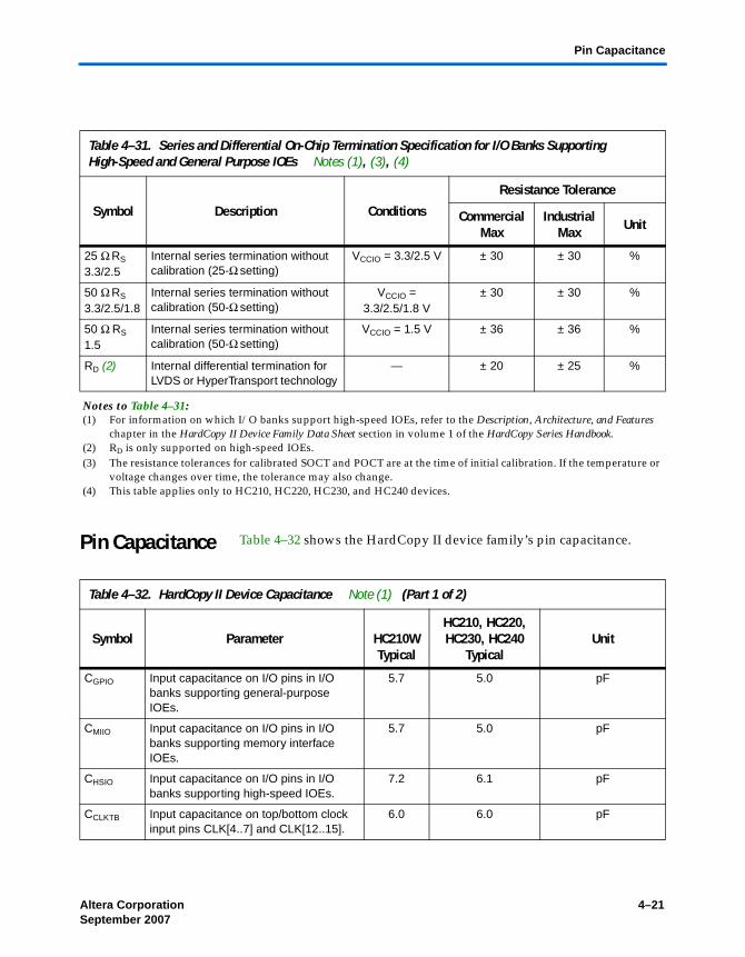
Altera Corporation 4–21September 2007
Pin Capacitance
Pin Capacitance Table 4–32 shows the HardCopy II device family’s pin capacitance.
Table 4–31. Series and Differential On-Chip Termination Specification for I/O Banks Supporting High-Speed and General Purpose IOEs Notes (1), (3), (4)
Symbol Description Conditions
Resistance Tolerance
Commercial Max
Industrial Max Unit
25 Ω RS 3.3/2.5
Internal series termination without calibration (25-Ω setting)
VCCIO = 3.3/2.5 V ± 30 ± 30 %
50 Ω RS 3.3/2.5/1.8
Internal series termination without calibration (50-Ω setting)
VCCIO = 3.3/2.5/1.8 V
± 30 ± 30 %
50 Ω RS 1.5
Internal series termination without calibration (50-Ω setting)
VCCIO = 1.5 V ± 36 ± 36 %
RD (2) Internal differential termination for LVDS or HyperTransport technology
— ± 20 ± 25 %
Notes to Table 4–31:(1) For information on which I/O banks support high-speed IOEs, refer to the Description, Architecture, and Features
chapter in the HardCopy II Device Family Data Sheet section in volume 1 of the HardCopy Series Handbook.(2) RD is only supported on high-speed IOEs.(3) The resistance tolerances for calibrated SOCT and POCT are at the time of initial calibration. If the temperature or
voltage changes over time, the tolerance may also change.(4) This table applies only to HC210, HC220, HC230, and HC240 devices.
Table 4–32. HardCopy II Device Capacitance Note (1) (Part 1 of 2)
Symbol Parameter HC210WTypical
HC210, HC220, HC230, HC240
TypicalUnit
CGPIO Input capacitance on I/O pins in I/O banks supporting general-purpose IOEs.
5.7 5.0 pF
CMIIO Input capacitance on I/O pins in I/O banks supporting memory interface IOEs.
5.7 5.0 pF
CHSIO Input capacitance on I/O pins in I/O banks supporting high-speed IOEs.
7.2 6.1 pF
CCLKTB Input capacitance on top/bottom clock input pins CLK[4..7] and CLK[12..15].
6.0 6.0 pF

4–22 Altera CorporationSeptember 2007
HardCopy Series Handbook, Volume 1
Maximum Input Clock Rates
Tables 4–33 and 4–34 show the maximum input clocking rates of HardCopy II I/Os.
CCLKLR Input capacitance on left/right clock inputs CLK0, CLK2, CLK8, CLK10.
4.3 6.1 pF
CCLKLR+ Input capacitance on left/right clock inputs CLK1, CLK3, CLK9, and CLK11.
4.2 3.3 pF
COUTFB Input capacitance on dual-purpose clock output/feedback pins in PLL banks 9, 10, 11, and 12.
6.9 6.7 pF
Note to Table 4–32:(1) Capacitance is sample-tested only. Capacitance is measured using time-domain reflections (TDR). Measurement
accuracy is within ± 0.5 pF.
Table 4–32. HardCopy II Device Capacitance Note (1) (Part 2 of 2)
Symbol Parameter HC210WTypical
HC210, HC220, HC230, HC240
TypicalUnit
Table 4–33. HardCopy II Maximum Input Clock Rates of HC210, HC220, HC230 and HC240 Devices (Part 1 of 2)
I/OStandardMemory Interface
IOEs
High Speed IOEs
General Purpose
IOEs
CLK [0..3, 8..11]
CLK [4..7,
12..15]FPLL_CLK PLL_FB Unit
LVTTL 500 500 500 500 500 500 500 MHz
2.5 V 500 500 500 500 500 500 500 MHz
1.8 V 500 500 500 500 500 500 500 MHz
1.5 V 500 500 500 500 500 500 500 MHz
LVCMOS 500 500 500 500 500 500 500 MHz
SSTL2 class I 500 — — — 500 — 500 MHz
SSTL2 class II 500 — — — 500 — 500 MHz
SSTL18 class I 500 — — — 500 — 500 MHz
SSTL18 class II 500 — — — 500 — 500 MHz
1.5 V HSTL class I 500 — — — 500 — 500 MHz
1.5 V HSTL class II 500 — — — 500 — 500 MHz
1.8 V HSTL class I 500 — — — 500 — 500 MHz
1.8 V HSTL class II 500 — — — 500 — 500 MHz
PCI (1) 500 — 500 — 500 — 500 MHz

Altera Corporation 4–23September 2007
Maximum Input Clock Rates
PCI-X (1) 500 — 500 — 500 — 500 MHz
Differential SSTL2 class I (2), (3)
500 — — — 500 — 500 MHz
Differential SSTL2 class II (2), (3)
500 — — — 500 — 500 MHz
Differential SSTL18 class I (2), (3)
500 — — — 500 — 500 MHz
Differential SSTL18 class II (2), (3)
500 — — — 500 — 500 MHz
1.8-V Differential HSTL class I (2), (3)
500 — — — 500 — 500 MHz
1.8-V Differential HSTL class II (2), (3)
500 — — — 500 — 500 MHz
1.5-V Differential HSTL class I (2), (3)
500 — — — 500 — 500 MHz
1.5-V Differential HSTL class II (2), (3)
500 — — — 500 — 500 MHz
LVDS — 520 — 717 450 717 450 MHz
LVPECL — — — — 450 — 450 MHz
HyperTransport — 520 — 717 — 717 — MHz
Notes to Table 4–33:(1) The PCI clamping diode is only supported on the top and bottom I/O pins.(2) This I/O standard is only supported on the DQS, CLK, and PLL_FB input pins.(3) For HC210 and HC220, differential HSTL/SSTL input is supported on top/bottom PLL_FB, the top clock pins and
DQS pins located on the top I/Os.
Table 4–33. HardCopy II Maximum Input Clock Rates of HC210, HC220, HC230 and HC240 Devices (Part 2 of 2)
I/OStandardMemory Interface
IOEs
High Speed IOEs
General Purpose
IOEs
CLK [0..3, 8..11]
CLK [4..7,
12..15]FPLL_CLK PLL_FB Unit

4–24 Altera CorporationSeptember 2007
HardCopy Series Handbook, Volume 1
Table 4–34. HardCopy II Maximum Input Clock Rates of HC210W Devices Note (3) (Part 1 of 2)
I/O StandardMemory Interface
IOEs
High Speed IOEs
General Purpose
IOEs
CLK [0..3, 8..11]
CLK [4..7,
12..15]
FPLL_CLK PLL_FB Unit
LVTTL 350 350 350 350 350 350 350 MHz
2.5-V LVTTL/LVCMOS 350 350 350 350 350 350 350 MHz
1.8-V LVTTL/LVCMOS 350 350 350 350 350 350 350 MHz
1.5-V LVTTL/LVCMOS 270 270 270 270 270 270 270 MHz
LVCMOS 350 350 350 350 350 350 350 MHz
SSTL2 class I 350 — — — 350 — 350 MHz
SSTL2 class II 350 — — — 350 — 350 MHz
SSTL18 class I 350 — — — 350 — 350 MHz
SSTL18 class II 350 — — — 350 — 350 MHz
1.5-V HSTL class I 350 — — — 350 — 350 MHz
1.5-V HSTL class II 350 — — — 350 — 350 MHz
1.8-V HSTL class I 350 — — — 350 — 350 MHz
1.8-V HSTL class II 350 — — — 350 — 350 MHz
PCI (1) 315 — 315 — 315 — 315 MHz
PCI-X (1) 315 — 315 — 315 — 315 MHz
Differential SSTL2 class I (2) — — — — 350 — 350 MHz
Differential SSTL2 class II (2) — — — — 350 — 350 MHz
Differential SSTL18 class I (2) — — — — 350 — 350 MHz
Differential SSTL18 class II (2) — — — — 350 — 350 MHz
1.8-V differential HSTL class I (2)
— — — — 350 — 350 MHz
1.8-V differential HSTL class II (2)
— — — — 350 — 350 MHz
1.5-V differential HSTL class I (2)
— — — — 350 — 350 MHz
1.5-V differential HSTL class II (2)
— — — — 350 — 350 MHz
LVDS — 320 — 320 320 320 320 MHz
LVPECL — — — — 320 — 320 MHz

Altera Corporation 4–25September 2007
Maximum Output Clock Rates
Maximum Output Clock Rates
Tables 4–35 and 4–36 show the maximum output toggle rates of HardCopy II I/O's for all available drive strengths.
HyperTransport — 320 — 320 — 320 — MHz
Notes to Table 4–34:(1) The PCI clamping diode is only supported on the top and bottom I/O pins.(2) For HC210W, differential HSTL/SSTL input is supported on the top clock pins, the DQS pins on the top I/O banks and
top/bottom PLL_FB input pins.(3) These numbers are preliminary and pending further silicon characterization.
Table 4–34. HardCopy II Maximum Input Clock Rates of HC210W Devices Note (3) (Part 2 of 2)
I/O StandardMemory Interface
IOEs
High Speed IOEs
General Purpose
IOEs
CLK [0..3, 8..11]
CLK [4..7,
12..15]
FPLL_CLK PLL_FB Unit
Table 4–35. HardCopy II Maximum Output Clock Rate of HC210, HC220, HC230 and HC240 Devices Note (1) (Part 1 of 5)
I/O Standard Drive Strength
Memory Interface
IOEs
High Speed IOEs
General Purpose IOEs CLK [0,
2, 8, 10] (2)
CLK [4..7,
12..15]PLL_OUT Unit
Bottom Column
Right Row
3.3-V LVTTL 4 mA 225 225 225 225 225 225 225 MHz
8 mA 355 355 355 355 355 355 355 MHz
12 mA 475 475 475 475 475 475 475 MHz
16 mA 594 — — — — 594 594 MHz
20 mA 700 — — — — 700 700 MHz
24 mA (3) 794 — — — — 794 794 MHz
3.3-V LVCMOS 4 mA 250 250 250 250 250 250 250 MHz
8 mA 480 480 480 480 480 480 480 MHz
12 mA 710 — — — — 710 710 MHz
16 mA 925 — — — — 925 925 MHz
20 mA 985 — — — — 985 985 MHz
24 mA (3) 1040 — — — — 1040 1040 MHz

4–26 Altera CorporationSeptember 2007
HardCopy Series Handbook, Volume 1
2.5-VLVTTL / LVCMOS
4 mA 194 194 194 194 194 194 194 MHz
8 mA 380 380 380 380 380 380 380 MHz
12 mA 575 575 575 575 575 575 575 MHz
16 mA (3) 845 — — — — 845 845 MHz
1.8-VLVTTL / LVCMOS
2 mA 109 109 109 109 109 109 109 MHz
4 mA 250 250 250 250 250 250 250 MHz
6 mA 390 390 390 390 390 390 390 MHz
8 mA 570 570 570 570 570 570 570 MHz
10 mA 805 — — — — 805 805 MHz
12 mA (3) 1040 — — — — 1040 1040 MHz
1.5-VLVTTL / LVCMOS
2 mA 200 200 200 200 200 200 200 MHz
4 mA 370 370 370 370 370 370 370 MHz
6 mA 430 — — — — 430 430 MHz
8 mA (3) 495 — — — — 495 495 MHz
SSTL2 class I
8 mA 300 — — — — 300 300 MHz
12 mA (3) 400 — — — — 400 400 MHz
SSTL2 class II
16 mA 350 — — — — 350 350 MHz
20 mA 350 — — — — 350 350 MHz
24 mA (3) 400 — — — — 400 400 MHz
SSTL18 class I
4 mA 150 — — — — 150 150 MHz
6 mA 250 — — — — 250 250 MHz
8 mA 300 — — — — 300 300 MHz
10 mA 400 — — — — 400 400 MHz
12 mA (3) 550 — — — — 550 550 MHz
SSTL18 class II
8 mA 200 — — — — 200 200 MHz
16 mA 350 — — — — 350 350 MHz
18 mA 400 — — — — 400 400 MHz
20 mA (3) 500 — — — — 500 500 MHz
Table 4–35. HardCopy II Maximum Output Clock Rate of HC210, HC220, HC230 and HC240 Devices Note (1) (Part 2 of 5)
I/O Standard Drive Strength
Memory Interface
IOEs
High Speed IOEs
General Purpose IOEs CLK [0,
2, 8, 10] (2)
CLK [4..7,
12..15]PLL_OUT Unit
Bottom Column
Right Row

Altera Corporation 4–27September 2007
Maximum Output Clock Rates
1.8-V HSTL class I
4 mA 300 — — — — 300 300 MHz
6 mA 450 — — — — 450 450 MHz
8 mA 600 — — — — 600 600 MHz
10 mA 650 — — — — 650 650 MHz
12 mA (3) 700 — — — — 700 700 MHz
1.8-V HSTL class II
16 mA 500 — — — — 500 500 MHz
18 mA 500 — — — — 500 500 MHz
20 mA (3) 550 — — — — 550 550 MHz
1.5-V HSTL class I
4 mA 300 — — — — 300 300 MHz
6 mA 500 — — — — 500 500 MHz
8 mA 650 — — — — 650 650 MHz
10 mA 700 — — — — 700 700 MHz
12 mA (3) 700 — — — — 700 700 MHz
1.5-V HSTL class II
16 mA 600 — — — — 600 600 MHz
18 mA 600 — — — — 600 600 MHz
20 mA (3) 650 — — — — 650 650 MHz
PCI (4) — 790 — 790 — — 790 790 MHz
PCI-X (4) — 790 — 790 — — 790 790 MHz
LVDS — — 717 — — — — 400 MHz
HyperTransport — — 717 — — — — — MHz
LVPECL — — — — — — — 400 MHz
Differential SSTL2 class I (5)
8 mA 300 — — — — 300 300 MHz
12 mA (3) 400 — — — — 400 400 MHz
Differential SSTL2 class II (5)
16 mA 350 — — — — 350 350 MHz
20 mA (3) 350 — — — — 350 350 MHz
24 mA (3) 400 — — — — 400 400 MHz
Table 4–35. HardCopy II Maximum Output Clock Rate of HC210, HC220, HC230 and HC240 Devices Note (1) (Part 3 of 5)
I/O Standard Drive Strength
Memory Interface
IOEs
High Speed IOEs
General Purpose IOEs CLK [0,
2, 8, 10] (2)
CLK [4..7,
12..15]PLL_OUT Unit
Bottom Column
Right Row

4–28 Altera CorporationSeptember 2007
HardCopy Series Handbook, Volume 1
Differential SSTL18 class I (5)
4 mA 150 — — — — 150 150 MHz
6 mA 250 — — — — 250 250 MHz
8 mA 300 — — — — 300 300 MHz
10 mA 400 — — — — 400 400 MHz
12 mA (3) 550 — — — — 550 550 MHz
Differential SSTL18 class II (5)
8 mA 200 — — — — 200 200 MHz
16 mA 350 — — — — 350 350 MHz
18 mA 400 — — — — 400 400 MHz
20 mA (3) 500 — — — — 500 500 MHz
1.8-V differential HSTL class I(5)
4 mA 300 — — — — 300 300 MHz
6 mA 450 — — — — 450 450 MHz
8 mA 600 — — — — 600 600 MHz
10 mA 650 — — — — 650 650 MHz
12 mA (3) 700 — — — — 700 700 MHz
1.8-V differential HSTL class II(5)
16 mA 500 — — — — 500 500 MHz
18 mA 500 — — — — 500 500 MHz
20 mA (3) 550 — — — — 550 550 MHz
1.5-V differential HSTL class I(5)
4 mA 300 — — — — 300 300 MHz
6 mA 500 — — — — 500 500 MHz
8 mA 650 — — — — 650 650 MHz
10 mA 700 — — — — 700 700 MHz
12 mA (3) 700 — — — — 700 700 MHz
Table 4–35. HardCopy II Maximum Output Clock Rate of HC210, HC220, HC230 and HC240 Devices Note (1) (Part 4 of 5)
I/O Standard Drive Strength
Memory Interface
IOEs
High Speed IOEs
General Purpose IOEs CLK [0,
2, 8, 10] (2)
CLK [4..7,
12..15]PLL_OUT Unit
Bottom Column
Right Row

Altera Corporation 4–29September 2007
Maximum Output Clock Rates
1.5-V differential HSTL class II (5)
16 mA 600 — — — — 600 600 MHz
18 mA 600 — — — — 600 600 MHz
20 mA (3) 650 — — — — 650 650 MHz
Notes to Table 4–35:(1) The toggle rate applies to 0 pF output load for all I/O standards except for LVDS and HyperTransport technology
on row I/O pins. For LVDS and HyperTransport technology on row I/O pins, the toggle rates apply to load from 0 to 5 pF.
(2) CLK [1, 3, 9, 11] and FPLL_CLK are dedicated input clocks, and are excluded from this table.
(3) This is the default setting in the Quartus® II software if supported by the pin location.(4) The PCI clamping diode is only supported on the top and bottom I/O pins.(5) Like Stratix II devices, differential HSTL and SSTL is supported only on the column CLK, PLL_OUT and memory
interface DQS IOE pins. For HC210 and HC220, only the top column clock pins support Differential HSTL and SSTL.
Table 4–35. HardCopy II Maximum Output Clock Rate of HC210, HC220, HC230 and HC240 Devices Note (1) (Part 5 of 5)
I/O Standard Drive Strength
Memory Interface
IOEs
High Speed IOEs
General Purpose IOEs CLK [0,
2, 8, 10] (2)
CLK [4..7,
12..15]PLL_OUT Unit
Bottom Column
Right Row
Table 4–36. HardCopy II Maximum Output Clock Rate for HC210W Devices Notes (1), (6) (Part 1 of 4)
I/O Standard Drive Strength
Memory Interface
IOEs
High Speed IOEs
General Purpose IOEs CLK [0,
2, 8, 10] (2)
CLK [4..7,
12..15]PLL_OUT Unit
Bottom Column
Right Row
3.3-V LVTTL 4 mA 100 100 100 100 100 100 100 MHz
8 mA 170 170 170 170 170 170 170 MHz
12 mA 230 230 230 230 230 230 230 MHz
16 mA 240 — — — — 240 240 MHz
20 mA 280 — — — — 280 280 MHz
24 mA (3) 300 — — — — 300 300 MHz
3.3-V LVCMOS 4 mA 175 175 175 175 175 175 175 MHz
8 mA 230 230 230 230 230 230 230 MHz
12 mA 260 — — — — 260 260 MHz
16 mA 270 — — — — 270 270 MHz
20 mA 290 — — — — 290 290 MHz
24 mA (3) 310 — — — — 310 310 MHz

4–30 Altera CorporationSeptember 2007
HardCopy Series Handbook, Volume 1
2.5-VLVTTL / LVCMOS
4 mA 136 136 136 136 136 136 136 MHz
8 mA 230 230 230 230 230 230 230 MHz
12 mA 370 370 370 370 370 370 370 MHz
16 mA (3) 405 — — — — 405 405 MHz
1.8-VLVTTL / LVCMOS
2 mA 77 77 77 77 77 77 77 MHz
4 mA 150 150 150 150 150 150 150 MHz
6 mA 180 180 180 180 180 180 180 MHz
8 mA 200 200 200 200 200 200 200 MHz
10 mA 250 — — — — 250 250 MHz
12 mA (3) 290 — — — — 290 290 MHz
1.5-VLVTTL / LVCMOS
2 mA 60 60 60 60 60 60 60 MHz
4 mA 110 110 110 110 110 110 110 MHz
6 mA 150 — — — — 150 150 MHz
8 mA (3) 190 — — — — 190 190 MHz
SSTL2 class I 8 mA 210 — — — — 210 210 MHz
12 mA (3) 280 — — — — 280 280 MHz
SSTL2 class II 16 mA 245 — — — — 245 245 MHz
20 mA 245 — — — — 245 245 MHz
24 mA (3) 280 — — — — 280 280 MHz
SSTL18 class I 4 mA 105 — — — — 105 105 MHz
6 mA 175 — — — — 175 175 MHz
8 mA 210 — — — — 210 210 MHz
10 mA 220 — — — — 220 220 MHz
12 mA (3) 230 — — — — 230 230 MHz
SSTL18 class II 8 mA 140 — — — — 140 140 MHz
16 mA 220 — — — — 220 220 MHz
18 mA 220 — — — — 220 220 MHz
20 mA (3) 350 — — — — 350 350 MHz
Table 4–36. HardCopy II Maximum Output Clock Rate for HC210W Devices Notes (1), (6) (Part 2 of 4)
I/O Standard Drive Strength
Memory Interface
IOEs
High Speed IOEs
General Purpose IOEs CLK [0,
2, 8, 10] (2)
CLK [4..7,
12..15]PLL_OUT Unit
Bottom Column
Right Row

Altera Corporation 4–31September 2007
Maximum Output Clock Rates
1.8-V HSTL class I 4 mA 210 — — — — 210 210 MHz
6 mA 210 — — — — 210 210 MHz
8 mA 220 — — — — 220 220 MHz
10 mA 250 — — — — 250 250 MHz
12 mA (3) 270 — — — — 270 270 MHz
1.8-V HSTL class II
16 mA 190 — — — — 190 190 MHz
18 mA 200 — — — — 200 200 MHz
20 mA (3) 210 — — — — 210 210 MHz
1.5-V HSTL class I 4 mA 150 — — — — 150 150 MHz
6 mA 160 — — — — 160 160 MHz
8 mA 170 — — — — 170 170 MHz
10 mA 180 — — — — 180 180 MHz
12 mA (3) 190 — — — — 190 190 MHz
1.5-V HSTL class II
16 mA 170 — — — — 170 170 MHz
18 mA 170 — — — — 170 170 MHz
20 mA (3) 170 — — — — 170 170 MHz
PCI (4) — 315 — 315 — — 315 315 MHz
PCI-X (4) — 315 — 315 — — 315 315 MHz
LVDS — — 320 — — — — 280 MHz
HyperTransport — — 320 — — — — — MHz
LVPECL — — — — — — — 280 MHz
Differential SSTL2 class I (5)
8 mA 210 — — — — 210 210 MHz
12 mA (3) 280 — — — — 280 280 MHz
Differential SSTL2 class II (5)
16 mA 245 — — — — 245 245 MHz
20 mA 245 — — — — 245 245 MHz
24 mA (3) 280 — — — — 280 280 MHz
Differential SSTL18 class I (5)
4 mA 105 — — — — 105 105 MHz
6 mA 175 — — — — 175 175 MHz
8 mA 210 — — — — 210 210 MHz
10 mA 220 — — — — 220 220 MHz
12 mA (3) 230 — — — — 230 230 MHz
Table 4–36. HardCopy II Maximum Output Clock Rate for HC210W Devices Notes (1), (6) (Part 3 of 4)
I/O Standard Drive Strength
Memory Interface
IOEs
High Speed IOEs
General Purpose IOEs CLK [0,
2, 8, 10] (2)
CLK [4..7,
12..15]PLL_OUT Unit
Bottom Column
Right Row

4–32 Altera CorporationSeptember 2007
HardCopy Series Handbook, Volume 1
Differential SSTL18 class II (5)
8 mA 140 — — — — 140 140 MHz
16 mA 220 — — — — 220 220 MHz
18 mA 220 — — — — 220 220 MHz
20 mA (3) 220 — — — — 220 220 MHz
1.8-V differential HSTL class I (5)
4 mA 210 — — — — 210 210 MHz
6 mA 210 — — — — 210 210 MHz
8 mA 220 — — — — 220 220 MHz
10 mA 250 — — — — 250 250 MHz
12 mA (3) 270 — — — — 270 270 MHz
1.8-V differential HSTL class II (5)
16 mA 190 — — — — 190 190 MHz
18 mA 200 — — — — 200 200 MHz
20 mA (3) 210 — — — — 210 210 MHz
1.5-V differential HSTL class I (5)
4 mA 150 — — — — 150 150 MHz
6 mA 160 — — — — 160 160 MHz
8 mA 170 — — — — 170 170 MHz
10 mA 180 — — — — 180 180 MHz
12 mA (3) 190 — — — — 190 190 MHz
1.5-V differential HSTL class II (5)
16 mA 170 — — — — 170 170 MHz
18 mA 170 — — — — 170 170 MHz
20 mA (3) 170 — — — — 170 170 MHz
Notes to Table 4–36:(1) The toggle rate applies to 0 pF output load for all I/O standards except for LVDS and HyperTransport technology on
row I/O pins. For LVDS and HyperTransport technology on row I/O pins, the toggle rates apply to load from 0 to 5 pF.
(2) CLK [1, 3, 9, 11] and FPLL_CLK are dedicated input clocks, and excluded from this table.(3) This is the default setting in the Quartus II software if supported by the pin location.(4) The PCI clamping diode is only supported on the top and bottom I/O pins.(5) Like Stratix II devices, differential HSTL and SSTL is supported only on the column CLK, PLL_OUT and memory
interface DQS IOE pins. For HC210 and HC220, only the top column clock pins support Differential HSTL and SSTL.(6) These numbers are preliminary and pending further silicon characterization.
Table 4–36. HardCopy II Maximum Output Clock Rate for HC210W Devices Notes (1), (6) (Part 4 of 4)
I/O Standard Drive Strength
Memory Interface
IOEs
High Speed IOEs
General Purpose IOEs CLK [0,
2, 8, 10] (2)
CLK [4..7,
12..15]PLL_OUT Unit
Bottom Column
Right Row

Altera Corporation 4–33September 2007
Maximum Output Clock Rates
Tables 4–37 and 4–38 show the maximum output toggle rates of HardCopy II I/Os using OCT.
Table 4–37. HardCopy II Maximum Output Clock Rate for HC210, HC220, HC230 and HC240 Devices (OCT)Note (1) (Part 1 of 2)
I/O Standard Drive Strength
Memory Interface
IOEs
High Speed IOEs
General Purpose IOEs CLK [0,
2, 8, 10] (2)
CLK [4..7,
12..15]PLL_OUT Unit
Bottom Column
Right Row
3.3-V LVTTL OCT 50 Ω 400 400 400 400 400 400 400 MHz
2.5-V LVTTL OCT 50 Ω 350 350 350 350 350 350 350 MHz
1.8-V LVTTL OCT 50 Ω 550 550 550 550 550 550 550 MHz
3.3-V LVCMOS OCT 50 Ω 350 350 350 350 350 350 350 MHz
1.5-V LVCMOS OCT 50 Ω 450 450 450 450 450 450 450 MHz
SSTL-2 Class I OCT 50 Ω 500 — — — — 500 500 MHz
SSTL-2 Class II OCT 25 Ω 550 — — — — 550 550 MHz
SSTL-18 Class I OCT 50 Ω 400 — — — — 400 400 MHz
SSTL-18 Class II OCT 25 Ω 500 — — — — 500 500 MHz
1.5-V HSTL Class I
OCT 50 Ω 550 — — — — 550 550 MHz
1.8-V HSTL Class I
OCT 50 Ω 600 — — — — 600 600 MHz
1.8-V HSTL Class II
OCT 50 Ω 500 — — — — 500 500 MHz
Differential SSTL-2 Class I (3)
OCT 50 Ω 500 — — — — 500 500 MHz
Differential SSTL-2 Class II (3)
OCT 25 Ω 550 — — — — 550 550 MHz
Differential SSTL-18 Class I (3)
OCT 50 Ω 400 — — — — 400 400 MHz
Differential SSTL-18 Class II (3)
OCT 25 Ω 500 — — — — 500 500 MHz
1.8-V Differential HSTL Class I (3)
OCT 50 Ω 600 — — — — 600 600 MHz
1.8-V Differential HSTL Class II (3)
OCT 25 Ω 500 — — — — 500 500 MHz

4–34 Altera CorporationSeptember 2007
HardCopy Series Handbook, Volume 1
1.5-V Differential HSTL Class I (3)
OCT 50 Ω 550 — — — — 550 550 MHz
Notes to Table 4–37:(1) The toggle rate applies to 0 pF output load for all I/O standards except for LVDS and HyperTransport technology
on row I/O pins. For LVDS and HyperTransport technology on row I/O pins, the toggle rates apply to load from 0 to 5 pF.
(2) CLK [1, 3, 9, 11] and FPLL_CLK are dedicated input clocks, and excluded from this table.(3) Like Stratix II devices, differential HSTL and SSTL is supported only on the column CLK, PLL_OUT and memory
interface DQS IOE pins. For HC210 and HC220, only the top column clock pins support Differential HSTL and SSTL.
Table 4–37. HardCopy II Maximum Output Clock Rate for HC210, HC220, HC230 and HC240 Devices (OCT)Note (1) (Part 2 of 2)
I/O Standard Drive Strength
Memory Interface
IOEs
High Speed IOEs
General Purpose IOEs CLK [0,
2, 8, 10] (2)
CLK [4..7,
12..15]PLL_OUT Unit
Bottom Column
Right Row
Table 4–38. HardCopy II Maximum Output Clock Rate for HC210W using OCT Notes (1), (4) (Part 1 of 2)
I/O Standard Drive Strength
Memory Interface
IOEs
High Speed IOEs
General Purpose IOEs CLK [0,
2, 8, 10] (2)
CLK [4..7,
12..15]PLL_OUT Unit
Bottom Column
Right Row
3.3-V LVTTL OCT 50 Ω 280 280 280 280 280 280 280 MHz
2.5-V LVTTL OCT 50 Ω 245 245 245 245 245 245 245 MHz
1.8-V LVTTL OCT 50 Ω 290 290 290 290 290 290 290 MHz
3.3-V LVCMOS OCT 50 Ω 245 245 245 245 245 245 245 MHz
1.5-V LVCMOS OCT 50 Ω 190 190 190 190 190 190 190 MHz
SSTL-2 Class I OCT 50 Ω 280 — — — — 280 280 MHz
SSTL-2 Class II OCT 25 Ω 280 — — — — 280 280 MHz
SSTL-18 Class I OCT 50 Ω 230 — — — — 230 230 MHz
SSTL-18 Class II OCT 25 Ω 220 — — — — 220 220 MHz
1.5-V HSTL Class I
OCT 50 Ω 190 — — — — 190 190 MHz
1.8-V HSTL Class I
OCT 50 Ω 270 — — — — 270 270 MHz
1.8-V HSTL Class II
OCT 50 Ω 210 — — — — 210 210 MHz
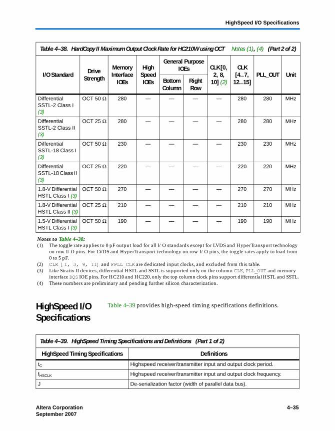
Altera Corporation 4–35September 2007
HighSpeed I/O Specifications
HighSpeed I/O Specifications
Table 4–39 provides high-speed timing specifications definitions.
Differential SSTL-2 Class I (3)
OCT 50 Ω 280 — — — — 280 280 MHz
Differential SSTL-2 Class II (3)
OCT 25 Ω 280 — — — — 280 280 MHz
Differential SSTL-18 Class I (3)
OCT 50 Ω 230 — — — — 230 230 MHz
Differential SSTL-18 Class II (3)
OCT 25 Ω 220 — — — — 220 220 MHz
1.8-V Differential HSTL Class I (3)
OCT 50 Ω 270 — — — — 270 270 MHz
1.8-V Differential HSTL Class II (3)
OCT 25 Ω 210 — — — — 210 210 MHz
1.5-V Differential HSTL Class I (3)
OCT 50 Ω 190 — — — — 190 190 MHz
Notes to Table 4–38:(1) The toggle rate applies to 0 pF output load for all I/O standards except for LVDS and HyperTransport technology
on row I/O pins. For LVDS and HyperTransport technology on row I/O pins, the toggle rates apply to load from 0 to 5 pF.
(2) CLK [1, 3, 9, 11] and FPLL_CLK are dedicated input clocks, and excluded from this table.(3) Like Stratix II devices, differential HSTL and SSTL is supported only on the column CLK, PLL_OUT and memory
interface DQS IOE pins. For HC210 and HC220, only the top column clock pins support differential HSTL and SSTL.(4) These numbers are preliminary and pending further silicon characterization.
Table 4–38. HardCopy II Maximum Output Clock Rate for HC210W using OCT Notes (1), (4) (Part 2 of 2)
I/O Standard Drive Strength
Memory Interface
IOEs
High Speed IOEs
General Purpose IOEs CLK [0,
2, 8, 10] (2)
CLK [4..7,
12..15]PLL_OUT Unit
Bottom Column
Right Row
Table 4–39. HighSpeed Timing Specifications and Definitions (Part 1 of 2)
HighSpeed Timing Specifications Definitions
tC Highspeed receiver/transmitter input and output clock period.
fHSCLK Highspeed receiver/transmitter input and output clock frequency.
J De-serialization factor (width of parallel data bus).

4–36 Altera CorporationSeptember 2007
HardCopy Series Handbook, Volume 1
Table 4–40 shows the high-speed I/O timing specifications for HC210W F484 WireBond devices.
W PLL multiplication factor
tRISE Low-to-high transmission time.
tFALL High-to-low transmission time.
Timing unit interval (TUI) The timing budget allowed for skew, propagation delays, and data sampling window. (TUI = 1/(Receiver Input Clock Frequency × Multiplication Factor) = tC/w).
fHSDR Maximum/minimum LVDS data transfer rate (fHSDR = 1/TUI), non-DPA.
fHSDRDPA Maximum/minimum LVDS data transfer rate (fHSDRDPA = 1/TUI), DPA.
Channel-to-channel skew (TCCS) The timing difference between the fastest and slowest output edges, including tCO variation and clock skew. The clock is included in the TCCS measurement.
Sampling window (SW) The period of time during which the data must be valid in order to capture it correctly. The setup and hold times determine the ideal strobe position within the sampling window.
Input jitter (peak-to-peak) Peak-to-peak input jitter on highspeed PLLs.
Output jitter (peak-to-peak) Peak-to-peak output jitter on highspeed PLLs.
tDUTY Duty cycle on highspeed transmitter output clock.
tLOCK Lock time for highspeed transmitter and receiver PLLs.
Table 4–39. HighSpeed Timing Specifications and Definitions (Part 2 of 2)
HighSpeed Timing Specifications Definitions
Table 4–40. HardCopy II High-Speed I/O Specifications for HC210W Device Notes (1), (2) (Part 1 of 2)
Symbol Conditions Min Typ Max Unit
fHSCLK (clock frequency) fHSCLK = fHSDR / W
W = 2 to 32 (LVDS, HyperTransport technology) (3)
16 — 320 MHz
W = 1 (SERDES bypass, LVDS only) 16 — 320 MHz
W = 1 (SERDES used, LVDS only) 150 — 320 MHz
fHSDR (data rate) J = 4 to 10 (LVDS, HyperTransport technology) 150 — 640 Mbps
J = 2 (LVDS, HyperTransport technology) (4) — 640 Mbps
J = 1 t(LVDS only) (4) — 320 Mbps
fHSDRDPA (DPA data rate) J = 4 to 10 (LVDS, HyperTransport technology) 150 — 640 Mbps
TCCS All differential standards — — 240 ps
SW All differential standards 400 — — ps
Output jitter — — — (5) ps

Altera Corporation 4–37September 2007
HighSpeed I/O Specifications
Table 4–41 shows the high-speed I/O timing specifications for HC210, HC220, HC230 and HC240 HardCopy II devices.
Output tRISE All differential I/O standards — — (5) ps
Output tFALL All differential I/O standards — — (5) ps
tDUTY — — — 45 50 55 %
DPA run length — — — — — 6,400 UI
DPA jitter tolerance (peak-to-peak)
— — — (5) — — UI
DPA lock time Standard Training Pattern
Transition Density
— — — Number of repetitions
— — — — — —
SPI4 00000000001111111111
10% (5) — —
Parallel Rapid I/O 10010000 25% (5) — —
— 10010000 50% (5) — —
Miscellaneous 10101010 100% (5) — —
— 10101010 — (5) — —
Notes to Table 4–40:(1) These numbers are preliminary and pending further silicon characterization.(2) When J = 4 to 10, the SERDES block is used.
When J = 1 or 2, the SERDES block is bypassed.(3) The input clock frequency and the W factor must satisfy the following fast PLL VCO specification: 150 ≤ input clock
frequency × W ≤ 640.(4) The minimum specification is dependent on the clock source (fast PLL, enhanced PLL, clock pin, and so on) and
the clock routing resource (global, regional, or local) used. The I/O differential buffer and input register do not have a minimum toggle rate.
(5) Contact the Altera Applications Group for more information.
Table 4–40. HardCopy II High-Speed I/O Specifications for HC210W Device Notes (1), (2) (Part 2 of 2)
Symbol Conditions Min Typ Max Unit
Table 4–41. HardCopy II High-Speed I/O Specifications for HC210, HC220, HC230 and HC240 Devices Note (1) (Part 1 of 2)
Symbol Conditions Min Typ Max Unit
fHSCLK (clock frequency) fHSCLK = fHSDR / W
W = 2 to 32 (LVDS, HyperTransport technology) (2)
16 — 520 MHz
W = 1 (SERDES bypass, LVDS only) 16 — 500 MHz
W = 1 (SERDES used, LVDS only) 150 — 717 MHz
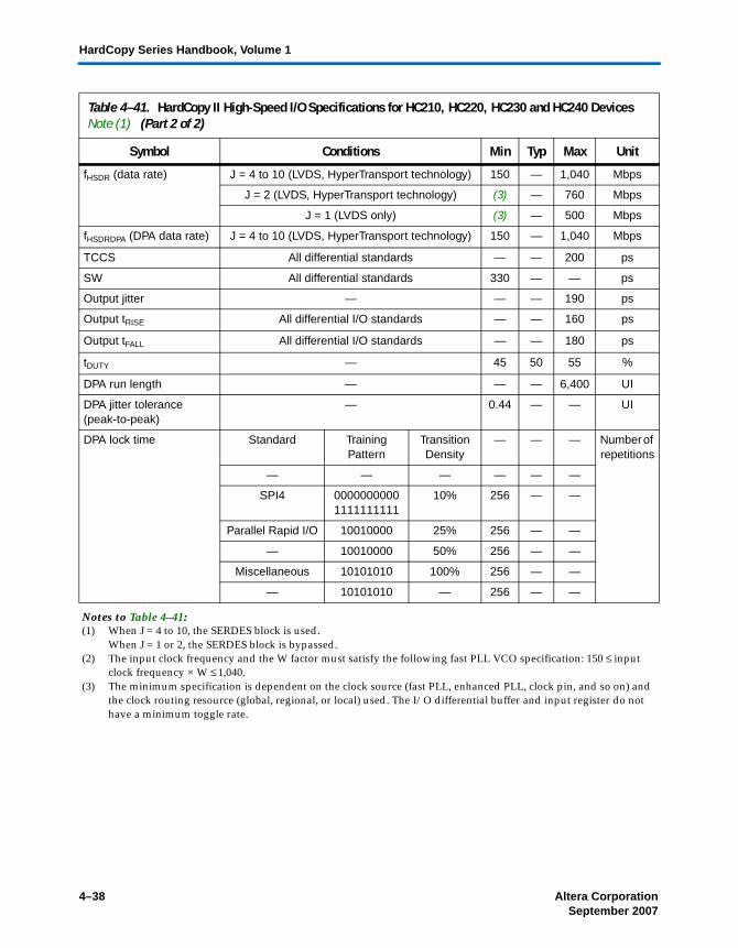
4–38 Altera CorporationSeptember 2007
HardCopy Series Handbook, Volume 1
fHSDR (data rate) J = 4 to 10 (LVDS, HyperTransport technology) 150 — 1,040 Mbps
J = 2 (LVDS, HyperTransport technology) (3) — 760 Mbps
J = 1 (LVDS only) (3) — 500 Mbps
fHSDRDPA (DPA data rate) J = 4 to 10 (LVDS, HyperTransport technology) 150 — 1,040 Mbps
TCCS All differential standards — — 200 ps
SW All differential standards 330 — — ps
Output jitter — — — 190 ps
Output tRISE All differential I/O standards — — 160 ps
Output tFALL All differential I/O standards — — 180 ps
tDUTY — 45 50 55 %
DPA run length — — — 6,400 UI
DPA jitter tolerance(peak-to-peak)
— 0.44 — — UI
DPA lock time Standard Training Pattern
Transition Density
— — — Number of repetitions
— — — — — —
SPI4 00000000001111111111
10% 256 — —
Parallel Rapid I/O 10010000 25% 256 — —
— 10010000 50% 256 — —
Miscellaneous 10101010 100% 256 — —
— 10101010 — 256 — —
Notes to Table 4–41:(1) When J = 4 to 10, the SERDES block is used.
When J = 1 or 2, the SERDES block is bypassed.(2) The input clock frequency and the W factor must satisfy the following fast PLL VCO specification: 150 ≤ input
clock frequency × W ≤1,040.(3) The minimum specification is dependent on the clock source (fast PLL, enhanced PLL, clock pin, and so on) and
the clock routing resource (global, regional, or local) used. The I/O differential buffer and input register do not have a minimum toggle rate.
Table 4–41. HardCopy II High-Speed I/O Specifications for HC210, HC220, HC230 and HC240 Devices Note (1) (Part 2 of 2)
Symbol Conditions Min Typ Max Unit

Altera Corporation 4–39September 2007
PLL Timing Specifications
PLL Timing Specifications
Tables 4–42 and 4–43 describe the HardCopy II PLL specifications when operating in both the commercial junction temperature range (0° to 85° C) and the industrial junction temperature range (–40° to 100° C), except for the clock switchover feature. Like the Stratix II devices, the clock switchover feature is only supported from the 0° to 100° C junction temperature range.
Table 4–42. HardCopy II Enhanced PLL Specifications (Part 1 of 2)
Name Description Min Typ Max Unit
fIN Input clock frequency for HC210, HC220, HC230 and HC240 devices
2 — 500 MHz
Input clock frequency for the HC210W device
2 — 320 (1) MHz
fINPFD Input frequency to the PFD 2 — 420 MHz
fINDUTY Input clock duty cycle 40 — 60 %
fEINDUTY External feedback input clock duty cycle
40 — 60 %
tINJITTER Input or external feedback clock input jitter tolerance in terms of period jitter. Bandwidth ≤ 0.85 MHz
— 0.5 — ns (pp)
Input or external feedback clock input jitter tolerance in terms of period jitter. Bandwidth > 0.85 MHz
— 1 — ns (pp)
tOUTJITTER Dedicated clock output period jitter for HC210, HC220, HC230 and HC240 devices
— — 250 ps for ≥ 100 MHz outclk
25 mUI for < 100 MHz outclk
ps or mUI
Dedicated clock output period jitter for HC210W device
— — 300 ps for ≥ 100 MHz outclk
30 mUI for < 100 MHz outclk
ps or mUI
tFCOMP External feedback compensation time
— — 10 ns
fOUT Output frequency for internal global or regional clock
1.5 (2) — 550 MHz
tOUTDUTY Duty cycle for external clock output (when set to 50%).
45 50 55 %
fSCANCLK Scanclk frequency — — 100 MHz
tCONFIGEPLL Time required to reconfigure scan chains for enhanced PLLs
— 174/fSCANCLK — ns
fOUT_EXT PLL external clock output frequency
1.5 (2) — (1) MHz

4–40 Altera CorporationSeptember 2007
HardCopy Series Handbook, Volume 1
tLOCK Time required for the PLL to lock from the time it is enabled or the end of device configuration
— 0.03 1 ms
tDLOCK Time required for the PLL to lock dynamically after automatic clock switchover between two identical clock frequencies
— — 1 ms
fSWITCHOVER Frequency range where the clock switchover performs properly
4 — 500 MHz
fCLKW PLL closed loop bandwidth 0.13 1.2 16.9 MHz
fVCO PLL VCO operating range for HC210, HC220, HC230 and HC240 devices
300 — 1,040 MHz
PLL VCO operating range for HC210W devices
300 — 840 MHz
fSS Spread spectrum modulation frequency
100 — 500 MHz
% spread Percent down spread for a given clock frequency
0.4 0.5 0.6 %
tPLL_PSERR Accuracy of PLL phase shift — — ± 15 ps
tARESET Minimum pulse width on ARESET signal.
10 (3) — — ns
500 (4) — — ns
tARESET_RECONFIG Minimum pulse width on the areset signal when using PLL reconfiguration. Reset the PLL after scan done goes high.
500 — — ns
Notes to Table 4–42:(1) Limited by I/O fMAX. (2) If the counter cascading feature of the PLL is used, there is no minimum output clock frequency.(3) Applicable when the PLL input clock has been running continuously for at least 10 µs.(4) Applicable when the PLL input clock has stopped toggling or has been running continuously for less than 10 µs.
Table 4–42. HardCopy II Enhanced PLL Specifications (Part 2 of 2)
Name Description Min Typ Max Unit
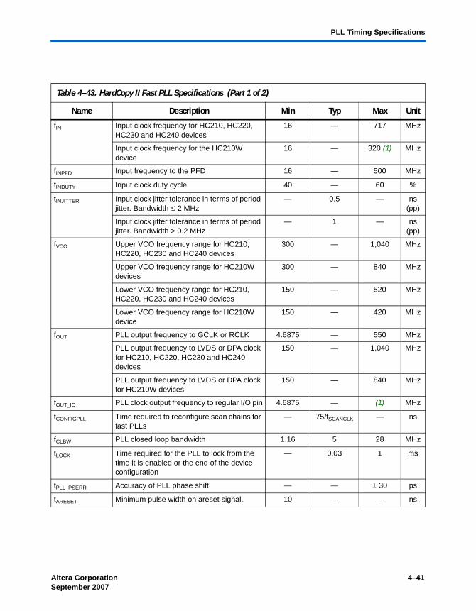
Altera Corporation 4–41September 2007
PLL Timing Specifications
Table 4–43. HardCopy II Fast PLL Specifications (Part 1 of 2)
Name Description Min Typ Max Unit
fIN Input clock frequency for HC210, HC220, HC230 and HC240 devices
16 — 717 MHz
Input clock frequency for the HC210W device
16 — 320 (1) MHz
fINPFD Input frequency to the PFD 16 — 500 MHz
fINDUTY Input clock duty cycle 40 — 60 %
tINJITTER Input clock jitter tolerance in terms of period jitter. Bandwidth ≤ 2 MHz
— 0.5 — ns (pp)
Input clock jitter tolerance in terms of period jitter. Bandwidth > 0.2 MHz
— 1 — ns (pp)
fVCO Upper VCO frequency range for HC210, HC220, HC230 and HC240 devices
300 — 1,040 MHz
Upper VCO frequency range for HC210W devices
300 — 840 MHz
Lower VCO frequency range for HC210, HC220, HC230 and HC240 devices
150 — 520 MHz
Lower VCO frequency range for HC210W device
150 — 420 MHz
fOUT PLL output frequency to GCLK or RCLK 4.6875 — 550 MHz
PLL output frequency to LVDS or DPA clock for HC210, HC220, HC230 and HC240 devices
150 — 1,040 MHz
PLL output frequency to LVDS or DPA clock for HC210W devices
150 — 840 MHz
fOUT_IO PLL clock output frequency to regular I/O pin 4.6875 — (1) MHz
tCONFIGPLL Time required to reconfigure scan chains for fast PLLs
— 75/fSCANCLK — ns
fCLBW PLL closed loop bandwidth 1.16 5 28 MHz
tLOCK Time required for the PLL to lock from the time it is enabled or the end of the device configuration
— 0.03 1 ms
tPLL_PSERR Accuracy of PLL phase shift — — ± 30 ps
tARESET Minimum pulse width on areset signal. 10 — — ns

4–42 Altera CorporationSeptember 2007
HardCopy Series Handbook, Volume 1
External Memory Interface Specifications
Table 4–44 summarizes the maximum clock rate that HardCopy II devices can support with external memory devices.
tARESET_RECONFIG Minimum pulse width on the areset signal when using PLL reconfiguration. Reset the PLL after scan done goes high.
500 — — ns
Note to Table 4–43:(1) Limited by I/O fMAX.
Table 4–43. HardCopy II Fast PLL Specifications (Part 2 of 2)
Name Description Min Typ Max Unit
Table 4–44. HardCopy II Maximum Clock Rate Support for External Memory Interfaces Note (1)
Memory Standards
HardCopy II Device
UnitWire Bond Package HC210W (2)
Flip Chip PackageHC210 / HC220 / HC230 / HC240 (3)
Com (C) Ind (I)Com (C) Ind (I)
DDR 150 133 200 200 MHz
DDR2 (7) 150 133 267 233 MHz
QDRII (6) 150 133 250 233 (5) MHz
RLDRAMII (6) 150 133 250 (4) 233 (4) MHz
Notes to Table 4–44:(1) HardCopy II devices do not support PLL-based external memory interface except for SDR SDRAMs which do not
require the DLL. (2) HC210W supports memory interface on the top I/O banks.(3) HC210 and HC220 support memory interface on the top I/O banks. HC230 and HC240 support memory interface
on the top and bottom I/O banks.(4) You will need to under-clock a 300 MHz memory device.(5) You will need to under-clock a 250 MHz memory device.(6) Based on a DDIO scheme with the 1.8-V HSTL I/O standard.(7) Based on the PLL dedicated scheme. Use the same FMAX specification for Static-PHY and Auto-PHY since the
write-side is limited by the new tDS/tH specification.

Altera Corporation 4–43September 2007
External Memory Interface Specifications
Tables 4–45 through 4–51 contain HardCopy II device specifications for the dedicated circuitry used for interfacing with external memory devices.
Table 4–46 lists the maximum delay in the fast timing model for the HardCopy II DQS delay buffer. Multiply the number of delay buffers that you are using in the DQS logic block to get the maximum delay achievable in your system. For example, if you implement a 90° phase shift at 200 MHz, you use three delay buffers in mode 2. The maximum achievable delay from the DQS block is then 3 × .416 ps = 1.248 ns.
Table 4–45. DLL Frequency Range Specifications
Frequency Mode Frequency Range Resolution (Degrees)
0 100 to 175 30
1 150 to 230 22.5
2 200 to 310 30
3 240 to 350 36
Table 4–46. DQS Delay Buffer Maximum Delay in Fast Timing Model
DLL Frequency Mode Maximum Delay Per Delay Buffer Unit
0 0.833 ns
1, 2, 3 0.416 ns
Table 4–47. DQS Period Jitter Specifications for DLL-Delayed Clock (tDQS_JITTER) Note (1)
Number of DQS Delay Buffer Stages (2) Commercial Industrial Unit
1 80 110 ps
2 110 130 ps
3 130 180 ps
4 160 210 ps
Notes to Table 4–47:(1) Peak-to-peak period jitter on the phase shifted DQS clock.(2) Delay stages used for requested DQS phase shift are reported in your project’s
Compilation Report in the Quartus II software.

4–44 Altera CorporationSeptember 2007
HardCopy Series Handbook, Volume 1
Table 4–48. DQS Phase Jitter Specifications for DLL-Delayed Clock (tDQS PHASE_JITTER) Note (1)
Number of DQS Delay Buffer Stages (2) DQS Phase Jitter Unit
1 30 ps
2 60 ps
3 90 ps
4 120 ps
Notes to Table 4–48:(1) Peak-to-peak phase jitter on the phase shifted DDS clock (digital jitter is caused
by DLL tracking).(2) Delay stages used for requested DQS phase shift are reported in your project’s
Compilation Report in the Quartus II software.
Table 4–49. DQS Phase-Shift Error Specifications for DLL-Delayed Clock (tDQS_PSERR) Note (1)
Number of DQS Delay Buffer Stages (2)) HC210, HC220, HC230 HC240 Unit
1 30 ps
2 60 ps
3 90 ps
4 120 ps
Notes to Table 4–49:(1) This error specification is the absolute maximum and minimum error. For
example, skew on three delay buffer stages with an HC240 device is 105 ps or ± 52.5 ps.
(2) Delay stages used for requested DQS phase shift are reported in your project’s Compilation Report in the Quartus II software.

Altera Corporation 4–45September 2007
Hot Socketing
Hot Socketing HardCopy II devices offer hot socketing, which is also known as hot plug-in or hot swap, and power sequencing support without the use of any external devices. You can insert or remove a HardCopy II device in a system during system operation without causing undesirable effects to the running system bus or the board that was inserted into the system.
The hot socketing feature in HardCopy II devices allow:
■ The device can be driven before power-up without any damage to the device itself.
■ I/O pins remain tri-stated during power-up, so they do no disrupt bus operation when HardCopy II I/Os are inserted in the system.
■ Signal pins do not drive the VCCIO, VCCPD, or VCCINT power supplies.■ External input signals to I/O pins of the device do not internally
power the VCCIO or VCCINT power supplies of the device via internal paths within the device.
Table 4–50. DQS Bus Clock Skew Adder Specifications (tDQS_CLOCK_SKEW_ADDER) Note (1)
Mode DQS Clock Skew Adder Unit
×4 DQ per DQS 40 ps
×9 DQ per DQS 70 ps
×18 DQ per DQS 75 ps
×36 DQ per DQS 95 ps
Note to Table 4–50:(1) This skew specification is the absolute maximum and minimum skew. For example,
skew on a ×4 DQ group is 40 ps or ± 20 ps.
Table 4–51. DQS Phase Offset Delay Per Stage Note (1)
HardCopy II Devices Min Max Unit
All 9 14 ps
Note to Table 4–51(1) The delay settings are linear. The valid settings for phase offset are -64 to +63 for
frequency mode 0 and -32 to +31 for frequency modes 1, 2, and 3. The typical value equals the average of the minimum and maximum values.

4–46 Altera CorporationSeptember 2007
HardCopy Series Handbook, Volume 1
In a hot socketing situation, a device’s output buffers are turned off during system power-up or power-down. To simplify board design, HardCopy II devices support any power-up or power-down sequence (VCCIO and VCCINT). For mixed-voltage environments, you can drive signals into the device before or during power-up or power-down without damaging the device.
You can power up or power down the VCCIO and VCCINT pins in any sequence. The power supply ramp rates can range from 100 ns to 100 ms. All VCC supplies must power down within 100 ms of each other to prevent the I/O pins from driving out. During hot socketing, the I/O pin capacitance is less than 15 pF and the clock pin capacitance is less than 20 pF.
■ The hot socketing DC specification is | IIOPIN | < 300 µA.■ The hot socketing AC specification is | IIOPIN | < 8 mA for 10 ns
or less.
1 The DC specification applies when all VCC supplies to the device are stable in the powered-up or powered-down conditions. The AC specification applies when the device is being powered up or powered down in any of the conditions mentioned above.
Electrostatic Discharge
Electrostatic discharge (ESD) protection is a design practice that is integrated in Altera FPGAs and structured ASIC devices. HardCopy II devices are no exception, and they are designed with ESD protection on all I/O and power pins.

Altera Corporation 4–47September 2007
Electrostatic Discharge
Figure 4–3 shows a typical HardCopy II CMOS I/O buffer structure which will be used to explain ESD protection.
Figure 4–3. Transistor-Level Diagram of HardCopy II Device I/O Buffers
The CMOS output drivers in the I/O pins intrinsically provide electrostatic discharge protection. There are two cases to consider for ESD voltage strikes: positive voltage zap and negative voltage zap.
A positive ESD voltage zap occurs when a positive voltage is present on an I/O pin due to an ESD charge event. This can cause the N+ (Drain)/PSubstrate junction of the N-channel drain to break down and the N+ (Drain)/P-Substrate/N+ (Source) intrinsic bipolar transistor turns on to discharge ESD current from I/O pin to GND.

4–48 Altera CorporationSeptember 2007
HardCopy Series Handbook, Volume 1
The dashed line (see Figure 4–4) shows the ESD current discharge path during a positive ESD zap.
Figure 4–4. ESD Protection During Positive Voltage Zap
When the I/O pin receives a negative ESD zap at the pin that is less than -0.7 V (0.7 V is the voltage drop across a diode), the intrinsic P-Substrate/N+ drain diode is forward biased. Hence, the discharge ESD current path is from GND to the I/O pin, as shown in Figure 4–5.
Figure 4–5. ESD Protection During Negative Voltage Zap

Altera Corporation 4–49September 2007
Document Revision History
f Details of ESD protection are also outlined in the Hot-Socketing and Power-Sequencing Feature and Testing for Altera Devices white paper located on the Altera website at www.altera.com.
f For information on ESD results of Altera products, please see the Reliability Report on the Altera website at www.altera.com.
Document Revision History
Table 4–52 shows the revision history for this chapter.
Table 4–52. Document Revision History
Date and Document Version Changes Made Summary of Changes
September 2007 v3.2 ● Updated Table 4–33 and Table 4–34.● Updated drive strength value in Table 4–36. ● Changed fIN and fINPFD from 4 to 2 MHz in Table 4–42.● Added industrial values to Table 4–44.
Minor updates to correct information in tables.
June 2007 v3.1 ● Changed V to VIH in Table 4–16 ● Updated data for VIH in Table 4–17 ● Added Table 4–29 ● Updated Table 4–44
—
December 2006 v3.0 Major updates with new electrical characterization data● Updated data in Table 4–1, Table 4–3, Table 4–4,
Table 4–5,Table 4–10, Table 4–12, Table 4–13, Table 4–19, Table 4–20, Table 4–27 to Table 4–31. Added Table 4–11 and Tables 4–36 to Table 4–50.
● Merged Tables 4–27 to Table 4–32 into new Tables 4–32 to Table 4–33.
● Merged Tables 4–33 to Table 4–36 into new Tables 4–34 to Table 4–35.
● Added revision history
A major update to the chapter due to new electrical characterization data availability.
October 2005, v2.1 Updated graphics. —
May 2005, v2.0 Updated various tables throughout chapter. —
January 2005v1.0
Added document to the HardCopy Series Handbook. —

4–50 Altera CorporationSeptember 2007
HardCopy Series Handbook, Volume 1
Altera Corporation 5–1June 2007 Preliminary
5. Quartus II Support forHardCopy II Devices
HardCopy II Device Support
Altera® HardCopy® II devices feature 1.2-V, 90 nm process technology, and provide a structured ASIC alternative to increasingly expensive multi-million gate ASIC designs. The HardCopy II design methodology offers a fast time-to-market schedule, providing ASIC designers with a solution to long ASIC development cycles. Using the Quartus® II software, you can leverage a Stratix® II FPGA as a prototype and seamlessly migrate your design to a HardCopy II device for production.
This document discusses the following topics:
■ “HardCopy II Development Flow” on page 5–3■ “HardCopy II Device Resource Guide” on page 5–7■ “HardCopy II Recommended Settings in the Quartus II Software” on
page 5–12■ “HardCopy II Utilities Menu” on page 5–25
1 For more information about HardCopy II, HardCopy Stratix, and HardCopy APEX™ devices, refer to the respective device data sheets in the HardCopy Series Handbook.
HardCopy II Design Benefits
Designing with HardCopy II structured ASICs offers substantial benefits over other structured ASIC offerings:
■ Prototyping using a Stratix II FPGA for functional verification and system development reduces total project development time
■ Seamless migration from a Stratix II FPGA prototype to a HardCopy II device reduces time to market and risk
■ Unified design methodology for Stratix II FPGA design and HardCopy II design reduces the need for ASIC development software
■ Low up-front development cost of HardCopy II devices reduces the financial risk to your project
H51022-2.4

5–2 Altera CorporationJune 2007
HardCopy Series Handbook, Volume 1
Quartus II Features for HardCopy II Planning
With the Quartus II software you can design a HardCopy II device using a Stratix II device as a prototype. The Quartus II software contains the following expanded features for HardCopy II device planning:
■ HardCopy II Companion Device Assignment—Identifies compatible HardCopy II devices for migration with the Stratix II device currently selected.
1 This feature constrains the pins of your Stratix II FPGA prototype making it compatible with your HardCopy II device. It also constrains the correct resources available for the HardCopy II device making sure that your Stratix II FPGA design does not become incompatible. In addition, you are still required to compile the design targeting the HardCopy II device to ensure that the design fits, routes, and meets timing.
■ HardCopy II Utilities—The HardCopy II Utilities functions create or overwrites HardCopy II companion revisions, change revisions to use, and compare revisions for equivalency.
■ HardCopy II Advisor—The HardCopy II Advisor helps you follow the necessary steps to successfully submit a HardCopy II design to Altera’s HardCopy Design Center.
1 The HardCopy II Advisor is similar to the Resource Optimization Advisor and Timing Optimization Advisor. The HardCopy II Advisor provides guidelines you can follow during development, reporting the tasks completed as well as the tasks that remain to be completed during development
■ HardCopy II Floorplan—The Quartus II software can show a preliminary floorplan view of your HardCopy II design’s Fitter placement results.
■ HardCopy II Design Archiving—The Quartus II software archives the HardCopy II design project’s files needed to handoff the design to the HardCopy Design Center.
1 This feature is similar to the Quartus II software HardCopy Files Wizard used for HardCopy Stratix and HardCopy APEX families.

Altera Corporation 5–3June 2007
HardCopy II Development Flow
■ HardCopy II Device Preliminary Timing—The Quartus II software performs a timing analysis of HardCopy II devices based on preliminary timing models and Fitter placements. Final timing results for HardCopy II devices are provided by the HardCopy Design Center.
■ HardCopy II Handoff Report-—The Quartus II software generates a handoff report containing information about the HardCopy II design used by the HardCopy Design Center in the design review process.
■ Formal Verification—Cadence Encounter Conformal software can now perform formal verification between the source RTL design files and post-compile gate level netlist from a HardCopy II design.
HardCopy II Development Flow
In the Quartus II software, you have two methods for designing your Stratix II FPGA and HardCopy II companion device together in one Quartus II project.
■ Design the HardCopy II device first, and create the Stratix II FPGA companion device second and build your prototype for in-system verification
■ Design the Stratix II FPGA first and create a HardCopy II companion device second
Both of these flows are illustrated at a high level in Figure 5–1. The added features in the HardCopy II Utilities menu assist you in completing your HardCopy II design for submission to Altera’s HardCopy Design Center for back-end implementation.

5–4 Altera CorporationJune 2007
HardCopy Series Handbook, Volume 1
Figure 5–1. HardCopy II Flow in Quartus II Software
Notes for Figure 5–1:(1) Refer to Figure 5–2 for an expanded description of this process.(2) Refer to Figure 5–3 for an expanded description of this process.
Designing the Stratix II FPGA First
The HardCopy II development flow beginning with the Stratix II FPGA prototype is very similar to a traditional Stratix II FPGA design flow, but requires a few additional tasks be performed to migrate the design to the HardCopy II companion device. To design your HardCopy II device using the Stratix II FPGA as a prototype, complete the following tasks:
■ Specify a HardCopy II device for migration■ Compile the Stratix II FPGA design■ Create and compile the HardCopy II companion revision■ Compare the HardCopy II companion revision compilation to the
Stratix II device compilation
Figure 5–2 provides an overview highlighting the development process for designing with a Stratix II FPGA first and creating a HardCopy II companion device second.
Select Stratix II Device& HardCopy II
Companion Device
Design Stratix II First
Complete Stratix IIDevice First Flow (1)
Select HardCopy IIDevice & Stratix IICompanion Device
Design Stratix II Second
Complete HardCopy IIDevice First Flow (2)
In-System Verificationof Stratix II
FPGA Design
Compare Stratix II& HardCopy II
Design Revisions
Generate HardCopy IIArchive
Prepare Design HDL
Handoff Design Archive forBack-End Migration
DesignStratix II
First?
Yes No

Altera Corporation 5–5June 2007
HardCopy II Development Flow
Figure 5–2. Designing Stratix II Device First Flow
Prototype your HardCopy II design by selecting and then compiling a Stratix II device in the Quartus II software.
After you compile the Stratix II design successfully, you can view the HardCopy II Device Resource Guide in the Quartus II software Fitter report to evaluate which HardCopy II devices meet your design’s resource requirements. When you are satisfied with the compilation results and the choice of Stratix II and HardCopy II devices, on the Assignments menu, click Settings. In the Category list, select Device. In the Device page, select a HardCopy II companion device.
Review HardCopy II Advisor
Select Stratix II Companion Device
Apply Design Constraints
Compile Stratix II Design
Compile HardCopy II Companion Revision
Create or Overwrite HardCopy IICompanion Revision
Fix ViolationsAny
Violations?
AnyViolations?
Stratix II Prototype Device Development Phase
HardCopy II Companion Device Development Phase
Design Submission & Back-End Implementation Phase
Yes
Yes
No
No
Generate Handoff Report
Prepare Stratix II Design
Archive Project for Handoff
In-System Verification
Fits inHardCopy II Device?
Compare Stratix II & HardCopy II Revisions
Select a Larger HardCopy II Companion
Device?

5–6 Altera CorporationJune 2007
HardCopy Series Handbook, Volume 1
After you select your HardCopy II companion device, do the following:
■ Review the HardCopy II Advisor for required and recommended tasks to perform
■ Enable Design Assistant to run during compilation■ Add timing and location assignments■ Compile your Stratix II design■ Create your HardCopy II companion revision■ Compile your design for the HardCopy II companion device■ Use the HardCopy II Utilities to compare the HardCopy II
companion device compilation with the Stratix II FPGA revision■ Generate a HardCopy II Handoff Report using the HardCopy II
Utilities■ Generate a HardCopy II Handoff Archive using the HardCopy II
Utilities■ Arrange for submission of your HardCopy II handoff archive to
Altera’s HardCopy Design Center for back-end implementation
f For more information about the overall design flow using the Quartus II software, refer to the Introduction to Quartus II manual on the Altera website at www.altera.com.
Designing the HardCopy II Device First
The HardCopy II family presents a new option in designing unavailable in previous HardCopy families. You can design your HardCopy II device first and create your Stratix II FPGA prototype second in the Quartus II software. This allows you to see your potential maximum performance in the HardCopy II device immediately during development, and you can create a slower performing FPGA prototype of the design for in-system verification. This design process is similar to the traditional HardCopy II design flow where you build the FPGA first, but instead, you merely change the starting device family. The remaining tasks to complete your design for both Stratix II and HardCopy II devices roughly follow the same process (Figure 5–3). The HardCopy II Advisor adjusts its list of tasks based on which device family you start with, Stratix II or HardCopy II, to help you complete the process seamlessly.

Altera Corporation 5–7June 2007
HardCopy II Device Resource Guide
Figure 5–3. Designing HardCopy II Device First Flow
HardCopy II Device Resource Guide
The HardCopy II Device Resource Guide compares the resources required to successfully compile a design with the resources available in the various HardCopy II devices. The report rates each HardCopy II device and each device resource for how well it fits the design. The Quartus II software generates the HardCopy II Device Resource Guide for all designs successfully compiled for Stratix II devices. This guide is found in the Fitter folder of the Compilation Report. Figure 5–4 shows an example of the HardCopy II Device Resource Guide. Refer to Table 5–1 for an explanation of the color codes in Figure 5–4.
Review HardCopy II Advisor
Select Stratix II Companion Device
Apply Design Constraints
Compile HardCopy II Design
Compile Stratix II Companion RevisionIn-System Verification
Create or Overwrite Stratix IICompanion Revision
Compare HardCopy II & Stratix II Revisions
Fix ViolationsAny
Violations?
AnyViolations?
HardCopy II Device Development Phase
Stratix II Companion Device Development Phase
Design Submission & Back-End Implementation Phase
Yes
Yes
No
No
Generate Handoff Report
Prepare HardCopy II Design
Generate HardCopy II Archive for Handoff
5–8 Altera CorporationJune 2007
HardCopy Series Handbook, Volume 1
Figure 5–4. HardCopy II Device Resource Guide
Use this report to determine which HardCopy II device is a potential candidate for migration of your Stratix II design. The HardCopy II device package must be compatible with the Stratix II device package. A logic resource usage greater than 100% or a ratio greater than 1/1 in any category indicates that the design does not fit in that particular HardCopy II device.

Altera Corporation 5–9June 2007
HardCopy II Device Resource Guide
The HardCopy II architecture consists of an array of fine-grained HCells, which are used to build logic equivalent to Stratix II adaptive logic modules (ALMs) and digital signal processing (DSP) blocks. The DSP blocks in HardCopy II devices match the functionality of the Stratix II DSP blocks, though timing of these blocks is different than the FPGA DSP blocks because they are constructed of HCell Macros. The M4K and M-RAM memory blocks in HardCopy II devices are equivalent to the Stratix II memory blocks. Preliminary timing reports of the HardCopy II device are available in the Quartus II software. Final timing results of the HardCopy II device are provided by the HardCopy Design Center after back-end migration is complete.
f For more information about the HardCopy II device resources, refer to the Introduction to HardCopy II Devices and the Description, Architecture and Features chapters in the HardCopy II Device Family Data Sheet in the HardCopy Series Handbook.
Table 5–1. HardCopy II Device Resource Guide Color Legend
Color Package Resource (1) Device Resources
Green(High)
The design can migrate to the Hardcopy II package and the design has been fitted with target device migration enabled in the HardCopy II Companion Device dialog box.
The resource quantity is within the range of the HardCopy II device and the design can likely migrate if all other resources also fit.
You are still required to compile the HardCopy II revision to make sure the design is able to route and migrate all other resources.
Orange(Medium)
The design can migrate to the Hardcopy II package. However, the design has not been fitted with target device migration enabled in the HardCopy II Companion Device dialog box.
The resource quantity is within the range of the HardCopy II device. However, the resource is at risk of exceeding the range for the HardCopy II package.
If your target HardCopy II device falls in this category, compile your design targeting the HardCopy II device as soon as possible to check if the design fits and is able to route and migrate all other resources. You may need to migrate to a larger device.
Red(None)
The design cannot migrate to the Hardcopy II package.
The resource quantity exceeds the range of the HardCopy II device. The design cannot migrate to this HardCopy II device.
Note to Table 5–1:(1) The package resource is constrained by the Stratix II FPGA for which the design was compiled. Only vertical
migration devices within the same package are able to migrate to HardCopy II devices.

5–10 Altera CorporationJune 2007
HardCopy Series Handbook, Volume 1
The report example in Figure 5–4 shows the resource comparisons for a design compiled for a Stratix II EP2S130F1020 device. Based on the report, the HC230F1020 device in the 1,020-pin FineLine BGA® package is an appropriate HardCopy II device to migrate to. If the HC230F1020 device is not specified as a migration target during the compilation, its package and migration compatibility is rated orange, or Medium. The migration compatibilities of the other HardCopy II devices are rated red, or None, because the package types are incompatible with the Stratix II device. The 1,020-pin FBGA HC240 device is rated red because it is only compatible with the Stratix II EP2S180F1020 device.
Figure 5–5 shows the report after the (unchanged) design was recompiled with the HardCopy II HC230F1020 device specified as a migration target. Now the HC230F1020 device package and migration compatibility is rated green, or High.
Figure 5–5. HardCopy II Device Resource Guide with Target Migration Enabled
HardCopy II Companion Device Selection
In the Quartus II software, you can select a HardCopy II companion device to help structure your design for migration from a Stratix II device to a HardCopy II device. To make your HardCopy II companion device selection, on the Assignments menu, click Settings. In the Settings dialog box in the Category list, select Device (Figure 5–6) and select your companion device from the Available devices list.
Selecting a HardCopy II Companion device to go with your Stratix II prototype constrains the memory blocks, DSP blocks, and pin assignments, so that your Stratix II and HardCopy II devices are migration-compatible. Pin assignments are constrained in the Stratix II design revision so that the HardCopy II device selected is pin-compatible. The Quartus II software also constrains the Stratix II design revision so it does not use M512 memory blocks or exceed the number of M-RAM blocks in the HardCopy II companion device.

Altera Corporation 5–11June 2007
HardCopy II Companion Device Selection
Figure 5–6. Quartus II Settings Dialog Box
You can also specify your HardCopy II companion device using the following tool command language (Tcl) command:
set_global_assignment -name\DEVICE_TECHNOLOGY_MIGRATION_LIST <HardCopy II Device Part Number>
For example, to select the HC230F1020 device as your HardCopy II companion device for the EP2S130F1020C4 Stratix II FPGA, the Tcl command is:
set_global_assignment -name\DEVICE_TECHNOLOGY_MIGRATION_LIST HC230F1020C

5–12 Altera CorporationJune 2007
HardCopy Series Handbook, Volume 1
HardCopy II Recommended Settings in the Quartus II Software
The HardCopy II development flow involves additional planning and preparation in the Quartus II software compared to a standard FPGA design. This is because you are developing your design to be implemented in two devices: a prototype of your design in a Stratix II prototype FPGA, and a companion revision in a HardCopy II device for production. You need additional settings and constraints to make the Stratix II design compatible with the HardCopy II device and, in some cases, you must remove certain settings in the design. This section explains the additional settings and constraints necessary for your design to be successful in both Stratix II FPGA and HardCopy II structured ASIC devices.
Limit DSP and RAM to HardCopy II Device Resources
On the Assignments menu, click Settings to view the Settings dialog box. In the Category list, select Device. In the Family list, select Stratix II. Under Companion device, Limit DSP and RAM to HardCopy II device resources is turned on by default (Figure 5–7). This maintains compatibility between the Stratix II and HardCopy II devices by ensuring your design does not use resources in the Stratix II device that are not available in the selected HardCopy II device.
1 If you require additional memory blocks or DSP blocks for debugging purposes using SignalTap® II, you can temporarily turn this setting off to compile and verify your design in your test environment. However, your final Stratix II and HardCopy II designs submitted to Altera for back-end migration must be compiled with this setting turned on.
Figure 5–7. Limit DSP and RAM to HardCopy II Device Resources Check Box
Enable Design Assistant to Run During Compile
You must use the Quartus II Design Assistant to check all HardCopy series designs for design rule violations before submitting the designs to the Altera HardCopy Design Center. Additionally, you must fix all critical and high-level errors.
1 Altera recommends turning on the Design Assistant to run automatically during each compile, so that during development, you can see the violations you must fix.

Altera Corporation 5–13June 2007
HardCopy II Recommended Settings in the Quartus II Software
f For more information about the Design Assistant and the rules it uses, refer to the Design Guidelines for HardCopy Series Devices chapter of the HardCopy Series Handbook.
To enable the Design Assistant to run during compilation, on the Assignment menu, click Settings. In the Category list, select Design Assistant and turn on Run Design Assistant during compilation (Figure 5–8) or by entering the following Tcl command in the Tcl Console:
set_global_assignment -name ENABLE_DRC_SETTINGS ON
Figure 5–8. Enabling Design Assistant
Timing Settings
Beginning in Quartus II Software version 7.1, TimeQuest is the recommended timing analysis tool for all designs. Classic Timing Analyzer is no longer supported and the HardCopy Design Center will not accept any designs which use Classic Timing Analyzer for timing closure.
If you are still using the Classic Timing Analyzer, Altera strongly recommends that you switch to TimeQuest.

5–14 Altera CorporationJune 2007
HardCopy Series Handbook, Volume 1
1 For more information on how to switch to TimeQuest, refer to the Switching to the TimeQuest Timing Analyzer chapter of the Quartus II Handbook, volume 3, on the Altera website at www.altera.com.
When you specify the TimeQuest analyzer as the timing analysis tool, the TimeQuest analyzer guides the Fitter and analyzes timing results after compilation.
TimeQuest
The TimeQuest Timing Analyzer is a powerful ASIC-style timing analysis tool that validates timing in your design by using an industry-standard constraint, analysis, and reporting methodology. You can use the TimeQuest Timing Analyzer’s GUI or command-line interface to constrain, analyze, and report results for all timing paths in your design.
Before running the TimeQuest Timing Analyzer, you must specify initial timing constraints that describe the clock characteristics, timing exceptions, and signal transition arrival and required times. You can specify timing constraints in the Synopsys Design Constraints (SDC) file format using the GUI or command-line interface. The Quartus II Fitter optimizes the placement of logic to meet your constraints.
During timing analysis, the TimeQuest Timing Analyzer analyzes the timing paths in the design, calculates the propagation delay along each path, checks for timing constraint violations, and reports timing results as slack in the Report pane and in the Console pane. If the TimeQuest Timing Analyzer reports any timing violations, you can customize the reporting to view precise timing information about specific paths, and then constrain those paths to correct the violations. When your design is free of timing violations, you can be confident that the logic will operate as intended in the target device.
The TimeQuest Timing Analyzer is a complete static timing analysis tool that you can use as a sign-off tool for Altera FPGAs and structured ASICs.
Setting Up the TimeQuest Timing Analyzer
If you want use TimeQuest for timing analysis, from the Assignments tab in the Quartus II software, click on Timing Analysis Settings, and in the pop-up window, click the Use TimeQuest Timing Analyzer during compilation tab.

Altera Corporation 5–15June 2007
HardCopy II Recommended Settings in the Quartus II Software
Use the following Tcl command to use TimeQuest as your timing analysis engine:
set_global_assignment -name \ USE_TIMEQUEST_TIMING_ANALYZER ON
You can launch the TimeQuest analyzer in one of the following modes:
■ Directly from the Quartus II software■ Stand-alone mode■ Command-line mode
In order to perform a thorough Static Timing Analysis, you would need to specify all the timing requirements. The most important timing requirements are clocks and generated clocks, input and output delays, false paths and multi-cycle paths, minimum and maximum delays.
In TimeQuest, clock latency, and recovery and removal analysis are enabled by default.
f For more information about TimeQuest, refer to the Quartus II TimeQuest Timing Analyzer chapter in volume 3 of the Quartus II Handbook on the Altera website at www.altera.com.
Constraints for Clock Effect Characteristics
The create_clock, create_generated_clock commands create ideal clocks and do not account for board effects. In order to account for clock effect characteristics, you can use the following commands:
■ set_clock_latency■ set_clock_uncertainty
1 For more information about how to use these commands, refer to the Quartus II TimeQuest Timing Analyzer chapter in volume 3 of the Quartus II Handbook.
Beginning in Quartus II version 7.1, you can use the new command derive_clock_uncertainty to automatically derive the clock uncertainties. This command is useful when you are not sure what the clock uncertainties might be. The calculated clock uncertainty values are based on I/O buffer, static phase errors (SPE) and jitter in the PLL's, clock networks, and core noises.

5–16 Altera CorporationJune 2007
HardCopy Series Handbook, Volume 1
The derive_clock_uncertainty command applies inter-clock, intra-clock, and I/O interface uncertainties. This command automatically calculates and applies setup and hold clock uncertainties for each clock-to-clock transfer found in your design.
In order to get I/O interface uncertainty, you must create a virtual clock, then assign delays to the input/output ports by using the set_input_delay and set_output_delay commands for that virtual clock.
1 These uncertainties are applied in addition to those you specified using the set_clock_uncertainty command. However, if a clock uncertainty assignment for a source and destination pair was already defined, the new one will be ignored. In this case, you can use either the -overwrite command to overwrite the previous clock uncertainty command or manually remove them by using the remove_clock_uncertainty command.
The syntax for the derive_clock_uncertainty is as follows:
derive_clock_uncertainty [-h | -help] [-long_help][-dtw] [-overwrite]
where the arguments are listed in Table 5–2:
When the dtw option is used, a PLLJ_PLLSPE_INFO.txt file is generated. This file lists the name of the PLLs, as well as their jitter and SPE values in the design. This text file can be used by HCII_DTW_CU_Calculator. When this option is used, clock uncertainties are not calculated.
f For more information on the derive_clock_uncertainty command, refer to the Quartus II TimeQuest Timing Analyzer chapter in volume 3 of the Quartus II Handbook.
Table 5–2. Arguments for derive_clock_uncertainty
Option Description
-h | -help Short help
-long_help Long help with examples and possible return values
-dtw Creates PLLJ_PLLSPE_INFO.txt file
-overwrite Overwrites previously performed clock uncertainty assignments

Altera Corporation 5–17June 2007
HardCopy II Recommended Settings in the Quartus II Software
Altera strongly recommends that you use the derive_clock_uncertainty command in the HardCopy II revision. The HardCopy Design Center will not be accepting designs that do not have clock uncertainty constraint by either using the derive_clock_uncertainty command or the HardCopy II Clock Uncertainty Calculator, and then using the set_clock_uncertainty command.
For more information on how to use the HardCopy II Clock Uncertainty Calculator, refer to the HardCopy II Clock Uncertainty User Guide available on the Altera website at www.altera.com.
Quartus II Software Features Supported for HardCopy II Designs
The Quartus II software supports optimization features for HardCopy II prototype development, including:
■ Physical Synthesis Optimization■ LogicLock Regions■ PowerPlay Power Analyzer■ Incremental Compilation (Synthesis and Fitter)■ Maximum Fan-Out Assignments
Physical Synthesis Optimization
To enable Physical Synthesis Optimizations for the Stratix II FPGA revision of the design, on the Assignments menu, click Settings. In the Settings dialog box, in the Category list, select Fitter Settings. These optimizations are migrated into the HardCopy II companion revision for placement and timing closure. When designing with a HardCopy II device first, physical synthesis optimizations can be enabled for the HardCopy II device, and these post-fit optimizations are migrated to the Stratix II FPGA revision.
LogicLock™ Regions
The use of LogicLock Regions in the Stratix II FPGA is supported for designs migrating to HardCopy II. However, LogicLock Regions are not passed into the HardCopy II Companion Revision. You can use LogicLock in the HardCopy II design but you must create new LogicLock Regions in the HardCopy II companion revision. In addition, LogicLock Regions in HardCopy II devices can not have their properties set to Auto Size. However, Floating LogicLock regions are supported. HardCopy II LogicLock Regions must be manually sized and placed in the floorplan. When LogicLock Regions are created in a HardCopy II device, they start with width and height dimensions set to (1,1), and the origin coordinates for placement are at X1_Y1 in the lower left corner of

5–18 Altera CorporationJune 2007
HardCopy Series Handbook, Volume 1
the floorplan. You must adjust the size and location of the LogicLock Regions you created in the HardCopy II device before compiling the design.
f For information about using LogicLock Regions, refer to the Quartus II Analyzing and Optimizing Design Floorplan chapter in volume 2 of the Quartus II Handbook.
PowerPlay Power Analyzer
You can perform power estimation and analysis of your HardCopy II and Stratix II devices using the PowerPlay Early Power Estimator. Use the PowerPlay Power Analyzer for more accurate estimation of your device’s power consumption. The PowerPlay Early Power Estimator is available in the Quartus II software version 5.1 and later. The PowerPlay Power Analyzer supports HardCopy II devices in version 6.0 and later of the Quartus II software.
f For more information about using the PowerPlay Power Analyzer, refer to the Quartus II PowerPlay Power Analysis chapter in volume 3 of the Quartus II Handbook on the Altera website at www.altera.com.
Incremental Compilation
The use of the Quartus II Incremental Compilation in the Stratix II FPGA is supported when migrating a design to a HardCopy II device. Incremental compilation is supported in the Stratix II First design flow or HardCopy II First design flow.
To take advantage of Quartus II Incremental Compilation, organize your design into logical and physical partitions for synthesis and fitting (or place-and-route). Incremental compilation preserves the compilation results and performance of unchanged partitions in your design. This feature dramatically reduces your design iteration time by focusing new compilations only on changed design partitions. New compilation results are then merged with the previous compilation results from unchanged design partitions. You can also target optimization techniques, such as physical synthesis, to specific partitions while leaving other partitions untouched.
In addition, be aware of the following guidelines:
■ User partitions and synthesis results are migrated to a companion device.
■ LogicLock regions are suggested for user partitions, but are not migrated automatically.

Altera Corporation 5–19June 2007
Performing ECOs with Change Manager and Chip Planner
■ The first compilation after migration to a companion device requires a full compilation (all partitions are compiled), but subsequent compilations can be incremental if changes to the source RTL are not required. For example, PLL phase changes can be implemented incrementally if the blocks are partitioned.
■ The entire design must be migrated between Stratix II and HardCopy II companion devices. The Quartus II software does not support migration of partitions between companion devices.
■ Bottom-up Quartus II Incremental Compilation is not supported for HardCopy II devices.
■ Physical Synthesis can be run on individual partitions within the originating device only. The resulting optimizations are preserved in the migration to the companion device.
f For information about using Quartus II Incremental Compilation, refer to the Quartus II Incremental Compilation for Hierarchical and Team-Based Design chapter in volume 1 of the Quartus II Handbook.
Maximum Fanout Assignments
This feature is supported beginning in Quartus II 6.1. In order to meet timing, it may be necessary to limit the number of fanouts of a net in your design. You can limit the maximum fanout of a given net by using this feature.
For example, you can use the following Tcl command to enable the maximum fanout setting:
set_instance_assignment -name MAX_FANOUT <number> - to\ <net name>
For example, if you want to limit the maximum fanout of net called "m3122_combout_1" to 25, the Tcl command is as follows:
set_instance_assignment -name MAX_FANOUT 25 -to\ m3122_combout_1
Performing ECOs with Change Manager and Chip Planner
As designs grow larger and larger in density, the need to analyze the design for performance, routing congestion, logic placement, and executing Engineering Change Orders (ECOs) becomes critical. In addition to design analysis, you can use various bottom-up and top-down flows to implement and manage the design. This becomes difficult to manage since ECOs are often implemented as last minute changes to your design.

5–20 Altera CorporationJune 2007
HardCopy Series Handbook, Volume 1
With the Altera® Chip Planner tool, you can shorten the design cycle time significantly. When changes are made to your design as ECOs, you do not have to perform a full compilation in the Quartus II software. Instead, you would make changes directly to the post place-and-route netlist, generate a new programming file, test the revised design by performing a gate-level simulation and timing analysis, and proceed to verify the fix on the system (if you are using a Stratix II FPGA as a prototype). Once the fix has been verified on the Stratix II FPGA, switch to the HardCopy II revision, apply the same ECOs, run the timing analyzer and assembler, perform a revision compare and then run the HardCopy II Netlist Writer for design submission.
There are three scenarios from a migration point of view:
■ There are changes which can map one-to-one (that is, the same change can be implemented on each architecture—Stratix II FPGA and HardCopy II).
■ There are changes that must be implemented differently on the two architectures to achieve the same result.
■ There are some changes that cannot be implemented on both architectures.
The following sections outline the methods for migrating each of these types of changes.
Migrating One-to-One Changes
One-to-one changes are implemented using identical commands in both architectures. In general, such changes include those that affect only I/O cells or PLL cells. Some examples of one-to-one changes are changes such as creating, deleting or moving pins, changing pin or PLL properties, or changing pin connectivity (provided the source and destination of the connectivity changes are I/Os or PLLs). These can be implemented identically on both architectures.
If such changes are exported to Tcl, a direct reapplication of the generated Tcl script (with a minor text edit) on the companion revision should implement the appropriate changes as follows:
■ Export the changes from the Change Manager to Tcl.■ Open the generated Tcl script, change the line "project_open
<project> -revision <revision>" to refer to the appropriate companion revision.
■ Apply the Tcl script to the companion revision.

Altera Corporation 5–21June 2007
Performing ECOs with Change Manager and Chip Planner
A partial list of examples of this type are as follows:
■ I/O creation, deletion, and moves■ I/O property changes (for example, I/O standards, delay chain
settings, etc.)■ PLL property changes■ Connectivity changes between non-LCELL_COMB atoms (for
example, PLL to I/O, DSP to I/O, etc.)
Migrating Changes that must be Implemented Differently
Some changes must be implemented differently on the two architectures. Changes affecting the logic of the design may fall into this category. Examples are LUTMASK changes, LC_COMB/HSADDER creation and deletion, and connectivity changes not covered in the previous section.
Another example of this would be to have different PLL settings for the Stratix II and the HardCopy II revisions.
f For more information about how to use different PLL settings for the Stratix II and HardCopy II Devices, refer to AN432: Using Different PLL Settings Between Stratix II and HardCopy II Devices.
Table 5–3 summarizes suggested implementation for various changes.
Table 5–3. Implementation Suggestions for Various Changes (Part 1 of 2)
Change Type Suggested Implementation
LUTMASK changes Because a single Stratix II atom may require multiple HardCopy II atoms to implement, it may be necessary to change multiple HardCopy II atoms to implement the change, including adding or modifying connectivity
Make/Delete LC_COMB If you are using a Stratix II LC_COMB in extended mode (7-LUT) or using a SHARE chain, you must create multiple atoms to implement the same logic functions in HardCopy II. Additionally, the placement of the LC_COMB cell has no meaning in the companion revision as the underlying resources are different.

5–22 Altera CorporationJune 2007
HardCopy Series Handbook, Volume 1
Changes that Cannot be Migrated
A small set of changes cannot be implemented in the other architecture because they do not make sense in the other architecture. The best example of this occurs when moving logic in a design; because the logic fabric is different between the two architectures, locations in Stratix II make no sense in HardCopy II and vice versa.
Overall Migration Flow
This section outlines the migration flow and the suggested procedure for implementing changes in both revisions to ensure a successful Revision Compare such that the design can be submitted to the HardCopy Design Center.
Preparing the Revisions
The general procedure for migrating changes between devices is the same, whether going from Stratix II to HardCopy II or vice versa. The major steps are as follows:
1. Compile the design on the initial device.
2. Migrate the design from the initial device to the target device in the companion revision.
3. Compile the companion revision.
4. Perform a Revision Compare operation. The two revisions should pass the Revision Compare.
Make/Delete LC_FF The basic creation and deletion is the same on both architectures. However, as with LC_COMB creation and deletion, the location of an LC_FF in a HardCopy II revision has no meaning in the Stratix II revision and vice versa.
Editing Logic Connectivity Because a Stratix II LCELL_COMB atom may have to be broken up into several HardCopy II LCELL_COMB atoms, the source or destination ports for connectivity changes may need to be analyzed to properly implement the change in the companion revision.
Table 5–3. Implementation Suggestions for Various Changes (Part 2 of 2)
Change Type Suggested Implementation

Altera Corporation 5–23June 2007
Overall Migration Flow
If testing identifies problems requiring ECO changes, equivalent changes can be applied to both Stratix II and HardCopy II revisions, as described in the next section.
Applying ECO Changes
The general flow for applying equivalent changes in companion revisions is as follows:
1. Make changes in one revision using the Chip Planner tools (Chip Planner, Resource Property Editor, and Change Manager), then verify and export these changes. The procedure for doing this is as follows:a. Make changes using the Chip Planner tool.
b. Perform a netlist check using the Check and Save All Netlist Changes command.
c. Verify correctness using timing analysis, simulation, and prototyping (Stratix II only). If more changes are required, repeat steps a-b.
d. Export change records from the Change Manager to Tcl scripts, or .csv or .txt file formats.
This exported file is used to assist in making the equivalent changes in the companion revision.
2. Open the companion revision in the Quartus II software.
3. Using the exported file, manually reapply the changes using the Chip Planner tool.
As stated previously, some changes can be reapplied directly to the companion revision (either manually or by applying the Tcl commands), while others require some modifications.
4. Perform a Revision Compare operation. The revisions should now match once again.
5. Verify the correctness of all changes (you may need to run timing analysis).
6. Run the HardCopy II Assembler and the HardCopy II Netlist Writer for design submission along with handoff files.

5–24 Altera CorporationJune 2007
HardCopy Series Handbook, Volume 1
The Tcl command for running the HardCopy II Assembler is as follows:
execute_module -tool asm -args "--read_settings_files=\ off --write_settings_files=off"
The Tcl command for the HardCopy II Netlist Writer is as follows:
execute_module -tool cdb -args "--generate_hardcopyii_files"\
f For more information about using Chip Planner, refer to the Quartus II Engineering Change Management with Chip Planner chapter in volume 3 of the Quartus II Handbook at www.altera.com.
Formal Verification of Stratix II and HardCopy II Revisions
Third-party formal verification software is available for your HardCopy II design. Cadence Encounter Conformal verification software is used for Stratix II and HardCopy II families, as well as several other Altera product families.
To use the Conformal software with the Quartus II software project for your Stratix II and HardCopy II design revisions, you must enable the EDA Netlist Writer. It is necessary to turn on the EDA Netlist Writer so it can generate the necessary netlists and command files needed to run the Conformal software. To automatically run the EDA Netlist Writer during the compile of your Stratix II and HardCopy II design revisions, perform the following steps:
1. On the Assignment menu, click EDA Tool Settings. The Settings dialog box displays.
2. In the EDA Tool Settings list, select Formal Verification, and in the Tool name list, select Conformal LEC.
3. Compile your Stratix II and Hardcopy II design revisions, with both the EDA Tool Settings and the Conformal LEC turned on so the EDA Netlist Writer automatically runs.
The Quartus II EDA Netlist Writer produces one netlist for Stratix II when it is run on that revision, and generates a second netlist when it runs on the HardCopy II revision. You can compare your Stratix II post-compile netlist to your RTL source code using the scripts generated by the EDA Netlist Writer. Similarly, you can compare your HardCopy II post-compile netlist to your RTL source code with scripts provided by the EDA Netlist Writer.

Altera Corporation 5–25June 2007
HardCopy II Utilities Menu
f For more information about using the Cadence Encounter Conformal verification software, refer to the Cadence Encounter Conformal Support chapter in volume 3 of the Quartus II Handbook.
HardCopy II Utilities Menu
The HardCopy II Utilities menu in the Quartus II software is shown Figure 5–9. To access this menu, on the Project menu, click HardCopy II Utilities. This menu contains the main functions you use to develop your HardCopy II design and Stratix II FPGA prototype companion revision. From the HardCopy II Utilities menu, you can:
■ Create or update HardCopy II companion revisions ■ Set which HardCopy II companion revision is the current revision■ Generate a HardCopy II Handoff Report for design reviews■ Archive HardCopy II Handoff Files for submission to the HardCopy
Design Center■ Compare the companion revisions for functional equivalence■ Track your design progress using the HardCopy II Advisor
Figure 5–9. HardCopy II Utilities Menu

5–26 Altera CorporationJune 2007
HardCopy Series Handbook, Volume 1
Each of the features within HardCopy II Utilities is summarized in Table 5–4. The process for using each of these features is explained in the following sections.
Companion Revisions
HardCopy II designs follow a different development flow in the Quartus II software compared with previous HardCopy families. You can create multiple revisions of your Stratix II prototype design, but you can also create separate revisions of your design for a HardCopy II device.
Table 5–4. HardCopy II Utilities Menu Options
Menu Description Applicable Design Revision Restrictions
Create/Overwrite HardCopy II Companion Revision
Create a new companion revision or update an existing companion revision for your Stratix II and HardCopy II design.
Stratix II prototype design and HardCopy II Companion Revision
● Must disable Auto Device selection
● Must set a Stratix II device and a HardCopy II companion device
Set Current HardCopy II Companion Revision
Specify which companion revision to associate with current design revision.
Stratix II prototype design and HardCopy II Companion Revision
Companion Revision must already exist
Compare HardCopy II Companion Revisions
Compares the Stratix II design revision with the HardCopy II companion design revision and generates a report.
Stratix II prototype design and HardCopy II Companion Revision
Compilation of both revisions must be complete
Generate HardCopy II Handoff Report
Generate a report containing important design information files and messages generated by the Quartus II compile
Stratix II prototype design and HardCopy II Companion Revision
● Compilation of both revisions must be complete
● Compare HardCopy II Companion Revisions must have been executed
Archive HardCopy II Handoff Files
Generate a Quartus II Archive File specifically for submitting the design to the HardCopy Design Center. Similar to the HardCopy Files Wizard for HardCopy Stratix and APEX.
HardCopy II Companion Revision
● Compilation of both revisions must be completed
● Compare HardCopy II Companion Revisions must have been executed
● Generate HardCopy Handoff Report must have been executed
HardCopy II Advisor Open an Advisor, similar to the Resource Optimization Advisor, helping you through the steps of creating a HardCopy II project.
Stratix II prototype design and HardCopy II Companion Revision
None

Altera Corporation 5–27June 2007
HardCopy II Utilities Menu
The Quartus II software creates specific HardCopy II design revisions of the project in conjunction to the regular project revisions. These parallel design revisions for HardCopy II devices are called companion revisions.
1 Although you can create multiple project revisions, Altera recommends that you maintain only one Stratix II FPGA revision once you have created the HardCopy II companion revision.
When you have successfully compiled your Stratix II prototype FPGA, you can create a HardCopy II companion revision of your design and proceed with compiling the HardCopy II companion revision. To create a companion revision, on the Project menu, point to HardCopy II Utilities and click Create/Overwrite HardCopy II Companion Revision. Use the dialog box to create a new companion revision or overwrite an existing companion revision (Figure 5–10).
Figure 5–10. Create or Overwrite HardCopy II Companion Revision
You can associate only one Stratix II revision to one HardCopy II companion revision. If you created more than one revision or more than one companion revision, set the current companion for the revision you are working on. On the Project menu, point to HardCopy II Utilities and click Set Current HardCopy II Companion Revision (Figure 5–11).

5–28 Altera CorporationJune 2007
HardCopy Series Handbook, Volume 1
Figure 5–11. Set Current HardCopy II Companion Revision
Compiling the HardCopy II Companion Revision
The Quartus II software allows you to compile your HardCopy II design with preliminary timing information. The timing constraints for the HardCopy II companion revision can be the same as the Stratix II design used to create the revision. The Quartus II software contains preliminary timing models for HardCopy II devices and you can gauge how much performance improvement you can achieve in the HardCopy II device compared to the Stratix II FPGA. Altera verifies that the HardCopy II Companion Device timing requirements are met in the HardCopy Design Center.
After you create your HardCopy II companion revision from your compiled Stratix II design, select the companion revision in the Quartus II software design revision drop-down box (Figure 5–12) or from the Revisions list. Compile the HardCopy II companion revision. After the Quartus II software compiles your design, you can perform a comparison check of the HardCopy II companion revision to the Stratix II prototype revision.
Figure 5–12. Changing Current Revision

Altera Corporation 5–29June 2007
HardCopy II Utilities Menu
Comparing HardCopy II and Stratix II Companion Revisions
Altera uses the companion revisions in a single Quartus II project to maintain the seamless migration of your design from a Stratix II FPGA to a HardCopy II structured ASIC. This methodology allows you to design with one set of Register Transfer Level (RTL) code to be used in both Stratix II FPGA and HardCopy II structured ASIC, guaranteeing functional equivalency.
When making changes to companion revisions, use the Compare HardCopy II Companion Revisions feature to ensure that your Stratix II design matches your HardCopy II design functionality and compilation settings. To compare companion revisions, on the Project menu, point to HardCopy II Utilities and click Compare HardCopy II Companion Revisions.
1 You must perform this comparison after both Stratix II and HardCopy II designs are compiled in order to hand off the design to Altera’s HardCopy Design Center
The Comparison Revision Summary is found in the Compilation Report and identifies where assignments were changed between revisions or if there is a change in the logic resource count due to different compilation settings.
Generate HardCopy II Handoff Report
In order to submit a design to the HardCopy Design Center, you must generate a HardCopy II Handoff Report providing important information about the design that you want the HardCopy Design Center to review. To generate the HardCopy II Handoff Report, you must:
■ Successfully compile both Stratix II and HardCopy II revisions of your design
■ Successfully run the Compare HardCopy II Companion Revisions utility
Once you generate the HardCopy II Handoff Report, you can archive the design using the Archive HardCopy II Handoff Files utility described in “Archive HardCopy II Handoff Files” on page 5–29.
Archive HardCopy II Handoff Files
The last step in the HardCopy II design methodology is to archive the HardCopy II project for submission to the HardCopy Design Center for back-end migration. The HardCopy II archive utility creates a different Quartus II Archive File than the standard Quartus II project archive
5–30 Altera CorporationJune 2007
HardCopy Series Handbook, Volume 1
utility generates. This archive contains only the necessary data from the Quartus II project needed to implement the design in the HardCopy Design Center.
In order to use the Archive HardCopy II Handoff Files utility, you must complete the following:
■ Compile both the Stratix II and HardCopy II revisions of your design■ Run the Compare HardCopy II Revisions utility■ Generate the HardCopy II Handoff Report
To select this option, on the Project menu, point to HardCopy II Utilities and click Archive HardCopy II Handoff File utility.
HardCopy II Advisor
The HardCopy II Advisor provides the list of tasks you should follow to develop your Stratix II prototype and your HardCopy II design. To run the HardCopy II Advisor, on the Project menu, point to HardCopy II Utilities and click HardCopy II Advisor. The following list highlights the checkpoints that the HardCopy II Advisor reviews. This list includes the major check points in the design process; it does not show every step in the process for completing your Stratix II and HardCopy II designs:
1. Select a Stratix II device.
2. Select a HardCopy II device.
3. Turn on the Design Assistant.
4. Set up timing constraints.
5. Check for incompatible assignments.
6. Compile and check the Stratix II design.
7. Create or overwrite the companion revision.
8. Compile and check the HardCopy II companion results.
9. Compare companion revisions.
10. Generate a Handoff Report.
11. Archive Handoff Files and send to Altera.

Altera Corporation 5–31June 2007
HardCopy II Utilities Menu
The HardCopy II Advisor shows the necessary steps that pertain to your current selected device. The Advisor shows a slightly different view for a design with Stratix II selected as compared to a design with HardCopy II selected.
In the Quartus II software, you can start designing with the HardCopy II device selected first, and build a Stratix II companion revision second. When you use this approach, the HardCopy II Advisor task list adjusts automatically to guide you from HardCopy II development through Stratix II FPGA prototyping, then completes the comparison archiving and handoff to Altera.
When your design uses the Stratix II FPGA as your starting point, Altera recommends following the Advisor guidelines for your Stratix II FPGA until you complete the prototype revision.
When the Stratix II FPGA design is complete, create and switch to your HardCopy II companion revision and follow the Advisor steps shown in that revision until you are finished with the HardCopy II revision and are ready to submit the design to Altera for back-end migration.
Each category in the HardCopy II Advisor list has an explanation of the recommended settings and constraints, as well as quick links to the features in the Quartus II software that are needed for each section. The HardCopy II Advisor displays:
■ A green check box when you have successfully completed one of the steps
■ A yellow caution sign for steps that must be completed before submitting your design to Altera for HardCopy development
■ An information callout for items you must verify
1 Selecting an item within the HardCopy II flow menu provides a description of the task and recommended action. The view in the HardCopy II Advisor differs depending on the device you select.

5–32 Altera CorporationJune 2007
HardCopy Series Handbook, Volume 1
Figure 5–13 shows the HardCopy II Advisor with the Stratix II device selected.
Figure 5–13. HardCopy II Advisor with Stratix II Selected
Figure 5–14 shows the HardCopy II Advisor with the HardCopy II device selected.
Figure 5–14. HardCopy II Advisor with HardCopy II Device Selected

Altera Corporation 5–33June 2007
HardCopy II Utilities Menu
HardCopy II Floorplan View
The Quartus II software displays the preliminary timing closure floorplan and placement of your HardCopy II companion revision. This floorplan shows the preliminary placement and connectivity of all I/O pins, PLLs, memory blocks, HCell macros, and DSP HCell macros. Congestion mapping of routing connections can be viewed using the Layers Setting dialog box (in the View menu) settings. This is useful in analyzing densely packed areas of your floorplan that could be reducing the peak performance of your design. The HardCopy Design Center verifies final HCell macro timing and placement to guarantee timing closure is achieved.
Figure 5–15 shows an example of the HC230F1020 device floorplan.
Figure 5–15. HC230F1020 Device Floorplan
In this small example design, the logic is placed near the bottom edge. You can see the placement of a DSP block constructed of HCell Macros, various logic HCell Macros, and an M4K memory block. A labeled close-up view of this region is shown in Figure 5–16.

5–34 Altera CorporationJune 2007
HardCopy Series Handbook, Volume 1
Figure 5–16. Close-Up View of Floorplan
The HardCopy Design Center performs final placement and timing closure on your HardCopy II design based on the timing constraints provided in the Stratix II design.
f For more information about the HardCopy Design Center’s process, refer to the Back-End Design Flow for HardCopy Series Devices chapter in volume 1 of the HardCopy Series Device Handbook.
Conclusion You can use the Quartus II software to design HardCopy II devices and to develop prototypes using Stratix II FPGAs. This is done using the standard FPGA development process with the addition of the HardCopy II Device Resource Guide, HardCopy II Companion Devices assignment HardCopy II Utilities, and the HardCopy II Advisor.
The addition of the HardCopy II Advisor to the Quartus II software provides an instrumental development guide for you to complete your HardCopy II and Stratix II device designs. The HardCopy II Utilities included in the Quartus II software provide you with the tools necessary to complete your Stratix II FPGA prototype and HardCopy II structured ASIC design. The addition of the HardCopy II companion revisions feature to the process allows for rapid development and verification that your HardCopy II design is functionally equivalent to your Stratix II FPGA prototype.

Altera Corporation 5–35June 2007
Document Revision History
Document Revision History
Table 5–5 shows the revision history for this chapter.
Table 5–5. Document Revision History
Date and Document Version Changes Made Summary of Changes
June 2007 v2.4 Updated with the current Quartus II software version 7.1 information.
December 2006 v2.3
Minor updates for the Quartus II software version 6.1.0● Added “Performing ECOs with Change Manager and
Chip Planner” and “Overall Migration Flow” sections.● Updated “Quartus II Software Features Supported for
HardCopy II Designs” section.
A medium update to the chapter, due to changes in the Quartus II software version 6.1 release; most changes were in the “Performing ECOs with Change Manager and Chip Planner” and “Overall Migration Flow” sections.
May 2006, v2.2 Added information on support for HardCopy II devices in version 6.0 of the Quartus II software.
March 2006 Formerly chapter 18; no content change.
October 2005 v2.1 ● Moved Chapter 17 Quartus II Support for HardCopy II Devices to Chapter 18 in Hardcopy Series Device Handbook 3.2.
● Updated Graphics.● Updated technical content for Quartus II 5.1 support of
HardCopy II devices.
May 2005v2.0
Added information on support for HardCopy II devices in version 5.0 of the Quartus II software.
January 2005v1.0
Added document to the HardCopy Series Handbook.

5–36 Altera CorporationJune 2007
HardCopy Series Handbook, Volume 1

Altera Corporation 6–1June 2007
6. Script-Based Design forHardCopy II Devices
Introduction The Quartus® II software includes a set of command-line executables, many of which support an interactive Tcl shell. Using the Tcl shell, you can perform FPGA or HardCopy® design operations without using the Quartus® II window-based GUI.
This chapter provides an introduction to Tcl operations for script-based HardCopy II design using the interactive Tcl shell. Topics covered in this chapter include:
■ Overview of Tcl scripting features in the Quartus II software■ HardCopy II design flow■ Applying location and timing constraints■ Synthesis, place and route for HardCopy II designs, and Stratix® II
prototypes■ Design verification and analysis
Tcl Support in the Quartus II Software
The Quartus II software provides different ways to execute Tcl commands and scripts, including:
■ A Tcl Console window■ A Tcl Scripts dialogue box■ Command-line processing■ An interactive Tcl shell
The Tcl Console window and Tcl Scripts dialogue box both run within the Quartus II GUI and are not described here. Instead, this chapter focuses on the Interactive Tcl shell that you can use with the Quartus II command-line executables.
f For more information about command-line processing and the use of Quartus II command-line executables in batchfiles, makefiles, and scripts, refer to the Command-Line Scripting chapter in volume 2 of the Quartus II Handbook.
f For more information on the Quartus II Tcl implementation, refer to the Tcl Reference Manual and the Tcl Scripting chapter of the Quartus II Handbook.
H51025-1.2

6–2 Altera Corporation June 2007
HardCopy Series Handbook, Volume 1
Interactive Tcl Shell
A number of the Quartus II executables can be run with an interactive Tcl shell as the user interface. These executables are identified in Table 6–1. The interactive Tcl shell supports Tcl version 8.4.
Table 6–1. Quartus II Command-Line Executables with Interactive Tcl Support
Executable Name Description
quartus_sh A basic Tcl interpreter shell. Supports assignment specification, compile operations, and native operating system commands. For more information, refer to quartus_sh in the Command-Line Executables section of the Quartus II Scripting Reference Manual.
quartus_sta The Quartus II TimeQuest timing analyzer engine supports building the timing graph for the design and timing analysis Tcl commands. For more information, refer to quartus_sta in the Command-Line Executables section of the Quartus II Scripting Reference Manual.
quartus_tan The Quartus II Classic Timing Analyzer engine supports building the timing graph for the design and timing analysis Tcl commands. For more information, refer to quartus_tan in the Command-Line Executables section of the Quartus II Scripting Reference Manual.
quartus_cdb The Quartus II database interface executable. Supports operations related to the design database such as LogicLock, back-annotation, and FPGA-HardCopy comparison for HardCopy II designs. For more information, refer to quartus_cdb in the Command-Line Executables section of the Quartus II Scripting Reference Manual.
quartus_sim The Quartus II Simulator. For more information, refer to quartus_sim in the Command-Line Executables section of the Quartus II Scripting Reference Manual.

Altera Corporation 6–3June 2007
Tcl Support in the Quartus II Software
The interactive Tcl shell for command-line executables is invoked using the -s command-line switch. For example, to run the basic Quartus shell, type quartus_sh -s at the command prompt:
% quartus_sh -sInfo: ***********************************************************************Info: Running Quartus II ShellInfo: ***********************************************************************Info: The Quartus II Shell supports all TCL commands in additionInfo: to Quartus II Tcl commands. All unrecognized commands areInfo: assumed to be external and are run using Tcl's "exec"Info: command.Info: - Type "exit" to exit.Info: - Type "help" to view a list of Quartus II Tcl packages.Info: - Type "help -pkg <package name>" to view a list of Tcl commandsInfo: available for the specified Quartus II Tcl package.Info: - Type "help -tcl" to get an overview on Quartus II Tcl usages.Info: ***********************************************************************tcl>
The Quartus II Tcl implementation provides custom Tcl procedures to perform Quartus II operations. These procedures are organized into Tcl packages based on their functionality. Table 6–2 lists these Tcl packages and their availability. Some packages are loaded by default when the executable is invoked. Others must be explicitly loaded before their Tcl procedures are used. To load a particular package, use the load_package Tcl procedure. For example, to load the flow package in the quartus_sh shell, the following Tcl statement is executed:
tcl> load_package flow
1 It is important to note that not all executables support all Tcl packages.
Table 6–2. Tcl Package Support in Quartus II Executables (Part 1 of 2)
Executable Name Supported Tcl Package Loaded by Default?
quartus_sta device Loaded
misc Loaded
flow Not loaded
project Loaded
report Loaded
sdc Loaded
sta Loaded
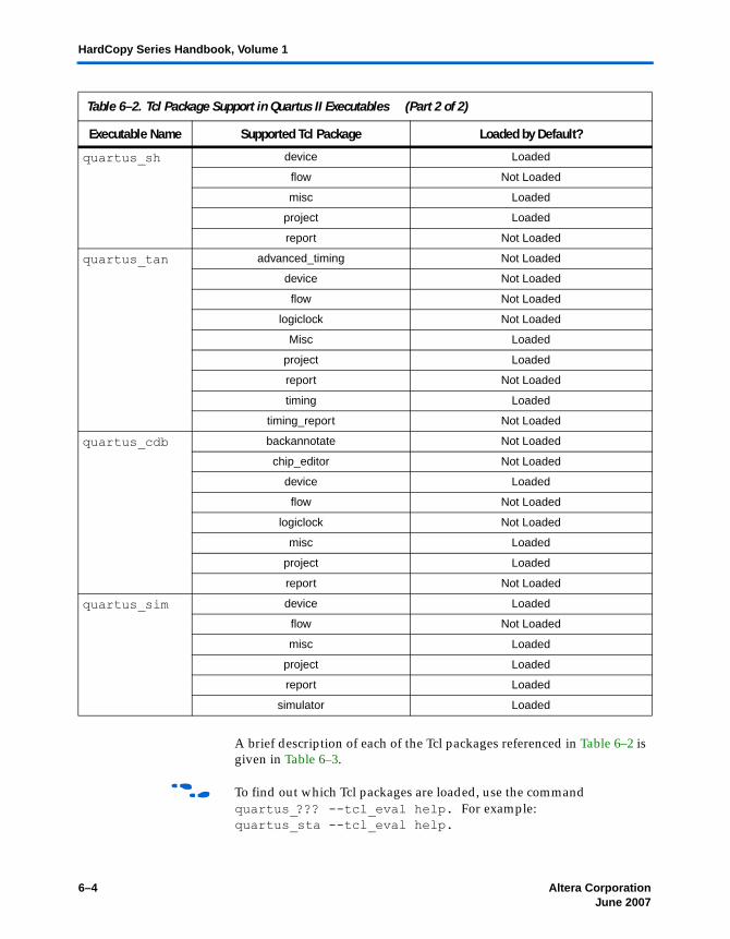
6–4 Altera Corporation June 2007
HardCopy Series Handbook, Volume 1
A brief description of each of the Tcl packages referenced in Table 6–2 is given in Table 6–3.
f To find out which Tcl packages are loaded, use the command quartus_??? --tcl_eval help. For example:quartus_sta --tcl_eval help.
quartus_sh device Loaded
flow Not Loaded
misc Loaded
project Loaded
report Not Loaded
quartus_tan advanced_timing Not Loaded
device Not Loaded
flow Not Loaded
logiclock Not Loaded
Misc Loaded
project Loaded
report Not Loaded
timing Loaded
timing_report Not Loaded
quartus_cdb backannotate Not Loaded
chip_editor Not Loaded
device Loaded
flow Not Loaded
logiclock Not Loaded
misc Loaded
project Loaded
report Not Loaded
quartus_sim device Loaded
flow Not Loaded
misc Loaded
project Loaded
report Loaded
simulator Loaded
Table 6–2. Tcl Package Support in Quartus II Executables (Part 2 of 2)
Executable Name Supported Tcl Package Loaded by Default?

Altera Corporation 6–5June 2007
Tcl Support in the Quartus II Software
The Quartus II command-line executables and Tcl shells are supported on all Quartus II operating systems, including Microsoft Windows, Linux, and Unix platforms.
f For more information on Quartus II Tcl packages and their available Tcl procedures, refer to the Tcl Packages and Commands chapter in the Quartus II Scripting Reference Manual.
Command-Line Processing
In addition to the interactive Tcl shell, the Quartus II command-line executables support command-line switches for executing Tcl scripts and commands. When used with these switches, a command-line executable quits when complete. The command-line executables also provide switches for performing specific Quartus II operations. For example, the following c-shell script takes as its argument the top-level design file and entity name and runs it through the entire HardCopy II design flow.
!#/bin/cshquartus_sh --flow compile %1quartus_cdb %1 --create_companion=%1_hciiquartus_sh --flow compile %1 -c %1_hciiquartus_cdb --compare=%1_hcii %1 -c %1
Table 6–3. Quartus II Tcl Package Descriptions
Tcl Package Description
advanced_timing Traverse the timing netlist and get information about timing modes.
backannotate Back annotate assignments.
chip_editor Identify and modify resource usage and routing with the Chip Editor.
database_manager Manage version-comparable database files.
device Get device and family information from the device database.
flow Compile a project, run command-line executables and other common flows.
logiclock Create and manage LogicLock regions.
misc Perform miscellaneous tasks.
project Create and manage projects and revisions and make any project assignments including timing assignments.
report Get information from report tables and create custom reports.
simulator Configure and perform simulations.
stp Operate the SignalTap® II Analyzer.
timing Annotate timing netlist with delay information, compute and report timing paths.
timing_report List timing paths.

6–6 Altera Corporation June 2007
HardCopy Series Handbook, Volume 1
This example shows what is, perhaps, the simplest way to execute the HardCopy II design flow. If you have developed and applied the design I/O, location and timing constraints for the project, these constraints are included during script execution.
f For more information on the Quartus II executables and command-line options, refer to the Command-Line Executables chapter in the Quartus II Scripting Reference Manual and the Command-Line Scripting section in volume 2 of the Quartus II Handbook.
The HardCopy II Design Flow
The Quartus II software supports both HardCopy II first and Stratix II first design flows. The Stratix II first flow involves the following:
■ Compiling for the Stratix II FPGA prototype■ Verifying the Stratix II FPGA prototype■ Migrating the prototype design to a HardCopy II design■ Compiling the HardCopy II design■ Transferring your HardCopy II files to the Altera® Design Center
The Hardcopy II first flow is similar, but starts with compiling the HardCopy II target device. Once the HardCopy II compile completes successfully, the design is migrated to the Stratix II target.
The HardCopy II design flow in the Quartus II software is shown in Figure 6–1. To begin a design, create a new project and revision for the Stratix II FPGA prototype. Apply Quartus II settings together with I/O assignments and timing constraints. Compile the Stratix II prototype revision (synthesis, place and route, and assembly) to produce a complete layout, with timing closure and free from errors. You can now perform any additional functional and timing verification necessary and then implement and verify the prototype in hardware.
Once the FPGA prototype is verified, you can compile the HardCopy II design. Begin by creating a HardCopy II companion revision for the FPGA prototype:
1. Create a HardCopy II companion revision for the FPGA prototype. All design settings and constraints are automatically migrated to the new companion revision.
2. Compile the HardCopy II revision. As the compile runs, the Design Assistant checks for errors. When the compile completes, you should correct errors and resolve failures that appear in the Quartus II reports.

Altera Corporation 6–7June 2007
The HardCopy II Design Flow
3. Run the HardCopy II Companion Revision Comparison tool to compare the HardCopy II design against the FPGA prototype. The comparison tool checks for structural equivalency and consistency between the two revisions.
4. If there are no mismatches, you can prepare the HardCopy II design files for transfer to the Altera Design Center.
1 In addition to design verification in the Quartus II software, the flow can generate files required to perform Static Timing Analysis (STA) in Synopsys’ Primetime.
Figure 6–1. The HardCopy II Design Flow
Create a New Project
Make Global Assignments
Make Location Assignments
Make Timing Assignments
Prot
otyp
e St
ratix
II D
esig
n
Hard
Copy
II D
esig
n
Source .v, .vhd, .tdf.edf, .bdf Design Files
Verify the Stratix II Prototype
Compile Stratix II PrototypeCompilation Report Files
Timing ConstraintTcl Files
Compile HardCopy II Design
Create HardCopy II CompanionRevision
Verify HardCopy II Design
Hand-Off to the Altera DesignCenter
HardCopy II Archive
Compare DesignReport File
Signal-Pin AssignmentTcl Files
CompilationReport Files

6–8 Altera Corporation June 2007
HardCopy Series Handbook, Volume 1
The design flow of Figure 6–1 begins with a Stratix II FPGA prototype design and migrates this design to a HardCopy II device target, or begins with a HardCopy II target and migrates this design to a Stratix II target for FPGA prototyping. The design flow for both cases is shown in Figure 6–1.
f For more information on the HardCopy II design flow and alternative methods to complete HardCopy II designs using the Quartus II GUI, refer to the Quartus II Support for HardCopy II Devices chapter in the Quartus II Handbook or the HardCopy II Design Considerations chapter in volume 1 of the HardCopy Series Handbook.
The following sections describe each step of the flow shown in Figure 6–1 and explains how each step is completed using the interactive Tcl shell.
Creating a New Project
Both FPGA and HardCopy design in the Quartus II software revolve around the use of projects. You must create a project before you begin working with a new design. A project includes source design files (RTL and schematics), Quartus II tool settings, and a set of pin locations and timing constraints. Although a project can contain many different revisions for a design, each revision can have a unique set of design constraints, target device settings, and Quartus II software settings. You must explicitly open a project before you can perform other operations on the project. You must close the current project to switch to a different project or revision.
This section details the different operations relating to project management using Tcl commands.
Creating a Stratix II Prototype Project
To create a new Stratix II prototype project, use the project_new Tcl command. The syntax for this command is:
tcl> project_new [-family <family>] [-overwrite] \[-part <part>] [-revision <revision_name>] \<project_name>
The only required argument for this command is the project name, <project name>, although the target device family, part code, and revision name can be specified at this time also. By default, the revision name is the same as the project name. The device family and part code can be set later using the set_global_assignment command. For example, to create

Altera Corporation 6–9June 2007
Creating a New Project
a project called demo_design with the default revision name of demo_design and an unspecified target device family or part, the following Tcl command is executed:
tcl> project_new demo_design
Creating a new project creates a quartus settings file (QSF) and a Quartus II Project file (QPF) in the current directory. In addition, a db subdirectory is created that is used to store Quartus II database files. In the case of the demo_design project example, the following files are created in the project directory:
demo_design.qpfdemo_design.qsfdb/
demo_design.db_info
Opening a Project
The project created automatically opens when you use the project_new command. In future Quartus II sessions, or if you close the project, you must open the project with the Tcl command: project_open. The syntax for the project_open command is:
tcl> project_open [-current_revision] \[-revision <revision_name>] <project_name>
For example, to open the default revision of project demo_design, execute the following Tcl command:
tcl> project_open demo_design
1 It is a good practice to have consistent names for the Stratix II and HardCopy II revisions of your project. This makes it easy to identify which revision is which. For example, naming your revisions projectname_fpga and projectname_hcii would help you easily identify which revision is the Stratix II revision, and which is the HardCopy II revision.
Closing a Project
Before ending a Quartus II project session, it is good practice to close the Quartus II project using the project_close command. This ensures that any changes you have made to your project are written to the Quartus II QSF file. The syntax for the project_close command is:
tcl> project_close [-dont_export_assignments]

6–10 Altera Corporation June 2007
HardCopy Series Handbook, Volume 1
New Project Example Script
The following script shows the use of Tcl commands for opening and closing a project called demo_design with the revision name, demo_design_fpga. If the project does not already exist, it is created. This script makes use of the project_exists and project_open Tcl commands.
## Example Tcl Script for opening and closing a project
## Open Project demo_design. If the Project does not Already ## Exist, Create itif [is_project_open] project_closeif [project_exists demo_design] { project_open demo_design -revision demo_design_fpga} else { project_new demo_design -revision demo_design_fpga}
## Include Other Tcl Commands Here …
## Close project demo_design and write any changes to settings to ## demo_design.qsfproject_close
## End of script
f For more information on these and other useful project-related commands, refer to the Project section in the Tcl Packages and Commands chapter in the Quartus II Scripting Reference Manual.
Altera Corporation 6–11June 2007
Making Global Assignments
Making Global Assignments
Initializing a HardCopy II Design
For a HardCopy II design, the following key operations are required after a Quartus II project is created:
■ Specify design source files (Verilog, VHDL, AHDL, EDIF, and BDF files)
■ Specify the Stratix II prototype target family and device name■ Specify the HardCopy II companion revision and migration device■ Enable the Design Assistant■ Make recommended HardCopy II specific Quartus II tool settings
In addition to these, other project settings affecting downstream tools, such as synthesis and place-and-route, can be made at this time.
The operations listed above are performed using the set_global_assignment command. The syntax for this command is:
tcl> set_global_assignment [-comment<comment>] \[-disable] [-entity <entity_name>] -name <name> \[-remove] [-section_id <section_id>] <value>
The most important parameters for the set_global_assignment command are <name> and <value>. The <name> argument specifies the Quartus II global variable to be set and <value> is the new value assigned to that variable.
One of the steps in initializing a HardCopy II design is to turn on the Design Assistant. When run in the GUI, the Design Assistant provides a visual checklist for running both the Stratix II and HardCopy II phases of the design. For first-time users, this can provide a powerful guide for successfully completing your HardCopy II project.

6–12 Altera Corporation June 2007
HardCopy Series Handbook, Volume 1
The key global variables for a HardCopy II project are listed in Table 6–4.
Table 6–4. Key HardCopy II Design Settings
Global Variable Name <name> Value Description <value>
VERILOG_FILE Verilog file name.
VHDL_FILE VHDL file name.
AHDL_FILE Altera HDL file name.
EDIF_FILE EDIF file name.
BDF_FILE Altera schematic file name.
FAMILY Device family name, for example, Stratix II.
DEVICE Prototype FPGA target device name.
TOP_LEVEL_ENTITY Top-level design entity or module name.
DEVICE_TECHNOLOGY_MIGRATION_LIST HardCopy II target device name.
COMPANION_REVISION HardCopy II design revision name.
ENABLE_DRC_SETTINGS Turn on the Design Assistant.
USE_TIMEQUEST_TIMING_ANALYZER Set TimeQuest as the default timing analyzer <ON>.
SDC_FILE File of TimeQuest constraints <constraint_file.sdc>.
You only need the following settings when using Classic Timing Analyzer. Using Classic Timing Analyzer is not recommended.
REPORT_IO_PATHS_SEPARATELY Creates a separate report panel for input and output min and max timing results.
FLOW_ENABLE_TIMING_CONSTRAINT_CHECK Timing constraints are checked for completeness (all clock domains constraints and minimum and maximum constraints are set for all I/O paths).
DO_COMBINED_ANALYSIS Timing analysis are run for fast and slow operating conditions and for best and worst-case timing analysis, respectively.
IGNORE_CLOCK_SETTINGS This must be turned off.
ENABLE_RECOVERY_REMOVAL_ANALYSIS Verify recovery and removal times on asynchronous control and reset signals.
ENABLE_CLOCK_LATENCY Clock latency is included in timing analysis to asses clock-insertion timing and clock skew.

Altera Corporation 6–13June 2007
Making Global Assignments
The DEVICE and DEVICE_TECHNOLOGY_MIGRATION_LIST variables are the parts used for the Stratix II prototype design and the HardCopy II design. The selected Stratix II prototype device must be compatible with the selected HardCopy II device to make migration possible. Valid pairings for these devices are listed in Table 6–5.
For the DEVICE_TECHNOLOGY_MIGRATION_LIST variable, the HardCopy II part names listed in Table 6–5 are used. For the DEVICE variables, the Stratix II part names include the speed grade for the part. The speed grade is a two character code indicating industrial (I) or commercial (C) and the speed indicator (number 3, 4, or 5). For example, a -4 commercial part is denoted using the two character speed grade C4. The two-character speed grade is appended to the Stratix II part name to form the value string for the DEVICE variable.
Table 6–5. Stratix II Prototype Options for HardCopy II (Part 1 of 2)
HardCopy II Part Stratix II Prototype Part
HC210F484CHC210W484C
EP2S30F484C3EP2S30F484C4EP2S30F484C5EP2S30F484I4
EP2S60F484C3EP2S60F484C4EP2S60F484C5EP2S60F484I4
EP2S90H484C4EP2S90H484C5
HC220F672C EP2S60F672C3EP2S60F672C4EP2S60F672C5EP2S60F672I4
HC220F780C EP2S90F780C4EP2S90F780C5
EP2S130F780C4EP2S130F780C5

6–14 Altera Corporation June 2007
HardCopy Series Handbook, Volume 1
The following two Tcl commands demonstrate setting the DEVICE and DEVICE_TECHNOLOGY_MIGRATION_LIST variables.
tcl> set_global_assignment -name DEVICE EP2S90F1020C4tcl> set_global_assignment -name \
DEVICE_TECHNOLOGY_MIGRATION_LIST HC230F1020C
HC230F1020C EP2S90F1020C3EP2S90F1020C4EP2S90F1020C5EP2S90F1020I4
EP2S130F1020C3EP2S130F1020C4EP2S130F1020C5EP2S130F1020I4
EP2S180F1020C3EP2S180F1020C4EP2S180F1020C5EP2S180F1020I4
HC2401020C EP2S180F1020C3EP2S180F1020C4EP2S180F1020C5EP2S180F1020I4
HC240F1508C EP2S180F1508C3EP2S180F1508C4EP2S180F1508C5EP2S180F1508I4
Table 6–5. Stratix II Prototype Options for HardCopy II (Part 2 of 2)
HardCopy II Part Stratix II Prototype Part
Altera Corporation 6–15June 2007
Making Global Assignments
The Design Assistant
You should turn on the Design Assistant at the beginning of the design process by turning on the ENABLE_DRC_SETTINGS global variable.
tcl> set_global_assignment \-name ENABLE_DRC_SETTINGS ON
The Design Assistant runs concurrently with every step of both the prototype Stratix II and HardCopy II design flows. When the Design Assistant is turned on, the Quartus II software checks to ensure that the project fully complies with all HardCopy II design rules and requirements.
f For more information on the Design Assistant, refer to the Design Guidelines for HardCopy II Devices chapter in volume 1 of the HardCopy Series Handbook and the Quartus Support for HardCopy II Devices chapter in the Quartus II Handbook.

6–16 Altera Corporation June 2007
HardCopy Series Handbook, Volume 1
Example Tcl Script for Making Global Assignments
The example Tcl script below illustrates the application of global constraints for a HardCopy II project.
## Example Global Assignments Script for a HardCopy II Design## This Script Applies Settings for a EP2S90 Stratix II ## prototype FPGA target and a HC230 HardCopy II target
## Source Design File Settings## ===========================set_global_assignment -name VERILOG_FILE demo_design.vset_global_assignment -name VERILOG_FILE example_ram.v
## Stratix II Prototype FPGA Target Settings## =========================================set_global_assignment -name FAMILY "Stratix II"set_global_assignment -name DEVICE EP2S90F1020C4set_global_assignment -name TOP_LEVEL_ENTITY demo_design
## HardCopy II Companion Revision and Target Settings## ==================================================set_global_assignment -name COMPANION_REVISION_NAME \
demo_design_hardcopyiiset_global_assignment -name DEVICE_TECHNOLOGY_MIGRATION_LIST HC230F1020
## Design Assistant Assignments and Settings Required for HardCopy II ##==============================================================set_global_assignment -name ENABLE_DRC_SETTINGS ONset_global_assignment -name ERROR_CHECK_FREQUENCY_DIVISOR 1set_global_assignment -name REPORT_IO_PATHS_SEPARATELY ON
## The following assignments are Classic Timing Analyzer only ## and are not used by TimeQuest.##===========================================================set_global_assignment -name FLOW_ENABLE_TIMING_CONSTRAINT_CHECK ONset_global_assignment -name DO_COMBINED_ANALYSIS ONset_global_assignment -name IGNORE_CLOCK_SETTINGS OFF
set_global_assignment -name ENABLE_RECOVERY_REMOVAL_ANALYSIS ONset_global_assignment -name ENABLE_CLOCK_LATENCY ON
## End of Script

Altera Corporation 6–17June 2007
Making Global Assignments
Making I/O Assignments
Because of the complex rules governing the use of programmable I/O cells and their availability for specific pins and packages, Altera highly recommends that I/O assignments are completed using the Pin Planning tool and the Assignment Editor in the Quartus II GUI. These tools ensure that all of the rules regarding each pin and I/O cell are applied correctly. The Quartus II GUI can export a Tcl script containing all I/O assignments and specifications. I/O assignments are described here for information only.
f For more information on I/O location and type assignments using the Quartus II Assignment Editor and Pin Planner tools, refer to the Assignment Editor chapter in volume 2 of the Quartus II Handbook.
In this section, I/O specification is considered in two parts:
■ Pin assignments■ I/O type assignments
Pin Assignments
Design I/O signals are assigned to package balls using the set_location_assignment command. The syntax for this command is given below:
tcl> set_location_assignment [-comment <comment>] \[-disable] [-remove] -to <destination> <value>
Here, <destination> is the package ball name and <value> is the design I/O signal name. For BGA and FBGA packages, the ball name follows the form PIN_<coordinate>. For example, to assign design I/O signal data_out[15] to package ball AL17:
tcl> set_location_assignment -to PIN_AL17 data_out[15]
Setting I/O Type and Parameters
For I/O type and parameter specification, the set_instance_assignment command is used. The syntax for this command is:
tcl> set_instance_assignment [-comment <comment>] \[-disable] [-entity <entity_name>] \[-from <source>] -name <name> [-remove] \[-section_id <section_id>] \[-to <destination>] <value>

6–18 Altera Corporation June 2007
HardCopy Series Handbook, Volume 1
The assignment name, <name>, should be set to IO_STANDARD to indicate that an I/O specification is being applied. The related I/O signal is specified as -to <destination>. The destination argument is a string providing details on the I/O type, such as levels and standards. Table 6–6 lists the strings corresponding to the I/O standards supported in HardCopy II devices.
Table 6–6. Tcl I/O Standard Strings
I/O Type or <name> Description
LVTTL LVTTL I/O
LVCMOS LVCMOS I/O
“3.3-V PCI” 3.3-V PCI I/O
“3.3-V PCI-X” 3.3-V PCI X I/O
“1.5 V“ 1.5-V I/O
“1.8 V” 1.8-V I/O
“2.5 V” 2.5-V I/O
“1.5-V HSTL CLASS I” QDRII SRAM 1.5-V I/O
“1.5-V HSTL CLASS II” QDRII SRAM 1.5-V I/O
“1.8-V HSTL CLASS I” QDRII SRAM/RLDRAM II 1.8-V I/O
“1.8-V HSTL CLASS II” QDRII SRAM/RLDRAM II 1.8-V I/O
“DIFFERENTIAL 1.5-V HSTL CLASS I” Memory clock interface
“DIFFERENTIAL 1.5-V HSTL CLASS II” Memory clock interface
“DIFFERENTIAL 1.8-V HSTL CLASS I” Memory clock interface
“DIFFERENTIAL 1.8-V HSTL CLASS II” Memory clock interface
“DIFFERENTIAL 1.8-V SSTL CLASS I” DDR2 SDRAM
“DIFFERENTIAL 1.8-V SSTL CLASS II” DDR2 SDRAM
“DIFFERENTIAL SSTL-2” DDR SDRAM
“DIFFERENTIAL 2.5-V SSTL CLASS II” DDR SDRAM
“SSTL-18 CLASS I” DDR2 SDRAM
“SSTL-18 CLASS II” DDR2 SDRAM
“SSTL-2 CLASS I” DDR SDRAM
“SSTL-2 CLASS II” DDR SDRAM
LVDS 2.5-V differential signaling
HYPERTRANSPORT 2.5-V differential signaling
LVPCL Differential

Altera Corporation 6–19June 2007
Making Global Assignments
You can specify a number of other I/O parameters by using the set_instance_assignment command. Some of the more common parameters are listed in Table 6–7.
f For more information on I/O availability in HardCopy II devices, refer to the I/O Structures and Features section in volume 1 of the HardCopy Series Handbook.
Table 6–7. Tcl Common I/O Parameter Settings
<name> setting <value> setting Description
weak_pull_up_resistor on Implement a weak pull-up resistor on the pin.
output_pin_load integer Capacitive load for an output or bidirectional pin. Units of pF.
fast_output_register on Implements a fast output register in the I/O cell or adjacent LAB.
fast_output_enable_register on Implement a fast output enable register in the I/O cell or/and adjacent LAB.
fast_input_register on Implements a fast input register in the I/O cell or adjacent LAB.
current_strength_new 2 mA, 4 mA, 8 mA, 10 mA,12 mA, 16 mA, 18 mA,
20 mA, 24 mAminimum_current or maximum_current
Drive strength for an output or bidi pin.
stratixii_termination differential“series 25 ohms with calibration”
“series 25 ohms without calibration”“series 50 ohms with calibration”
“series 50 ohms without calibration”
On-chip termination (or impedance matching) for an I/O pin.

6–20 Altera Corporation June 2007
HardCopy Series Handbook, Volume 1
I/O Assignment Example Script
The following Tcl script example specifies several different I/O constraints.
## Signal-Ball Assignmentsset_location_assignment PIN_AH5 -to addr_out[0]set_location_assignment PIN_AH6 -to addr_out[1]set_location_assignment PIN_AJ5 -to data_in[0]set_location_assignment PIN_AJ6 -to data_in[1]set_location_assignment PIN_AJ32 -to resetnset_location_assignment PIN_AM17 -to ref_clk
# I/O Type and Parameter Assignmentsset_instance_assignment -name IO_STANDARD "1.5-V HSTL CLASS II" -to addr_out[0]set_instance_assignment -name IO_STANDARD "1.5-V HSTL CLASS II" -to addr_out[1]set_instance_assignment -name IO_STANDARD "1.5-V HSTL CLASS II" -to data_in[0]set_instance_assignment -name IO_STANDARD "1.5-V HSTL CLASS II" -to data_in[1]set_instance_assignment -name IO_STANDARD LVDS -to resetnset_instance_assignment -name IO_STANDARD LVCMOS -to ref_clk
set_instance_assignment -name fast_input_register on -to data_in[0]set_instance_assignment -name fast_input_register on -to data_in[1]set_instance_assignment -name fast_output_register on -to addr_out[0]set_instance_assignment -name fast_output_register on -to addr_out[1]
set_instance_assignment -name output_pin_load 10 -to addr_out[0]set_instance_assignment -name output_pin_load 10 -to addr_out[1]set_instance_assignment -name current_strength_new 16mA -to addr_out[0]set_instance_assignment -name stratixii_termination “series 25 ohms without calibration”\-to data_in[1]
Assigning Timing Constraints
Planning Design Timing Constraints
Timing constraints ensure that a design compiled in the Quartus II software meets specific timing requirements. When you target an FPGA, you may decide not to apply a complete set of timing constraints, choosing instead to fix any timing problems in your prototype system if and when they arise. HardCopy devices, however, cannot be modified using reconfiguration to fix timing problems, so it is critically important that a design is fully constrained. Designs not fully constrained would result in significantly different timing characteristics between the prototype Stratix II FPGA and the HardCopy II device. By fully constraining a design, Altera can guarantee that both the Stratix II FPGA and the HardCopy II device fully complies with your timing specifications.

Altera Corporation 6–21June 2007
Assigning Timing Constraints
The minimum set of timing constraints for a HardCopy II design are:
■ Clock settings (FMAX) for each and every clock domain■ Minimum and maximum delays for all I/O paths, including
asynchronous reset and control I/O signals
In addition, it is good design practice to develop timing constraints to cover:
■ Specific cross-clock domain timing requirements■ False paths■ Multicycle paths
In TimeQuest, timing constraints are written in TimeQuest SDC format and are read from an SDC file. An example file is demo_design.sdc. See “Using TimeQuest” on page 6–30.
In the Classic Timing Analyzer, timing constraints are applied using dedicated Tcl commands and by assigning timing-specific attributes using the set_instance_assignment command.
This section provides an overview of timing constraint development using Tcl commands.
f For more information on timing constraints, refer to the Timing Analysis section in volume 3 of the Quartus II Handbook.
Specifying System Clocks
The most basic constraints that should be applied describe the clock for each clock domain. Parameters usually specified for each clock are:
■ Clock period■ Latency (LATE_CLOCK_LATENCY/EARLY_CLOCK_LATENCY
assignments)■ Uncertainty (set_clock_uncertainty command)
Clock uncertainty specified with the set_clock_uncertainty command models any uncertainty in the clock period, including jitter, and is often used to introduce some margin into the target clock frequency. The following example constraints illustrate clock definition for a design with two clock domains, clk_a and clk_b. In this case, both clocks run at 100 MHz, but with different clock latency and skew.
## Example TimeQuest SDC Constraints Defining Clocks clk_a and clk_bcreate_clock -period 10.0 -name clk_a [get_ports clk_a]set_clock_latency -source -late 3.0 clk_aset_clock_latency -source -early 2.0 clk_a

6–22 Altera Corporation June 2007
HardCopy Series Handbook, Volume 1
set_clock_uncertainty -to clk_a 0.25
create_clock -period 10.0 -name clk_b [get_ports clk_b]set_clock_latency -source -late 4.0 clk_bset_clock_latency -source -early 3.0 clk_bset_clock_uncertainty -to clk_b 0.25
Input/Output Timing
System clock parameters define the setup and hold timing for register to register paths within each clock domain. I/O timing parameters are used to describe I/O to register, and register to I/O timing.
The set_input_delay constraint is used to specify the delay from a source external to the chip to an input pin, relative to a defined clock. The syntax for this command is given below.
set_input_delay \-clock <clock name> \[-clock_fall] \[-rise | -fall] \[-max | -min] \[-add_delay] \[-reference_pin <pin or port>] \<delay value> \<port pin list>
The <clock name> argument specifies the reference clock for the delay. The <port pin list> argument is the top-level input signal for the design, and <delay value> is the external delay. The external delay is measured from the positive (rising) edge of <clock> unless the -clock_fall argument is specified. The -min and -max arguments are used to specify whether <delay value> is the minimum or maximum external delay, respectively.
The set_output_delay constraint is similar to the set_input_delay constraint except that it specifies the delay from an output pin to its external destination relative to a clock.
set_output_delay \-clock <clock name> \[-clock_fall] \[-rise | -fall] \[-max | -min] \[-add_delay] \[-reference_pin <pin or port>] \<delay value> \<port pin list>

Altera Corporation 6–23June 2007
Assigning Timing Constraints
As an example, the following Tcl script specifies input and output min and max delays for two I/O signals. Input data_in[0] has minimum and maximum external delays of 3 ns and 7 ns, respectively. Output data_out[0] has minimum and maximum external delays of 4 ns and 8 ns, respectively. The external input delays for data_in[0] are relative to the positive edge of clock ref_clk and the external output delays for data_out[0] are relative to the negative edge of clock ref_clk.
# Tcl Script Setting I/O Timing Using set_input_delay and set_output_delayset_input_delay -clock ref_clk -max 7.0 [get_ports data_in[0]]set_input_delay -clock ref_clk -min 3.0 [get_ports data_in[0]]set_output_delay -clock ref_clk -max 8.0 [get_ports data_out[0]]set_output_delay -clock ref_clk -min 4.0 [get_ports data_out[0]]
Creating Timing Exceptions
Timing exceptions are used to correct timing constraints not covered by clock settings and I/O timing settings. The most common of these are multicycle paths and false paths.
In TimeQuest, multicycle paths are described using the set_multicycle_path constraint. The syntax for this constraint is:
set_multicycle_path [-setup][-hold][-start]
In Classic Timing Analyzer, multicycle paths are described using the set_multicycle_assignment command. The syntax for this command is:
tcl> set_multicycle_assignment [-comment <comment>] \[-disable] [-end] [-from <from_list>] \[-hold] [-remove] [-setup] [-start] \[-to <to_list>] <path_multiplier>
In either timing analyzer, multicycle assignments are made with the -setup argument, to specify the maximum number of cycles, or with the -hold argument, to specify the minimum number of cycles for a path.
False paths describe paths that should not be included in timing optimization or analysis operations. In the Quartus II software, there are a number of ways to describe false paths. By default, in Classic Timing Analyzer, feedback from the output to input side of bidirectional I/O, read-while-write paths through memories, and cross-clock domain paths are not timed during optimization or timing analysis. By default, in Time Quest, cross-clock domain paths are timed.

6–24 Altera Corporation June 2007
HardCopy Series Handbook, Volume 1
f To change these default settings, refer to the Timing Settings section in the Quartus II Support of HardCopy Series Devices chapter in volume 1 of the Quartus II Handbook.
In TimeQuest, the constraint set_false_path is used to describe paths that should not be included in timing optimization or analysis. The syntax for this constraint is:
tcl> set_false_path \[-from <from list>] \[-to <to list>] \[-thru <thru list>]
In Classic Timing Analyzer, the most common command for controlling false paths is the set_timing_cut_assignment command. The syntax for this command is:
tcl> set_timing_cut_assignment \[-comment <comment>] \[-disable] \[-from <from_pin_list>] \[-remove] \[-to <to_pin_list>]
All paths between nodes in the <from_pin_list> to nodes in the <to_pin_list> are excluded from timing optimization and analysis operations.
Example of TimeQuest SDC Constraints# Timing Assignments# ==================create_clock –period 10.0ns -name ref_clk ref_clk
set_clock_latency -late 3 ref_clkset_clock_latency -early 2 ref_clkset_clock_uncertainty –hold –to ref_clk 0.250nsset_clock_uncertainty –setup –to ref_clk 0.250ns
# Input delay of 6ns (max) & 2ns (min) for bus data_in[1:0]set_input_delay –clock ref_clk –max 6 data_inset_input_delay –clock ref_clk –min 2 data_in
# Output delay of 6ns (max) & 2ns (min) for bus data_out[1:0]set_output_delay –clock ref_clk –max 6 data_outset_output_delay –clock ref_clk –min 2 data_out
# Don’t care about timing on the resetn net. Set as false pathset_false_path -from resetn

Altera Corporation 6–25June 2007
Compiling the Stratix II Prototype Design
Example of Classic Timing Analyzer Tcl Script # Timing Assignments# ==================create_base_clock –fmax 100 MHz –target ref_clk ref_clk
set_instance_assignment -name LATE_CLOCK_LATENCY 3ns -to ref_clkset_instance_assignment -name EARLY_CLOCK_LATENCY 2ns -to ref_clkset_clock_uncertainty –hold –to ref_clk 0.250nsset_clock_uncertainty –setup –to ref_clk 0.250ns
# Input delay of 6ns (max) & 2ns (min) for bus data_in[1:0]set_input_delay –clk_ref ref_clk –max –to data_in 6.0nsset_input_delay –clk_ref ref_clk –min –to data_in 2.0ns
# Output delay of 6ns (max) & 2ns (min) for bus data_out[1:0]set_output_delay –clk_ref ref_clk –max –to data_out 6.0nsset_output_delay –clk_ref ref_clk –min –to data_out 2.0ns
# Don’t care about timing on the resetn net. Set as false pathset_timing_cut_assignment -from resetn
This section has provided an overview of Tcl commands for applying timing constraints.
f For more information on the application of timing constraints using Tcl commands, refer to the Tcl Packages and Commands chapter in the Quartus II Scripting Reference Manual.
Compiling the Stratix II Prototype Design
Once all global assignments, resource assignments, and timing assignments have been specified, the next step in the design process is to compile the Stratix II FPGA prototype design. The execute_flow command is provided for this purpose and supports various arguments affecting the compilation process. The syntax for this command is:
tcl> execute_flow \[-analysis_and_elaboration] \[-attempt_similar_placement] \[-check_ios] \[-check_netlist] \[-compile] \[-compile_and_simulate] \[-early_timing_estimate] \[-eco] [-export_database] \[-fast_model] \[-generate_functional_sim_netlist] \[-import_database]

6–26 Altera Corporation June 2007
HardCopy Series Handbook, Volume 1
The switches relevant to prototype Stratix II and HardCopy II design are listed in Table 6–8.
1 It is important to note that the HardCopy switches for the execute_flow command are for HardCopy Stratix designs, not HardCopy II designs.
The simplest way to run the execute_flow command is to use the -compile switch.
tcl> execute_flow -compile
Running the execute_flow command in this way executes the four stages of the Quartus II compilation flow with default settings for each stage:
■ Analysis and Synthesis■ Fitter■ Timing Analysis■ Assembler
Table 6–8. execute_flow Tcl Command Switches
Switch Description
analysis_and_elaboration Perform synthesis and mapping to the target Altera technology
attempt_similar_placement Runs Attempt Similar Placement
check_ios Verify I/O assignments
check_netlist Perform syntax checks on the netlist
compile Execute the Quartus II compilation flow
compile_and_simulate As for compile, but also run simulation
early_timing_estimate Runs the early timing estimator
eco Executes a Fitter ECO compilation
export_database Exports a Version-Compatible Database
fast_model Runs Timing Analysis (fast mode analysis)
generate_functional_sim_netlist Generate a Simulation Netlist
import_database Imports a Version-Compatible Database

Altera Corporation 6–27June 2007
Compiling the HardCopy II Design
The Design Assistant and Timing constraint checks are run if they are enabled in the Quartus II Settings file.
You should check I/O assignments to avoid problems in downstream compile operations. To do this, the execute_flow compilation is broken into three steps:
1. tcl> execute_flow -analysis_and_elaboration
2. tcl> execute_flow -check_ios
3. tcl> execute_flow -compile
It should be noted that, in the interests of clarity and brevity, the Tcl fragments given here do not incorporate any error checking. However, it is good practice to include code in your Tcl scripts that checks for success as your design proceeds. In the case of the execute_flow procedure, the return value can be used with the Tcl catch command to handle success or failure. The example below shows one option for doing this.
# Determine if compilation was successful and # print out a personalized message.if {[catch {execute_flow -compile} result]} {
puts "\nResult: $result\n"puts
"ERROR: Compilation failed. See report files.\n"} else {
puts "\nINFO: Compilation was successful.\n"}
f For more information on the execute_flow command, refer to the command description in the Tcl Packages and Commands chapter in the Quartus II Scripting Reference Manual.
Compiling the HardCopy II Design
Once the Stratix II FPGA prototype design is compiled and verified, you can compile the HardCopy II revision of the design. This is a two-step process:
1. Create the HardCopy II companion revision.
2. Compile the HardCopy II companion revision.
To create the HardCopy II version of the design, run the execute_hardcopyii Tcl command with the -create_companion option:
tcl> execute_hardcopyii -create_companion demo_design_hcii

6–28 Altera Corporation June 2007
HardCopy Series Handbook, Volume 1
This command initializes the database for the HardCopy II revision and creates a new QSF file (in this example, demo_design_hcii.qsf), ensuring that all constraints for the Stratix II FPGA revision are ported over.
Next, the current working revision for the Quartus II project is changed to the HardCopy II revision and the design is compiled for the HardCopy II device target:
tcl> set_current_revision demo_design_hciitcl> execute_flow -compile
As with the prototype Stratix II revision, report files are generated in the project directory for each of the tools that are executed.
Understanding Report Files
The execute_flow command generates a number of report files in the project directory. These files summarize messages displayed on the console during compilation and provide additional information about the design. The name of each report file follows the format <revision><tool short name>.summary and <revision><tool short name>.rpt, where <revision> is the revision name of the current design. The .summary file contains a brief summary of messages and results from the tool while the .rpt file contains more detailed messages and information. For a HardCopy II project, two sets of report files are generated: one for the Stratix II prototype FPGA revision and one for the HardCopy II revision. Table 6–9 describes the different report files.
1 The Tcl report package provides a powerful collection of procedures for customizing and managing report files related to the Quartus II fitter and timing analysis engines.
f For more information on customizing and managing report files, refer to the Tcl Packages and Commands report section of the Quartus II Tcl Reference Manual.
Table 6–9. Stratix II Compile Report File Descriptions (Part 1 of 2)
Switch Tool Description
<revision>.map.rpt Analysis & Synthesis Synthesis settings, source files, messages, and resource usage.
<revision>.map.eqn Analysis & Synthesis Implementation equations and device resource instantiations.
<revision>.fit.rpt Fitter Fitter settings, layout optimizations, resources, pin-out, and messages.
<revision>.fit.eqn Fitter Implemented equations and device resource instantiations after fitting.
<revision>.drc.rpt Design Assistant Design rule settings, violations, and messages.

Altera Corporation 6–29June 2007
Comparing FPGA and HardCopy Revisions
Comparing FPGA and HardCopy Revisions
Before submitting the HardCopy II project to the Altera Design Center, it should be checked against the Stratix II prototype FPGA revision. To do this, run the execute_hardcopyii Tcl command with the -compare option from the quartus_sh shell:
tcl> execute_hardcopyii -compare
Running this command generates a report file and summary file in the project directory. These files are called <revision_name>.rec.rpt and <revision_name>.rec.summary. The command checks to verify that the following items conform to HardCopy II design rules and are consistent between the HardCopy II and Stratix II revisions:
■ Source design files and device netlist files■ User clock assignments■ Timing constraints (assignments)■ I/O location and type assignments■ PLL parameters■ Memory implantation parameters■ DSP implementation parameters■ Global resource properties■ Properties of all other device resources used
Any errors or failures in comparison are reported in the .rec report files. An example .rec file is given below. Note that for this example, the design comparison checks in the HardCopy II Companion Revision Comparison Summary table are all marked passed, indicating that the HardCopy II design in the Quartus II software is finished and ready for hand-off to the back-end engineering team in the Altera Design Center.
You must resolve any failures that show up in the Comparison Summary before you proceed any further with your design.
<revision>.upc.rpt Timing Constraint Checker
Constraint coverage information.
<revision>.asm.rpt Assembler Assembler settings, .pof and .sof output file options, and messages.
<revision>.rec.rpt Companion Revision Comparison
A status report on the structural comparison between the HardCopy II revision and the Stratix II Prototype design.
<revision>.flow.rpt Flow Resource summary and execution time for each tool in the flow. This report is updated as different tools in the flow complete.
<revision>.sta.rpt TimeQuest TimeQuest timing analysis report.
Table 6–9. Stratix II Compile Report File Descriptions (Part 2 of 2)
Switch Tool Description

6–30 Altera Corporation June 2007
HardCopy Series Handbook, Volume 1
HardCopy II Companion Revision Comparison report for demo_design_hardcopyiiWed Sep 20 15:30:07 2006Version 6.0 Build 202 06/20/2006 Service Pack 1 SJ Full Version---------------------; Table of Contents ;--------------------- 1. Legal Notice 2. HardCopy II Companion Revision Comparison Summary 3. Atom Netlist Comparison Summary 4. DSP Information 5. HardCopy II Companion Revision Comparison Messages
+--------------------------------------------------------------------------------------+; HardCopy II Companion Revision Comparison Summary ;+--------------------------------------------------+-----------------------------------+; HardCopy II Companion Revision Comparison Status ; Analyzed - Wed Sep 20 15:29:55 2006 ;; Quartus II Version ; 6.0 Build 202 06/20/2006 SP 1 SJ Full Version ;; Revision Name demo_dsign_hardcopyii ;; Top-level Entity Name ; demo_design ;; Family ; Stratix II ;; Compare Status ; Passed (14/14) ;; Source Files Compared ; Passed (121/121) ;; Assignments Compared ; Passed ;; User Clocks Compared ; Passed (0/0) ;; Resource Counts Compared ; Passed (5/5) ;; I/O Structure Compared ; Passed (130/130) ;; Package Pins Compared ; Passed (1020/1020) ;; PLL Structure Compared ; Passed (1/1) ;; PLL Clocks Compared ; Passed (2/2) ;; Timing Constraints Compared ; Passed (3/3) ;; RAM Information Compared ; Passed (10/10) ;; DSP Information Compared ; Passed (100/100) ;; Global Resources Compared ; Passed (8/8) ;; Atom Compared ; Passed (335084/335084) ;; Atom Netlist Compared ; Passed (1/1) ;+--------------------------------------------------+-----------------------------------+
Performing Static Timing Analysis
Static Timing Analysis in the Quartus II Software
The global assignments made for the Stratix II prototype and HardCopy II revisions ensure that Static Timing Analysis (STA) is run for both fast and slow operating conditions and both setup and hold timing is verified.
Using TimeQuest
You can run the timing analysis independent of the compile process in one of two ways:
1. Use the execute_module -tool sta Tcl command to run a timing analysis Tcl script in quartus_sta from within the basic quartus shell, quartus_sh.

Altera Corporation 6–31June 2007
Performing Static Timing Analysis
2. Run the quartus_sta interactive Tcl shell independently and execute Tcl commands and scripts at the Tcl prompt.
Using Classic Timing Analyzer
You can run the timing analysis independent of the compile process in one of two ways:
1. Use the execute_module -tool tan Tcl command to run a timing analysis Tcl script in quartus_tan from within the basic quartus shell, quartus_sh.
2. Run the quartus_tan interactive Tcl shell independently and execute Tcl commands and scripts at the Tcl prompt.
f For more information on running static timing analysis in the Quartus II software, refer to the Timing Analysis section in the Quartus II Handbook.
f For Tcl commands related to static timing analysis, refer to the Timing section of the Tcl Packages and Commands in the Quartus II Scripting Reference Manual.
Static Timing Analysis in Primetime
The Quartus II software can also generate files required to run STA in Synopsys’ PrimeTime. The following example Tcl commands direct the Quartus II software to generate PrimeTime files for STA.
## Tcl Script to Generate PrimeTime STA File Outputexecute_module -tool sta -args --tq2ptexecute_module -tool eda -args "--tool primetime --format verilog --timing_analysis"
The files generated by the Quartus II software are organized in a subdirectory within the project directory. For example, after compiling a Stratix II prototype design (demo_design), the following verilog (.vo) SDF (.sdo) and PrimeTime Tcl script (.tcl) are created in the project directory.
timing\ primetime\
demo_design_v.sdodemo_design.pt.tcldemo_design.collections.sdcdemo_design.constraints.sdc
The Tcl script includes all timing constraints applied during the Quartus II software compilation.

6–32 Altera Corporation June 2007
HardCopy Series Handbook, Volume 1
HardCopy II Example Tcl Script
The following script draws together the Tcl ideas discussed thus far into a top-level Tcl script for the quartus_sh Tcl shell. This script implements a HardCopy II design called demo_design. It begins by creating a new project, called demo_design, compiling the Stratix II FPGA prototype, creating a HardCopy II companion revision and then compiling the companion revision. Finally, the revision comparison tool is run to verify that both revisions are consistent.
In this example, global, pin, and timing assignment scripts are read into the top-level script using the Tcl source command. The sourced scripts are listed after the top-level script listing.
Top-Level Example Script demo_design.tcl## demo_design.tcl ## Top-level script for executing a HardCopy II design in quartus_sh -sload_package flow
## Open of create the Stratix II FPGA prototype revision if [is_project_open] project_closeif {[project_exists demo_design]} { project_open demo_design
} else { project_new demo_design}
## Apply global design settings source global_assignments.tcl
## Apply I/O assignmentssource pin_assignments.tcl
## Apply FPGA timing constraints source timing_assignments.tcl
## Compile the Stratix II FPGA prototype designexecute_flow -compile
# #Create and switch to the HardCopy II target revision execute_hardcopyii -create_companion demo_design_hciiproject_closeproject_open demo_design -revision demo_design_hcii
## Compile the HardCopy II design revisionexecute_flow -compile
## Check the HardCopy II revision and make sure it matches the FPGA ## designexecute_hardcopyii -compare

Altera Corporation 6–33June 2007
HardCopy II Example Tcl Script
## Generate a HardCopy II Handoff Reportexecute_hardcopyii -handoff_report
## Archive the HardCopy II Handoff Files into## the file named "demo_design_hcii_handoff.qar"execute_hardcopyii -archive demo_design_hcii_handoff.qar
## Quit quartus_sh -sqexit
## End of demo_design.tcl
Global Assignments Script global_assignments.tcl
The global_assignments.tcl script source in the top-level script, demo_design.tcl prepares global variables, target devices, and revision names for the HardCopy II project:
## global_assignments.tcl
## Source Design File Settings## ===========================set_global_assignment -name VERILOG_FILE demo_design.vset_global_assignment -name VERILOG_FILE example_ram.v
## Constraint File Settings for TimeQuest## ============================set_global_assignment -name USE_TIMEQUEST_TIMING_ANALYZER ONset_global_assignment -name SDC_FILE demo_design.sdc
## Stratix II Prototype FPGA Target Settings## =========================================set_global_assignment -name FAMILY "Stratix II"set_global_assignment -name DEVICE EP2S90F1020C4set_global_assignment -name TOP_LEVEL_ENTITY demo_design
## HardCopy II Companion Revision and Target Settings## ==================================================set_global_assignment -name COMPANION_REVISION_NAME \ demo_design_hardcopyiiset_global_assignment -name DEVICE_TECHNOLOGY_MIGRATION_LIST HC230F1020
## Design Assistant Assignments and Settings Required for HardCopy II## ==================================================================set_global_assignment -name ENABLE_DRC_SETTINGS ONset_global_assignment -name ERROR_CHECK_FREQUENCY_DIVISOR 1set_global_assignment -name REPORT_IO_PATHS_SEPARATELY ON
## The following assignments are Classic Timing Analyzer only and ## are not used by TimeQuest.## ==================================================set_global_assignment -name FLOW_ENABLE_TIMING_CONSTRAINT_CHECK ONset_global_assignment -name DO_COMBINED_ANALYSIS ONset_global_assignment -name IGNORE_CLOCK_SETTINGS OFF

6–34 Altera Corporation June 2007
HardCopy Series Handbook, Volume 1
set_global_assignment -name ENABLE_RECOVERY_REMOVAL_ANALYSIS ONset_global_assignment -name ENABLE_CLOCK_LATENCY ON
## End of global_assignments.tcl
Pin Assignments Script pin_assignments.tcl
The pin_assignments.tcl script run from the top-level script, demo_design.tcl, specifies top-level design signal to package ball assignments and I/O parameters:
## pin_assignments.tclset_location_assignment PIN_AH5 -to addr_out[0]set_location_assignment PIN_AH6 -to addr_out[1]set_location_assignment PIN_AJ5 -to data_in[0]set_location_assignment PIN_AJ6 -to data_in[1]set_location_assignment PIN_AJ32 -to resetnset_location_assignment PIN_AM17 -to ref_clk
## I/O Type and Parameter Assignmentsset_instance_assignment -name IO_STANDARD "1.5-V HSTL CLASS II" -to addr_out[0]set_instance_assignment -name IO_STANDARD "1.5-V HSTL CLASS II" -to addr_out[1]set_instance_assignment -name IO_STANDARD "1.5-V HSTL CLASS II" -to data_in[0]set_instance_assignment -name IO_STANDARD "1.5-V HSTL CLASS II" -to data_in[1]set_instance_assignment -name IO_STANDARD LVDS -to resetnset_instance_assignment -name IO_STANDARD LVCMOS -to ref_clk
set_instance_assignment -name fast_input_register on -to data_in[0]set_instance_assignment -name fast_input_register on -to data_in[1]set_instance_assignment -name fast_output_register on -to addr_out[0]set_instance_assignment -name fast_output_register on -to addr_out[1]
set_instance_assignment -name output_pin_load 10 -to addr_out[0]set_instance_assignment -name output_pin_load 10 -to addr_out[1]
## End of pin_assignments.tcl
TimeQuest Constraint File demo_design.sdc
TimeQuest reads the SDC file demo_design.sdc and applies timing constraints for the system clock, ref_clk, and I/O-to-core timing specifications.
## constraints.sdccreate_clock –period 10.0 MHz -name ref_clk [get_ports ref_clk]
set_clock_latency -late 3 ref_clkset_clock_latency -early 2 ref_clkset_clock_uncertainty –hold –to ref_clk 0.250set_clock_uncertainty –setup –to ref_clk 0.250
# Input delay of 6ns (max) & 2ns (min) for bus data_in[1:0]set_input_delay –clock ref_clk –max 6 [get_ports data_in]

Altera Corporation 6–35June 2007
Summary
set_input_delay –clock ref_clk –min 2 [get_ports data_in]# Output delay of 6ns (max) & 2ns (min) for bus data_out[1:0]set_output_delay –clock ref_clk –max 6 [get_ports data_out]set_output_delay –clock ref_clk –min 2 [get_ports data_out]
# Don’t care about timing on the resetn net. Set as false pathset_false_path -from [get_ports resetn]## End of timing_assignments.tcl
Timing Assignments Script timing_assignments.tcl
If you are using Classic Timing Analyzer, the timing_assignments.tcl script is run from the top-level script, demo_design.tcl. This script applies timing constraints for the system clock, ref_clk, and I/O-to-core timing specifications.
## timing_assignments.tclcreate_base_clock –fmax 10.0ns –target ref_clk ref_clk
set_instance_assignment -name LATE_CLOCK_LATENCY 3ns -to ref_clkset_instance_assignment -name EARLY_CLOCK_LATENCY 2ns -to ref_clkset_clock_uncertainty –hold –to ref_clk 0.250nsset_clock_uncertainty –setup –to ref_clk 0.250ns
# Input delay of 6ns (max) & 2ns (min) for bus data_in[1:0]set_input_delay –clk_ref ref_clk –max –to data_in 6.0nsset_input_delay –clk_ref ref_clk –min –to data_in 2.0ns# Output delay of 6ns (max) & 2ns (min) for bus data_out[1:0]set_output_delay –clk_ref ref_clk –max –to data_out 6.0nsset_output_delay –clk_ref ref_clk –min –to data_out 2.0ns
# Don’t care about timing on the resetn net. Set as false pathset_timing_cut_assignment -from resetn## End of timing_assignments.tcl
Summary This chapter introduced script-based design for HardCopy II devices using the Quartus II interactive Tcl shell. This approach provides you with an alternative to GUI-based design for certain situations such as remote-terminal Quartus II execution, design flow automation, or even if you are simply more comfortable operating in a scripting environment.

6–36 Altera Corporation June 2007
HardCopy Series Handbook, Volume 1
Document Revision History
Table 6–10 shows the revision history for this chapter.
Table 6–10. Document Revision History
Date and Document Version Changes Made Summary of Changes
June 2007, v1.2 Minor text edits.
December 2006 v1.1
Updates for the Quartus II software version 6.1.0● Added information on the Tcl command-line executable
quartus_sta, newly available in Quartus II software version 6.1.0, and recommended for use in HardCopy II design timing analysis.
● Updated Figure 6–1.● Updated Table 6–1, Table 6–2, and Table 6–3.● Added revision history.
A medium update to the chapter, due to changes in the Quartus II software version 6.1 release.
March 2006 Formerly chapter 15; no content change.
October 2005 v1.0 Initial release of Script-Based Design for Hardcopy II Devices.

Altera Corporation 7–1June 2007
7. Timing Constraints forHardCopy II Devices
Introduction In a Stratix® II FPGA design, a complete and accurate set of timing constraints is often not critical to achieving a fully functioning product. The reconfigurability of the FPGA means that if a timing-related problem occurs during hardware test and verification, the device can be reprogrammed to correct it. No ASIC re-spin or board-level work-around is necessary and the fix can be implemented in a timely and cost-effective way.
In contrast, a HardCopy® II design results in a mask-programmed, structured ASIC device. Timing problems may result in long design-change turn-around times and high NRE costs. To ensure a smooth transition through the Quartus® II software and back-end design in the Altera® HardCopy Design Center (HCDC), Altera strongly recommends that you use the TimeQuest timing analyzer provided with the Quartus II software and that you follow the timing considerations and timing constraint recommendations given in this chapter. Use of the TimeQuest timing analyzer for Design Review 2 (DR2) in the HardCopy II design flow will soon be mandatory.
The TimeQuest timing analyzer is a complete static timing analysis tool that you can use as a sign-off tool for Altera FPGAs and structured ASICs. As FPGA devices become denser and faster, they are the targets of complex designs and applications that previously were implemented in ASICs. These complex designs push the limits of the traditional Classic Timing Analyzer, affecting designer productivity. The Quartus II TimeQuest timing analyzer, in contrast, works well on complex designs. Its intuitive user interface, support of industry-standard Synopsys Design Constraints (SDC) format, and scripting capabilities all result in increased productivity and efficiency.
f For more information on the features and capabilities of the TimeQuest timing analyzer, refer to the TimeQuest Timing Analyzer chapter in volume 3 of the Quartus II Handbook.
This chapter includes the following information:
■ A description of timing-related differences between HardCopy II structured ASICs and Stratix II FPGAs
■ Descriptions and a comparison of the TimeQuest timing analyzer and the Classic Timing Analyzer
H51028-2.1

7–2 Altera Corporation June 2007
HardCopy Series Handbook, Volume 1
■ An explanation of the use of timing constraints in the Quartus II software, including some of the important timing-related checks reported by the HardCopy II Advisor and Design Assistant
■ Timing constraint recommendations for your HardCopy II project and recommendations for handling legacy designs that use timing constraints not supported in the HardCopy II design flow
HardCopy II versus Stratix II Timing
The back-end design of your HardCopy II structured ASIC includes timing closure in accordance with the timing specification achieved in the Quartus II software for the Stratix II FPGA prototype and HardCopy II device. However, you should be aware that this does not mean that actual path timing in the Stratix II FPGA is duplicated in the HardCopy II device. In fact, because of the architectural differences between Stratix II and HardCopy II devices, you should expect that while internal and I/O path timing are within whatever timing constraints you applied, actual path delays are different.
The key factors that impact timing differences between Stratix II and HardCopy II devices are listed below.
■ The HardCopy II die is significantly smaller than its Stratix II counterpart
■ Coarse-grain adaptive logic modules (ALMs) in Stratix II devices are mapped to fine-grain HCell macros in HardCopy II devices
■ Design connections are implemented using custom metal routing in HardCopy II devices
■ HardCopy II devices contain no SRAM-configurable programmable connection points
■ Leaf sub-trees in HardCopy II global clock networks are custom routed
The following sections briefly describe the effect of these factors on HardCopy II timing characteristics.
Internal Register-to-Register Timing
Internal timing is the timing of paths from register to register within core logic. Internal timing is dependent on the transport delays of logic elements on register-to-register paths and the overall effects of parasitic capacitance, parasitic resistance, and crosstalk on routing connections between those logic elements.
User-logic implementation in HardCopy II devices is more area efficient and often has improved timing when compared with the Stratix II FPGA. These advantages are the result of re-mapping the coarse-grain,

Altera Corporation 7–3June 2007
Introduction
programmable ALMs in Stratix II devices to fine-grain HCell macros in HardCopy II devices. All ALM functions are re-mapped to HCells in HardCopy II devices. Using fine-grain HCells eliminates the need for the programmable routing multiplexers (MUXs) found inside the Stratix II ALM blocks. This reduces the number of levels of logic required to implement ALM functions from the Stratix II device. Consequently, the transport, or propagation, delays associated in the Stratix II FPGA with ALMs in register-to-register paths are smaller in the HardCopy II device.
The HardCopy II device does not require configuration SRAM, so die size is significantly smaller than for Stratix II counterpart devices. One effect of reduced die size is that overall routing length is shorter. In addition, HardCopy II devices use customization of metal layers 5 and 6 to implement user-logic connections. The fact that no configuration SRAM is required eliminates the need for SRAM-configurable routing switches and programmable connection points, all of which adversely affect timing. Therefore, overall, parasitic capacitance and resistance and crosstalk levels are often lower in the HardCopy II device, leading to faster connections than those found in the Stratix II FPGA.
Faster logic element implementation and faster routing in HardCopy II devices generally result in faster register-to-register paths and higher overall clock frequencies. Software place-and-route tools have a significant impact on timing results, however, so there are cases where Stratix II register-to-register paths are faster than the corresponding paths in the HardCopy II device.
The internal timing performance of digital signal processing (DSP) functions is similar in a Stratix II FPGA and its corresponding HardCopy II device. In Stratix II FPGAs, DSP functions are usually implemented in the embedded DSP blocks. These DSP blocks provide optimal area and performance for DSP functions. In HardCopy II devices, the same DSP functions are implemented in HCell DSP macros, which are designed to match the functionality and timing of the DSP blocks in Stratix II devices. However, the timing performance of paths between the DSP functions and other core logic is generally faster in the HardCopy II device than in the Stratix II FPGA.
RAM-block access time is similar in a Stratix II FPGA and its corresponding HardCopy II device. However, as for DSP functions, the timing performance of paths between the RAM blocks and other core logic is generally faster in the HardCopy II device than in the Stratix II FPGA.
7–4 Altera Corporation June 2007
HardCopy Series Handbook, Volume 1
I/O Path Timing
The actual timing and parametric characteristics of I/O cells in HardCopy II devices are very similar to those in Stratix II devices. You should expect, however, to see differences in I/O signal path timing. These differences are primarily because of timing differences in core-to-I/O and clock distribution.
For core-to-I/O timing, one of the largest influencing factors is the timing behavior of signal paths, as described in the “Internal Register-to-Register Timing” section. In general, core-to-I/O and I/O-to-core timing are different between HardCopy II and Stratix II devices.
The other major influence on I/O timing is the clock distribution differences between HardCopy II and Stratix II devices. Shorter, faster clock trees, custom clock tree buffering and custom routing of leaf sub-trees in HardCopy II mean that insertion delays, latencies, skew characteristics, jitter, and PLL compensation are different from the Stratix II FPGA. The effect of this is described in the “Clock Distribution Effects” section.
Clock Distribution Effects
The HardCopy II structured ASIC has a clock distribution scheme that is similar to that in Stratix II FPGAs with some notable differences:
■ There are no SRAM-programmable switches and routing connections
■ Reduced die-size means shorter overall clock tree routing length■ Leaf sub-trees of clock networks are custom routed using
customized metal mask layers
These physical differences affect clock distribution characteristics across the device. Timing characteristics most affected are:
■ Clock tree latency and clock insertion delay■ Clock skew■ Clock jitter■ PLL compensation delays
In general, clock tree latencies are smaller in the HardCopy II device because of shorter routing length and the absence of SRAM-programmable switches. As a result, you should expect that any clock insertion delays that are modeled will also be shorter.

Altera Corporation 7–5June 2007
HardCopy II Timing Closure Methodology
The most significant impact of reduced clock tree latency is the changes in core-to-I/O and I/O-to-core timing. For example, if an I/O register is clocked earlier because of reduced clock latency, the arrival time of the register output at the device pin is reduced. Similarly, if an input register is clocked earlier, the setup time for that register is also earlier, and the hold time requirement is relaxed.
The Quartus II software accommodates these differences to ensure that your timing requirements are satisfied. However, you should be aware that reduced clock insertion delay causes I/O timing differences between your Stratix II FPGA prototype and a HardCopy II-structured ASIC.
PLL Characteristics
Many of the effects described in the “Clock Distribution Effects” section also apply to the clock outputs from PLLs between Stratix II and HardCopy II devices. The Quartus II software implements compensation delays for PLLs in your HardCopy II device to account for differences in PLL clock distribution. This ensures that the compensation modes used in the Stratix II FPGA are also used in the HardCopy II structured ASIC.
HardCopy II Timing Closure Methodology
To achieve timing closure for your HardCopy II structured ASIC, it is imperative that you use a complete set of accurate timing constraints throughout the flow. For the Stratix II FPGA prototype, although you may verify timing and functionality in hardware, it is essential that the design be compiled and verified in the Quartus II software using a complete set of timing constraints. These constraints feed forward to the HardCopy II revision of the project, and ultimately to the HardCopy Design Center (HCDC).
The back-end design of your structured ASIC in the HCDC ensures that it conforms to whatever timing constraints are satisfied in the Quartus II software. It is important to remember that while the Quartus II timing constraints are respected, the actual Stratix II FPGA prototype timing you observe in hardware is not duplicated in the HardCopy II structured ASIC. The timing differences between the Stratix II device and the HardCopy II structured ASIC are inconsequential as long as both are checked against a complete set of timing constraints.
HardCopy II Timing Closure Flow
HardCopy II timing closure methodology is comprehensive and includes both the TimeQuest timing analyzer and Classic Timing Analyzer in the Quartus II software, an interface to a third-party static timing analyzer, and FPGA-prototype timing verification in the hardware.

7–6 Altera Corporation June 2007
HardCopy Series Handbook, Volume 1
Altera recommends you use the TimeQuest timing analyzer. You can specify that the TimeQuest timing analyzer be used by the Quartus II software rather than the default Classic Timing Analyzer.
The TimeQuest timing analyzer validates the timing performance of all logic in your design using an industry-standard constraint, analysis, and reporting methodology. It provides powerful timing analysis features that enable thorough timing analysis of high-performance designs. The benefits of using TimeQuest for timing analysis include these features:
■ Native SDC support—You can leverage this powerful industry-standard timing constraint format to achieve a higher degree of productivity by using and reusing SDC- and Tcl-based scripts.
■ Fast on-demand and interactive data reporting—This feature saves time by allowing you to request more detailed timing analysis on critical paths only. A powerful GUI reports the timing analysis data in an intuitive graphical format that complements the fast, on-demand data reporting, further enhancing productivity.
Classic Timing Analyzer supports HardCopy II timing analysis. However, TimeQuest provides more powerful timing analysis features. Some Classic Timing Analyzer timing constraints may not be translated from the Quartus Setting file to SDC format constraints when the design is transferred to the HCDC, because translating these constraints is difficult and error-prone and often requires detailed analysis of the particular context in which the constraint is used.
The timing closure methodology used in the Quartus II software for a HardCopy II design is shown in Figure 7–1. This diagram shows the FPGA-first static timing analysis flow for either the TimeQuest timing analyzer or the Classic Timing Analyzer. For the HardCopy II first flow, the methodology is the same except that the HardCopy II compilation is performed before the Stratix II compilation.

Altera Corporation 7–7June 2007
HardCopy II Timing Closure Methodology
Figure 7–1. Stratix II First Timing Closure Flow Note (1)
Note to Figure 7–1:(1) Timing constraints are required in Stratix II revision and HardCopy II revision. The TimeQuest timing analyzer
supports industry-standard SDC files (.sdc) and Classic Timing Analyzer supports Quartus Setting File (.qsf).
As you can see from Figure 7–1, timing constraints are used very early in the Quartus II design flow. During the Stratix II FPGA prototype compilation, these constraints are used as the timing target for timing-driven compilation. When the compilation is complete, the TimeQuest timing analyzer or Classic Timing Analyzer reports timing results for your design. Any failed timing reports mean that you must either modify your timing constraints, change your compile settings and recompile, or both. In addition, the timing constraint checkers in both TimeQuest and Classic Timing Analyzer report the unconstrained timing paths. See “Using the TimeQuest Timing Analyzer” on page 7–8 for details. For timing verification in third-party tools, the Quartus II
Stratix II RevisionTiming Constraints
Compilation
Constraint Coverage Checks
Static Timing Analysis
FPGA PrototypingHardCopy II RevisionTiming Constraints
Industry StandardSDC TimingConstraints
Stratix II Design Setup
Compilation
Constraint Coverage Checks
Static Timing Analysis
HardCopy Design CenterHandoff
Revision Comparison
HardCopy II Design Setup
Hard
Copy
II S
truct
ured
ASI
C De
sign
FPGA
Pro
toty
pe D
esig
n

7–8 Altera Corporation June 2007
HardCopy Series Handbook, Volume 1
software can generate static timing analysis scripts for use in Synopsys PrimeTime tools. In addition, timing can be further verified in third-party, timing-driven simulation tools.
When software timing verification of the Stratix II prototype FPGA is complete, you can verify your prototype in hardware. It is a requirement of the HardCopy II design flow that you fully verify the Stratix II FPGA prototype timing over the range of operating conditions that your design is exposed to.
The next step is to create and compile your HardCopy II design revision. By default, your HardCopy II compilation is run with the same timing constraints used during the compilation and verification of your Stratix II FPGA. If you wish to change the target timing specifications for the HardCopy II revision, you can do so by changing the HardCopy II timing constraints before compiling. When the HardCopy II compilation is complete, just as you do after the Stratix II compilation, run TimeQuest or Classic Timing Analyzer to check timing results. You should review and resolve any timing failures that are reported.
One of the final steps in the HardCopy II design flow in the Quartus II software is the revision comparison check. Part of this check compares timing constraints and settings between the Stratix II and HardCopy II revisions of the project. Any differences between the two are reported. If you change the timing constraints after completing Stratix II FPGA prototyping, the Revision Compare tool will report the change and you will be asked to waive this difference in the design review.
When your Quartus II design is transferred to the HCDC, it includes an industry-standard (SDC) version of the HardCopy II timing constraints. This version is the set of legal timing constraints for the design that include commands only from the sdc package in the Quartus II software. For the HardCopy II design flow, you may not use any commands except those in the sdc package in the Quartus II software. In addition, you must correct all timing constraints that generate warning messages in the Quartus II software.
f For more detailed information on the Quartus II sdc package, refer to the sdc package section in the Tcl Packages and Commands chapter of the Quartus II Scripting Reference Manual.
Using the TimeQuest Timing Analyzer
The TimeQuest timing analyzer plays an integral part in the Quartus II HardCopy II timing closure flow, from the specification of timing constraints to the verification of design requirements.

Altera Corporation 7–9June 2007
HardCopy II Timing Closure Methodology
The TimeQuest timing analyzer provides a number of timing checks during the HardCopy II design flow. The HardCopy II Advisor guides you to launch the TimeQuest timing analyzer for these timing checks and ensures that the design is fully constrained, as shown in Figure 7–2.
Figure 7–2. TimeQuest Timing-Related Settings in the HardCopy II Advisor
All timing paths must be fully constrained. The TimeQuest report_ucp command (or the TimeQuest GUI Tasks pane option Report Unconstrained Paths) generates a series of reports that detail all unconstrained paths in your design. These reports list unconstrained setup, hold, recovery, and removal timing paths in the design. You must correct any design errors the report shows you by applying additional constraints before running static timing analysis.
The TimeQuest timing analyzer supports most constraints in the SDC format for the HardCopy series of devices. The TimeQuest timing analyzer constraints are specified in commands from two Tcl packages in the Quartus II software. These packages are the sdc package and the sdc_ext package. The HardCopy II design flow requires that all timing constraints be specified in commands from the SDC Version 1.5

7–10 Altera Corporation June 2007
HardCopy Series Handbook, Volume 1
specification, as provided in the sdc package. Quartus II software returns warning messages in the early stage of the compilation for HardCopy II design flow if the SDC file contains any constraints that use commands from the TimeQuest extension to the SDC Version 1.5 specification, which are provided in the sdc_ext package. To enable a smooth transfer of the SDC file to the HCDC (HardCopy Design Center) for back-end design, you should avoid using commands and options from the sdc_ext package.
f For more detailed information on the Quartus II sdc and sdc_ext packages, refer to the sdc package section in the Tcl Packages and Commands chapter of the Quartus II Scripting Reference Manual and to the SDC and TimeQuest API Reference Manual.
In addition to these timing-related checks, you should review the Quartus II timing report sections in the Compilation Report and resolve any timing violations that may be reported (Figure 7–3).
Figure 7–3. TimeQuest Unconstrained Timing Path Report

Altera Corporation 7–11June 2007
HardCopy II Timing Closure Methodology
f For more detailed information about the features and capabilities of the TimeQuest timing analyzer, refer to the TimeQuest Timing Analyzer chapter in volume 3 of the Quartus II Handbook.
Using Classic Timing Analyzer
Classic Timing Analyzer analyzes the delay of every design path and analyzes all timing requirements to ensure correct circuit operation. As part of the compilation flow, the Quartus II software automatically performs static timing analysis so that you do not need to launch a separate timing analysis tool. Classic Timing Analyzer checks every path in the design against your timing constraints for timing violations and reports results in the Timing Analysis reports, giving you immediate access to the data.
Quartus II Timing Related Checks and Settings
The Classic Timing Analyzer provides a number of timing related checks as you go through a HardCopy II design flow. The HardCopy II Advisor can guide you through these checks and ensure that you perform all steps required to successfully complete a HardCopy II design.
f For more information on the HardCopy II Advisor and the checks performed by the Design Assistant, refer to the Design Guidelines for HardCopy Series Devices chapter in the Hardware Design Considerations section of the HardCopy Series Handbook.
The HardCopy II Advisor advises on the correct Quartus II settings for timing analysis (Figure 7–4). These settings are necessary to ensure you generate accurate and complete timing reports. The list of settings includes the following:
■ Enable Recovery/Removal Analysis■ Enable Timing Constraints Check■ Report Combined Fast/Slow Timing■ Report I/O Paths Separately■ Enable Clock Latency■ Enable Misc. Timing Assignments
In the Classic Timing Analysis flow, you must set the value of CUT_OFF_PATHS_BETWEEN_CLOCK_DOMAINS to OFF. Otherwise, the unconstrained path report (UCP report) will list all clock domain crossing paths as unconstrained. The report does not honor the ON setting, which cuts timing from clocks not originating from the same PLL.

7–12 Altera Corporation June 2007
HardCopy Series Handbook, Volume 1
Figure 7–4. Classic Timing-Related Settings in the HardCopy II Advisor
Classic Timing Analyzer, unlike the TimeQuest timing analyzer, supports some timing constraints that are incompatible with the HardCopy II design. In the HardCopy II Advisor, the Remove Unsupported Global Timing Assignments option and the Remove Unsupported Instance Timing Assignments option in the Check for Incompatible Assignments list (Figure 7–5) together list all the timing constraints that are incompatible with the HardCopy II design flow. These constraints are explained in “Unsupported HardCopy II Timing Constraints for Classic Timing Analyzer” on page 7–21.
Although Quartus II successfully completes timing analysis if you do not remove these timing constraints, it is very important that you correct all unsupported timing assignments before you transfer the HardCopy II design to the HCDC. Failure to remove these incompatible constraints may result in delays during back-end timing closure.
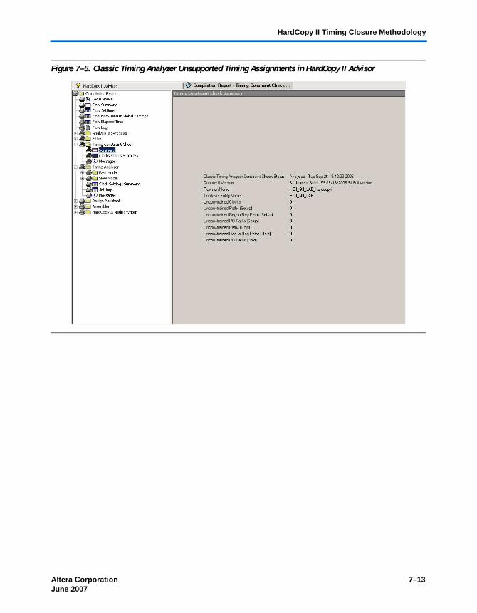
Altera Corporation 7–13June 2007
HardCopy II Timing Closure Methodology
Figure 7–5. Classic Timing Analyzer Unsupported Timing Assignments in HardCopy II Advisor

7–14 Altera Corporation June 2007
HardCopy Series Handbook, Volume 1
The Compilation Report for both the Stratix II and HardCopy II revisions of your project includes a Timing Constraints Check section (Figure 7–6). This section reports all unconstrained paths based on the coverage provided by the timing constraints used in the design. You should examine this report and verify that all internal and I/O paths and all clock domains are constrained for both setup and hold checks.
Figure 7–6. Classic Timing Analyzer Constraints Check in Compilation Report
When using Classic Timing Analyzer, just as when using the TimeQuest timing analyzer, you should review the Quartus II timing report sections in the Compilation Report and resolve all reported timing violations.
Constraining Timing of HardCopy Series Devices
To ensure that the timing of the HardCopy device meets performance goals, the HardCopy Design Center runs static timing analysis on the design database. For this timing analysis to be meaningful, all timing constraints and timing exceptions that you applied to the design for the FPGA implementation, must also be used for the HardCopy implementation. If you did not use timing constraints or you used only partial timing constraints for the design, you must add constraints to
Altera Corporation 7–15June 2007
Constraining Timing of HardCopy Series Devices
make the design fully constrained, and use the same constraints for both FPGA and HardCopy revisions in the flow. If you do not do this, you cannot determine whether the HardCopy series device meets the required timing of the end target system. The SDC format timing constraints can be generated using the Quartus II SDC File Editor which provides line numbering, syntax coloring, and call tips. You can enter timing constraints and exceptions directly or specify them from the Constraints menu. An example of the SDC commands is shown in the following section.
The following constraints must be included:
■ Clock definitions■ Primary input port timing■ Primary output port timing■ Combinational timing■ Timing exceptions
f For information on the SDC editor, refer to the TimeQuest Timing Analyzer chapter in volume 3 of the Quartus II Handbook.
f For more information on timing constraints for the TimeQuest timing analyzer, refer to the TimeQuest Timing Analyzer chapter in volume 3 of the Quartus II Handbook.
f For more information on timing assignments for Classic Timing Analyzer, refer to the Classic Timing Analyzer chapter in volume 3 of the Quartus II Handbook.
Clock Definitions
You can use these definitions to describe the parameters of all different clock domains in a design. Clock parameters that must be defined are frequency, time at which the clock edge rises, time at which the clock edge falls, clock uncertainty (for example: jitter, noise, and designed in timing margin), and clock name. Figure 7–7 illustrates the attributes.

7–16 Altera Corporation June 2007
HardCopy Series Handbook, Volume 1
Figure 7–7. Clock Attributes
The clock settings for PLL clocks are derived automatically based on the PLL settings and reference clock characteristics. You can also override the default PLL clock settings for timing analysis by specifying clock settings for the input clock port on the PLL.
Clock uncertainty in PLL clock outputs is not modeled by default. You should use the set_clock_uncertainty command to model jitter and any other uncertainty and margin in your PLL clocks.
1 Consult with your Altera Field Applications Engineer (FAE) or use MySupport regarding PLL clock uncertainty calculation for your design.
The SDC format provides a simple and easy method to constrain the simplest to the most complex designs. The following example illustrates the simplest SDC commands for a clock (port or pin) and for a generated clock at the PLL output pin for a design:
#Constrain the base clockcreate_clock -period 10.000 [get_ports clkin]
#Constrain the PLL output clockderive_pll_clocks
1 Although derive_pll_clocks is in the sdc_ext package, it is the unique exception to the requirement that all timing constraints in the HardCopy II design flow must be in the sdc package. This command is automatically translated to the sdc-package command generated_pll_clock prior to transfer to the HCDC.
0.0
clk
5.0 10.0
Clock Period = 10.0 nsClock
Uncertainty
0.5- 0.5
Rising Edgeof Clock
Falling Edgeof Clock
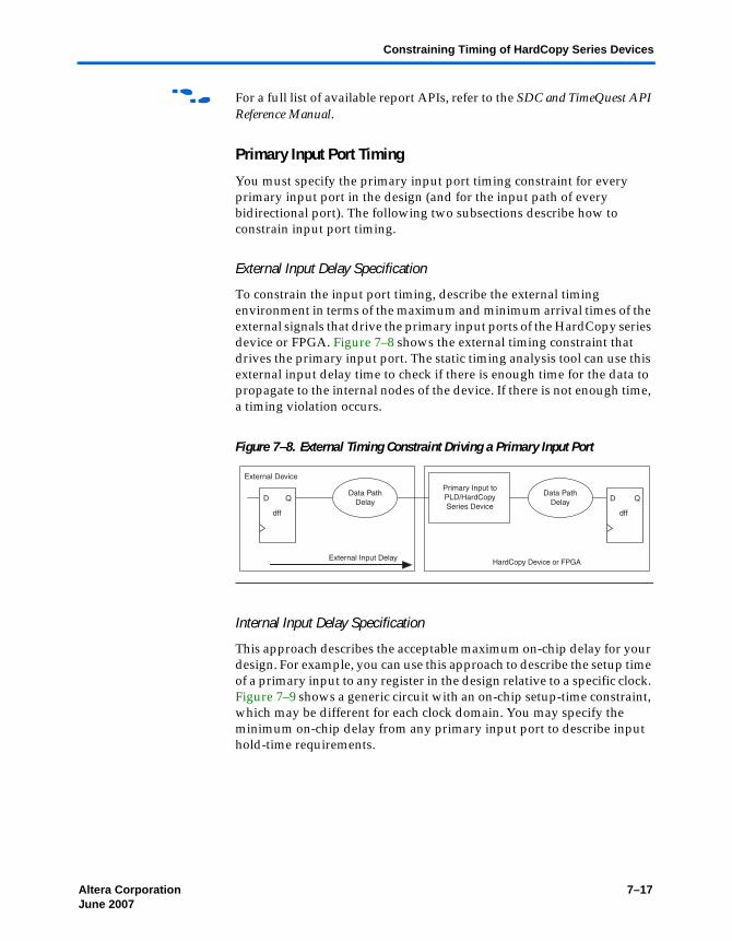
Altera Corporation 7–17June 2007
Constraining Timing of HardCopy Series Devices
f For a full list of available report APIs, refer to the SDC and TimeQuest API Reference Manual.
Primary Input Port Timing
You must specify the primary input port timing constraint for every primary input port in the design (and for the input path of every bidirectional port). The following two subsections describe how to constrain input port timing.
External Input Delay Specification
To constrain the input port timing, describe the external timing environment in terms of the maximum and minimum arrival times of the external signals that drive the primary input ports of the HardCopy series device or FPGA. Figure 7–8 shows the external timing constraint that drives the primary input port. The static timing analysis tool can use this external input delay time to check if there is enough time for the data to propagate to the internal nodes of the device. If there is not enough time, a timing violation occurs.
Figure 7–8. External Timing Constraint Driving a Primary Input Port
Internal Input Delay Specification
This approach describes the acceptable maximum on-chip delay for your design. For example, you can use this approach to describe the setup time of a primary input to any register in the design relative to a specific clock. Figure 7–9 shows a generic circuit with an on-chip setup-time constraint, which may be different for each clock domain. You may specify the minimum on-chip delay from any primary input port to describe input hold-time requirements.
External Device
External Input Delay
Primary Input to PLD/HardCopy Series Device
D Q
dff
D Q
dff
Data Path Delay
Data Path Delay
HardCopy Device or FPGA

7–18 Altera Corporation June 2007
HardCopy Series Handbook, Volume 1
Figure 7–9. Internal Input Delay Specification (Setup)
Figure 7–10 shows a generic circuit with an on-chip hold-time constraint.
Figure 7–10. Internal Input Delay Specification (Hold)
Primary Output Port Timing
You must specify the output port timing constraint for every primary output port in the design and for the output path of every bidirectional port. There are two ways to capture the output port timing, as described in the following two sections.
tsu for a Primary Input Port
data
clk
tsu
Data Path Delay
Clock Delay
tH for a Primary Input
data
clk
tH
Data Path Delay
Clock Delay

Altera Corporation 7–19June 2007
Constraining Timing of HardCopy Series Devices
External Output Delay Specification
One way to capture output port timing is to describe the external timing environment, which is the maximum and minimum delay times of external signals that are driven by the primary output ports of the HardCopy series device. Figure 7–11 shows the external timing constraint driven by the primary output port. The static timing analysis tool uses this information to check that the on-chip timing of the output signals is within the desired specification.
Figure 7–11. External Timing Constraint for a Primary Output Port
Internal Output Delay (Tco) Specification
This approach describes the acceptable maximum and minimum on-chip clock-to-output (TCO) delay. For example, you can use this approach to describe the time it takes from the active edge of the clock to the data arriving at the primary output port. Figure 7–12 shows a generic circuit with an on-chip TCO time constraint. In addition, there can be a minimum TCO requirement.
Figure 7–12. On-Chip Clock-to-Output (Tco) Time Constraint
D Q
dff
D Q
dff
Primary Output from FPGA/HardCopy
Series Device
External Device
External Output Delay
Data Path Delay
Data Path Delay
HardCopy Device or FPGA
tco for a Primary Output Port
clk
Data Path Delay
Clock Delay
tco
output

7–20 Altera Corporation June 2007
HardCopy Series Handbook, Volume 1
Combinational Timing
In combinational timing circuits, a path exists from a primary input port to a primary output port. This type of circuit does not contain any registers. Therefore, it does not require a clock for constraint specification. You only need the maximum and minimum delay from the primary input port to the primary output port to constrain the path for timing requirements. Figure 7–13 shows the placement requirement for a combinational delay arc constraint in a generic circuit.
Figure 7–13. Combinational Timing Constraint
Timing Exceptions
Some circuit structures warrant special consideration. For example, you can ignore all timing paths between two clock domains when a design has more than one clock domain and the clock domains are not related. You can ignore all timing paths using the static timing analysis tool by specifying false paths for all signals that go from one clock domain to the other clock domain(s). Additionally, some circuits are not intended to operate in a single-clock cycle. These circuits require that you specify multi-cycle clock exceptions.
After capturing the information, the Altera HCDC directly checks all timing of the HardCopy series device before tape-out occurs. If any timing violations occur in the HardCopy series device due to overly aggressive timing constraints, Altera must fix them, or you must waive them.
input Data Path Delay
Combinational Delay Arc
output

Altera Corporation 7–21June 2007
Unsupported HardCopy II Timing Constraints for Classic Timing Analyzer
Unsupported HardCopy II Timing Constraints for Classic Timing Analyzer
The Quartus II software supports a wide variety of complex timing constraints. When using Classic Timing Analyzer for HardCopy II design, however, some of these constraints are not translated to SDC format constraints when the design is transferred to the HCDC. The unsupported timing constraints for HardCopy II are listed below:
■ Clock enable multicycle paths■ Inverted clocks■ TSU, Th, TCO, and Min TCO
■ Internal TPD
■ Virtual clocks■ Maximum clock and data skew■ Maximum and minimum delay
If these constraints are used, you can still perform timing analysis in the Quartus II software and produce the correct results. However, when a HardCopy II archive for handoff is created, they will be ignored. The translation of Quartus II timing constraints to SDC constraints simply drops unsupported constraints; they do not feed forward to the HCDC. Any unsupported constraints in a design are listed under the Incompatible Assignments section in the HardCopy II Advisor (see Figure 7–5).
While it is possible to translate unsupported constraints to constraints that are supported, the process is difficult and error-prone, often requiring detailed analysis of the particular context in which the constraint is used.
For this reason, Altera recommends that you use timing constraints in the industry-standard SDC format with the TimeQuest timing analyzer or use only supported timing constraints for Classic Timing Analyzer from the start of your HardCopy II project. This approach avoids any translation or constraint coverage issues that may occur later in a project and the inevitable delay and risk that results.
In some cases, a HardCopy II project in the Quartus II software may already be using the unsupported constraints, and you may choose either to translate the existing, unsupported constraints, or replace them with a new set of constraints that use only the recommended HardCopy II timing assignments. In many cases, you may find it easier to rebuild the constraints rather than translate existing constraints. This is because of the ambiguous nature of many unsupported timing constraints, which often require additional information outside of the Quartus II software before the translation can be properly resolved. Verifying that the translations produce the same timing constraint coverage and the same timing analysis results can also be a time-consuming and error-prone exercise.

7–22 Altera Corporation June 2007
HardCopy Series Handbook, Volume 1
If you do wish to translate existing, unsupported timing constraints to recommended constraints, use Table 7–1 as a rough guide. It shows how values used in TCO, Th, TSU, and Min TCO assignments normally convert to values used in recommended HardCopy II assignments. In the table, unsupported constraints are listed in the left hand column. Recommended constraints are listed along the top row. To use the table, cross-reference the unsupported constraints you wish to translate against a recommended constraint. The cross reference cell contains the conversion of the original, unsupported constraint value that should be used with the new, recommended constraint. It is very important to note that these translations are not valid in every design scenario.
Conclusion This chapter described timing considerations and Quartus II timing constraint recommendations for HardCopy II projects. By understanding these considerations and following the recommendations in your design, you ensure a smooth transition through the Quartus II software and subsequent transfer to the Altera HardCopy Design Center for the back-end design of your structured ASIC. Following the recommendations in this chapter will help ensure success in your HardCopy II project.
Table 7–1. TSU, TH, TCO, and Minimum TCO Timing Constraint Conversion Notes (1), (2), (3), (4), (5)
setup_relationship set_input_delay hold_relationship set_output_delay
TSU Req TSU -max <TCK-TSU>
Th Req -min Th -Th
TCO Req TCO -max <TCK-TCO>
MinTCO
Req
Min TCO -min <- Min TCO>
Note to Table 7–1:(1) TSU = value used in the TSU requirement assignment.(2) TCO = value used in the TCO requirement assignment.(3) Th = value used in the Th requirement assignment.(4) Min TCO = value used in Min TCO requirement assignment.(5) TCK = period of the clock for registers associated with the TSU and TCO requirements.

Altera Corporation 7–23June 2007
Document Revision History
Document Revision History
Table 7–2 shows the revision history for this chapter.
Table 7–2. Document Revision History
Date and Document Version Changes Made Summary of Changes
June 2007, v2.1 Minor text edits.
December 2006 v2.0
Major updates for the Quartus II software version 6.1.0● Added information on TimeQuest timing analyzer, newly
available in Quartus II software version 6.1.0, and recommended for use in HardCopy II design timing analysis.
● Added “Using the TimeQuest Timing Analyzer” section.● Brought in “Constraining Timing of HardCopy Series
Devices” section, previously in Chapter 22.● Updated “HardCopy II Timing Closure Methodology”
section.● Added revision history.
A major update to the chapter, due to changes in the Quartus II software version 6.1 release, especially the inclusion of the TimeQuest timing analyzer; most changes were in the “HardCopy II Timing Closure Methodology” section, and the addition of the “Using the TimeQuest Timing Analyzer” and “Constraining Timing of HardCopy Series Devices”sections.
March 2006, v1.0 Added document to the HardCopy Series Handbook.

7–24 Altera Corporation June 2007
HardCopy Series Handbook, Volume 1

Altera Corporation 8–1June 2007 Preliminary
8. Migrating Stratix II DeviceResources to HardCopy II
Devices
Introduction Altera® HardCopy® II devices and Stratix® II devices are both manufactured on a 1.2-V, 90-nm process technology and offer many similar features. Designers can use the Quartus® II software to migrate their Stratix II design to a HardCopy II device. The Quartus II software ensures that the design revision targeting a HardCopy II device retains the same functionality as the original Stratix II design.
Beginning with version 5.0 of the Quartus II software, you can select a HardCopy II companion device from the Device Settings dialog box (Device menu). Selecting a HardCopy II device as a companion device is similar to adding another Stratix II device in the migration device chain. The Quartus II software compiles the design to use the common resources available in all of the selected Stratix II devices and the selected HardCopy II devices. The HardCopy II companion device becomes the target device when you switch to the HardCopy II flow from this Stratix II flow later in the Quartus II project compilation.
f For more information on compiling with Stratix II and HardCopy II companion revisions using Quartus II software, refer to the Quartus II Support for HardCopy II Devices chapter of the HardCopy Series Devices Handbook.
When you select a HardCopy II companion device, you can set the Quartus II Compiler to limit the design to the minimum resource availability of memory blocks and available logic for digital signal processing (DSP) from either the targeted Stratix II or HardCopy II companion device. Additional limitations also include I/O pin assignments and phase-locked loops (PLLs). This document is a guide for designers migrating Stratix II designs into HardCopy II devices. This document highlights resources that are not supported by the selected Stratix II and HardCopy II companion device pair or any resource differences between Stratix II devices and the HardCopy II device.
This document includes the following topics:
■ Stratix II and HardCopy II Migration Options■ I/O Support and Planning ■ External Memory Interface Support■ On-Chip Termination■ Stratix II and HardCopy II Companion Memory Blocks■ PLL Planning and Utilization
H51024-1.3

8–2 Altera CorporationJune 2007
HardCopy Series Handbook, Volume 1
■ Global and Local Signals■ Stratix II ALM Adaptation into HardCopy II Logic■ HardCopy II DSP Implementation from Stratix II DSP Blocks■ JTAG BST and Extended Functions■ Power Up and Configuration Compatibility
Stratix II and HardCopy II Migration Options
The Quartus II software allows you to migrate between different Stratix II devices in the same package. When compiling Stratix II designs in the Quartus II software, you can specify one Stratix II target device and one or more Stratix II migration devices. When you specify at least one migration device, the Quartus II Compiler constrains the overall design’s I/O pins and other resource assignments to the minimum resources available in any of the selected migration devices. This feature allows vertical migration between devices using the same package footprint. To create the proper configuration file for one of the Stratix II devices selected in the migration devices menu, select that device as a target device.
The introduction of HardCopy II provides an additional seamless migration path for Stratix II devices. After you select a particular Stratix II device, the Quartus II software provides migration options in the Settings dialog box. For example, if your design targets the EP2S130 device in the 1,020-pin FineLine BGA® package, the Quartus II software provides the EP2S90 and EP2S180 devices in the 1,020-pin FineLine BGA package as migration options as well as the HC230 device in the 1,020-pin FineLine BGA package.
Conversely, the HardCopy II architecture allows you to design a structured ASIC and then prototype with a wide range of Stratix II devices. If the target device is a HardCopy II HC220 device in the 780-pin FineLine BGA package, you can select the Stratix II EP2S90 or EP2S130 device in the 780-pin FineLine BGA package as prototype devices. Table 8–1 shows vertical migration options by package.

Altera Corporation 8–3June 2007 Preliminary
Stratix II and HardCopy II Migration Options
Beginning with version 5.0 of the Quartus II software, when you compile a design targeting a HardCopy II device, you will need to select a target Stratix II device and a HardCopy II companion device for compilation. Table 8–2 lists the available HardCopy II and Stratix II companion pairs. These pairs are retained in most resource availability tables in this chapter to show the maximum resources available that are supported by either device of the companion pair.
Table 8–1. Stratix II and HardCopy II Migration Options Note (1)
DeviceFineLine BGA Package
484 Pins 672 Pins 780 Pins 1,020 Pins 1,020 Pins 1,508 Pins
HardCopy II HC210 HC220 HC220 HC230 HC240 HC240
Stratix II EP2S30EP2S60
EP2S90(2)
EP2S60 EP2S90EP2S130
EP2S90EP2S130EP2S180
EP2S180 EP2S180
Notes to Table 8–1:(1) Table 8–1 does not include the HC210W device. For information on the HC210W device, contact the Altera
Applications Group.(2) This is a Hybrid FineLine BGA package. For more details, refer to the Package Information for Stratix II Devices
chapter in volume 2 of the Stratix Device Handbook.
Table 8–2. Stratix II and HardCopy II Companion Devices (Part 1 of 2) Note (1)
PackageCompanion Pair
HardCopy II Device Stratix II Device
484-pin FineLine BGA HC210 EP2S30
484-pin FineLine BGA HC210 EP2S60
484-pin Hybrid FineLine BGA HC210 EP2S90(2)
672-pin FineLine BGA HC220 EP2S60
780-pin FineLine BGA HC220 EP2S90
780-pin FineLine BGA HC220 EP2S130
1,020-pin FineLine BGA HC230 EP2S90
1,020-pin FineLine BGA HC230 EP2S130

8–4 Altera CorporationJune 2007
HardCopy Series Handbook, Volume 1
When the Quartus II software successfully compiles a design, the HardCopy II Device Resource Guide in the Fitter Compilation Report contains information on migration compatibility to a HardCopy II device. Use this information to select the optimal HardCopy II device for the prototype Stratix II device based on resource requirements and package preference.
Table 8–3 shows the available resources for prototyping on a Stratix II device when choosing a HardCopy II device. This chapter examines each resource availability in greater detail.
1,020-pin FineLine BGA HC230 EP2S180
1,020-pin FineLine BGA HC240 EP2S180
1,508-pin FineLine BGA HC240 EP2S180
Notes to Table 8–2:(1) Table 8–2 does not include the HC210W device. For information on the HC210W
device, contact the Altera Applications Group.(2) This is a Hybrid FineLine BGA package. For more details, refer to the Package
Information for Stratix II Devices chapter in volume 2 of the Stratix Device Handbook.
Table 8–2. Stratix II and HardCopy II Companion Devices (Part 2 of 2) Note (1)
PackageCompanion Pair
HardCopy II Device Stratix II Device
Table 8–3. Stratix II and HardCopy II Companion Devices Resource Availability Guide (Part 1 of 2) Note (1)
Stratix II and
HardCopy II Companion
Devices
PackageStratix II
ALMs (2)
HardCopy II Prototyping Resources
ASIC Gates for
Logic
User I/O Pins
(3)
M4K Blocks
M-RAM Blocks
Total RAM Bits
18 × 18 Multipliers PLLs
EP2S30HC210
484-pin FineLine BGA
13,552 360K 334 144 0 663,552 64 4
EP2S60HC210
484-pin FineLine BGA
24,176 720K 334 190 0 875,520 144 4
EP2S90HC210
484-pin FineLine BGA
36,384 1 M 308 190 0 875,520 192 4
EP2S60HC220
672-pin FineLine BGA
24,176 720K 492 255 2 2,354,688 144 4
EP2S90HC220
780-pin FineLine BGA
36,384 1 M 494 408 2 3,059,712 192 4

Altera Corporation 8–5June 2007 Preliminary
I/O Support and Planning
I/O Support and Planning
HardCopy II companion devices offer pin-to-pin compatibility with the Stratix II prototype device, which makes them drop-in replacements for the FPGAs. Therefore, you can use HardCopy II devices with the same system board and software developed for prototyping and field trials, enabling the fastest time-to market for high-volume production.
HardCopy II devices offer up to 951 user I/O pins. Table 8–4 lists all available I/O pin counts when assigning a Stratix II device while selecting a HardCopy II companion device. If a Stratix II design uses I/O pins that are not available in both the Stratix II device and the HardCopy II companion device, the Quartus II software issues a no-fit error. Therefore, it is important to monitor pin assignments based on the Stratix II device and the HardCopy II companion device.
EP2S130HC220
780-pin FineLine BGA
53,016 1.6 M 494 408 2 3,059,712 252 4
EP2S90HC230
1,020-pin FineLine BGA
36,384 1 M 698 408 4 4,239,360 192 8
EP2S130HC230
1,020-pin FineLine BGA
53,016 1.6 M 698 609 6 6,345,216 252 8
EP2S180HC230
1,020-pin FineLine BGA
71,760 2.2 M 698 614 6 6,368,256 384 8
EP2S180HC240
1,020-pin FineLine BGA
71,760 2.2 M 742 768(4) 9 8,847,360 384 12
EP2S180HC240
1,508-pin FineLine BGA
71,760 2.2 M 951 768(4) 9 8,847,360 384 12
Notes to Table 8–3:(1) Table 8–3 does not include the HC210W device. For information on the HC210W device, contact the Altera
Applications Group.(2) ALM: adaptive logic module.(3) User I/O pin counts are preliminary. The Quartus II software I/O pin counts include one additional pin, PLL_ENA,
which is not included in this pin count.(4) The total number of usable M4K blocks is limited to 768 to allow migration compatibility when prototyping with
an EP2S180 device.
Table 8–3. Stratix II and HardCopy II Companion Devices Resource Availability Guide (Part 2 of 2) Note (1)
Stratix II and
HardCopy II Companion
Devices
PackageStratix II
ALMs (2)
HardCopy II Prototyping Resources
ASIC Gates for
Logic
User I/O Pins
(3)
M4K Blocks
M-RAM Blocks
Total RAM Bits
18 × 18 Multipliers PLLs

8–6 Altera CorporationJune 2007
HardCopy Series Handbook, Volume 1
HardCopy II devices offer three distinct types of I/O elements (IOEs) which support a variety of I/O features to match Stratix II IOEs. These are memory interface IOEs, high-speed IOEs, and general purpose IOEs.
Memory interface IOEs support popular I/O standards used by external memory devices, including single-ended standards from LVTTL, LVCMOS to SSTL, and HSTL voltage referenced (VREF) type I/O standards. Memory interface IOEs also have PCI clamp circuitry for PCI support.
High-speed IOEs support differential applications utilizing LVDS and HyperTransport technology. High-speed IOEs also support single-ended LVTTL and LVCMOS I/O standards, but do not support VREF I/O standards.
General purpose IOEs support LVTTL and LVCMOS I/O standards. General purpose IOEs on the bottom I/O banks (banks 7 and 8) also have PCI clamping circuitry to support the PCI interface on HardCopy II devices.
Table 8–4. Package Options and I/O Pin Counts for Stratix II and HardCopy II Companion Devices Notes (1), (2)
Stratix II Device
HC210 HC220 HC230 (3) HC240 (4)
484-Pin FineLine BGA
672-Pin FineLine BGA
780-Pin FineLine BGA
1,020-Pin FineLine BGA
1,020-Pin FineLine BGA
1,508-Pin FineLine BGA
EP2S30 334
EP2S60 334 492
EP2S90 308 494 698
EP2S130 494 698
EP2S180 698 742 951
Notes to Table 8–4:(1) User I/O pin counts are preliminary. The Quartus II software I/O pin counts include one additional pin, PLL_ENA,
which is not included in this pin count. The PLL_ENA pin is not available as a general purpose I/O pin and can only be used to enable the PLLs in this device.
(2) All I/O pin counts include eight dedicated clock input pins (clk1p, clk1n, clk3p, clk3n, clk9p, clk9n, clk11p, and clk11n) that can be used for data inputs.
(3) The I/O pin counts for all HC230 combinations include four dedicated fast PLL clock inputs (FPLL7CLKp/n, FPLL8CLKp/n) that can be used for data inputs.
(4) The I/O pin counts for HC240 combinations include eight dedicated fast PLL clock inputs (FPLL7CLKp/n, FPLL8CLKp/n, FPLL9CLKp/n, and FPLL10CLKp/n) that can be used for data inputs.

Altera Corporation 8–7June 2007 Preliminary
I/O Support and Planning
f For more information on HardCopy II IOEs, refer to the HardCopy II Description, Architecture, and Features chapter of the HardCopy Series Handbook.
HardCopy II I/O Banks
HardCopy II devices have eight general I/O banks and up to four enhanced PLL external clock output banks (banks 9, 10, 11, 12). HC210 and HC220 devices only have PLL output banks 9 and 10. Figure 8–1 shows the HardCopy II I/O banks and the relative PLL positions.
The left side I/O banks 1 and 2 are high speed IOE banks on all HardCopy II devices. The right side I/O banks 5 and 6 are general purpose IOEs on HC210, HC220, and HC230 devices, but high speed IOEs on HC240 devices.
The top I/O banks 3 and 4 are memory interface IOEs on all HardCopy II devices. The bottom I/O banks 7 and 8 are general purpose IOEs on HC210 and HC220 but memory interface IOEs on HC230 and HC240 devices. The general purpose IOEs on the bottom of the device support PCI clamping, but the general purpose IOEs on the right side do not.

8–8 Altera CorporationJune 2007
HardCopy Series Handbook, Volume 1
Figure 8–1. HardCopy II HC240 I/O Banks Notes (1), (2), (3), (4)
Notes to Figure 8–1:(1) Figure 8–1 is a top view of the silicon die that corresponds to a reverse view for flip-chip packages. It is a graphical
representation only. Refer to the pin list and Quartus II software for exact locations.(2) Differential HSTL and differential SSTL standards are available for bidirectional operations on DQS pin and input
only operations on PLL clock input pins; LVDS, LVPECL, and HyperTransport standards are available for input only operations on PLL clock input pins. Refer to “Differential I/O Termination” on page 8–20 for more details.
(3) HardCopy II devices and the Quartus II software does not support differential SSTL and differential HSTL standards at left and right I/O banks. Side I/O banks do not have VREF pins.
(4) Figure 8–1 shows the HC240 device. Other HardCopy II devices have fewer PLL blocks.
Bank 4Memory Interface IOEs
Bank 7Memory Interface IOEs
Bank 8Memory Interface IOEs
I/O banks 3 & 4 support 3.3-V, 2.5-V, 1.8-V LVTTL/LVCMOS, 1.5-V LVCMOS, SSTL-2, SSTL-18, 1.8-V
HSTL, 1.5-V HSTL & PCI/PCI-X I/O standards.
I/O banks 7 & 8 support 3.3-V, 2.5-V, 1.8-V LVTTL/LVCMOS, 1.5-V LVCMOS & PCI/PCI-X I/O standards.
Bank 3Memory Interface IOEs
Bank 2High-Speed IOEs
Bank 1High-Speed IOEs
Bank 5High-Speed IOEs
Bank 6High-Speed IOEs
PLL 1
PLL 2
PLL 4
PLL 3
I/O Banks 5 & 6 Support 3.3-, 2.5- & 1.8-V LVTTL/LVCMOS,
1.5-V LVCMOS, LVDS & HyperTransport Technology
I/O Banks 1 & 2 Support 3.3-, 2.5- & 1.8-V LVTTL/LVCMOS,1.5-V LVCMOS, LVDS & HyperTransport Technology
CLK, PLL_FB input pins & PLL_OUT output pins support differential SSTL, differential HSTL,
LVDS & HyperTransport technology. CLK & PLL_FB pins support LVPECL. DQS input pins support
differential SSTL and differential HSTL I/O standards.
CLK, PLL_FB input pins SSTL-2, SSTL-18, 1.8-V HSTL, 1.5-V HST, & PLL_OUT output
pins support differential SSTL, differential HSTL, LVDS & HyperTransport technology. CLK & PLL_FB
pins support LVPECL. DQS input pins supportdifferential SSTL and differential HSTL I/O standards.
PLL 5PLL 11
Bank 11 Bank 9
PLL 6PLL 12
Bank 12 Bank 10
PLL 10
PLL 9
PLL 7
PLL 8

Altera Corporation 8–9June 2007 Preliminary
I/O Support and Planning
User I/O Count Per IOE Type and Bank Location
Table 8–5 lists the maximum I/O count per IOE type. This helps you select a HardCopy II device based on the I/O standard support requirement.
HardCopy II Supported I/O Standards
Table 8–6 lists I/O standards that HardCopy II devices supports, separated by IOE type. This list only focuses on user I/O pins.
Table 8–5. HardCopy II Maximum User I/O Count Per IOE Type Notes (1), (2)
Device Package
Memory Interface IOEs
General Purpose IOEs High-Speed IOEs
Top Bottom Right Bottom Left Right
HC210 484-pin FineLine BGA 87 84 79 84
HC220 672-pin FineLine BGA 126 124 118 124
HC220 780-pin FineLine BGA 126 124 120 124
HC230 (3) 1,020-pin FineLine BGA 180 178 152 188
HC240 (4) 1,020-pin FineLine BGA 184 182 188 188
HC240 (4) 1,508-pin FineLine BGA 238 233 240 240
Notes to Table 8–5:(1) User I/O pin counts are preliminary. The Quartus II software I/O pin counts include one additional pin, PLL_ENA,
which is not included in this pin count. The PLL_ENA pin is not available as a general purpose I/O pin and can only be used to enable the PLLs in this device.
(2) All I/O pin counts include eight dedicated clock input pins (clk1p, clk1n, clk3p, clk3n, clk9p, clk9n, clk11p, and clk11n) that can be used for data inputs.
(3) The I/O pin counts for all HC230 combinations include four dedicated fast PLL clock inputs (FPLL7CLKp/n, FPLL8CLKp/n) that can be used for data inputs.
(4) The I/O pin counts for HC240 combinations include eight dedicated fast PLL clock inputs (FPLL7CLKp/n, FPLL8CLKp/n, FPLL9CLKp/n, and FPLL10CLKp/n) that can be used for data inputs.
Table 8–6. Hardcopy II Supported I/O Standards on User I/O Pins (Part 1 of 2)
I/O Standard TypeVCCIO Level (V) Memory
Interface IOEs
General Purpose
IOEs
High-Speed IOEsInput Output
3.3-V LVTTL/LVCMOS Single-ended 3.3/2.5 3.3 v v v
2.5-V LVTTL/LVCMOS Single-ended 3.3/2.5 2.5 v v v
1.8-V LVTTL/LVCMOS Single-ended 1.8/1.5 1.8 v v v
1.5-V LVCMOS Single-ended 1.8/1.5 1.5 v v v

8–10 Altera CorporationJune 2007
HardCopy Series Handbook, Volume 1
SSTL-2 class I and II Voltage referenced 2.5 2.5 v
SSTL-18 class I and II Voltage referenced 1.8 1.8 v
1.8-V HSTL class I and II Voltage referenced 1.8 1.8 v
1.5-V HSTL class I and II Voltage referenced 1.5 1.5 v
PCI / PCI-X Single-ended 3.3 3.3 v (1)
Differential SSTL-2 class I and II input
Pseudo differential (3) 3.3/2.5/1.8/1.5
(2)
Differential SSTL-2 class I and II output
Pseudo differential (3) 2.5 (2)
Differential SSTL-18 class I and II input
Pseudo differential (3) 3.3/2.5/ 1.8/1.5
(2)
Differential SSTL-18 class I and II output
Pseudo differential (3) 1.8 (2)
1.8-V differential HSTL class I and II input
Pseudo differential (3) 3.3/2.5/ 1.8/1.5
1.8/1.5 (2)
1.8-V differential HSTL class I and II output
Pseudo differential (3) 1.8 (2)
1.5-V differential HSTL class I and II input
Pseudo differential (3) 3.3/2.5/ 1.8/1.5
(2)
1.5-V differential HSTL class I and II output
Pseudo differential (3) 1.5 (2)
LVDS Differential 2.5 2.5 v
HyperTransport™ technology
Differential 2.5 2.5v
Notes to Table 8–6:(1) Like Stratix II devices, the optional PCI clamp is only available on column I/O pins. General purpose IOEs on the
right row I/O pins do not support the PCI clamp.(2) Similar to Stratix II devices, these I/O standards are only available on input clock pins, output clock pins in I/O
banks 9, 10, 11, 12, and DQS pins in top I/O banks 3, 4 for all HardCopy II devices, and DQS pins in bottom I/O banks 7 and 8 for HC230 and HC240 devices.
(3) Pseudo-differential HSTL and SSTL inputs only use the positive polarity input in the speed path. The negative input is not connected internally. Pseudo-differential HSTL and SSTL outputs use two single-ended outputs with the second output programmed as inverted. This is similar to a Stratix II device implementation.
Table 8–6. Hardcopy II Supported I/O Standards on User I/O Pins (Part 2 of 2)
I/O Standard TypeVCCIO Level (V) Memory
Interface IOEs
General Purpose
IOEs
High-Speed IOEsInput Output

Altera Corporation 8–11June 2007 Preliminary
I/O Support and Planning
Table 8–7 lists the I/O standards that HardCopy II devices support. Table 8–7 is organized by clock input, clock output, and PLL feedback pins.
Table 8–7. Hardcopy II Supported I/O Standards of Input Clocks, Clock Out, and PLL Feedback (Part 1 of 2)
I/O Standard TypeVCCIO Level (V) CLK[0..3,
8..11] (1)
CLK[4..7, 12..15]
(2)
FPLL_CLK (3)
PLL_OUT (4)
PLL_FB (5)Input Output
3.3-V LVTTL / LVCMOS
Single-ended
3.3/2.5 3.3v v v v v
2.5-V LVTTL / LVCMOS
Single-ended
3.3/2.5 2.5v v v v v
1.8-V LVTTL / LVCMOS
Single-ended
1.8/1.5 1.8v v v v v
1.5-V LVCMOS Single-ended
1.8/1.5 1.5v v v v v
SSTL-2 class I Voltage referenced
2.5 2.5v v v
SSTL-2 class II Voltage referenced
2.5 2.5v v v
SSTL-18 class I Voltage referenced
1.8 1.8v v v
SSTL-18 class II Voltage referenced
1.8 1.8v v v
1.8-V HSTL class I
Voltage referenced
1.8 1.8v v v
1.8-V HSTL class II
Voltage referenced
1.8 1.8v v v
1.5-V HSTL class I
Voltage referenced
1.5 1.5v v v
1.5-V HSTL class II
Voltage referenced
1.5 1.5v v v
PCI / PCI-X Single-ended
3.3 3.3v v v
Differential SSTL-2 class I and II input
Pseudo differential
(6)
3.3/2.5/ 1.8/1.5 v v
Differential SSTL-2 class I and II output
Pseudo differential
(6)
2.5v v
Differential SSTL-18 class I and II input
Pseudo differential
(6)
3.3/2.5/ 1.8/1.5 v v

8–12 Altera CorporationJune 2007
HardCopy Series Handbook, Volume 1
Differential SSTL-18 class I and II output
Pseudo differential
(6)
1.8v v
1.8-V differential HSTL class I and II input
Pseudo differential
(6)
3.3/2.5/ 1.8/1.5 v v
1.8-V differential HSTL class I and II output
Pseudo differential
(6)
1.8v v
1.5-V differential HSTL class I and II input
Pseudo differential
(6)
3.3/2.5/ 1.8/1.5 v v
1.5-V differential HSTL class I and II output
Pseudo differential
(6)
1.5v v
LVDS input Differential 2.5 v v v v
LVDS output Differential 2.5 v v
HyperTransport technology input
Differential 2.5v v v v
HyperTransport technology output
Differential 2.5Vv v
LVPECL input Differential 3.3/2.5/ 1.8/1.5
(7)v v v
Notes to Table 8–7:(1) CLK8 and CLK10 pins on HC210, HC220, and HC230 devices do not support differential standards LVDS and
HyperTransport technology. Only LVTTL is supported on these CLK pins for these devices.(2) CLK[4..7] pins on HC210 and HC220 devices do not support SSTL, HSTL, differential SSTL, and HSTL input or
output.(3) HC230 only has two fast PLL clocks, FPLL[7..8]CLK. HC240 has four FPLL clocks, FPLL[7..10]CLK.(4) HC210 and HC220 PLL6_OUT pins do not support SSTL, HSTL, differential SSTL, and HSTL input or output.(5) HC210 and HC220 PLL6_FB pins do not support SSTL, HSTL, differential SSTL, and HSTL input or output.(6) Pseudo-differential HSTL and SSTL inputs only use the positive polarity input in the speed path. The negative
input is not connected internally. Pseudo-differential HSTL and SSTL outputs use two single-ended outputs with the second output programmed as inverted. This is similar to a Stratix II device implementation.
(7) This is not supported.
Table 8–7. Hardcopy II Supported I/O Standards of Input Clocks, Clock Out, and PLL Feedback (Part 2 of 2)
I/O Standard TypeVCCIO Level (V) CLK[0..3,
8..11] (1)
CLK[4..7, 12..15]
(2)
FPLL_CLK (3)
PLL_OUT (4)
PLL_FB (5)Input Output

Altera Corporation 8–13June 2007 Preliminary
External Memory Interface Support
External Memory Interface Support
Like Stratix II devices, HardCopy II I/O pins have dedicated phase-shift circuitry for interfacing with external memory, including DDR and DDR2 SDRAM, QDR II SRAM, RLDRAM II, and SDR SDRAM. A compensated delay element on each DQS pin automatically aligns input DQS synchronization signals with the data window of their corresponding DQ data signals.
For all HardCopy II devices, the top I/O banks (3 and 4) support DQ and DQS signals with DQ bus modes that vary from ×4, ×8/×9, ×16/×18 and up to ×32/×36. The top bank has a phase-shifting reference circuit that controls the compensated delay elements for all DQS pins on the top bank.
For the HC230 and HC240 HardCopy II devices, the bottom I/O banks (7 and 8) also support DQ and DQS signals with DQ bus modes from ×4, ×8/×9, ×16/×18 and ×32/×36. Similar to the top banks, the bottom I/O banks of these devices also have a phase-shifting reference circuit to control the delay elements at the bottom DQS pins.
Table 8–8 shows the number of DQ and DQS buses supported per companion device pair. (3)
Table 8–8. DQ and DQS Bus Mode support for Stratix II and HardCopy II Companion Devices (Part 1 of 2) Note (1)
Stratix II and HardCopy II
Companion DevicesPackage Number of ×4
GroupsNumber of
×8/×9 Groups
Number of ×16/×18 Groups
Number of ×32/×36 Groups
EP2S30HC210 (2)
484-pin FineLine BGA 4 2
EP2S60HC210 (2)
484-pin FineLine BGA 4 2
EP2S90HC210 (2)
484-pin FineLine BGA 4 2
EP2S60HC220 (2)
672-pin FineLine BGA 9 4 2
EP2S90HC220 (2)
780-pin FineLine BGA 9 4 2
EP2S130HC220 (2)
780-pin FineLine BGA 9 4 2
EP2S90HC230 (3)
1,020-pin FineLine BGA 36 18 8 4
EP2S130HC230 (3)
1,020-pin FineLine BGA 36 18 8 4

8–14 Altera CorporationJune 2007
HardCopy Series Handbook, Volume 1
LVDS, SERDES, and DPA Compatibility
HardCopy II devices offer up to 116 transmitter and receiver pairs. Similar to Stratix II devices, these differential I/O pins are located on row I/O pins. The HC240 device’s left and right banks are high-speed IOEs which support differential transmission. The HC210, HC220, and HC230 devices only support differential transmission on the left banks. The LVDS and HyperTransport technology interface functionality, including the SERDES and DPA, is the same as Stratix II devices.
Table 8–9 shows the maximum differential channel supported by each HardCopy II and Stratix II companion pair.
EP2S180HC230 (3)
1,020-pin FineLine BGA 36 18 8 4
EP2S180HC240
1,020-pin FineLine BGA 36 18 8 4
EP2S180HC240
1,508-pin FineLine BGA 36 18 8 4
Notes to Table 8–8:(1) The DQ and DQS numbers are preliminary.(2) HardCopy II devices HC210 and HC220 support memory interface in the top I/O banks only. Unlike their Stratix II
companions, these devices cannot support DIMMs.(3) Similar to their Stratix II companions, these device and package combinations can support two 64- or 72-bit DIMMs
in ×4 and ×8/×9 modes.
Table 8–8. DQ and DQS Bus Mode support for Stratix II and HardCopy II Companion Devices (Part 2 of 2) Note (1)
Stratix II and HardCopy II
Companion DevicesPackage Number of ×4
GroupsNumber of
×8/×9 Groups
Number of ×16/×18 Groups
Number of ×32/×36 Groups
Table 8–9. Differential Channels with Stratix II and HardCopy II Companion Devices (Part 1 of 2) Note (1)
Stratix II and HardCopy II
Companion DevicesPackage Transmitters Receivers
EP2S30HC210 (2)
484-pin FineLine BGA 19 21
EP2S60HC210 (2)
484-pin FineLine BGA 19 21
EP2S90HC210 (2)
484-pin FineLine BGA 19 21

Altera Corporation 8–15June 2007 Preliminary
External Memory Interface Support
Programmable Drive Strength Support
The maximum current strength setting is the default setting in the Quartus II software and achieves maximum I/O performance. Stratix II device output buffers for each I/O pin have a programmable drive strength control for certain I/O standards.
HardCopy II support for these settings differs from that found in Stratix II devices. For compatibility with HardCopy II HC210 and HC220 devices, you must restrict the I/O drive settings of Stratix II companion devices, as shown in Table 8–10.
EP2S60HC220 (2)
672-pin FineLine BGA 29 31
EP2S90HC220 (2)
780-pin FineLine BGA 29 31
EP2S130HC220 (2)
780-pin FineLine BGA 29 31
EP2S90HC230 (2)
1,020-pin FineLine BGA 44 46
EP2S130HC230 (2)
1,020-pin FineLine BGA 44 46
EP2S180HC230 (2)
1,020-pin FineLine BGA 44 46
EP2S180HC240 (3)
1,020-pin FineLine BGA 88 92
EP2S180HC240 (3)
1,508-pin FineLine BGA 116 116
Notes to Table 8–9:(1) Pin count does not include dedicated PLL input and output pins. (2) The total number of receiver channels for HC210, HC220, and HC230 devices
include two non-dedicated clock channels that can optionally be used as data channels.
(3) The total number of receiver channels for HC240 devices include four non-dedicated clock channels that can optionally be used as data channels.
Table 8–9. Differential Channels with Stratix II and HardCopy II Companion Devices (Part 2 of 2) Note (1)
Stratix II and HardCopy II
Companion DevicesPackage Transmitters Receivers

8–16 Altera CorporationJune 2007
HardCopy Series Handbook, Volume 1
Table 8–10. HC210 and HC220 Device Programmable Drive Strengths
I/O Standard
IOH and IOL Current Strength Setting
(mA) for Top Column I/O Pins
IOH and IOL Current Strength Setting (mA) for Bottom Column I/O Pins
IOH and IOL Current Strength Setting
(mA) for Left Row I/O Pins
IOH and IOL Current Strength Setting
(mA) for Right Row I/O Pins
3.3-V LVTTL 24, 20, 12, 8, 4 (1) 12, 8, 4 (1) 12, 8, 4 12, 8, 4
3.3-V LVCMOS 24, 20, 12, 8, 4 (1) 8, 4 (1) 8, 4 8, 4
2.5-V LVTTL/LVCMOS 16, 12, 8, 4 12, 8, 4 (1) 12, 8, 4 12, 8, 4
1.8-V LVTTL/LVCMOS 12, 10, 8, 6, 4, 2 8, 6, 4, 2 (1) 8, 6, 4, 2 8, 6, 4, 2
1.5-V LVCMOS 8, 6, 4, 2 4, 2 (1) 4, 2 4, 2
SSTL-2 class I 12, 8 (2) (3) (3)
SSTL-2 class II 24, 20, 16 (2) (3) (3)
SSTL-18 class I 12, 10, 8, 6, 4 (2) (3) (3)
SSTL-18 class II 20, 18, 16, 8 (2) - -
HSTL-18 class I 12, 10, 8, 6, 4 (2) - -
HSTL-18 class II 20, 18, 16 (2) - -
HSTL-15 class I 12, 10, 8, 6, 4 (2) - -
HSTL-15 class II 20, 18, 16 (2) - -
Notes to Table 8–10:(1) HardCopy II devices do not support some of the settings available in the Stratix II prototype device. For more
information, refer to the Stratix II Device Family Data Sheet in volume 1 of the Stratix II Device Handbook.(2) HC220 and HC210 devices do not support memory interface standards on bottom I/O pins.(3) Row I/O pins do not support SSTL I/O standards.

Altera Corporation 8–17June 2007 Preliminary
On-Chip Termination
Similarly, when using HardCopy II HC230 and HC240 devices as companion devices, you must restrict the I/O drive settings, as shown in Table 8–11.
On-Chip Termination
Like Stratix II devices, HardCopy II devices feature on-chip termination (OCT) to provide I/O impedance matching and termination capabilities. To maintain compatibility with Stratix II prototype devices, HardCopy II devices support on-chip series termination (RS) for single-ended I/O standards and on-chip differential termination (RD) for differential I/O standards. However, some HardCopy II pins do not support the on-chip termination that may be available on the same Stratix II pin. This section highlights the termination schemes that HardCopy II devices support.
Table 8–11. HC230 and HC240 Device Programmable Drive Strengths
I/O StandardIOH and IOL Current
Strength Setting (mA) for Column I/O Pins
IOH and IOL Current Strength Setting (mA) for
Row I/O Pins
3.3-V LVTTL 24, 20, 16, 12, 8, 4 (1) 12, 8, 4
3.3-V LVCMOS 24, 20, 16, 12, 8, 4 (1) 8, 4
2.5-V LVTTL/LVCMOS 16, 12, 8, 4 12, 8, 4
1.8-V LVTTL/LVCMOS 12, 10, 8, 6, 4, 2 8, 6, 4, 2
1.5-V LVCMOS 8, 6, 4, 2 4, 2
SSTL-2 class I 12, 8 (2)
SSTL-2 class II 24, 20, 16 (2)
SSTL-18 class I 12, 10, 8, 6, 4 (2)
SSTL-18 class II 20, 18, 16, 8 -
HSTL-18 class I 12, 10, 8, 6, 4 -
HSTL-18 class II 20, 18, 16 -
HSTL-15 class I 12, 10, 8, 6, 4 -
HSTL-15 class II 20, 18, 16 -
Notes to Table 8–11:(1) HardCopy II devices do not support some of the settings available in the Stratix II
prototype device. For more information, refer to the Stratix II Device Family Data Sheet in volume 1 of the Stratix II Device Handbook.
(2) Row I/O pins do not support SSTL I/O standards.

8–18 Altera CorporationJune 2007
HardCopy Series Handbook, Volume 1
On-Chip Series Termination
Stratix II and HardCopy II devices support I/O driver on-chip series termination (RS) through drive-strength control for single-ended I/O standards. There are two ways to implement the RS in Stratix II and Hardcopy II devices:
■ RS without calibration for both row and column I/O pins■ RS with calibration only for column I/O pins
On-Chip Series Termination without Calibration
HardCopy II devices support output-driver impedance matching to closely match the impedance of the transmission line. If you select matching impedance, you cannot select programmable-current drive strength. Table 8–12 lists the HardCopy II HC230 and HC240 output standards that support on-chip series termination without calibration.
Table 8–12. HC230 and HC240 Selectable I/O Drivers with On-Chip Series Termination without Calibration Note (1)
I/O Standard Column I/O Pins Row I/O Pins
3.3-V LVTTL 25 or 50 Ω 25 or 50 Ω
3.3-V LVCMOS 25 or 50 Ω 25 or 50 Ω
2.5-V LVTTL 25 or 50 Ω 25 or 50 Ω
2.5-V LVCMOS 25 or 50 Ω 25 or 50 Ω
1.8-V LVTTL 25 or 50 Ω 50 Ω
1.8-V LVCMOS 25 or 50 Ω 50 Ω
1.5-V LVTTL 50 Ω
1.5-V LVCMOS 50 Ω
2.5-V SSTL class I 50 Ω (2)
2.5-V SSTL class II 25 Ω (2)
1.8-V SSTL class I 50 Ω (2)
1.8-V SSTL class II 25 Ω
1.8-V HSTL class I 50 Ω (2)
1.8-V HSTL class II 25 Ω
1.5-V HSTL class I (3)
Notes to Table 8–12:(1) These numbers are preliminary and pending silicon characterization.(2) HardCopy II HC230 and HC240 devices do not support on-chip series
termination with this I/O standard on these pins.(3) Support pending HardCopy II characterization.

Altera Corporation 8–19June 2007 Preliminary
On-Chip Termination
Table 8–13 lists the HardCopy II HC210 and HC220 output standards that support on-chip series termination without calibration.
On-Chip Series Termination with Calibration
Stratix II devices support on-chip series termination with calibration in column I/O pins in the top and bottom banks. HC230 and HC240 devices also support on-chip series termination with calibration in column I/O pins in the top and bottom banks, but HC220 and HC210 devices only support this feature on the top I/O banks. Table 8–14 lists available I/O standards on the HardCopy II devices that support calibrated-series termination.
Table 8–13. HC210 and HC220 Selectable I/O Drivers with On-Chip Series Termination without Calibration Note (1)
I/O Standard Top Column I/O Pins
Bottom Column I/O Pins Left Row I/O Pins Right Row I/O Pins
3.3-V LVTTL 25 or 50 Ω 25 or 50 Ω 25 or 50 Ω 25 or 50 Ω
3.3-V LVCMOS 25 or 50 Ω 25 or 50 Ω 25 or 50 Ω 25 or 50 Ω
2.5-V LVTTL 25 or 50 Ω 25 or 50 Ω 25 or 50 Ω 25 or 50 Ω
2.5-V LVCMOS 25 or 50 Ω 25 or 50 Ω 25 or 50 Ω 25 or 50 Ω
1.8-V LVTTL 25 or 50 Ω 50 Ω 50 Ω 50 Ω
1.8-V LVCMOS 25 or 50 Ω 50 Ω 50 Ω 50 Ω
1.5-V LVTTL (3) (2)
1.5-V LVCMOS (3) (2)
2.5-V SSTL class I 50 Ω (2) (2) (2)
2.5-V SSTL class II 25 Ω (2) (2) (2)
1.8-V SSTL class I 50 Ω (2) (2) (2)
1.8-V SSTL class II 25 Ω (2)
1.8-V HSTL class I 50 Ω (2) (2) (2)
1.8-V HSTL class II 25 Ω (2)
1.5-V HSTL class I (3) (2)
Notes to Table 8–13:(1) All these numbers are preliminary and pending silicon characterization.(2) HardCopy II HC210 and HC220 devices do not support on-chip series termination with this I/O standard on these
pins.(3) Support pending HardCopy II characterization.

8–20 Altera CorporationJune 2007
HardCopy Series Handbook, Volume 1
Differential I/O Termination
Similar to the FPGA, HardCopy II devices provide an on-chip 100-Ω differential termination option on each differential receiver channel for LVDS and HyperTransport technology standards. When using an HC240 device as a companion device, differential termination is supported on all row I/O pins that support LVDS and HyperTransport technology standards.
When using HC230, HC220, and HC210 devices, only the left row I/O pins support differential termination. The right row I/O pins do not support LVDS and HyperTransport technology standards.
Table 8–14. HardCopy II Selectable I/O Drivers with On-Chip Series Termination with Calibration Note (1)
I/O Standard HC230, HC240 Column I/O Pins
HC210, HC220 Top Column I/O Pins (2)
3.3-V LVTTL 25 or 50 Ω 25 or 50 Ω
3.3-V LVCMOS 25 or 50 Ω 25 or 50 Ω
2.5-V LVTTL 25 or 50 Ω 25 or 50 Ω
2.5-V LVCMOS 25 or 50 Ω 25 or 50 Ω
1.8-V LVTTL 25 or 50 Ω 25 or 50 Ω
1.8-V LVCMOS 25 or 50 Ω 25 or 50 Ω
1.5-V LVTTL (3) 50 Ω
1.5-V LVCMOS (3) 50 Ω
2.5-V SSTL class I 50 Ω 50 Ω
2.5-V SSTL class II 25 Ω 50 Ω
1.8-V SSTL class I 50 Ω 50 Ω
1.8-V SSTL class II 25 Ω 25 Ω
1.8-V HSTL class I 50 Ω 50 Ω
1.8-V HSTL class II 25 Ω 25 Ω
1.5-V HSTL class I (3) 50 Ω
Notes to Table 8–14:(1) These numbers are preliminary and pending silicon characterization.(2) HardCopy II HC210 and HC220 devices do not support on-chip series
termination with calibration on bottom I/O pins.(3) Support pending HardCopy II characterization.

Altera Corporation 8–21June 2007 Preliminary
Stratix II and HardCopy II Companion Memory Blocks
Table 8–15 shows the differential termination support.
Stratix II and HardCopy II Companion Memory Blocks
HardCopy II device RAM bit offerings range from 663 kbits to 8.8 Mbits. HardCopy II memory blocks are functionally equivalent to the Stratix II memory blocks. HardCopy II memory blocks can implement various Stratix II device memory configurations, including simple and true dual port modes, FIFO, parity bits, ROM modes, and all other features, as listed in the HardCopy II Description, Architecture, and Features chapter of the HardCopy Series Handbook. One difference between HardCopy II and Stratix II devices is that HardCopy II devices do not support M512 blocks. Additionally, you cannot pre-load HardCopy II M4K blocks with a Memory Initialization File (.mif) when used as RAM.
Table 8–16 shows all the memory block offerings when compiling for a Stratix II FPGA in conjunction with a HardCopy II companion device. Use Table 8–16 as a guide when optimizing memory requirements for selected Stratix II and HardCopy II pairs.
Table 8–15. HardCopy II I/O Banks Supporting 100-Ω Differential Termination Notes (1), (2)
I/O Standard HC240 Left and Right Banks (1, 2, 5 and 6)
HC240 Top and Bottom Banks (3, 4,
7 through 12)
HC230, HC210, HC220 Left Banks
(1 and 2)
HC230, HC210, HC220 Other Banks
(3 to 12)
LVDS v v
HyperTransport technology v v
Clock Inputs (3) v v
Notes to Table 8–15:(1) HC230, HC220, and HC210 device left clock pins CLK0 and CLK2 support differential on-chip termination.(2) All other clock pins, including FPLL[7..10]CLK, do not support differential on-chip termination. (3) HardCopy II HC240 device clock pins CLK0, CLK2, CLK8, and CLK10 support differential on-chip termination,
similar to Stratix II devices.
Table 8–16. Total RAM Blocks for Stratix II and HardCopy II Companion Devices (Part 1 of 2)
Stratix II and HardCopy II
Companion DevicesPackage M4K Blocks M-RAM
BlocksTotal RAM
Bits
EP2S30HC210
484-pin FineLine BGA
144 0 663,552
EP2S60HC210
484-pin FineLine BGA
190 0 875,520
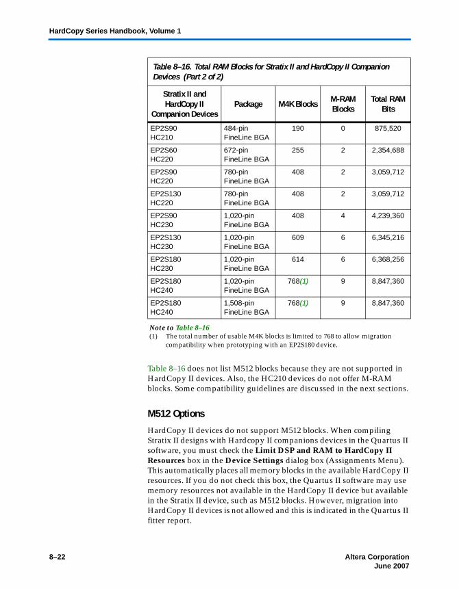
8–22 Altera CorporationJune 2007
HardCopy Series Handbook, Volume 1
Table 8–16 does not list M512 blocks because they are not supported in HardCopy II devices. Also, the HC210 devices do not offer M-RAM blocks. Some compatibility guidelines are discussed in the next sections.
M512 Options
HardCopy II devices do not support M512 blocks. When compiling Stratix II designs with Hardcopy II companions devices in the Quartus II software, you must check the Limit DSP and RAM to HardCopy II Resources box in the Device Settings dialog box (Assignments Menu). This automatically places all memory blocks in the available HardCopy II resources. If you do not check this box, the Quartus II software may use memory resources not available in the HardCopy II device but available in the Stratix II device, such as M512 blocks. However, migration into HardCopy II devices is not allowed and this is indicated in the Quartus II fitter report.
EP2S90HC210
484-pin FineLine BGA
190 0 875,520
EP2S60HC220
672-pin FineLine BGA
255 2 2,354,688
EP2S90HC220
780-pin FineLine BGA
408 2 3,059,712
EP2S130HC220
780-pin FineLine BGA
408 2 3,059,712
EP2S90HC230
1,020-pin FineLine BGA
408 4 4,239,360
EP2S130HC230
1,020-pin FineLine BGA
609 6 6,345,216
EP2S180HC230
1,020-pin FineLine BGA
614 6 6,368,256
EP2S180HC240
1,020-pin FineLine BGA
768(1) 9 8,847,360
EP2S180HC240
1,508-pin FineLine BGA
768(1) 9 8,847,360
Note to Table 8–16(1) The total number of usable M4K blocks is limited to 768 to allow migration
compatibility when prototyping with an EP2S180 device.
Table 8–16. Total RAM Blocks for Stratix II and HardCopy II Companion Devices (Part 2 of 2)
Stratix II and HardCopy II
Companion DevicesPackage M4K Blocks M-RAM
BlocksTotal RAM
Bits

Altera Corporation 8–23June 2007 Preliminary
Stratix II and HardCopy II Companion Memory Blocks
Your HardCopy II design can use M4K memory blocks to implement memory designs instead of M512 blocks. Quartus II megafunctions offer various memory implementations that use M4K blocks. When using the Quartus II MegaWizard® Plug-In Manager to configure the megafunction, Altera recommends selecting the Auto option to allow the Quartus II software to determine how the design is implemented in the memory blocks (Figure 8–2). This allows the Quartus II software to optimize memory selection based on memory size and placement requirements into the available memory blocks of the selected HardCopy II and Stratix II companion pair.
Figure 8–2. Quartus II MegaFunction RAM selection
You can select logic cells in the megafunction to implement small-memory blocks in your design. This implements the memory design in Stratix II ALMs or HardCopy II HCells. However, there may be power and performance trade-offs when choosing between an M4K or M-RAM block or using the ALMs (or HCells). HardCopy II devices power down unused M4K blocks, M-RAM blocks, and HCells.
1 Implementing memory blocks using logic cells, as seen in Figure 8–2, allows you to select a memory implementation functionally equivalent to M512 blocks or a non-equivalent option to save resources. Altera recommends setting the option to a functionally equivalent version with the M512 blocks.
For very small memory implementations such as a 8 × 16 single port RAM, the M4K or M-RAM blocks will be under-utilized, and may be less power efficient than a small number of HCells. If you select the logic cell option, only a fraction of ALMs are required in the Stratix II device, which translates into a small number HCells used in the HardCopy II device. However, when performance is a key factor, or your design requires ALMs to implement other logic, it may be more efficient to use M4K blocks. Altera recommends using the Quartus II software to analyze performance trade-offs between the given options.

8–24 Altera CorporationJune 2007
HardCopy Series Handbook, Volume 1
M4K Utilization
HardCopy II M4K block functionality is similar to Stratix II M4K blocks. You cannot pre-load HardCopy II M4K blocks with a memory initialization file (.mif) when used as RAM. Also, unlike Stratix II devices, the HardCopy II M4K RAM contents and their output registers are unknown after power up. However, if the HardCopy II M4K block is designated as ROM, it powers up with the ROM contents. When designing M4K blocks as RAM, Altera recommends writing to the block before reading from it to avoid reading unknown initial power-up data conditions. One advantage over Stratix II RAM blocks is unused M4K blocks are disconnected from the power rails, optimizing overall power consumption.
M-RAM Compatibility
HardCopy II M-RAM blocks share the same functionality as Stratix II M-RAM blocks. One key feature with HardCopy II M-RAM blocks is power optimization when the M-RAM block is not used. Unused M-RAM blocks are disconnected from the power rails, optimizing overall power consumption.
1 Some Stratix II devices (engineering sample devices and Revision A production devices) have M-RAM functionality that differs slightly from current Stratix II production devices. HardCopy II M-RAM functionality only matches that of current Stratix II devices. Hence, in order to maintain proper compatibility, compiling only for current production Stratix II devices is supported. More information on the Stratix II M-RAM errata can be found in the Stratix II FPGA Family Errata Sheet available on the Altera website (www.altera.com).

Altera Corporation 8–25June 2007 Preliminary
Stratix II and HardCopy II Companion Memory Blocks
Table 8–17 lists the M4K and M-RAM block supported features. This information can also be found in the HardCopy II Description, Architecture, and Features chapter of the HardCopy Series Handbook.
Table 8–17. HardCopy II Embedded Memory Features (Part 1 of 2)
Feature M4K Blocks M-RAM Blocks
Total RAM bits (including parity bits)
4,608 589,824
Configurations 4K × 12K × 21K × 4512 × 8512 × 9
256 × 16256 × 18128 × 32128 × 36
64K × 864K × 9
32K × 1632K × 1816K × 3216K × 368K × 648K × 72
4K × 1284K × 144
Parity bits v v
Byte enable v v
Pack mode v v
Address clock enable v v
Single-port memory v v
Simple dual-port memory v v
True dual-port memory v v
Embedded shift register v —
ROM v —
FIFO buffer v v
Simple dual-port mixed width support v v
True dual-port mixed width support v v
Memory initialization file (.mif) (1) —
Mixed-clock mode v v
Power-up condition Outputs unknown Outputs unknown
Register clears Output registers only Output registers only
Same-port read-during-write New data available at positive clock edge
New data available at positive clock edge

8–26 Altera CorporationJune 2007
HardCopy Series Handbook, Volume 1
PLL Planning and Utilization
Stratix II devices support enhanced PLLs and fast PLLs. HardCopy II devices also support enhanced PLLs and fast PLLs, but with two variations:
■ HardCopy II devices have a different number of PLLs than Stratix II devices.
■ HardCopy II devices may support fewer I/O standards for clock inputs and outputs. This is explained in the I/O standards support section later in this chapter.
Table 8–18 shows which PLLs each HardCopy II and Stratix II device supports. The Stratix II reference columns are divided based on package, not density. Figures 8–3 to 8–5 show PLL number designations. The Stratix II devices support 6 or 12 PLLs depending on the package offering, and not the device density. The HardCopy II PLLs are not removed symmetrically from all four sides. In general, fast PLLs are removed from sides that do not support high speed IOEs since the primary use of the fast PLL on the sides is for high speed I/O interface functions.
Mixed-port read-during-write Outputs set to unknown or old data
Unknown output
Power down of unused RAM blocks (2) v v
Notes to Table 8–17:(1) Stratix II M4K blocks support .mif file loading. (2) Stratix II memory blocks remain powered up even when not used.
Table 8–17. HardCopy II Embedded Memory Features (Part 2 of 2)
Feature M4K Blocks M-RAM Blocks
Table 8–18. Stratix II / HardCopy II Companion Device PLL Availability Guide (Part 1 of 2)
Stratix II and HardCopy II Companion
Devices
Package
Fast PLLs Enhanced PLLs
1 2 3 4 7 8 9 10 5 6 11 12
EP2S30HC210 (1)
484-pin FineLine BGAv v v v
EP2S60HC210 (1)
484-pin FineLine BGAv v v v
EP2S90HC210 (1)
484-pin FineLine BGA v v v v
EP2S60HC220 (1)
672-pin FineLine BGAv v v v

Altera Corporation 8–27June 2007 Preliminary
PLL Planning and Utilization
HardCopy II PLLs are functionally identical to the Stratix II PLLs. The HardCopy II enhanced and fast PLLs support reconfiguration and are also reconfigurable for bandwidth and phase shift.
Figures 8–3 to 8–5 show the PLL locations for each HardCopy II device.
For HC210 and HC220 devices, fast PLLs 1 and 2 are located in the logic array of the device and enhanced PLLs 5 and 6 are located in the periphery next to the device’s top and bottom I/O banks.
EP2S90HC220 (1)
780-pin FineLine BGA v v v v
EP2S130HC220 (1)
780-pin FineLine BGA v v v v
EP2S90HC230 (2)
1,020-pin FineLine BGAv v v v v v v v
EP2S130HC230 (2)
1,020-pin FineLine BGAv v v v v v v v
EP2S180HC230 (2)
1,020-pin FineLine BGAv v v v v v v v
EP2S180HC240
1,020-pin FineLine BGAv v v v v v v v v v v v
EP2S180HC240
1,508-pin FineLine BGAv v v v v v v v v v v v
Notes to Table 8–18:(1) HC210 and HC220 devices do not support fast PLLs 3, 4, 9, and 10, unlike Stratix II devices.(2) HC230 devices do not support fast PLLs 3 and 4, unlike Stratix II devices.
Table 8–18. Stratix II / HardCopy II Companion Device PLL Availability Guide (Part 2 of 2)
Stratix II and HardCopy II Companion
Devices
Package
Fast PLLs Enhanced PLLs
1 2 3 4 7 8 9 10 5 6 11 12

8–28 Altera CorporationJune 2007
HardCopy Series Handbook, Volume 1
Figure 8–3. HC210 and HC220 PLL Locations
HC230 device fast PLLs 1, 2, 7, and 8 are located in the logic array, next to the device’s left high-speed IOEs. HC230 device enhanced PLLs 5, 6, 11, and 12 are also located in the logic array, next to the top and bottom memory interface IOEs.
FPLL10CLK
FPLL9CLK
CLK[8..11]
FPLL7CLK
FPLL8CLK
CLK[3..0]
CLK[7..4]
CLK[15..12]
Bank 4Memory Interface IOEsPLL 5
Bank 9
Bank 7General Purpose IOEs
Bank 8General Purpose IOEs
PLL 6
Bank 10
Bank 3Memory Interface IOEs
Bank 2High-Speed IOEs
Bank 1High-Speed IOEs
Bank 5General-Purpose IOEs
Bank 6General-Purpose IOEs
PLL 1
PLL 2

Altera Corporation 8–29June 2007 Preliminary
PLL Planning and Utilization
Figure 8–4. HC230 PLL Locations
HC240 device fast PLLs 1, 2, 7, and 8 are located in the logic array, next to the left high speed IOEs of the device. HC240 device fast PLLs 3, 4, 9, and 10 are located in the logic array, next to the right high speed IOEs. HC240 device enhanced PLLs 5, 6, 11, and 12 are located in the logic array, next to the top and bottom memory interface IOEs.
FPLL10CLK
FPLL9CLK
CLK[8..11]
FPLL7CLK
FPLL8CLK
CLK[3..0]
CLK[7..4]
CLK[15..12]
Bank 4Memory Interface IOEs
Bank 7Memory Interface IOEs
Bank 8Memory Interface IOEs
Bank 3Memory Interface IOEs
Bank 2High-Speed IOEs
Bank 1High-Speed IOEs
Bank 5General-Purpose IOEs
Bank 6General-Purpose IOEs
PLL 1
PLL 2
PLL 7
PLL 8
PLL 5PLL 11
Bank 11 Bank 9
PLL 6PLL 12
Bank 12 Bank 10

8–30 Altera CorporationJune 2007
HardCopy Series Handbook, Volume 1
Figure 8–5. HC240 PLL Locations
Global and Local Signals
HardCopy II devices have 16 clock pins (CLK[15..0]) to drive either the global or local clock networks. Four clock pins drive each side of the device. This is similar to Stratix II devices; therefore, there are no limitations when compiling designs for Stratix II devices and HardCopy II companion devices.
Internal logic and enhanced and fast PLL outputs can also drive the global and regional clock networks. Each global and regional clock network has a clock control block, which controls the selection of the clock source and allows you to dynamically enable or disable the clock network to reduce power consumption.
FPLL10CLK
FPLL9CLK
CLK[8..11]
FPLL7CLK
FPLL8CLK
CLK[3..0]
Bank 4Memory Interface IOEs
Bank 7Memory Interface IOEs
Bank 8Memory Interface IOEs
Bank 3Memory Interface IOEs
Bank 2High-Speed IOEs
Bank 1High-Speed IOEs
Bank 5High-Speed IOEs
Bank 6High-Speed IOEs
PLL 1
PLL 2
PLL 4
PLL 3
PLL 10
PLL 9
PLL 7
PLL 8
PLL 5PLL 11
Bank 11 Bank 9
PLL 6PLL 12
Bank 12 Bank 10
CLK[7..4]
CLK[15..12]
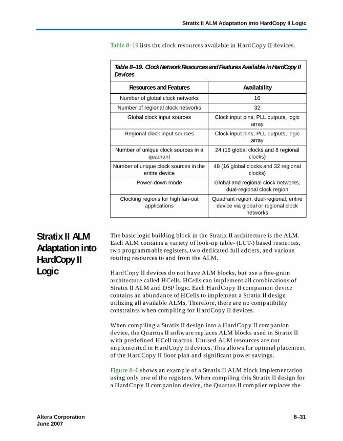
Altera Corporation 8–31June 2007 Preliminary
Stratix II ALM Adaptation into HardCopy II Logic
Table 8–19 lists the clock resources available in HardCopy II devices.
Stratix II ALM Adaptation into HardCopy II Logic
The basic logic building block in the Stratix II architecture is the ALM. Each ALM contains a variety of look-up table- (LUT-) based resources, two programmable registers, two dedicated full adders, and various routing resources to and from the ALM.
HardCopy II devices do not have ALM blocks, but use a fine-grain architecture called HCells. HCells can implement all combinations of Stratix II ALM and DSP logic. Each HardCopy II companion device contains an abundance of HCells to implement a Stratix II design utilizing all available ALMs. Therefore, there are no compatibility constraints when compiling for HardCopy II devices.
When compiling a Stratix II design into a HardCopy II companion device, the Quartus II software replaces ALM blocks used in Stratix II with predefined HCell macros. Unused ALM resources are not implemented in HardCopy II devices. This allows for optimal placement of the HardCopy II floor plan and significant power savings.
Figure 8–6 shows an example of a Stratix II ALM block implementation using only one of the registers. When compiling this Stratix II design for a HardCopy II companion device, the Quartus II compiler replaces the
Table 8–19. Clock Network Resources and Features Available in HardCopy II Devices
Resources and Features Availability
Number of global clock networks 16
Number of regional clock networks 32
Global clock input sources Clock input pins, PLL outputs, logic array
Regional clock input sources Clock input pins, PLL outputs, logic array
Number of unique clock sources in a quadrant
24 (16 global clocks and 8 regional clocks)
Number of unique clock sources in the entire device
48 (16 global clocks and 32 regional clocks)
Power-down mode Global and regional clock networks, dual-regional clock region
Clocking regions for high fan-out applications
Quadrant region, dual-regional, entire device via global or regional clock
networks

8–32 Altera CorporationJune 2007
HardCopy Series Handbook, Volume 1
ALM block with a predetermined HCell macro that implements a register from its HardCopy II library of HCell macros. This macro entry has predetermined timing.
Figure 8–6. Stratix II ALM Simple Registered Input and Output
Figure 8–7 shows a HardCopy II ALM register implementation showing Clock, Data In, and Data Out originating from a small cluster of HCells. Unused HCells are reserved for other logic implementation or powered down.
Figure 8–7. HardCopy II Unused HCells
PRN
reg0
D Qadder0
adder1
CombinationalLogic
dataf0
datae0
dataa
datab
datac
datad
datae1
dataf1
PRN
reg1
D Q
shared_arith_out
carry_out
reg_chain_out
reg_chain_in
carry_in
shared_arith_in
To General orLocal Routing
To General orLocal Routing
To General orLocal Routing
To General orLocal Routing

Altera Corporation 8–33June 2007 Preliminary
HardCopy II DSP Implementation from Stratix II DSP Blocks
HardCopy II DSP Implementation from Stratix II DSP Blocks
Stratix II FPGAs have dedicated DSP blocks to implement various DSP functions. Stratix II DSP blocks consist of multipliers, an adder/subtractor/accumulator and a summation block, input and output interfaces, and input and output registers. The Quartus II software implements DSP functions in HardCopy II devices with HCells using predetermined logic implementations from its library of HCell macros, all of which have predetermined timing.
DSP blocks that are not used in the Stratix II design are not implemented in Hardcopy II devices. This preserves the HardCopy II logic for other implementations, saving resources and power. Furthermore, the HardCopy II DSP block placement can be optimized to meet the timing constraint requirements placed on the HardCopy II designs.
The HardCopy II DSP implementation is functionally equivalent to Stratix II DSP blocks and all features are supported except for dynamic-mode switching. You can set up Stratix II DSP blocks to dynamically switch between the following three modes:
■ Up to four 18-bit independent multipliers■ Up to two 18-bit multiplier-accumulators ■ One 36-bit multiplier
HardCopy II DSP implementation does not support dynamic switching. If this feature is used, the Quartus II software flags the DSP implementation and does not allow you to migrate the design. The fitter reports that all HardCopy II devices are not compatible with the design. To migrate your Stratix II design to a HardCopy II companion device, disable dynamic switching in the DSP blocks.
The total number of DSP blocks is dependent on the Stratix II device selected. HardCopy II devices will match the available DSP block resources in the Stratix II device. Table 8–20 lists available DSP implementations based on the selected Stratix II device.
Table 8–20. DSP Multiplier Availability for Stratix II and HardCopy II Companion Devices (Part 1 of 2)
Stratix II Device
HC210 HC220 HC230 HC240
9 × 9 18 × 18 36 × 36 9 × 9 18 × 18 36 × 36 9 × 9 18 × 18 36 × 36 9 × 9 18 × 18 36 × 36
EP2S30 128 64 16
EP2S60 288 144 36 288 144 36
EP2S90 (1)
384 192 48 384 192 48 384 192 48
EP2S130 (1)
504 252 63 504 252 63

8–34 Altera CorporationJune 2007
HardCopy Series Handbook, Volume 1
Figure 8–8 shows an example of a Stratix II DSP block that uses only 1 of 8 available 9 × 9 multiplier blocks and an accumulator block to implement an 8 × 8 bit multiplication function with clock latency. When this DSP block is implemented in the HardCopy II design, the Quartus II Compiler chooses the appropriate entry from the macro library to implement the 9 × 9 multiplier and accumulator block which results in an optimized logic utilization and placement flexibility.
Figure 8–8. HardCopy II Floorplan of 8 × 8 DSP Block
EP2S180 (1)
768 384 96 768 384 96
Note to Table 8–20:(1) If these Stratix II devices are selected with smaller HardCopy II companion devices, all Stratix II DSP resources may
not be available if all the Stratix II ALM blocks are used and fully utilized. Quartus II will determine available resources for DSP and ALM implementation when compiling with HardCopy II devices.
Table 8–20. DSP Multiplier Availability for Stratix II and HardCopy II Companion Devices (Part 2 of 2)
Stratix II Device
HC210 HC220 HC230 HC240
9 × 9 18 × 18 36 × 36 9 × 9 18 × 18 36 × 36 9 × 9 18 × 18 36 × 36 9 × 9 18 × 18 36 × 36

Altera Corporation 8–35June 2007 Preliminary
JTAG BST and Extended Functions
Figure 8–9 shows Quartus II floor plans of a Stratix II DSP block on the left and a HardCopy II DSP implementation on the right, both configured with an 18 × 18 multiply with accumulate function. In the HardCopy II implementation, the Quartus II software selected the appropriate DSP logic implementation from the macro library which results in an optimal utilization of the HardCopy II device’s HCells. The unused sections of the Stratix II DSP block remain powered up, but these are not implemented in the HardCopy II device. Unused logic in HardCopy II devices are powered down.
Figure 8–9. HardCopy II Floorplan of 18 × 18 DSP Block
JTAG BST and Extended Functions
HardCopy II devices support the same boundary-scan test (BST) functionality as the Stratix II devices. However, since HardCopy II devices are mask-programmed, no reconfiguration is possible. Therefore, HardCopy II devices do not support instructions to reconfigure the device through the JTAG pins. For a list of supported features and instruction codes, refer to the Boundary-Scan Support chapter of the HardCopy Series Handbook.
One Stratix II feature utilizing JTAG pins is the Signal Tap II embedded logic analyzer (ELA). HardCopy II devices support the JTAG ELA feature. However, designing with this feature will use additional resources and may reduce peak performance in Stratix II and

8–36 Altera CorporationJune 2007
HardCopy Series Handbook, Volume 1
HardCopy II devices. Unlike Stratix II devices, where this feature can be eliminated prior to compiling a final version of the design, HardCopy II devices are masked programmed and this feature will remain permanent in the HardCopy II device. Therefore, if the design requires optimal performance and resource utilization, Altera recommends using this feature on the Stratix II prototype device, but eliminating it prior to recompiling the design for a HardCopy II device.
Power Up and Configuration Compatibility
When designing a board with a Stratix II prototype device and its companion HardCopy II device, most configuration pins required by the Stratix II device are not required by the HardCopy II device. To maximize I/O pin counts with HardCopy II device utilization, Altera recommends minimizing power up and configuration pins that will not carry over from a Stratix II device into a HardCopy II device. Table 8–21 lists the dedicated and optional configuration pins that a Stratix II device can use and if their optional functionality is used on a HardCopy II device.
If the HardCopy II device can use the pin’s optional function found in Stratix II devices, the Quartus II software allows you to set these pins as dual purpose pins. As dual purpose pins, they have I/O functionality after power up, reconfiguration and initialization. These pins will only switch to their I/O designation when the device enters user mode (when INIT_DONE is asserted). The design may require that some signals be present when the device transitions into user mode, so you should not use dual purpose pins because it may result in unstable operation after power up for both the HardCopy II and the Stratix II devices.
Table 8–21. Power Up and Configuration Pin Compatibility (Part 1 of 3)
Stratix II Pin Name
I/O Bank
HardCopy II Use
Main Function Optional Function Main Function Optional
Function
MSEL3 B4
MSEL2 B4
MSEL1 B4
MSEL0 B4
VCCSEL B8 v v
nCONFIG B8 v v
nSTATUS B3 v v
CONF_DONE B3 v v
nCE B3 v v

Altera Corporation 8–37June 2007 Preliminary
Power Up and Configuration Compatibility
nCEO B7 v v
PORSEL B7 v v
nIO_PULLUP B7 v v
PLL_ENA B7 v v
I/O pin CLKUSR B8 v
I/O pin DEV_OE B8 v v
I/O pin DEV_CLRn B8 v v
I/O pin INIT_DONE B3 v v
DCLK B3 v
I/O pin DATA0 B3 v
I/O pin DATA1 B3 v
I/O pin DATA2 B3 v
I/O pin DATA3 B3 v
I/O pin DATA4 B3 v
I/O pin DATA5 B3 v
I/O pin DATA6 B3 v
I/O pin DATA7 B3 v
I/O pin RDYnBSY B3 v
I/O pin CRC_ERROR B3 v
I/O pin CS B8 v
I/O pin nCS B8 v
I/O pin nRS B8 v
I/O pin nWS B8 v
I/O pin RUnLU B8 v
I/O pin PGM2 B3 v
I/O pin PGM1 B3 v
I/O pin PGM0 B3 v
Table 8–21. Power Up and Configuration Pin Compatibility (Part 2 of 3)
Stratix II Pin Name
I/O Bank
HardCopy II Use
Main Function Optional Function Main Function Optional
Function

8–38 Altera CorporationJune 2007
HardCopy Series Handbook, Volume 1
Most optional configuration pins listed in Table 8–21 support the various configuration schemes available in Stratix II FPGAs. Parallel programming and remote update configuration modes utilize most of the pins in Table 8–21. HardCopy II devices are not configurable and do not support the Configuration Emulation mode. Therefore, Altera recommends that you minimize the configuration pin requirements of the Stratix II design; for example, by using the Passive Serial configuration mode.
If some of these dual-purpose pins are needed to configure the Stratix II FPGA, but will be unused after configuration, these pins will be completely unused on the HardCopy II device. Therefore, when migrating from the Stratix II device to the HardCopy II device, care must be taken when designing these pins on board. The removal of the Stratix II device and its corresponding configuration device may leave these pins floating on the HardCopy II device if such pins are assigned as inputs by the user, without any external means of driving them to a stable level. When selecting a Stratix II device and its device options, consider the after-configuration requirements of these pins and set them appropriately in the Quartus II software (Figure 8–10).
I/O pin ASDO B3 v
I/O pin nCSO B3 v
Table 8–21. Power Up and Configuration Pin Compatibility (Part 3 of 3)
Stratix II Pin Name
I/O Bank
HardCopy II Use
Main Function Optional Function Main Function Optional
Function

Altera Corporation 8–39June 2007 Preliminary
Conclusion
Figure 8–10. Device and Pin Options
f For more information about HardCopy II power-up modes, refer to the Power-Up Modes and Configuration Emulation in HardCopy Series Devices chapter of the HardCopy Series Handbook.
Conclusion HardCopy II devices provide a seamless migration path for Stratix II devices and supports the PLL, memory, logic, and I/O features offered on a Stratix II device. The HardCopy II device architecture also allows you to use a wide range of Stratix II devices for prototyping. HardCopy II devices offer pin-to-pin compatibility with Stratix II FPGAs, making HardCopy II devices drop-in replacements on systems designed with the Quartus II software and using Stratix II and HardCopy II companion devices. Use the Quartus II software to compile designs and determine available resources to guarantee fit and feature compatibility for Stratix II and HardCopy II companion devices.
8–40 Altera CorporationJune 2007
HardCopy Series Handbook, Volume 1
More Information
For more information on migrating Stratix II designs to HardCopy II devices, Refer to the following sources:
■ HardCopy II Device Family Data Sheet in the HardCopy Series Handbook■ Quartus II Support for HardCopy II Devices■ Power-Up Modes and Configuration Emulation in HardCopy Series
Devices chapter in the HardCopy Series Handbook
Document Revision History
Table 8–22 shows the revision history for this chapter.
Table 8–22. Document Revision History
Date and Document Version Changes Made Summary of Changes
June 2007 v1.3 Changed “8K x 64” to “16K x 36” in Table 8–17.
Completed typographical updates.
December 2006 v1.2
Added revision history.
March 2006 Formerly chapter 19; no content change.
October 2005 v1.1 Minor edits
May 2005v1.0
Added document to the HardCopy Series Handbook.