silicon photomultiplier readout electronics for the gluex tagger microscope hall d electronics...
Post on 21-Dec-2015
218 views
TRANSCRIPT
Silicon Photomultiplier Silicon Photomultiplier Readout ElectronicsReadout Electronics
for the GlueXfor the GlueX
Tagger MicroscopeTagger Microscope
Hall D Electronics Meeting, Newport News, Oct. 23-24, 2007
Richard Jones, Igor Senderovich and Brendan KruegerRichard Jones, Igor Senderovich and Brendan KruegerUniversity of ConnecticutUniversity of Connecticut
Hall D Electronics Meeting, Newport News, Oct. 23-24, 2007Hall D Electronics Meeting, Newport News, Oct. 23-24, 2007 22
OutlineOutline
1.1. Detector overview and requirementsDetector overview and requirements
2.2. Silicon photomultipliersSilicon photomultipliers
3.3. Signal pathwaysSignal pathways
4.4. Detector electronics requirementsDetector electronics requirements
5.5. Conceptual designConceptual design
6.6. ImplementationImplementation
7.7. Project status and plansProject status and plans
Hall D Electronics Meeting, Newport News, Oct. 23-24, 2007Hall D Electronics Meeting, Newport News, Oct. 23-24, 2007 33
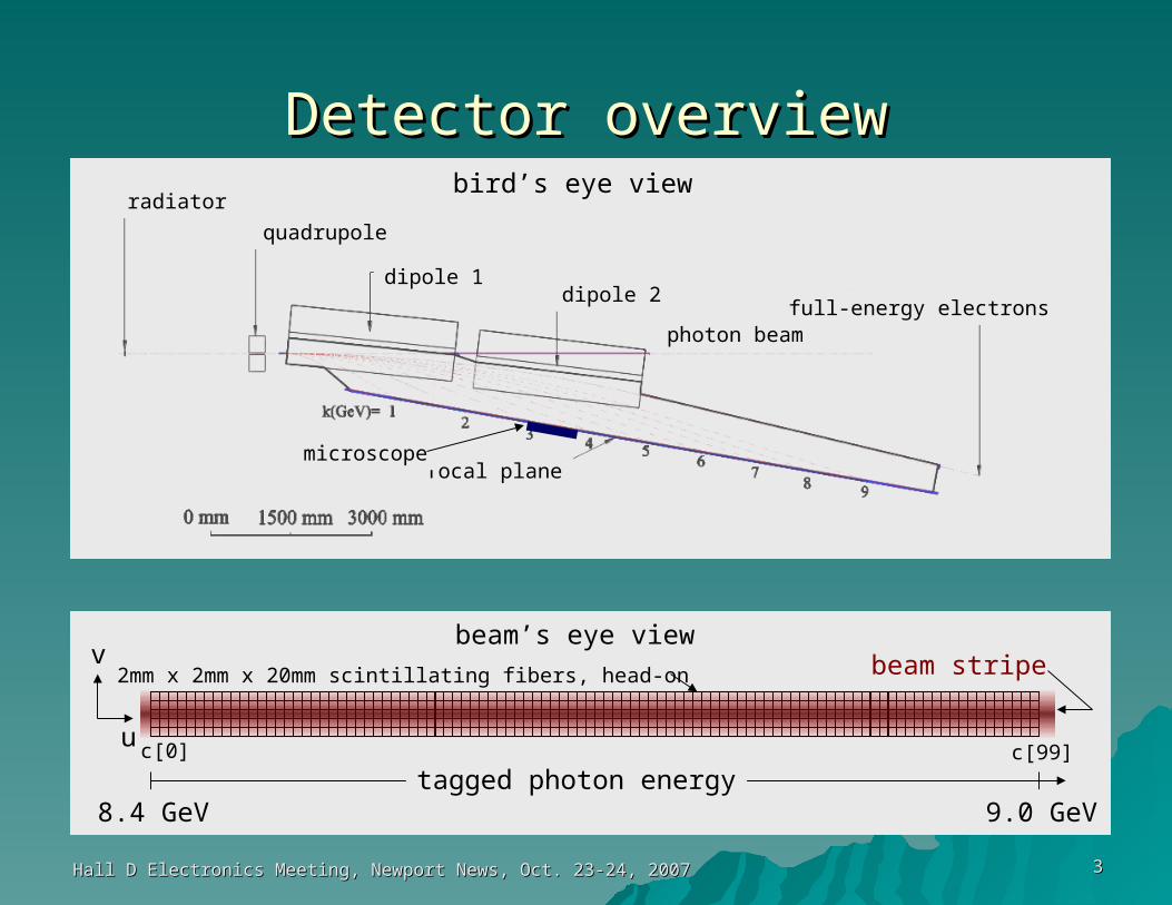
Detector overviewDetector overviewradiator
quadrupole
dipole 1dipole 2
photon beamfull-energy electrons
focal planemicroscope
bird’s eye view
beam’s eye view
u
v
tagged photon energy9.0 GeV8.4 GeV
beam stripe2mm x 2mm x 20mm scintillating fibers, head-on
c[0] c[99]
Hall D Electronics Meeting, Newport News, Oct. 23-24, 2007Hall D Electronics Meeting, Newport News, Oct. 23-24, 2007 44
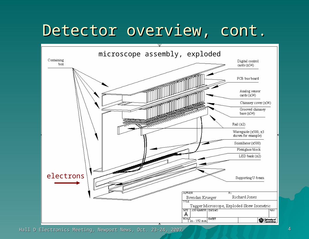
Detector overview, cont.Detector overview, cont.
electrons
microscope assembly, exploded
Hall D Electronics Meeting, Newport News, Oct. 23-24, 2007Hall D Electronics Meeting, Newport News, Oct. 23-24, 2007 55
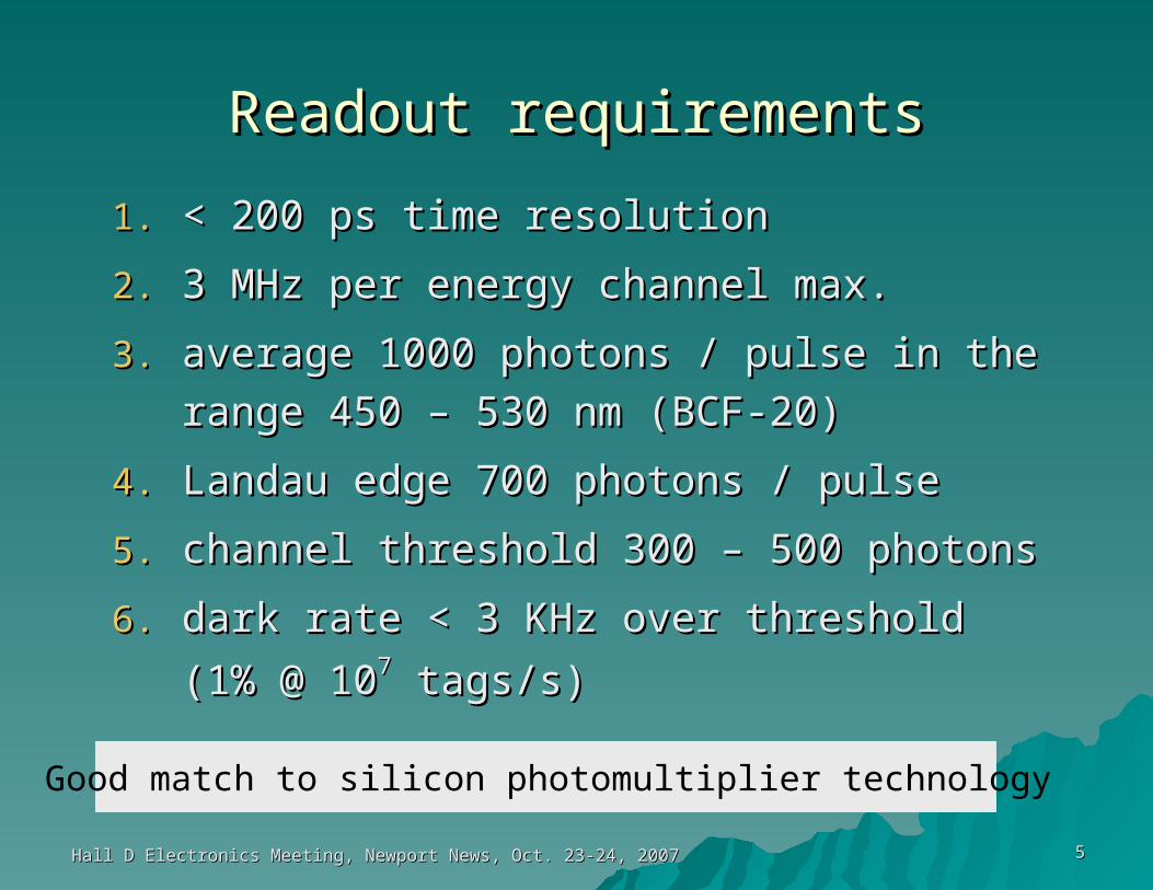
Readout requirementsReadout requirements
1.1. < 200 ps time resolution< 200 ps time resolution
2.2. 3 MHz per energy channel max.3 MHz per energy channel max.
3.3. average 1000 photons / pulse in the average 1000 photons / pulse in the
range 450 – 530 nm (BCF-20)range 450 – 530 nm (BCF-20)
4.4. Landau edge 700 photons / pulseLandau edge 700 photons / pulse
5.5. channel threshold 300 – 500 photonschannel threshold 300 – 500 photons
6.6. dark rate < 3 KHz over thresholddark rate < 3 KHz over threshold (1% (1%
@ 10@ 1077 tags/s) tags/s)
Good match to silicon photomultiplier technology
Hall D Electronics Meeting, Newport News, Oct. 23-24, 2007Hall D Electronics Meeting, Newport News, Oct. 23-24, 2007 66
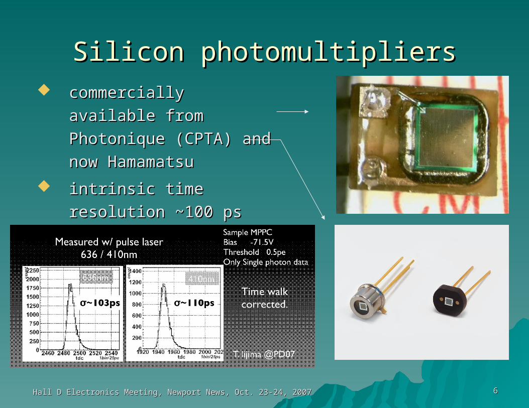
Silicon photomultipliersSilicon photomultipliers commercially available commercially available
from Photonique (CPTA) from Photonique (CPTA)
and now Hamamatsuand now Hamamatsu
intrinsic time resolution intrinsic time resolution
~100 ps for 1 p.e. pulse~100 ps for 1 p.e. pulse
Hall D Electronics Meeting, Newport News, Oct. 23-24, 2007Hall D Electronics Meeting, Newport News, Oct. 23-24, 2007 77
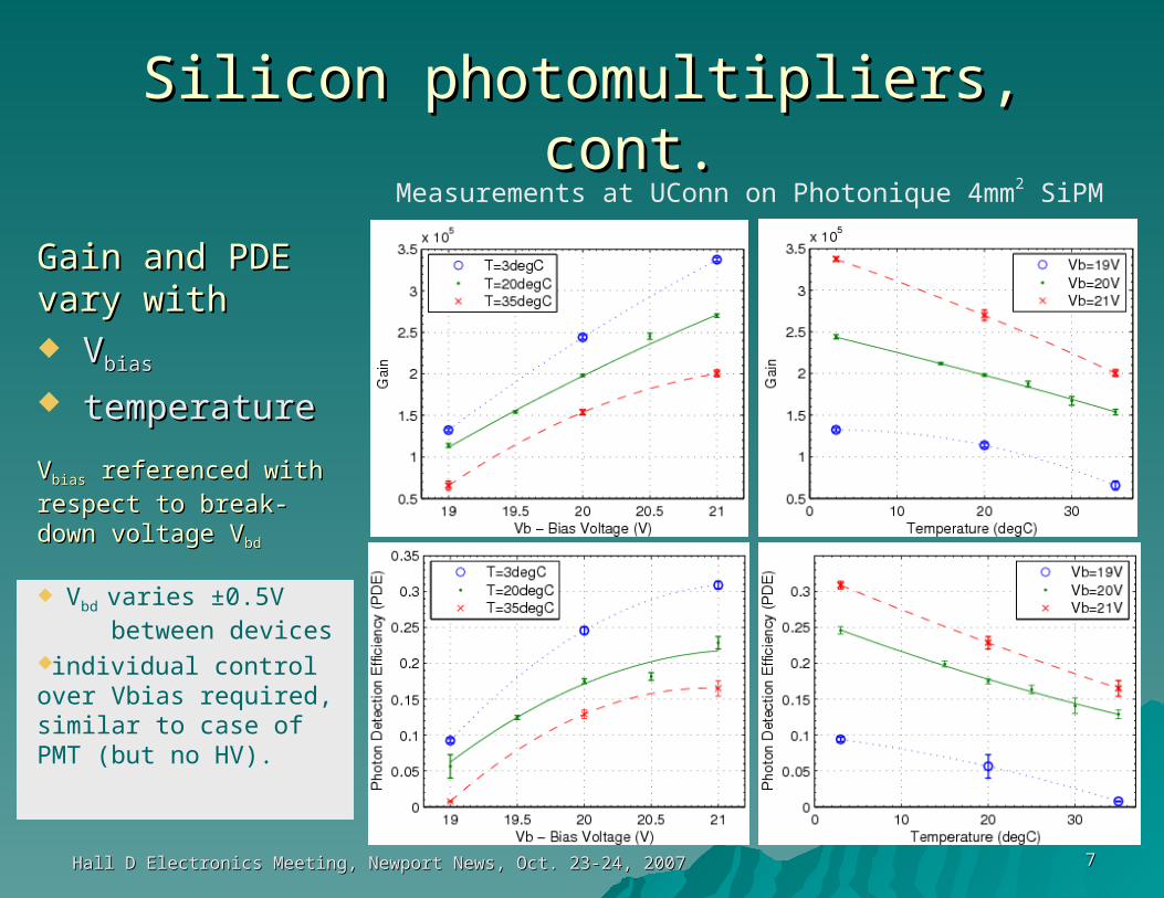
Silicon photomultipliers, cont.Silicon photomultipliers, cont.Measurements at UConn on Photonique 4mm2 SiPM
Gain and PDE Gain and PDE vary withvary with VVbiasbias
temperaturetemperature
VVbiasbias referenced with referenced with respect to break-respect to break-down voltage Vdown voltage Vbdbd
Vbd varies ±0.5V between devicesindividual control over Vbias required, similar to case of PMT (but no HV).

Hall D Electronics Meeting, Newport News, Oct. 23-24, 2007Hall D Electronics Meeting, Newport News, Oct. 23-24, 2007 88
Signal pathwaysSignal pathways
+
SiPMV
b[0]
E[0]SiPM
SiPMSiPM
SiPM
...
...
...V
b[4]
cfd
fadc[0]
f1tdc[0]
EnergyBins scint. clear
Fibers: Biasvoltages Detector DAQ Rack
+
SiPM
E[99]SiPM
SiPM
SiPM
SiPM
...
...
...V
b[499]
.
.
.
...
.
.
.
.
.
cfd
fadc[119]
f1tdc[119]
95 Echan @ 1 daqchan/Echan + 5 Echan @ 5 daqchan/Echan = 120 daqchan
Hall D Electronics Meeting, Newport News, Oct. 23-24, 2007Hall D Electronics Meeting, Newport News, Oct. 23-24, 2007 99
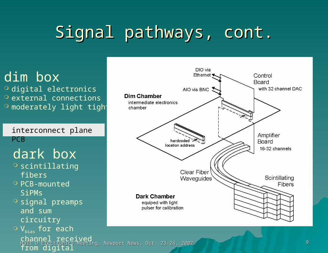
Signal pathways, cont.Signal pathways, cont.
dim box digital electronics external connections moderately light tight
dark box scintillating fibers PCB-mounted SiPMs signal preamps and
sum circuitry Vbias for each
channel received from digital board
interconnect plane PCB
Hall D Electronics Meeting, Newport News, Oct. 23-24, 2007Hall D Electronics Meeting, Newport News, Oct. 23-24, 2007 1010
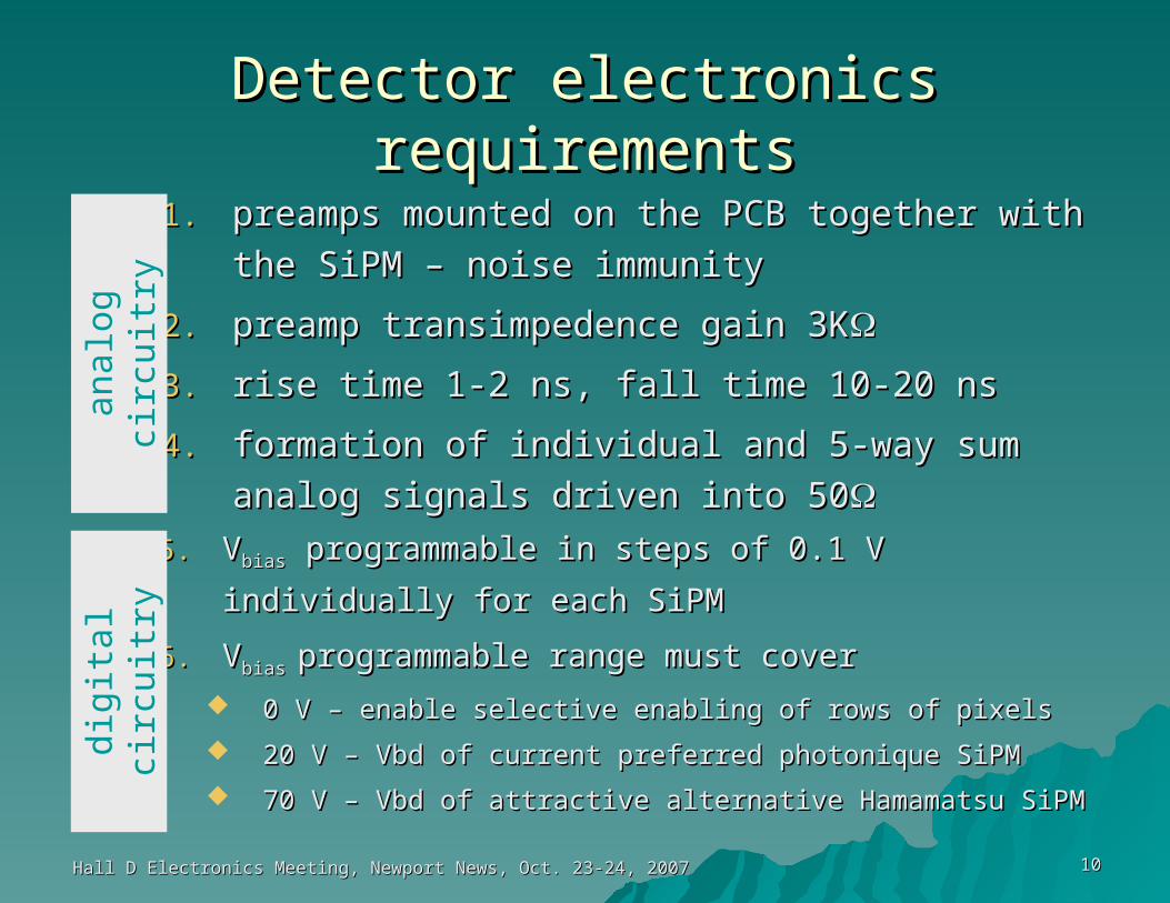
Detector electronics requirementsDetector electronics requirements
1.1. preamps mounted on the PCB together with the preamps mounted on the PCB together with the
SiPM – noise immunitySiPM – noise immunity
2.2. preamp transimpedence gain 3Kpreamp transimpedence gain 3K
3.3. rise time 1-2 ns, fall time 10-20 nsrise time 1-2 ns, fall time 10-20 ns
4.4. formation of individual and 5-way sum analog formation of individual and 5-way sum analog
signals driven into 50signals driven into 50
5.5. VVbiasbias programmable in steps of 0.1 V individually programmable in steps of 0.1 V individually
for each SiPMfor each SiPM
6.6. VVbias bias programmable range must coverprogrammable range must cover 0 V – enable selective enabling of rows of pixels 0 V – enable selective enabling of rows of pixels
20 V – Vbd of current preferred photonique SiPM20 V – Vbd of current preferred photonique SiPM
70 V – Vbd of attractive alternative Hamamatsu SiPM70 V – Vbd of attractive alternative Hamamatsu SiPM
an
alo
g c
ircu
itry
dig
ital ci
rcuit
ry
Hall D Electronics Meeting, Newport News, Oct. 23-24, 2007Hall D Electronics Meeting, Newport News, Oct. 23-24, 2007 1111
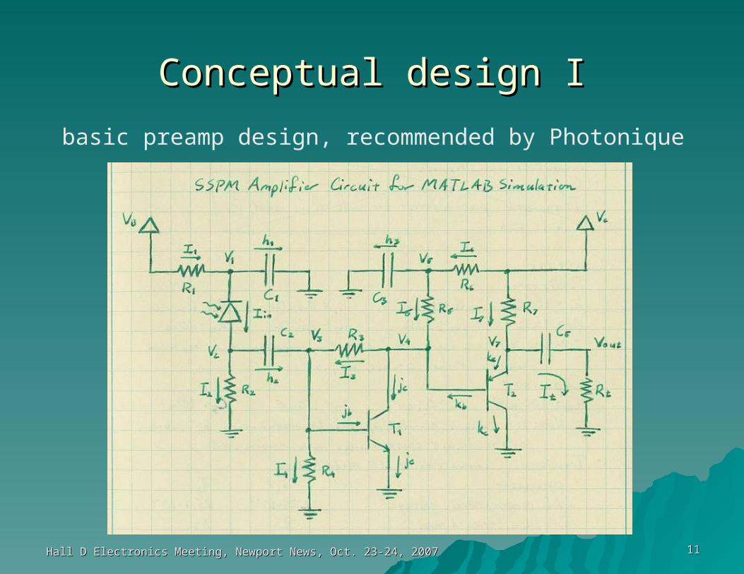
Conceptual design IConceptual design I
basic preamp design, recommended by Photonique
Hall D Electronics Meeting, Newport News, Oct. 23-24, 2007Hall D Electronics Meeting, Newport News, Oct. 23-24, 2007 1212
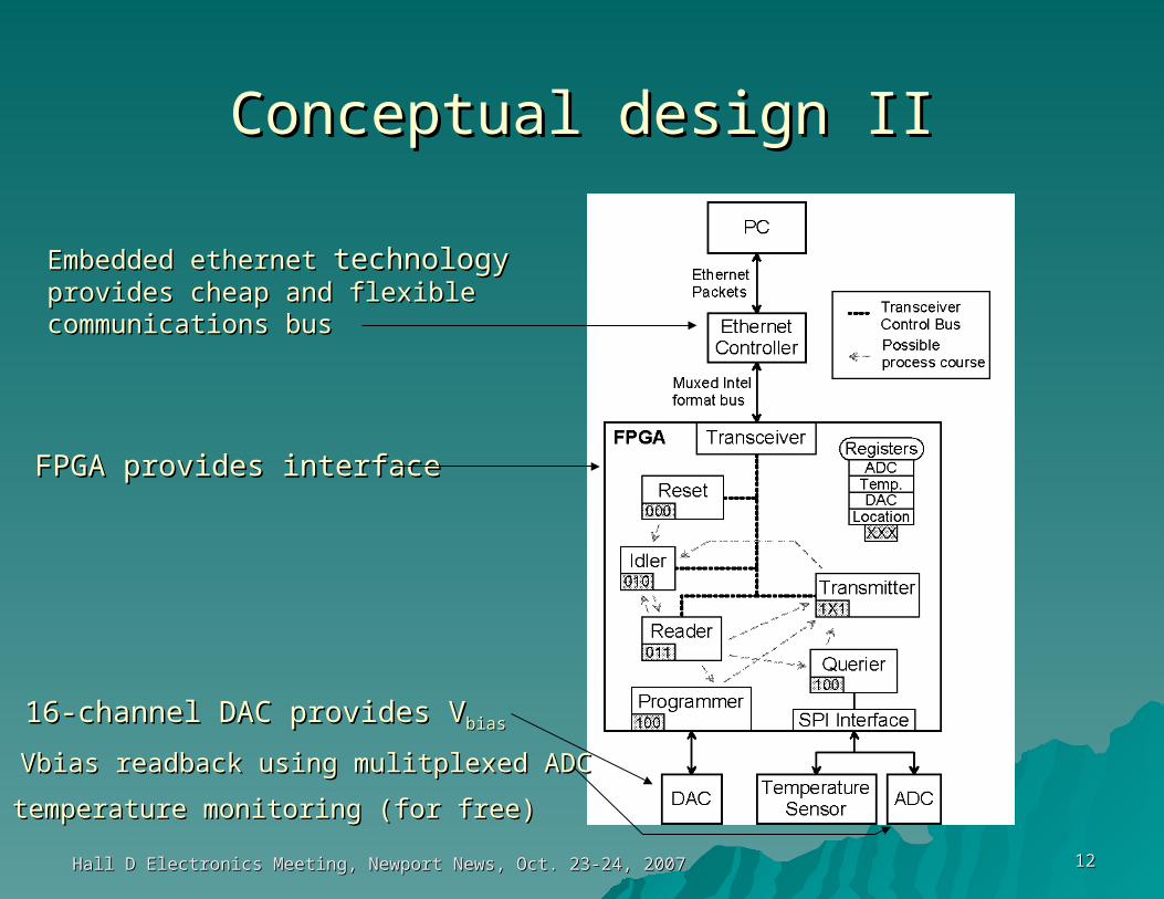
Conceptual design IIConceptual design II
16-channel DAC provides V16-channel DAC provides Vbiasbias
Vbias readback using mulitplexed ADCVbias readback using mulitplexed ADC
temperature monitoring (for free)temperature monitoring (for free)
FPGA provides interfaceFPGA provides interface
Embedded ethernet Embedded ethernet technologytechnologyprovides cheap and flexibleprovides cheap and flexiblecommunications buscommunications bus

Hall D Electronics Meeting, Newport News, Oct. 23-24, 2007Hall D Electronics Meeting, Newport News, Oct. 23-24, 2007 1313
ImplementationImplementation
1.1. Xilinx FPGAXilinx FPGA
2.2. external components modeled in VHDLexternal components modeled in VHDL
3.3. detailed simulation during and after detailed simulation during and after design using Xilinx development toolsdesign using Xilinx development tools
4.4. robust set of test sequences to exercise robust set of test sequences to exercise major functionsmajor functions
5.5. ethernet complexity handled by ethernet ethernet complexity handled by ethernet controller – only host bus side simulatedcontroller – only host bus side simulated
Hall D Electronics Meeting, Newport News, Oct. 23-24, 2007Hall D Electronics Meeting, Newport News, Oct. 23-24, 2007 1414
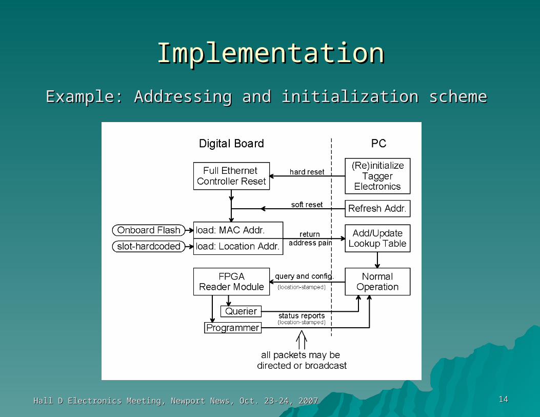
ImplementationImplementation
Example: Addressing and initialization schemeExample: Addressing and initialization scheme

Hall D Electronics Meeting, Newport News, Oct. 23-24, 2007Hall D Electronics Meeting, Newport News, Oct. 23-24, 2007 1515
Project status and plansProject status and plans
1.1. Project started by 1 undergraduate student Project started by 1 undergraduate student
summer 2007summer 2007
2.2. Taken over fall 2007 by graduate student Taken over fall 2007 by graduate student
3.3. VHDL design of digital side 70% finishedVHDL design of digital side 70% finished
4.4. Single channel of preamp passed tests on benchSingle channel of preamp passed tests on bench
5.5. PADS PCB layout software PADS licenced PADS PCB layout software PADS licenced
installed at Uconn for layoutinstalled at Uconn for layout
6.6. Design (analog+digital) expected to be ready for Design (analog+digital) expected to be ready for
prototyping summer 2008prototyping summer 2008