sima dezső architectural integration of cpus and gpus 2014 október version 1.1
TRANSCRIPT
Sima Dezső
Architectural integration of CPUs and GPUs
2014 Október
Version 1.1

Áttekintés
1. Introduction to architectural integration of the CPU and GPU•
2. AMD’s approach to support heterogeneous computing•
3. Intel’s approach to support heterogeneous computing•
2.1 Introduction to HSA•
3.1 Intel’s implementations of integrated graphics•
3.2 Intel’s first implementation of Shared Virtual Memory - The Core M processor
•
2.2 Key hardware enhancements needed to implement HSA•
2.3 AMD’s first implementation of HSA - Kaveri•
4. NVIDIA’s planned introduction of Unified Memory•
5. References•

1. Introduction to architectural integration of the CPU and GPU

1. Introduction to architectural integration of the CPU and GPU (1)
1. Introduction to architectural integration of the CPU and GPU
Heterogeneous processing
Aim of architectural integration of the CPU and GPU
Accelerated graphics processing
• Accelerating HPC by the GPU, i.e. by the large number of FP units available in a GPU.
• Accelerating graphics processing by the higher bandwidth of connecting the CPU and the GPU.• Cost reduction
Needs HLL support (CUDA, OPenCL)

Unified system memory(Shared memory)
(Unified Virtual Memory)(Unified Memory Architecture)
Implementation of the graphics memory
Discrete graphics memory
Implementation alternatives of graphics memory [1]
Implementation example
Typ. useGraphics cards On-die integrated graphics
1. Introduction to architectural integration of the CPU and GPU (2)

It eliminates the need for an extra graphics memory controller and bus but has the constraints of a reduced memory bandwidth.
Key benefit/drawback of the Unified system memory [1]
Unified system memory(Shared memory)
(Unified Virtual Memory)(Unified Memory Architecture)
Implementation of the graphics memory
Discrete graphics memory
Implementation example
1. Introduction to architectural integration of the CPU and GPU (3)

Address spaces for Discrete and Unified System Memory (USM) [2]
USMNo USM
1. Introduction to architectural integration of the CPU and GPU (4)

Main difficulty of heterogeneous computing
• GPUs operate from their own address spaces, thus without appropriate hardware and software support data to be processed by GPUs need to be loaded into their address space and the results need to be sent back to the host.
• Transferring data may be avoided with unified system memory and suitable software support (CUDA 4.0 or OpenCL 1.2 or higher) assuming appropriate hardware.
Then data transfer will be substituted by address mapping (called zero copy).
1. Introduction to architectural integration of the CPU and GPU (5)
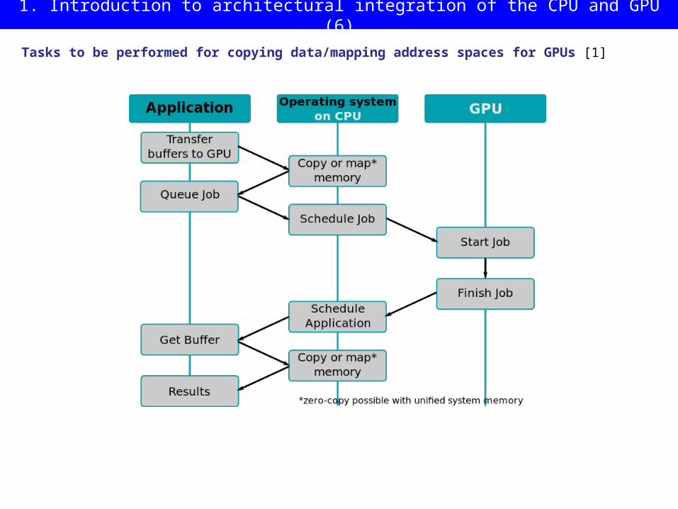
Tasks to be performed for copying data/mapping address spaces for GPUs [1]
1. Introduction to architectural integration of the CPU and GPU (6)
2. AMD’s approach to support heterogeneous computing

2.1 Introduction to HSA

2.1 Introduction to HSA (1)
2.1 Introduction to HSA (Heterogeneous System Architecture)
The notion of HSA [3]

Aim of HSA-1 [4]
2.1 Introduction to HSA (2)

Aim of HSA-2 [5]
2.1 Introduction to HSA (3)

The entire HSA solution stack [6]
HSAIL: HSA Intermediate Language
2.1 Introduction to HSA (4)

Establishment of the HAS Foundation
• In 6/2012 AMD, ARM, TI Qualcomm, Samsung and several other leading semiconductor firms established the Heterogeneous System Architecture (HSA) Foundation.
• It is a non-profit consortium that aims at defining and promoting open standards for heterogeneous computing.
2.1 Introduction to HSA (5)

2.2 Key hardware enhancements needed to implement HSA
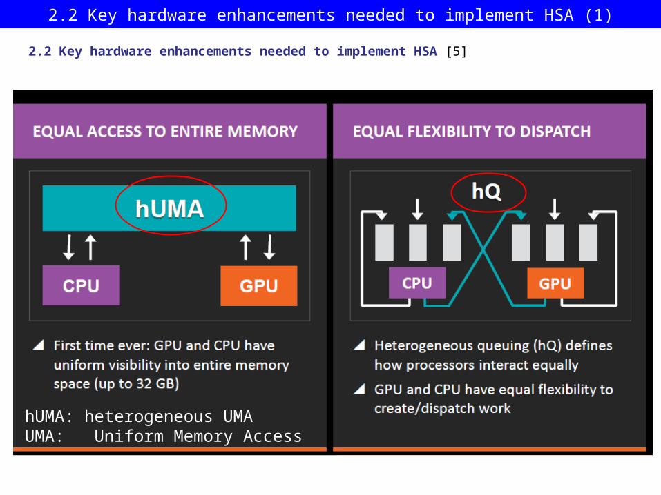
2.2 Key hardware enhancements needed to implement HSA [5]
2.2 Key hardware enhancements needed to implement HSA (1)
hUMA: heterogeneous UMA UMA: Uniform Memory Access

2.2.1 hUMA (Heterogeneous Uniform Memory Access)
2.2 Key hardware enhancements needed to implement HSA (2)

(Non-Uniform Memory Access)
(Uniform Memory Access)
(heterogeneous UMA)
The hUMA (heterogenous UMA) memory access scheme [3]
2.2 Key hardware enhancements needed to implement HSA (3)

GPU co-processing of data structures without hUMA [3]
2.2 Key hardware enhancements needed to implement HSA (4)

GPU co-processing of data structures with hUMA [3]
2.2 Key hardware enhancements needed to implement HSA (5)

The evolution path to HSA in AMD’s subsequent Family 15h based APU lines [7]
2.2 Key hardware enhancements needed to implement HSA (6)

Key requirements of hUMA-1 [3]
2.2 Key hardware enhancements needed to implement HSA (7)
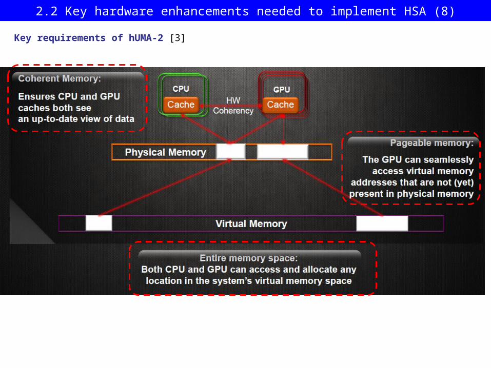
Key requirements of hUMA-2 [3]
2.2 Key hardware enhancements needed to implement HSA (8)

AMD Tech Day 2014 Jan
Hardware support of memory management in Kaveri [8]
2.2 Key hardware enhancements needed to implement HSA (9)

2.2.2 hQ (heterogeneous Queuing)
2.2 Key hardware enhancements needed to implement HSA (10)

Traditional management of application tasks queues [9]
2.2 Key hardware enhancements needed to implement HSA (11)

Application task management with heterogeneous queuing (hQ) [9]
2.2 Key hardware enhancements needed to implement HSA (12)

• Heterogeneous queuing (hQ) is symmetrical.
It allows both the CPU and the GPU to generate tasks for themselves and for each other.
• Work is specified in a standard packet format that will be supported by all HSA-compatible hardware, so there's no need for the software to use vendor-specific code.
• Applications can put packets directly into the task queues that will be accessed by the hardware.
• Each application can have multiple task queues, and a virtualization layer allows HSA hardware to see all the queues.
Main features of hQ [9]
2.2 Key hardware enhancements needed to implement HSA (13)

2.3 AMD’s first implementation of HSA - Kaveri

2.3 AMD’s first implementation of HSA – Kaveri (1)
2.3 AMD’s first implementation of HSA - Kaveri
AMD’s Kaveri
• Launched in 6/2014• Is based on the 3. version of the Bulldozer family, called Steamroller.• Aims at desktop PCs and laptops.

AMD’s Family 15h Steamroller-based Kaveri APU lines (based on [10])
F
u
s
i
o
n
Fam. 12h
K14
Fam. 14h
Fam. 12h
??40 nm
??Brazos(Desna)
2 Cores 1MBDX11 GPU Core
DDR3
1.G.Bobcat2. G.
2.3 AMD’s first implementation of HSA – Kaveri (2)

Die shot of Kaveri [8]
2.3 AMD’s first implementation of HSA – Kaveri (3)

Kaveri die layout [11]
2.3 AMD’s first implementation of HSA – Kaveri (4)

3. Intel’s approach to support heterogeneous computing

3.1 Intel’s implementations of integrated graphics

3.1 Intel’s implementations of integrated graphics (1)
3.1 Intel’s implementations of integrated graphics
Intel has a long history of integrated graphics, implemented first in the north bridge in the 8xx chipset (1999), as indicated below.
Implementation of integrated graphics
In the north bridge On the processor dieIn a multi-chip processor package on a separate die
Both the CPU and the GPU are on separate diesand are mounted into a single package
Implementations about1999 – 2009 such as
Intel’s 828xx chipset (1999)and subsequent implementations
P
South Bridge
Mem.NBIG
South Bridge
Mem.NB
PGPU CPU
Periph. Contr.
Mem.CPUGPUP
Intel’s Havendale (DT) andAuburndale (M)
(scheduled for 1H/2009 but cancelled)
Arrandale (DT, 1/2010) andClarkdale (M, 1/2010)
Intel’s Sandy Bridge (1/2011) andsubsequent processors
AMD’s Swift (scheduled for 2009but canceled)
AMD’s Bobcat-based APUs (M, 1/2011)Llano APUs (DT, 6/2011)
and subsequent processors

Unified Memory Architecture (UMA)
Some early graphics cards of other vendors and essentially all (in the north bridge) integrated graphics designs of Intel already made use of the UMA design as early as in the second half of the 1990s, as the next Figure shows for the integrated graphics of the Intel 810 chipset (1999).
Figure: The UMA design of an early (in the north bridge) integrated graphics [12]
The UMA design eliminates the need for an extra graphics memory controller and bus but has the constraints of a reduced memory bandwidth.
Key benefit/drawback of the UMA design
CPUGraphics/Memory
Controller
Gfx/MemoryArbiter
OptionalDisplayCache
System memory FB
DirectAGP
3.1 Intel’s implementations of integrated graphics (2)

Intel’s on-die integrated graphics designs
Subsequently, we discuss only those on-die integrated CPU-GPU solutions that support also HPC i.e. have OpenCL support, as follows.
Table: Intel’s processors with on-die integrated GPUs [13]
3.1 Intel’s implementations of integrated graphics (3)
OpenCL2.0
OpenCL1.2
OpenCL1.2
OpenCL1.2
NoOpenCL
OpenCLsupport

Key benefit of OpenCL 1.2 supported Shared Physical Memory, illustrated on an example [13]
3.1 Intel’s implementations of integrated graphics (4)

Shared Virtual Memory - based on the Broadwell architecture and supported by OpenCL 2.0 [13]
3.1 Intel’s implementations of integrated graphics (5)

Key OpenCL 2.0 features [14]
3.1 Intel’s implementations of integrated graphics (6)

3.2 Intel’s first implementation of Shared Virtual Memory The Core M processor
3.2 Intel’s first implementation of Shared Virtual Memory – The Core M (1)
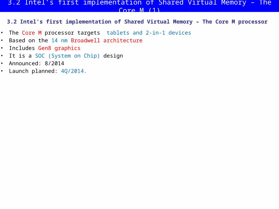
3.2 Intel’s first implementation of Shared Virtual Memory – The Core M processor
• The Core M processor targets tablets and 2-in-1 devices• Based on the 14 nm Broadwell architecture• Includes Gen8 graphics• It is a SOC (System on Chip) design• Announced: 8/2014• Launch planned: 4Q/2014.

Key features of the announced models of the Core M line [15]
3.2 Intel’s first implementation of Shared Virtual Memory – The Core M (2)
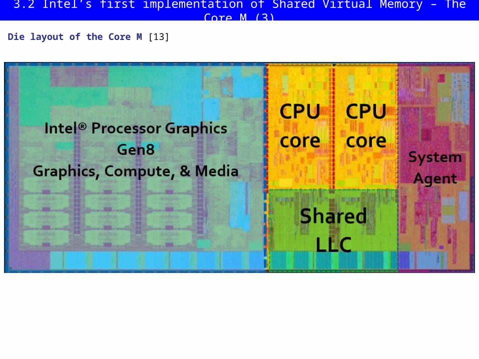
Die layout of the Core M [13]
3.2 Intel’s first implementation of Shared Virtual Memory – The Core M (3)

Block diagram of the Core M [13]
3.2 Intel’s first implementation of Shared Virtual Memory – The Core M (4)

Block diagram of the Gen8 graphics [13]
3.2 Intel’s first implementation of Shared Virtual Memory – The Core M (5)

Each SIMD FPU: 16 x FP32 MADARF: Architectural Register File
Block diagram of an EU [13]
3.2 Intel’s first implementation of Shared Virtual Memory – The Core M (6)

Compute architecture of Core M [13]
3.2 Intel’s first implementation of Shared Virtual Memory – The Core M (7)

4. NVIDIA’s planned introduction of Unified Memory

4. NVIDIA’s planned introduction of Unified Memory (1)
4. NVIDIA’s planned introduction of Unified Memory
NVIDIA planned to introduce Unified Memory in their subsequent Maxwell GPU design, (designated yet as Unified Virtual Memory in the Figure), as seen next.

NVIDIA’s GPU roadmap from 11/2013 [17]
Nevertheless, NVIDIA modified their GPU roadmap in 3/2014 and delayed the introduction of Unified Virtual Memory as shown in the next Figure.
4. NVIDIA’s planned introduction of Unified Memory (2)

Notes
• In their GPU roadmap NVIDIA substituted Volta by Pascal.• Unified Virtual Memory (UVM) support became delayed, instead of Maxwell first Pascal will support this feature. • Beyond UVM Pascal will provide stacked memory (planned already for Volta) and NVlink.
NVIDIA’s updated GPU roadmap from 3/2014 (showing Pascal instead of Volta) [23]
SGEMM: SinGle precision, General Matrix Multiply
4. NVIDIA’s planned introduction of Unified Memory (3)

Main features of NVIDIA’s recent discrete GPU cards [24]
4. NVIDIA’s planned introduction of Unified Memory (4)

NVIDIA’s Tegra roadmap (Based on [18])
4. NVIDIA’s planned introduction of Unified Memory (5)

Planned enhancements for increasing the memory bandwidth for Unified Memory
a) Stacked memoryb) NVlink
4. NVIDIA’s planned introduction of Unified Memory (6)

• HMC is a stacked memory.
• It consists of
• a vertical stack of DRAM dies that are connected using TSV (Through-Silicon-Via) interconnects and
• a high speed logic layer that handles all DRAM control within the HMC, as indicated in the Figure below.
Figure: Main parts of a HMC memory [28]
TSV interconnects
a) Stacked Memory (Hybrid Memory Cube, 3D Memory) at a glance [28]
4. NVIDIA’s planned introduction of Unified Memory (7)

Key features of stacked memories [25]
4. NVIDIA’s planned introduction of Unified Memory (7a)

Speed benefit of stacked memory [25]
4. NVIDIA’s planned introduction of Unified Memory (8)
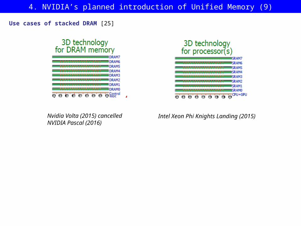
Use cases of stacked DRAM [25]
Nvidia Volta (2015) cancelledNVIDIA Pascal (2016)
Intel Xeon Phi Knights Landing (2015)
4. NVIDIA’s planned introduction of Unified Memory (9)
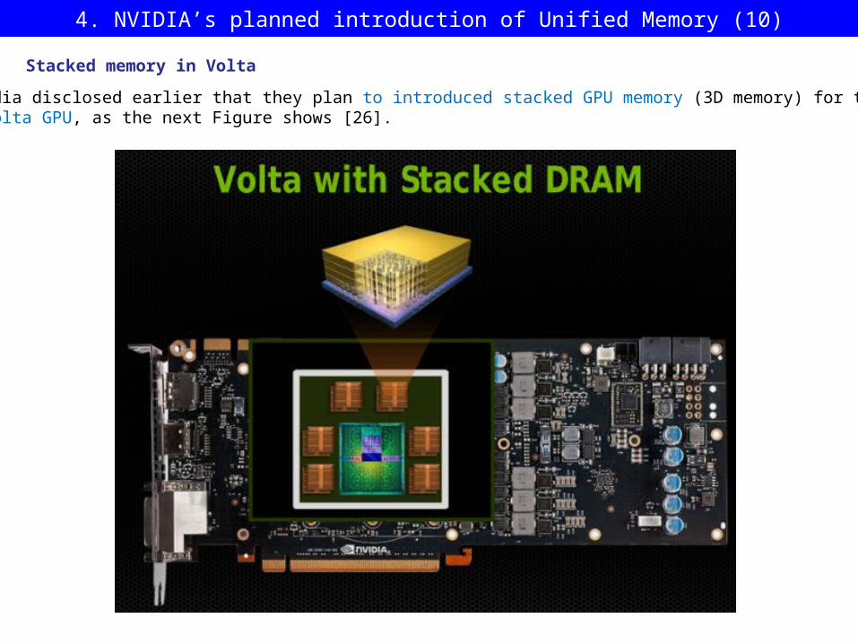
Stacked memory in Volta
Nvidia disclosed earlier that they plan to introduced stacked GPU memory (3D memory) for their Volta GPU, as the next Figure shows [26].
4. NVIDIA’s planned introduction of Unified Memory (10)
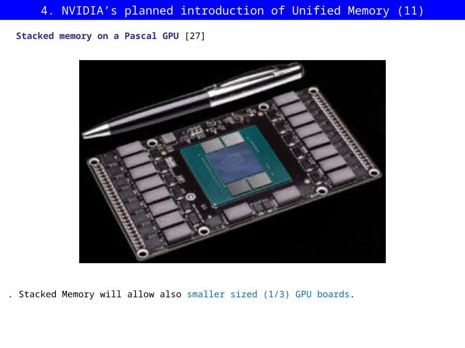
. Stacked Memory will allow also smaller sized (1/3) GPU boards.
Stacked memory on a Pascal GPU [27]
4. NVIDIA’s planned introduction of Unified Memory (11)

b) NVlink [27]
• Announced in 3/2014 by NVIDIA and IBM.
• It is a high speed interconnect with differential lanes and embedded clock.
• The basic building block for NVLink is an 8-lane, differential, bidirectional link providing a bandwidth of 80 to 200 MB/s compared to ~8 GB/s allowed by an 8-lane PCIe 3.0 link.
• NVIDIA intends to introduce NVlink first in their Pascal GPU that is scheduled for 2016.
Figure: Use of Nvlink for connecting GPUs to a CPU [27]
4. NVIDIA’s planned introduction of Unified Memory (12)

5. References

[1]: Wikipedia, Heterogeneous System Architecture, http://en.wikipedia.org/wiki/Heterogeneous_System_Architecture
5. References (1)
[3]: Chu H., AMD heterogeneous Uniform Memory Access, April 30 2013, http://events.csdn.net/AMD/GPUSat%20-%20hUMA_june-public.pdf
[4]: Heterogeneous System Architecture and the HSA Foundation, June 2012, http://www.slideshare.net/hsafoundation/hsa-overview
[5]: AMD’s 2014 A-Series APU, Welcome to the revolution, Jan. 2014, http://new.sliven.net/res/news/129364/Kaveri%20Press%20Deck-v1.01.pdf
[2]: Schroeder T.C., Peer-to-Peer & Unified Virtual Addressing, 2011, http://on-demand.gputechconf.com/gtc-express/2011/presentations/cuda_webinars_ GPUDirect_uva.pdf
[6]: What is Heterogeneous System Architecture (HSA)?, 2014, http://developer.amd.com/resources/heterogeneous-computing/what-is-heterogeneous- system-architecture-hsa/
[7]: Pollice M., Analysis: AMD Kaveri APU and Steamroller Core Architectural Enhancements Unveiled, BSN, March 6 2013, http://www.brightsideofnews.com/news/2013/3/6/analysis- amd-kaveri-apu-and-steamroller-core-architectural-enhancements-unveiled.aspx
[8]: Macri J., Kaveri Design and Architectural Overview, AMD Tech Day, Jan. 2014, http://www.pcmhz.com/media/2014/01-ianuarie/14/amd/AMD-Tech-Day-Kaveri.pdf

[9]: Gasior G., AMD's heterogeneous queuing aims to make CPU, GPU more equal partners, Tech Report, October 22 2013, http://techreport.com/news/25545/amd-heterogeneous- queuing-aims-to- make-cpu-gpu-more-equal-partners
5. References (2)
[11]: Goto H., APU evolution and future memory architecture of AMD Kaveri, PC Watch, Jan. 29 2014, http://translate.google.hu/translate?hl=hu&sl=ja&tl=en&u=http%3A%2F% 2Fpc.watch.impress.co.jp%2Fdocs%2Fcolumn%2Fkaigai%2F20140129_632794.html
[12]: Kerby B., Whitney, Intel's 810 Chipset - Part I, Tom’s Hardware, April 30 1999, http://www.tomshardware.com/reviews/whitney,105-4.html
[13]: Junkins S., The Compute Architecture of Intel Processor Graphics Gen8, IDF 2014, https://software.intel.com/sites/default/files/managed/71/a2/Compute%20Architecture% 20of%20Intel%20Processor%20Graphics%20Gen8.pdf
[10]: Goto H., AMD CPU Transition, 2011, http://pc.watch.impress.co.jp/video/pcw/docs/473/823/p7.pdf
[14]: Smith R., Khronos @ SIGGRAPH 2013: OpenGL 4.4, OpenCL 2.0, & OpenCL 1.2 SPIR Announced, AnandTech, July 22 2013, http://www.anandtech.com/show/7161/khronos- siggraph-2013-opengl-44-opencl-20-opencl-12-spir-announced/3
[15]: Woligroski D., Intel's Broadwell Core M Processor: New Details, SKUs and Specifics, Tom’s Hardware, Sept. 5 2014, http://www.tomshardware.com/news/intel-broadwell-core-m,27596.html
[16]: Harris M., Unified Memory in CUDA 6, NVIDIA Developer Zone, Nov. 18 2013, http://devblogs.nvidia.com/parallelforall/unified-memory-in-cuda-6/

[17]: Smith R., NVIDIA Announces CUDA 6: Unified Memory for CUDA, AnandTech, Nov. 14 2013, http://www.anandtech.com/show/7515/nvidia-announces-cuda-6- unified-memory-for-cuda
5. References (3)
[19]: Rao A., Compute with Tegra K1, GPU Technology Conference, 2014, http://on-demand.gputechconf.com/gtc/2014/presentations/S4906-mobile-compute- tegra-K1.pdf
[20]: Toksvig M., NVIDIA Tegra, http://www.hotchips.org/wp-content/uploads/hc_archives/hc20/2_Mon/HC20.25.331.pdf
[21]: Klug B., Shimpi A.L., NVIDIA Tegra K1 Preview & Architecture Analysis, AnandTech, Jan. 6 2014, http://www.anandtech.com/show/7622/nvidia-tegra-k1/3
[18]: Burke S., Analysis of NVidia's Unified Virtual Memory Roadmap Disappearance & an ARM Future, Gamers Nexus, April 3 2014, http://www.gamersnexus.net/guides/1383-nvidia- unified-virtual-memory-roadmap-tegra-future
[22]: Chester B., Xiaomi Announces the MiPad: The First Tegra K1 Device, AnandTech, May 15 2014, http://www.anandtech.com/show/8022/xiaomi-announces-the-mipad- the-first-tegra-k1-device
[23]: Smith R., NVIDIA Updates GPU Roadmap; Unveils Pascal Architecture For 2016, AnandTech, March 26 2014, http://www.anandtech.com/show/7900/nvidia-updates-gpu-roadmap- unveils-pascal-architecture-for-2016

[24]: Hruska J., Nvidia Maxwell GTX 980 and GTX 970 reviewed: Crushing all challengers, Extreme Tech, Sept. 19 2014, http://www.extremetech.com/computing/190463-nvidia- maxwell-gtx-980-and-gtx-970-review
5. References (4)
[26]: Demerjian C., Nvidia_Volta_mockup, SemiAccurate, May 19 2013, http://semiaccurate.com/2013/05/20/nvidias-volta-gpu-raises-serious-red-flags-for- the-company/nvidia_volta_mockup/
[27]: Foley D., NVLink, Pascal and Stacked Memory: Feeding the Appetite for Big Data, NVIDIA Developer Zone, March 25 2014, http://devblogs.nvidia.com/parallelforall/ nvlink-pascal-stacked-memory-feeding-appetite-big-data/
[25]: Ujaldón M., Many-core GPUs: Achievements and perspectives, 2013, http://icpp2013.ens-lyon.fr/GPUs-ICPP.pdf
[28] - A Revolution in Memory, Micron Technology Inc., http://www.micron.com/products/hybrid-memory-cube/all-about-hmc