sinec l2 - dp spm2 siemens profibus multiplexer · 2016-10-28 · in the event of an error, all...
TRANSCRIPT

SINEC L2 - DP
SPM2 Siemens PROFIBUS Multiplexer
User Description Date Nov 27th, 96
Order No. 6ES7 195-0BB00-8BA0


SINEC L2-DP
(Siemens PROFIBUS Multiplexeraccording to DIN E 19245 Part 3)
Version: V1.3
Date: Nov 27th, 1996
SPM2
User Description

SchnittStellenCenter SPM2
Page 2 Release V1.3 User Description
11/96 Copyright (C) Siemens AG 1997. All rights reserved.
Liability ExclusionWe have tested the contents of this document regarding agreement with thehardware and software described. Nevertheless, deviatations can’t beexcluded, and we are not guaranteeing complete agreement. The data in thisdocument is checked periodically, however. Necessary corrections will becontained in subsequent versions. We gratefully accept suggestions forimprovement.
CopyrightCopyright Siemens AG 1995. All rights reserved.Unless permission has been expressly granted, passing on this document orcopying it, or using and sharing its content, is not allowed. Offenders will beheld liable. All rights reserved, in the event a patent is granted or a utilitymodel or design is registered.
Subject to technical changes.

SPM2 SchnittStellenCenter
User Description Release V1.3 Page 3
Copyright (C) Siemens AG 1997. All rights reserved. 11/96
Table of Contents
1 INTRODUCTION 5
2 OVERVIEW OF FUNCTIONS 6
3 PIN DESCRIPTION 7
3.1 XTAL1 Clock Input 12
3.2 FQ48 12
3.3 RWCONS 12
3.4 KONS 13
3.5 PARASER 13
3.6 TS0...6 143.6.1 INTERDI, -CS, -CLK, -DOD 143.6.2 ACA (AddressChangeAllowed) 143.6.3 XSREE 14
3.7 DIAERROR 15
3.8 NORMOPER 15
3.9 XTRI, XTEMO 15
4 FUNCTION DESCRIPTION OF THE INDIVIDUAL BLOCKS 16
4.1 Watchdog timer 16
4.2 Automatic baud rate detection 16
4.3 EEPROM interface (serial) 174.3.1 EEPROM parameters 174.3.2 EEPROM interface 184.3.3 EEPROM control 19
4.4 Shift register interface 204.4.1 Shift register parameters 204.4.2 Shift register interface 214.4.3 Control of the external shift register 21
4.5 I/O interface 224.5.1 Structure of the diagnostic ports 25
4.6 L2 interface 26
5 TELEGRAM STRUCTURE 28
5.1 Parameter telegram (SET_PARAM) 28

SchnittStellenCenter SPM2
Page 4 Release V1.3 User Description
11/96 Copyright (C) Siemens AG 1997. All rights reserved.
5.2 Configuration telegram (GET_CONFIG) 30
5.3 Diagnostic telegram (SLAVE_DIAG) 31
5.4 Optional services 32
5.5 Other services 32
6 TECHNICAL DATA 33
7 TIMINGS 36
7.1 EEPROM 36
7.2 Shift register 38
7.3 RESET 38
7.4 Consistency signal RWCONS 39
8 ADDRESS DIRECTORY 40
9 CIRCUIT EXAMPLES 41
9.1 Shift register 41
9.2 Wiring example - EEPROM , ext. oscillator , error indicator and RESET 42
9.3 Wiring example - PROFIBUS interface 43
10 BUS CONNECTION 44

SPM2 SchnittStellenCenter
User Description Release V1.3 Page 5
Copyright (C) Siemens AG 1997. All rights reserved. 11/96
1 Introduction
Siemens offers its users some ASICs which support resp. fully handle data communication between theindividual automation stations for simple and fast digital data exchange between programmable logiccontrollers (in accordance with PROFIBUS DIN 19245 Part 1 ). The SPC ( Siemens Profibus Controller ) isbased directly on Layer 1 of the OSI Model and requires an additional microprocessor for implementation ofLayers 2 and 7. This permits all protocol types to be covered at the user end.
The SPC supports active and passive users on the bus system and filters off all external telegrams anderrored wanted telegrams.
However, there are also simple devices, such as switches and thermocouples, in the field of automationwhich do not require a microprocessor for detection of their states.
Two further ASICs with the designation SPM2 (Siemens Profibus Multiplexer, Version 2) and LSPM2 (LeanSiemens Profibus Multiplexer) are available for low-cost adaptation of these devices. The SPM2 operatesas a Slave in the bus system. A Master addresses both via Layer 2 of the 7-Layer Model. After they havereceived an error-free telegram, it automatically generates the requested response telegrams (inaccordance with DIN E 19245, Part 3).
The LSPM2 has the same functions as the SPM2, but with a reduced number of I/O and diagnostic ports.

SchnittStellenCenter SPM2
Page 6 Release V1.3 User Description
11/96 Copyright (C) Siemens AG 1997. All rights reserved.
2 Overview of functions
The SPM2 has input/output ports which can be adapted directly to the periphery for data exchange with theperiphery. The function blocks which the SPM2 contains include the following:
The UART converts the parallel data of the I/O ports to a serial data stream for the L2 bus and vice versa.
The BAUD RATE GENERATOR generates baud rates of 9.6 kBd to 12 MBd. The clock for the baud rategenerator must be supplied by an external clock pulse generator.
Two operating modes are possible: -48 MHz clock and baud rates of 9.6 kBd to 12 MBd-24 MHz clock and baud rates of 9.6 kBd to 6 MBd
The IDLE timer generates the bus idle time which is required for synchronising the listening users.
The integrated watchdog timer monitors the users present for addressability. In the event of an error, allports are set to logical „0“ in order to avoid malfunctions.
The I/O interface provides 8 input/output ports and 2 input ports. Depending on the configuration, the portsserve as data inputs/outputs, diagnostic inputs, configuration inputs and for entering the identificationnumber (see Chapter 4.5).
The micro-sequencer (MS) performs the task of handling telegram communication and evaluating theindividual functions, including automatic baud rate detection.
The USER interface state machine generates control signals for the MS and generates the status indicationwhich the Master can request for evaluation.
The Profibus DP-specific parameters (station address and identification number) may be stored on anexternal EEPROM or serial shift register or may be set directly via the corresponding pins on the SPM2.Use of the individual ports is set via 6 pins on the SPM2. An integrated control logic generates the signalsfor controlling the serial EEPROM or external shift register independently, depending on the external wiringused.
SPM2 SchnittStellenCenter
User Description Release V1.3 Page 7
Copyright (C) Siemens AG 1997. All rights reserved. 11/96
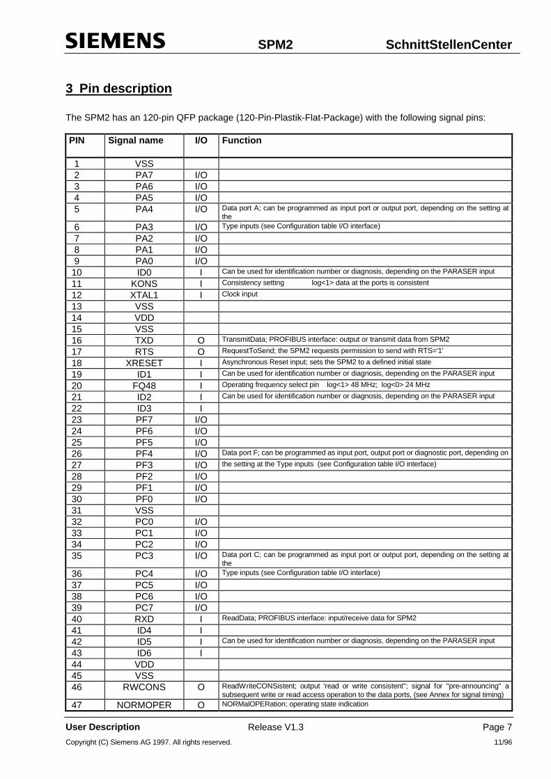
3 Pin description
The SPM2 has an 120-pin QFP package (120-Pin-Plastik-Flat-Package) with the following signal pins:
PIN Signal name I/O Function
1 VSS 2 PA7 I/O 3 PA6 I/O 4 PA5 I/O 5 PA4 I/O Data port A; can be programmed as input port or output port, depending on the setting at
the
6 PA3 I/O Type inputs (see Configuration table I/O interface)
7 PA2 I/O 8 PA1 I/O 9 PA0 I/O 10 ID0 I Can be used for identification number or diagnosis, depending on the PARASER input
11 KONS I Consistency setting log<1> data at the ports is consistent
12 XTAL1 I Clock input
13 VSS 14 VDD 15 VSS 16 TXD O TransmitData; PROFIBUS interface: output or transmit data from SPM2
17 RTS O RequestToSend; the SPM2 requests permission to send with RTS='1'
18 XRESET I Asynchronous Reset input; sets the SPM2 to a defined initial state
19 ID1 I Can be used for identification number or diagnosis, depending on the PARASER input
20 FQ48 I Operating frequency select pin log<1> 48 MHz; log<0> 24 MHz
21 ID2 I Can be used for identification number or diagnosis, depending on the PARASER input
22 ID3 I 23 PF7 I/O 24 PF6 I/O 25 PF5 I/O 26 PF4 I/O Data port F; can be programmed as input port, output port or diagnostic port, depending on
27 PF3 I/O the setting at the Type inputs (see Configuration table I/O interface)
28 PF2 I/O 29 PF1 I/O 30 PF0 I/O 31 VSS 32 PC0 I/O 33 PC1 I/O 34 PC2 I/O 35 PC3 I/O Data port C; can be programmed as input port or output port, depending on the setting at
the
36 PC4 I/O Type inputs (see Configuration table I/O interface)
37 PC5 I/O 38 PC6 I/O 39 PC7 I/O 40 RXD I ReadData; PROFIBUS interface: input/receive data for SPM2
41 ID4 I 42 ID5 I Can be used for identification number or diagnosis, depending on the PARASER input
43 ID6 I 44 VDD 45 VSS 46 RWCONS O ReadWriteCONSistent; output 'read or write consistent''; signal for "pre-announcing" a
subsequent write or read access operation to the data ports, (see Annex for signal timing)
47 NORMOPER O NORMalOPERation; operating state indication

SchnittStellenCenter SPM2
Page 8 Release V1.3 User Description
11/96 Copyright (C) Siemens AG 1997. All rights reserved.
log<1> SPM2 is in DATA_EXCHANGE_Modelog<0> SPM2 is not in DATA_EXCHANGE_Mode

SPM2 SchnittStellenCenter
User Description Release V1.3 Page 9
Copyright (C) Siemens AG 1997. All rights reserved. 11/96
PIN Signal name I/O Function
47 DIAERROR O DIAgnosticERROR; this output is set in the case of external diagnosis
49 ID7 I Can be used for identification number or diagnosis, depending on the PARASER input
50 XCTS I ClearToSend; PROFIBUS interface: the SPM2 is clear to send if the XCTS signal is active(log.<0> active)
51 XTEMO I log<1> must be applied permanently to test pin (Normal mode)
52 XTRI I log<1> must be applied permanently to test pin (Normal mode)
53 PG0 I/O54 PG1 I/O55 PG2 I/O56 PG3 I/O Data port G; can be programmed as input port, output port or diagnostic port, depending on
57 PG4 I/O the setting at the Type inputs (see Configuration table I/O interface)
58 PG5 I/O59 PG6 I/O60 PG7 I/O61 VSS62 PD0 I/O63 PD1 I/O64 PD2 I/O Data port D; can be programmed as input port or output port, depending on the setting at
65 PD3 I/O the Type inputs (see Configuration table I/O interface)
66 PD4 I/O67 PD5 I/O68 PD6 I/O69 PD7 I/O70 PH0 I/O71 PH1 I/O Data port H; can be programmed as input port, output port or diagnostic port, depending on
72 PH2 I/O the setting at the Type inputs (see Configuration table I/O interface)
73 PH3 I/O74 VDD75 VSS76 PH4 I/O77 PH5 I/O78 PH6 I/O79 PH7 I/O80 PI7 I/O81 PI6 I/O82 PI5 I/O83 PI4 I/O Port I, can be configured as diagnostic input or parameter input
84 PI3 I/O (see Configuration table I/O interface)
85 PI2 I/O86 PI1 I/O87 PI0 I/O88 TYP0 I Type setting; the ports of the SPM2 are programmed "approximately" with these pins;
89 TYP1 I (see Configuration table I/O interface)
90 TYP2 I91 VSS92 PB7 I/O93 PB6 I/O94 PB5 I/O95 PB4 I/O Data port B; can be programmed as input port or output port, depending on the setting at
96 PB3 I/O the Type inputs (see Configuration table I/O interface)
97 PB2 I/O98 PB1 I/O99 PB0 I/O

SchnittStellenCenter SPM2
Page 10 Release V1.3 User Description
11/96 Copyright (C) Siemens AG 1997. All rights reserved.
100 PARASER Defines whether a serial memory (EEPROM or shift register) is connected or whether the TSaddress and identification number are applied parallel to the SPM2.log.<1> external serial memory is connected

SPM2 SchnittStellenCenter
User Description Release V1.3 Page 11
Copyright (C) Siemens AG 1997. All rights reserved. 11/96
PIN Signal name I/O Function
101 ID8 I102 ID9 I Can be used for identification number or diagnosis, depending on the PARASER input
103 ID10 I104 VDD105 VSS106 PE7 I/O107 PE6 I/O108 PE5 I/O Data port E; can be programmed as input port, output port, diagnostic port or parameter port,
109 PE4 I/O depending on the setting at the Type inputs (see Configuration table I/O interface)
110 PE3 I/O111 PE2 I/O112 PE1 I/O113 PE0 I/O114 TS0 I115 TS1 I116 TS2 I/O Depending on configuration, these pins are used for connection of a serial external EEPROM
117 TS3 I/O or shift register or for directly setting the TS address.
118 TS4 I/O (see Pin description, Chapter 3.6)
119 TS5 I120 TS6 I

SchnittStellenCenter SPM2
Page 12 Release V1.3 User Description
11/96 Copyright (C) Siemens AG 1997. All rights reserved.
3.1 XTAL1 Clock Input
The SPM2 is operated with an external clock (e.g. crystal oscillator). The Clock signal is connected to theXTAL1 input (see Chapter Connection examples for a connection example with crystal oscillator).Various baud rates are available depending on the Clock.
24 MHz -- 9,6 kBd to 6 MBd48 MHz -- 9.6 kBd to 12 MBd
3.2 FQ48
This input informs the SPM2 of what operating frequency is applied to pins XTAL1.
log.<0> 24 MHzlog <1> 48 MHz
The input must be wired.
3.3 RWCONS
This output signal serves to pre-announce a consistent write or read access operation on the data ports.
Timing for this is described in Chapter 7.4

SPM2 SchnittStellenCenter
User Description Release V1.3 Page 13
Copyright (C) Siemens AG 1997. All rights reserved. 11/96
3.4 KONS
This input defines whether the data is processed consistently at the ports.
When using consistency the master documentations has to be attended!
log <0> Port data is not consistentlog.<1> Port data is consistent
The input must be connected.
3.5 PARASER
PARASER defines whether a serial parameter memory (EEPROM or shift register) is connected to theSPM2 or whether the station parameters (TS address and PNO identification number) are connectedparallel at the pins of the SPM2.
This input also determines the function of various other pins (see Table I/O interface).
log <0> No serial parameter memory is connectedlog.<1> Serial parameter memory is connected
The input must be connected.

SchnittStellenCenter SPM2
Page 14 Release V1.3 User Description
11/96 Copyright (C) Siemens AG 1997. All rights reserved.
3.6 TS0...6
Pins TS0...6 are used as follows depending on the PARASER pin:
PIN Function with PARASER = 0 Function with PARASER = 1
114 TS0 Bit 0 TS address must be connected115 TS1 Bit 1 TS address INTERDI116 TS2 Bit 2 TS address INTERCS117 TS3 Bit 3 TS address INTERCLK118 TS4 Bit 4 TS address INTERDOD119 TS5 Bit 5 TS address ACA120 TS6 Bit 6 TS address XSREE
3.6.1 INTERDI, -CS, -CLK, -DOD
These pins are used for control of a serial parameter memory (EEPROM or shift register) for storing the TSaddress and PNO identification number.(see Chapters 4.3 and 4.4 for a more detailed description).
3.6.2 ACA (AddressChangeAllowed)
With ACA signal active, it is possible, with a corresponding call telegram, to overwrite the EEPROMcontents even with No_Add_Chg bit set (see Telegram structure, Chapter 5.).
log. <1> active TS address can be overwritten in the EEPROM
If the SPM2 is operated with a shift register (XSREE=0), this input has no function.
A defined level must be applied to the pin.
Attention: After Power on you can always overwrite the adress
3.6.3 XSREE
This input defines whether the SPM2 is operated with an external EEPROM or external shift register.
log. <0> ext. shift registerlog. <1> ext. EEPROM
The input must be wired.

SPM2 SchnittStellenCenter
User Description Release V1.3 Page 15
Copyright (C) Siemens AG 1997. All rights reserved. 11/96
3.7 DIAERROR
This output serves to signal a diagnostic error and can be used to activate an LED. The output driver poweris 4 mA.
log.<0> no diagnostic errorlog.<1> diagnostic error, i.e. a log.<0> is applied to one of the diagnostic ports
Note: See Chapter 4.5 for further information on diagnosis.
3.8 NORMOPER
This output indicates the operating state of the SPM2 on the Profibus L2 and can be used to activate anLED. The output driver power is 4 mA.
log.<0> SPM2 is not in DATA_EXCHANGE_Modelog.<1> SPM2 is in DATA_EXCHANGE_Mode
3.9 XTRI, XTEMO
Note: VDD must be applied to the XTRI and XTEMO pins.
SchnittStellenCenter SPM2
Page 16 Release V1.3 User Description
11/96 Copyright (C) Siemens AG 1997. All rights reserved.
4 Function description of the individual blocks
4.1 Watchdog timer
If malfunctions or disturbances occur on the bus line, it may be the case that the SPM2 does not receive atelegram and, thus, the module’s ports can no longer be operated. A WD is integrated in order to detect thissituation. The WD timer is used initially for automatic baud rate detection after Reset. When the correctbaud rate has been detected, the MS switches the WD timer automatically to normal mode (Watchdogmode).
If a timeout of the timer occurs, i.e. no valid telegram detected, all outputs are reset ("0") and the systembranches automatically to the automatic baud rate detection function.
The timeout time can be programmed in the COM-ET200. It is possible to select a value between 2 ms and650 s, regardless of the set baud rate, thus permitting adaptation to the relevant system conditions.
The watchdog timeout times which can be set are calculated as follows:
T(WD) = factor * WD_1 * WD_2 Time factors 1 ms or 10 ms can be set via the parameterassignment telegram in the User_Prm_Data (see Telegramstructure, Chapter 5.).
Setting WD_1=WD_2=1 is not permitted. In addition, neither WD_1 nor WD_2 may be 0!
4.2 Automatic baud rate detection
The SPM2 is capable of automatically detecting the baud rate. The MS defaults automatically to automaticbaud rate detection after each Reset and after timeout of the WD timer. The timeout time is set permanentlyto 16384 Tbits for this purpose. No ports are manipulated during detection.
The MS always starts detection of the set baud rate with the highest baud rate. If no SD1, SD2 or SD3telegram has been received completely and error-free during the timeout time, detection is continued withthe next lower baud rate. This telegram may be destined for any user.
After the correct baud rate has been detected, the SPM2 waits one minute for a parameter assignmenttelegram destined for its address (DA=TS). If a Set_Prm_telegram is received during this time, the SPM2changes to Normal mode. Otherwise it resumes the baud rate detection function.
If the SPM2 detects an SD4 telegram dur ing baud rate search, this means that the baud rate has notyet been detected. However, the MS does not change to the next lower baud rate but continuesdetection with the currently set baud rate. The SD4 telegrams are filtered in Normal mode.

SPM2 SchnittStellenCenter
User Description Release V1.3 Page 17
Copyright (C) Siemens AG 1997. All rights reserved. 11/96
4.3 EEPROM interface (serial)
If an EEPROM is used (pin XSREE=1), the station add ress and the ID number are stored in theEEPROM. The station add ress can be transferred to the EEPROM via the ET 200 hand-held operatorcontrol unit.
4.3.1 EEPROM parameters
The SPM2 integrates a controller for a serial ext. EEPROM. Only one 16-bit word is ever stored as theparameter (EEPROM address 0H) or only two 16-bit words are ever read as the parameter (address00H,01H).
Assignment EEPROM word 015 14 13 12 11 10 9 8 7 6 5 4 3 2 1 0
No_Ad TS address0 0 0 0 0 0 0 0 d_Chg X X X X X X X
Assignment EEPROM word 115 14 13 12 11 10 9 8 7 6 5 4 3 2 1 0
ID numberX X X X X X X X X X X X X X X X
The ID number must be written to the EEPROM before connecting to the SPM2 since only the TS addresscan be changed during write access via the SPM2. Both data words are accessed only during readoperations, i.e. an EEPROM programmed with the ID number must be used for production of a unit.
ID number:The ID number serves as a unique identification of a DP Slave device type on the bus. An ID number isrequired for all DP Slave devices when reading diagnostic data, when writing parameter assignment dataand when changing the station address via the bus. The ID number makes it possible for the DP Masters toidentify the DP Slaves with minimal protocol effort.
An individual ID number is issued by the PNO (PROFIBUS User Organisation) for each device type. This IDnumber is not a serial number. Once a manufacturer has received an ID number for a device type from thePNO, he may use this number for each device of this type produced without having to ask for an ID numberagain each time from the PNO.
A separate ID number does not need to be applied for each revision level of devices which are basicallyidentical but which differ as regards the number of inputs and outputs. The precondition is that the productcan be described as a modular device in the GSD (device master file).
During the boot phase or after a RESET, the SPM2 accepts the parameters (word 0, word 1) serially froman EEPROM and loads them into its internal parameter register.
The following values are permitted: TS address: 1.... 126DID number: all 16-bit values (as assigned by the PNO)
If the SPM2 detects an illegal address (0 or 127D) when reading in, the MS automatically writes the defaultvalue TS=126D and No_Add_Chg=0 to the EEPROM. This permits parameter assignment of the stationaddress with the corresponding tool (COM ET200).

SchnittStellenCenter SPM2
Page 18 Release V1.3 User Description
11/96 Copyright (C) Siemens AG 1997. All rights reserved.
4.3.2 EEPROM interface
The EEPROM control logic contained in the SPM2 supports only serial modules with 5V supply, 16-bitorganisation and integrated control logic. The control signals for EEPROMs with designation 93C46/47 orcompatible EEPROMs (e.g. type OKI Datacode 16811 or higher) are generated. An ERASE/WRITEENABLE cycle precedes each write cycle since the module is generally in DISABLE state after a powerfailure or power fade (i.e. it cannot be erased or written).
The SPM2 internally triggers a write/read cycle with two flags (RD-EEPROM and WR-EEPROM),whereupon the EEPROM controller generates the corresponding control sequences for the output pins.When the cycle is completed, the controller acknowledges this by resetting the flags.
Signal name I/O Function Status afterRESET XSREE=„1“
INTERCS O Chip-select for EEPROM log. <0>INTERCLK O Clock signal for EEPROM log. <0>INTERDI I DATA IN (Read EEPROM) (ST), READY
after programming-
INTERDOD O Data Out (Write EEPROM) log. <0> ST = Schmitt-Trigger
After the micro-sequencer (MS) has issued a read request to the controller, the read data is stored in a shiftregister and acknowledged by resetting the RD flag.
When writing the memory, the MS loads the data of the station address directly into the shift register of theEEPROM controller, provided the telegram has been received error-free by the SPM2. During the writeoperation, the MS continues normal program processing. As soon as the memory chip has accepted thedata, the controller acknowledges this by resetting the WD flag. If the SPM2 receives a request to write theEEPROM, it acknowledges reception of the call telegram and then branches to the baud rate detectionfunction. The telegram results in a negative acknowledgement „RS“ if no EEPROM is connected.
A RESET during writing leads to undefined data in the EEPROM.After Power on you can always overwrite the adress.

SPM2 SchnittStellenCenter
User Description Release V1.3 Page 19
Copyright (C) Siemens AG 1997. All rights reserved. 11/96
4.3.3 EEPROM control
Since the memory has a serial interface, the data, addresses and also the commands for switching over tothe various operating modes must be transferred to it serially. The specified module awaits a 2-bit Op codeafter a start bit (log. "1") and then a 6-bit address, i.e. 9 bits, in order to switch to the corresponding mode.Data is read or written only after this.
The following Op codes are generated:
Command Start bit/Opcode Address (binary)
READ WORD 110 000000 or. 000001ERASE/WRITE-ENABLE 100 110000
WRITE WORD 101 000000
An erase cycle is not required since the memory overwrites the corresponding word when writing.
The word with address 000 000Bin is generally addressed in the EEPROM, but an Erase/Write-Enable cycleis executed before each write access operation since the module is generally in Erase/Write-Disable modeafter the power is restored.
The integrated controller of the SPM2 generates a clock (INTERCLK) and a Chip-Select signal (INTERCS)with the corresponding timing and clocks the control bits and data out sequentially when writing or into aninternal shift register when reading.
min. 4µs
INTERCLKClock for EEPROM
internal clock min. 2µs
A read access operation takes 200 µs for one complete read cycle. A write cycle requires 100 µs, in additionto the programming time of approx. 10 ms per word.
Note : See Chapter 8 for a circuit example of connection of an EEPROM.

SchnittStellenCenter SPM2
Page 20 Release V1.3 User Description
11/96 Copyright (C) Siemens AG 1997. All rights reserved.
4.4 Shift register interface
Besides the option of connecting an external EEPROM, the SPM2 can also be wired with an external shiftregister (PARASER=1, XSREE=0). In this case, the integrated shift register controller independentlygenerates control sequences for shift registers with designation 74HC165 or compatible shift registers.
4.4.1 Shift register parameters
The internal shift register of the SPM2 is written serially via bit position 23. The data are shifted to the rightdepending on the number of clock pulses still pending, i.e. the contents of position 23 are stored in bit 22,and the contents of position 22 are stored in bit 21 etc.
The following data sequence must be observed in this case at the serial data input (INTERDI):
first bit 0 (TS address) then bit 1 TS , bit 2 TS, bit 3 ...........bit 0 ID no, bit 1 ID no.,......etc.
TS addressBCD-coded
167
INTERDI
BCD-BINARY convertor(internal)
16 bit ID number TS-Adresse, binary coded
Serial data inputLSPM2
ID number
Shift direction of the internal shift register (LSPM2)
LowHigh
7 6 5 4 3 2 1 0 7 6 5 4 3 2 1 0 7 6 5 4 3 2 1 0
externalshiftregister
74HC165 23 22 21 20 19 18 17 16 15 14 13 12 11 10 9 8 7 6 5 4 3 2 1 0
A total of 24 bits must be stored in the external shift register: 16 bits for the ID number and 8 bits forthe TS address.
The TS address must be set BCD-coded externally (values permitted are 1Dec to 99Dec). If the SPM2detects the illegal value 0Dec or an inadmissible BCD value, the TS address is assigned 126Dec.
The externally set address is converted BCD-BINARY in the SPM2 in order to permit the Slaveaddress (TS) to be compared with the binary-coded destination address (DA) of the call telegram.

SPM2 SchnittStellenCenter
User Description Release V1.3 Page 21
Copyright (C) Siemens AG 1997. All rights reserved. 11/96
4.4.2 Shift register interface
The shift register controller is a block which is independent of the rest of the module and which is triggeredonly by the micro-sequencer (MS). The MS triggers a read cycle with a ReadShift flag, whereupon the shiftregister controller generates the corresponding control sequences for the interface pins. When the readcycle is complete, the controller acknowledges this by resetting the ReadShift flag.
If an external shift register is connected, the sequencer issues a read request to the contr oller aftera RESET in order to accept the data in its parameter register.
Signal name I/O Function Status afterRESET XSREE=„0“
INTERCS O Clock Enable für Schieberegister log. <1>INTERCLK O Taktsignal für Schieberegister log. <0>INTERDI I DATA IN (Read Schieberegister), (ST) -
INTERDOD O Übernahmesignal für Daten insext. Schiebereg. (parallel load)
log. <1>
ST=Schmitt trigger
4.4.3 Control of the external shift register
The sequential control generates a clock (INTERCLK), a Clock Enable signal (INTERCS) and an Acceptsignal (INTERDOD) with the required timing and clocks the data sequentially into an SPM2-internal shiftregister when reading.
When reading, the data is first loaded in parallel into the external shift register with the INTERDOD signal.From there, the data is clocked serially into the SPM2-internal shift register (see Chapter Timing for timing).
min. 4µs
INTERCLKClock for shift register
internal clock min. 2µs
The shift register controller operates with the same clock frequency as the EEPROM controller, i.e. 250 kHz.A read access operation takes 96 µs.
Note: See Chapter 8 for a circuit example.

SchnittStellenCenter SPM2
Page 22 Release V1.3 User Description
11/96 Copyright (C) Siemens AG 1997. All rights reserved.
4.5 I/O interface
The following ports are available to the user for detection and output of the various signals of a processsequence on site:
Note: A distinction must be made between the designation data port and SPM2 port.
− four 8-bit input/output ports ( A, B, C, Df)− three 8-bit data ports (F, G, H), either input/output or diagnostic− one 8-bit input/output port (E) or diagnostic port (I) -- depending on whether extended diagnosis is
set− two 8-bit general diagnostic ports (J, K) -- only if a serial parameter memory is used.
The 8 programmable data ports have SYNC and FREEZE capability, i.e. none update of the inputs(including diagnostic inputs) are forwarded to the Master until a FREEZE command is received and theoutputs are not updated by the Master until after a SYNC command (see Chapter Telegram structure) ifSYNC and FREEZE mode is active.
The „approximate“ configuration of the SPM2 ports depends on the setting at the Type pins 0...2 and thePARASER input. It defines how the SPM2 ports are used (data ports and/or parameter inputs). In addition,these pins are used to set „Extended diagnosis“ mode. The table below shows the coding of the individualconfigurations.
Attention: Please confirm that the Typ Pins are always set if Power off.
none serial parameter memory (PARASER=0)none extended diagnostic
Type pins 2..0 (0xx Bin or x0x Bin )extended diagnostic
Type pins 2..0 (11x Bin )SPM2 port Pins: using data port SPM2 port Pins: using data portPort A-D ←→ 0...7 I/O data Port A-D Port A-D ←→ 0...7 I/O data Port A-D
Port E ←→ 0...7 I/O data Port E Port E → 0 IDENT 11→ 1 IDENT 12
Port F-H ←→ 0...7 I/O data Port F-H → 2 IDENT 13→ 3 IDENT 14
Port I → 0 IDENT 11 → 4 TYPE 3→ 1 IDENT 12 → 5 TYPE 4→ 2 IDENT 13 → 6 TYPE 5→ 3 IDENT 14 → 7 IDENT 15→ 4 TYPE 3→ 5 TYPE 4 Port F-H → 0...7 Diagnosis Port F-H→ 6 TYPE 5→ 7 IDENT 15 Port I → 0...7 Diagnosis Port I
Port ID → 0...10 IDENT 0...10 Port ID → 0...10 IDENT 0...10

SPM2 SchnittStellenCenter
User Description Release V1.3 Page 23
Copyright (C) Siemens AG 1997. All rights reserved. 11/96
serial parameter memory (PARASER=1)none extended diagnostic
Typ pins 2..0 (0xx Bin or x0x Bin )extended diagnosticTyp pins 2..0 (11x Bin )
SPM2 port Pins using data port SPM2 port Pins using data portPort A-D ←→ 0...7 I/O data Port A-D Port A-D ←→ 0...7 I/O data Port A-D
Port E ←→ 0...7 I/O Data Port E Port E → 0 Group dia. Port K(0)→ 1 Group dia. Port K(1)
Port F-H ←→ 0...7 I/O Data Port F-H → 2 Group dia. Port K(2)→ 3 Group dia. Port K(3)
Port I → 0 Group dia. Port K(0) → 4 TYPE 3→ 1 Group dia. Port K(1) → 5 TYPE 4→ 2 Group dia. Port K(2) → 6 TYPE 5→ 3 Group dia. Port K(3) → 7 Group dia. Port K(7)→ 4 TYPE 3→ 5 TYPE 4 Port F-H → 0...7 Diagnose Port F-H→ 6 TYPE 5→ 7 Group dia. Port K(7) Port I → 0...7 Diagnose Port I
Port ID → 0...7 Group dia. Port J(0:7) Port ID → 0...7 Group dia. Port J(0:7)
Port ID → 8...10 Group dia. Port K(4:6) Port ID → 8...10 Group dia. Port K(4:6)
The „precise" configuration is set via the Type pins 3..5 dependence on Type pins 0..2. Data ports which arenot used (identified by a dash in the table) are programmed as Output by default and may not be connectedon the PC board. The advantage by comparison with programming as Input is that no pull-up resistors orpads with internal pull-up resistors are required (see Chapter Technical data for characteristic data of theinput/output ports).

SchnittStellenCenter SPM2
Page 24 Release V1.3 User Description
11/96 Copyright (C) Siemens AG 1997. All rights reserved.
I = Input O=Output D=Diagnosis -=not used
none extended diagnostic Data portsNr. TYP 2...0 Port I 6...4 A B C D E F G H 0 000 000 I I I I I I I I 1 000 001 I I I I I I I - 2 000 010 I I I I I I - - 3 000 011 I I I I I - - - 4 000 100 I I I I - - - - 5 000 101 I I I - - - - - 6 000 110 I I - - - - - - 7 000 111 I - - - - - - - 8 001 000 O I I I I I I I 9 001 001 O I I I I I I - 10 001 010 O I I I I I - - 11 001 011 O I I I I - - - 12 001 100 O I I I - - - - 13 001 101 O I I - - - - - 14 001 110 O I - - - - - - 15 001 111 O - - - - - - - 16 010 000 O O I I I I I I 17 010 001 O O I I I I I - 18 010 010 O O I I I I - - 19 010 011 O O I I I - - - 20 010 100 O O I I - - - - 21 010 101 O O I - - - - - 22 010 110 O O - - - - - - 23 010 111 O O O O O O O O 24 011 000 O O O I I I I I 25 011 001 O O O I I I I - 26 011 010 O O O I I I - - 27 011 011 O O O I I - - - 28 011 100 O O O I - - - - 29 011 101 O O O - - - - - 30 011 110 - - - - - - - - 31 011 111 - - - - - - - - 32 100 000 O O O O I I I I 33 100 001 O O O O I I I - 34 100 010 O O O O I I - - 35 100 011 O O O O I - - - 36 100 100 O O O O - - - - 37 100 101 O O O O O O I I 38 100 110 - - - - - - - - 39 100 111 - - - - - - - - 40 101 000 O O O O O I I I 41 101 001 O O O O O I I - 42 101 010 O O O O O I - - 43 101 011 O O O O O - - - 44 101 100 O O O O O O O I 45 101 101 O O O O O O I - 46 101 110 O O O O O O O - 47 101 111 O O O O O O - -
extended diagnostic Data portsNr. TYP 2...0 Port E 6...4 A B C D F G H I 48 110 000 I - - - Diag. - - - 49 110 001 I I - - Diag. Diag. - - 50 110 010 I I I - Diag. Diag. Diag. - 51 110 011 I I I I Diag. Diag. Diag. Diag. 52 110 100 O - - - Diag. - - - 53 110 101 O O - - Diag. Diag. - - 54 110 110 O O O - Diag. Diag. Diag. - 55 110 111 O O O O Diag. Diag. Diag. Diag. 56 111 000 O I - - Diag. Diag. - - 57 111 001 O O I - Diag. Diag. Diag. - 58 111 010 O O O I Diag. Diag. Diag. Diag. 59 111 011 O I I - Diag. Diag. Diag. - 60 111 100 O O I I Diag. Diag. Diag. Diag. 61 111 101 O I I I Diag. Diag. Diag. Diag. 62 111 110 - - - - - - - - 63 111 111 - - - - - - - -

SPM2 SchnittStellenCenter
User Description Release V1.3 Page 25
Copyright (C) Siemens AG 1997. All rights reserved. 11/96
4.5.1 Structure of the diagnostic ports
If „Extended diagnosis“ is set, the user has 4 diagnostic ports (F-I) which can be used for bit-serial diagnosis for thedata ports (A-D) for instance. If a serial parameter memory is connected to the SPM2 (PARASER=1), two furtherdiagnostic ports (J and K) are available for general diagnosis.
The diagnostic ports are always read in conjunction with the data ports. This permits a specific I/O mode tobe assigned to the diagnoses.
If programmed via the Type pins, the SPM2 has max. four channel diagnostic ports (ports F-I) with the aidof which each of the I/O ports can be monitored (ports A-D). If ports F-I are set as diagnostic ports, alog.<0> level at one of the pins always results in a DIA_ERROR which is forwarded internally in the SPM2as log.<1>.
The channel diagnostic ports can also be masked channel-serially (each bit) via mask registers. All masksare inactive after a Reset. An error (log.<0>) at a channel diagnostic port is forwarded only if thecorresponding mask bit is set to zero (see also Chapter 5 Telegram structure SET_PARAM).
IMPORTANT: If a TYPE configuration without diagnosis is set, the mask bytes of the corres pondingports must be programmed to 00 HEX!
The general diagnostic ports (J and K) are always available as user-specific diagnostic ports with 8 bits if aserial parameter memory (PARASER=1) is used. The general diagnostic ports are non-maskable. Twooperating modes which can be set by the user via the parameter flag ENA_SAMMEL_DIA are possible forport J (see Telegram structure, Chapter 5).
Flag=log.<0> log<0> at a pin of port J results in a DIA_ERROR (DIAERROR output is set to log.<1>)
Flag=log.<1> Errors at pins J(0) to J(7) set the DIA_ERROR only if a channel diagnostic error is alsoapplied to port F, G, H or I.
An error at port K always leads to a DIA_ERROR. (regardless of the channel diagnostic ports F-I).
However, the user can also use all diagnostic ports for user-specific diagnosis. A log. <0> at a diagnosticinput corresponds to a diagnostic error and sets the output pin DIA-ERROR on the SPM2 to log. <1>.Output DIA-ERROR remains set until an error level is no longer applied to the diagnostic ports. The pin canbe used to drive an LED. The driver power of the output is 4 mA.
In order to prevent unwired inputs of external diagnostic hardware leading permanently to a DIA_ERROR,the SPM2 has an internal logic. This logic compares the current diagnostic data with the data last read inand generates an error only if a diagnostic change has occurred, i.e. each change is sent to the Master onlyonce.
+5V must be applied via pull-up resistors to all unused inputs of the group diagnostic port and theprogrammed channel diagnostic port.

SchnittStellenCenter SPM2
Page 26 Release V1.3 User Description
11/96 Copyright (C) Siemens AG 1997. All rights reserved.
4.6 L2 interface
Transmission is performed in operating mode RS485 (RS485 physical).The SPM2 has the following pins for this:
Signal name I/O Type Function
RTS O CMOS Request to SendTXD O CMOS Transmit dataRXD I CMOS Receive data
XCTS O CMOS Clear to Send
Before sending, the SPM2 sets the RTS signal to "1" and then loads the transmit buffer of the UART withthe 1st character. The UART delays the first telegram character until signal CTS is active. CTS is no longerpolled during telegram transmission. On completion of transmission (buffer empty stop bit is send), the RTSis reset. The XCTS pin must be set to log.<0> during operation.
Switching times:
No. Symbol Parameter min. Unit
1 TsRTS (TXD) RTS ↑ to TXD (Setup-Time) 2 TBit*2 ThRTS (TXD) RTS ↓ to TXD (Hold-Time) 2 TBit*
*: 1 Tbit = 104µs at 9,6kBd, 1 TBit = 83ns at 12MBd
Timing:
RTS
TXD
1 2

SPM2 SchnittStellenCenter
User Description Release V1.3 Page 27
Copyright (C) Siemens AG 1997. All rights reserved. 11/96
The L2 interface is designed as in 9-pin SUB D connector with the following pin assignment:
Pin 1 - not usedPin 2 - not usedPin 3 - B linePin 4 - Request to Send (RTS)Pin 5 - Ground 5V (M5)Pin 6 - 5V potential (P5 floating approx. 100 mA)Pin 7 - not usedPin 8 - A linePin 9 - not used
The line screen must be connected to the housing.
The pin assignment of the free pins can be used optionally in accordance with DIN E 19245, Part 3.
Note: See Chapter 8 for a circuit example.

SchnittStellenCenter SPM2
Page 28 Release V1.3 User Description
11/96 Copyright (C) Siemens AG 1997. All rights reserved.
5 Telegram structure
The SPM2 is a passive Slave user of PROFIBUS-DP. Required response telegrams are generated by theSPM2 independently as soon as it has received a telegram destined for it free of errors from the Master.Telegram communication between Master and Slave has been kept simple and forms only a subset of thepossible PROFIBUS telegrams.
In „normal mode“ the SPM2 processes only error-free SD1, SD2 and SD3 telegrams (StartDelimiterwith value 10 HEX , 68HEX and A2 HEX ) directed to it (correct TS address). Other telegrams are filtered.
Only special features of the telegrams which it is essential to observe when using an SPM2 Slave aredescribed below.
5.1 Parameter telegram (SET_PARAM)
The Master transfers parameter assignment data to the SPM2 with this telegram. 5 bytes USER parameterdata must be transferred to the SPM2 in addition to the 7 parameter bytes.
Byte Bit position Designation7 6 5 4 3 2 1 0
6
7 0 0 0 0EN_
Sammel_Dia
WD_Base 0 0 User_Def_PRM1
8 Mask for Diaport1
9 Mask for Diaport2
10 Mask for Diaport3
11 Mask for Diaport4

SPM2 SchnittStellenCenter
User Description Release V1.3 Page 29
Copyright (C) Siemens AG 1997. All rights reserved. 11/96
Byte 0-6: Parameter assignment data, see DIN E 19425, Part 3
Byte 7: User_Def_PRM1
Bit 0,1: must be set to 0
Bit 2: The WD base bit defines the timebase with which the watchdog is clocked´0´= timebase 10 ms ´1´= timebase 1 msstatus after Reset : 0 (timebase 10ms
Bit 3: This bit activates General diagnosis mode.Status after Reset: 0
EN_Sammel_Dia = 0 A general diagnostic error of port J is always signalledEN_Sammel_Dia = 1 An error at pins J0-J7 is signalled to the Master only if a channel
diagnostic error of port F, G, H or I also occurs.
However, error changes at the channel diagnostic ports and portK are still signalled immediately.
IMPORTANT: If a type configuration without channel diagnosis (port F,G,H or I) isset, EN_Sammel_Dia must be programmed as 0!
Bit 4-7: must be set to 0
Byte 8, 9, 10, 11: Mask bytes for diagnostic ports
Byte 8 contains the mask bits for diagnostic byte 1 (port F)Byte 9 contains the mask bits for diagnostic byte 1 (port G)Byte 10 contains the mask bits for diagnostic byte 1 (port H)Byte 11 contains the mask bits for diagnostic byte 1 (port I)
The mask bits are assigned to the corresponding bit positions of the diagnostic ports. A ´1´ at thecorresponding bit position masks diagnosis, i.e. these bits are masked. All masks are clearedafter Reset.
IMPORTANT: If a type configuration without diagnosis is set, the mask bits must beprogrammed as 00 HEX!
Important: The DP-Master has to send 5 octet USER_PRM_DATA to the SPM2. If the Master onlysends 7 octet whole p arameter-telegram, the SPM2 accepts this telegram, but doesn`t take theparameters Watchdog and Group!

SchnittStellenCenter SPM2
Page 30 Release V1.3 User Description
11/96 Copyright (C) Siemens AG 1997. All rights reserved.
5.2 Configuration telegram (GET_CONFIG)
The Master transfers the configuration data to the SPM2 with this telegram. The SPM2 always expects 2code bytes. The following sequence must be observed.
If consistency is set via the KONS pin, the SPM2 alw ays assumes overall byte consistency whenchecking the configuration.
Byte Bit position Designation7 6 5 4 3 2 1 0
0 0/1 0 0/1 0 0 0/1 0/1 0/1 Code byte_Outputs
1 0/1 0 0 0/1 0 0/1 0/1 0/1 Code byte_Inputs
Byte 0: Code byte_OutputsFollowing values permitted:
Byte 1: Code byte_InputsFollowing values permitted:
without consistency overall consistency00Hex with 0 outputs 00Hex with 0 outputs20Hex with 1 output A0Hex with 1 output21Hex with 2 outputs A1Hex with 2 outputs22Hex with 3 outputs A2Hex with 3 outputs23Hex with 4 outputs A3Hex with 4 outputs24Hex with 5 outputs A4Hex with 5 outputs25Hex with 6 outputs A5Hex with 6 outputs26Hex with 7 outputs A6Hex with 7 outputs27Hex with 8 outputs A7Hex with 8 outputs
without consistency overall consistency00Hex with 0 inputs 00Hex with 0 inputs10Hex with 1 input 90Hex with 1 input11Hex with 2 inputs 91Hex with 2 inputs12Hex with 3 inputs 92Hex with 3 inputs13Hex with 4 inputs 93Hex with 4 inputs14Hex with 5 inputs 94Hex with 5 inputs15Hex with 6 inputs 95Hex with 6 inputs16Hex with 7 inputs 96Hex with 7 inputs17Hex with 8 inputs 97Hex with 8 inputs

SPM2 SchnittStellenCenter
User Description Release V1.3 Page 31
Copyright (C) Siemens AG 1997. All rights reserved. 11/96
5.3 Diagnostic telegram (SLAVE_DIAG)
The SPM2 sends diagnostic data to the Master with this telegram. ´1´ at a bit position signifies that thecorresponding event has occurred.
A further 7 bytes of external diagnostic data, described in the following table, are sent by the SPM2, inaddition to the 6 bytes diagnostic data. Diagnostic data is transferred only after a change of the pendingdata. One exception to this is Freeze mode.
IMPORTANT: If Freeze mode is activated, the diagnostic data is also frozen. An update is thus sent to theMaster not with a change in diagnostic data but only after a further ´Freeze´.
Byte Bit position Designation7 6 5 4 3 2 1 0
5
6 0 0 0 0 0 1 1 1 Diag_Header
7 PJ7 PJ6 PJ5 PJ4 PJ3 PJ2 PJ1 PJ0Port diagnosis(port J)
8 PK7 PK6 PK5 PK4 PK3 PK2 PK1 PK0Port diagnosis(port K)
9 PF7 PF6 PF5 PF4 PF3 PF2 PF1 PF0Port diagnosis(port F)
10 PG7 PG6 PG5 PG4 PG3 PG2 PG1 PG0Port diagnosis(port G)
11 PH7 PH6 PH5 PH4 PH3 PH2 PH1 PH0Port diagnosis(port H)
12 PI7 PI6 PI5 PI4 PI3 PI2 PI1 PI0Port diagnosis(port I)
Byte 6: Diag_HeaderThis byte contains the SPM2-specific number of external diagnostic bytes, i.e. value 07HEX is enteredat this point on the SPM2.
Byte 7, 8: General diagnostic port J, K (only if PARASER=1)
This byte contains the diagnostic data of the signals applied to ports J, K. A diagnostic error at one ofthe pins (log.<0>) is forwarded inverted, i.e. the error is indicated at the corresponding bit positionwith ´1´.
Byte 9, 10, 11, 12: Kanal-Diagnose Port F-I
These bytes contain the diagnostic data of the signals applied to ports F to I. A diagnostic error at oneof the pins (log.<0>) is forwarded inverted, i.e. the error is indicated at the corresponding bit positionwith ´1´. If no extended diagnosis is set via the Type coding, value 00HEX is always entered at thispoint.

SchnittStellenCenter SPM2
Page 32 Release V1.3 User Description
11/96 Copyright (C) Siemens AG 1997. All rights reserved.
5.4 Optional services
The SPM2 basically supports SYNC and FREEZE mode, i.e. if a SYNC or FREEZE is set in theGlobal_Contol_Service, this function is executed.
Note: If FREEZE mode is activated, the diagnostic data are also frozen. A change is not s ignalled tothe Master until a further FREEZE is transmitted.
5.5 Other services
The SPM2 supports services Set_Slave_Adress (if using a serial EEPROMs), Read_Inputs, Read_Outputs,Get_Config.
With the service Read_Inputs only can be got actual values, if after changing inputs a DATA_EXCHANGEtelegram was answered by the SPM2.

SPM2 SchnittStellenCenter
User Description Release V1.3 Page 33
Copyright (C) Siemens AG 1997. All rights reserved. 11/96
6 Technical data
Maximum limit values
Parameter Desig. Min Max Unit
Supply Voltage VDD VSS * - 0.3 7,0 VLeakage Power Pmax 570 mWInput Voltage VI VSS* - 0.3 VDD + 0.3 VInput Current II - 10 + 10 mAStorage Temperature Tstg - 40 + 125 oCJunction Temperature TJ + 125 oC
* VSS = 0V
Important: Long-term operation with these values reduces the module’s service life.
Permitted operating ratings
Parameter Desig. Min Type Max Unit
Supply Voltage VDD 4.75 5.0 5.25 VInput High Voltage VIHC 3.5 - - VInput Low Voltage VILC - - 1.5 VSchmitt trigger:Input High Voltage VIHC 4 - - VInput Low Voltage VILC - - 1.0 VOperating Temperature Top - 40 + 55 oC
DC specification of the I/O driver
Parameter Desig. Condition Min Type Max Unit
Output High Voltage VOH - VDD - 0,8 VOutput Low Voltage VOL - 0,4 VInput Leakage Current ILI - - 10 10 µA
Signal line Driver type Driver strength max. cap. load
PA 7 ....0 to PH 7 ....0 Tristate 4 mA 50 pFTXD Tristate 8 mA 50 pFRTS Tristate 8 mA 50 pF
NORMOPER Tristate 4 mA 50 pFDIAERROR Tristate 4 mA 50 pFINTERCLK Tristate 4 mA 50 pFINTERCS Tristate 4 mA 50 pF
INTERDOD Tristate 4 mA 50 pFRWCONS Tristate 4 mA 50 pF
SchnittStellenCenter SPM2
Page 34 Release V1.3 User Description
11/96 Copyright (C) Siemens AG 1997. All rights reserved.
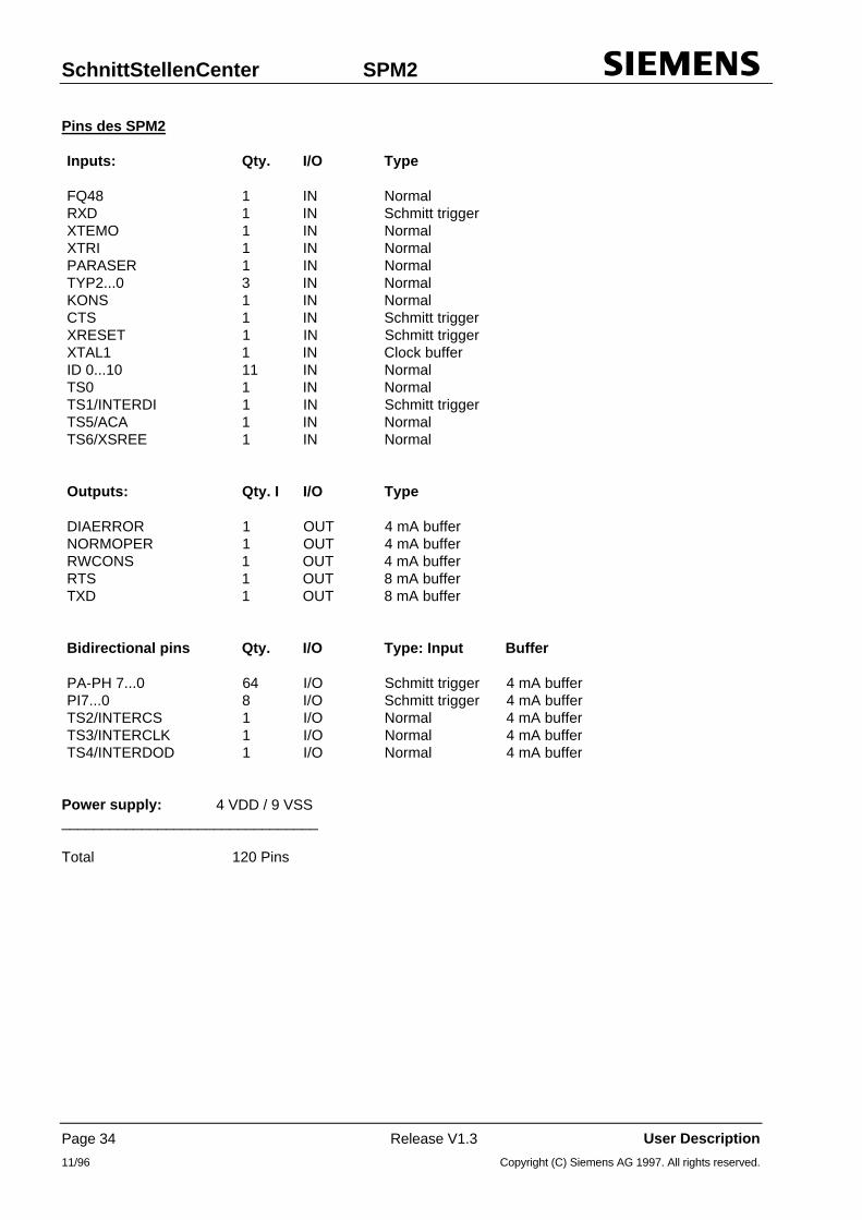
Pins des SPM2
Inputs: Qty. I/O Type
FQ48 1 IN NormalRXD 1 IN Schmitt triggerXTEMO 1 IN NormalXTRI 1 IN NormalPARASER 1 IN NormalTYP2...0 3 IN NormalKONS 1 IN NormalCTS 1 IN Schmitt triggerXRESET 1 IN Schmitt triggerXTAL1 1 IN Clock bufferID 0...10 11 IN NormalTS0 1 IN NormalTS1/INTERDI 1 IN Schmitt triggerTS5/ACA 1 IN NormalTS6/XSREE 1 IN Normal
Outputs: Qty. I I/O Type
DIAERROR 1 OUT 4 mA bufferNORMOPER 1 OUT 4 mA bufferRWCONS 1 OUT 4 mA bufferRTS 1 OUT 8 mA bufferTXD 1 OUT 8 mA buffer
Bidirectional pins Qty. I/O Type: Input Buffer
PA-PH 7...0 64 I/O Schmitt trigger 4 mA bufferPI7...0 8 I/O Schmitt trigger 4 mA bufferTS2/INTERCS 1 I/O Normal 4 mA bufferTS3/INTERCLK 1 I/O Normal 4 mA bufferTS4/INTERDOD 1 I/O Normal 4 mA buffer
Power supply: 4 VDD / 9 VSS________________________________
Total 120 Pins
SPM2 SchnittStellenCenter
User Description Release V1.3 Page 35
Copyright (C) Siemens AG 1997. All rights reserved. 11/96
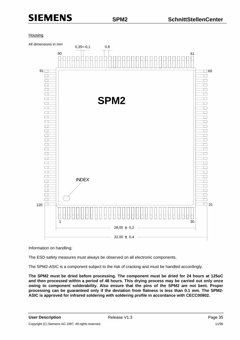
Housing
SPM2
90 61
60
31
1 30
120
91
0,35+-0,1 0,8
28,00 0,2
32,00 0,4
All dimensions in mm
INDEX
Information on handling:
The ESD safety measures must always be observed on all electronic components.
The SPM2-ASIC is a component subject to the risk of cracking and must be handled accordingly.
The SPM2 must be dried before process ing. The component must be dried for 24 hours at 125oCand then processed wit hin a period of 48 hours. This drying pro cess may be carried out only onceowing to component sold erability. Also ensure that the pins of the SPM2 are not bent. Properprocess ing can be gu aranteed only if the deviation from flatn ess is less than 0.1 mm. The SPM2-ASIC is approved for infrared soldering with soldering profile in accordance with CECC00802.

SchnittStellenCenter SPM2
Page 36 Release V1.3 User Description
11/96 Copyright (C) Siemens AG 1997. All rights reserved.
7 Timings
7.1 EEPROM
EEPROM READ cycle Op code 10 (example address 000 000b)
Start-bit
1 2 1 2 3 4 5 6
1
Data2-bit Op code 6-bit address
INTERCLK
INTERDOD
INTERCS
INTERDI
Start-bit
1 2 1 2 3 4 5 6
1
Data2-bit Op code 6-bit address
INTERCLK
INTERDOD
INTERCS
INTERDI
EEPROM READ cycle Op code 10 (example address 000 001b)
1 min. 2µs The controller switches the signals to the pins with the trailing edge

SPM2 SchnittStellenCenter
User Description Release V1.3 Page 37
Copyright (C) Siemens AG 1997. All rights reserved. 11/96
EEPROM ERASE/WRITE cycleE
EP
RO
M E
RA
SE
/WR
ITE
cyc
le
Sta
rt-
bit
1
2
1
2
3
4
5
6
1
2-b
it O
p c
od
e
6
-bit
ad
dre
ss
00
1
10
00
0
INT
ER
CLK
INT
ER
DO
D
INT
ER
CS
1
INT
ER
CLK
INT
ER
DO
D
INT
ER
CS
INT
ER
DI
EE
PR
OM
WR
ITE
cyc
le
3*S
C
Pro
gra
mm
ing
time
(
ma
x. 1
0m
s)
Wa
itin
g fo
r R
EA
DY R
EA
DY
Th
e W
rite
cyc
le fo
llow
s w
itho
ut i
nte
rru
ptio
n.
1m
in.
2us
Th
e c
on
tro
ller
switc
he
s th
e s
ign
als
to
th
e p
ins
with
th
e t
raili
ng
ed
ge.
D15
D14
D13
D0
Sta
rt-
bit
1
2
1
2
3
4
5
6
2-b
it O
p c
od
e
6
-bit
ad
dre
ss
01
000
00
0D
ata
SchnittStellenCenter SPM2
Page 38 Release V1.3 User Description
11/96 Copyright (C) Siemens AG 1997. All rights reserved.
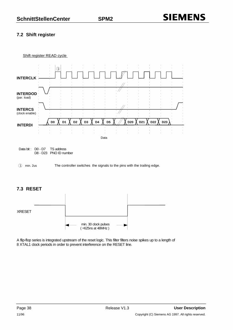
7.2 Shift register
Shift register READ cycle
1
Data
INTERCLK
INTERDOD(par. load)
INTERCS(clock enable)
INTERDID0 D1 D2 D3 D4 D5 D20 D21 D22 D23
1 min. 2us The controller switches the signals to the pins with the trailing edge.
Data bit : D0 - D7 TS address D8 - D23 PNO ID number
7.3 RESET
XRESET
min. 30 clock pulses( =625ns at 48MHz )
A flip-flop series is integrated upstream of the reset logic. This filter filters noise spikes up to a length of8 XTAL1 clock periods in order to prevent interference on the RESET line.

SPM2 SchnittStellenCenter
User Description Release V1.3 Page 39
Copyright (C) Siemens AG 1997. All rights reserved. 11/96
7.4 Consistency signal RWCONS
Write timing: The user can switch external latches transparently for instance with RWCONS in order to accept new data from the ports programmed to Output.
1 2
RWCONS
WRITE - IO(internal)
Port data
Read timing: The user can freeze external latches for instance with RWCONS in order to accept consistent data at the ports programmed to Input ("Snapshot" option).
3 4
RWCONS
READ - IO(internal)
Port data
Nr. Symbol Parameter Unit
1 RWCONSSETUP RWCONS activ to Write from MS 1 TBit*2 RWCONSHOLD RWCONS inactiv to Write from MS 1 TBit*3 DSETUP Data - Setup after RWCONS active 1 TBit*4 DHOLD Data - Hold after RWCONS inactiv 0 ns
*: 1 TBit =104µs at 9,6kBd , 1 TBit = 83ns at 12mbd

SchnittStellenCenter SPM2
Page 40 Release V1.3 User Description
11/96 Copyright (C) Siemens AG 1997. All rights reserved.
8 Address Directory
Profibus User Organization
PNOBusiness OfficeMr. VolzHaid- und Neu- Straße 776131 KarlsruheTel.: (0721) 9658-590
Technical reference partners in the interface center
Siemens AGAUT 7 B1 T2Mr. Frieß and Mr. Schmidt
Mailing address:Post Office Box 235590713 Fürth
Internal address:Würzburgerstr.12190766 Fürth
Tel.: (0911) 750 - 20722079
Fax (0911) 750 - 2100
We have a mailbox, there you can read the latest information and useful hints about our ASICs andproducts.Tel.: 0911 - 737972

SPM2 SchnittStellenCenter
User Description Release V1.3 Page 41
Copyright (C) Siemens AG 1997. All rights reserved. 11/96
9 Circuit examples
9.1 Shift registerG
1C
21
1
1 3D 2D 2D
C3/
G1
C2
1
11 3D 2D 2D
C3/
330R
TS
add
ress
BC
D c
ode
d
Bit
7B
it 6
Bit
5B
it 4
Bit
3B
it 2
Bit
1B
it 0
15K
15K
15K
15K
15K
15K
15K
15K
3K3
3K3
3K3
3K3
3K3
3K3
3K3
3K3
P5
SP
M2
INT
ER
CS
INT
ER
CL
KIN
TE
RD
OD
INT
ER
DI
XS
RE
E
330R M
1 2 15 10 11 12 13 14 3 4 5 6
1 2 15 10 11 12 13 14 3 4 5 69 7
9 7
116
117
118
115
12
0
74H
C16
5
74H
C16
5
PA
RA
SE
R
<1>
= s
er. p
aram
ete
r m
em
ory
XS
RE
E
<0>
= S
hift
regi
ster
G1
C2
1
11 3D 2D 2D
C3/
1 2 15 10 11 12 13 14 3 4 5 69 7
74H
C16
5
LOW
- b
yte
PN
O -
ID
num
ber
HIG
H -
byt
eP
NO
- I
D n
umbe
r
330R
M
PA
RA
SE
R
330R P510
0

SchnittStellenCenter SPM2
Page 42 Release V1.3 User Description
11/96 Copyright (C) Siemens AG 1997. All rights reserved.
9.2 Wiring example - EEPROM , ext. oscillator , error indicator and RESET
SP
M2
INTE
RC
LKIN
TER
CS
INTE
RD
I
117
116
118
93C
46/4
7
INTE
RD
OD
115
P5
3K3
ORG
SK
CS
D
ID
O
1K
P5
1K
M
Dia
gnos
tic L
ED
(m
ax 4
mA
)
Bus
erro
r LE
D (m
ax 4
mA
)
DIA
ER
RO
R
NO
RM
OP
ER
M P5
2 4 130
0R
GU
-U
+
EN
3
48M
Hz
615P
_U
XT
AL1
7705
RE
S
C
T
UR
EF
P5 MR
UN
/ S
TOP
+ 1
0u10
n
3K3
3K3
MX
RE
SE
T
48 47
EE
PR
OM
12
300R
P5
FO 4
820
3K3 10K
3K3 10K
3K3 10K
3K3 10K
M
300R
P5
AC
A11
9
3K3 15K M
18
XS
RE
E
330R
M120
PA
RA
SE
R
<1>
= se
r. pa
ram
eter
mem
ory
XS
RE
E
<
1> =
Shi
ft re
gist
er
PA
RA
SE
R
330R P510
0

SPM2 SchnittStellenCenter
User Description Release V1.3 Page 43
Copyright (C) Siemens AG 1997. All rights reserved. 11/96
9.3 Wiring example - PROFIBUS interface
75A
LS1
76D
1 1
2
U+
EN
1G
ND
EN
2
100K 100K
2P5
2M
68n
2P5
2M
680
R
1K
2
IN U-
U+ IN U-
HC
PL7
101
U+U-
U+
68n
68n
EN
2M
P5
P5
680
R
1K2
OU
TEN
680R
300R
680
R
HC
PL0
601
2P5
&2
3
74H
C13
230
0R
U+ IN U-
300
R
68n
68n
680
R
OU
T
EN
U-
U+
20K
M
M
HC
PL7
101
2P5
2M
300
RM
CT
S
RT
S
TX
D
RX
D
Imp
orta
nt:
elec
trica
l iso
latio
n to
bus
P5
an
d 2
P5
1 4 2D
river
sel
ect
:D
iffe
ren
tial v
olta
ge >
2V
1 2 3 4 5 6 7 8 9
Lay
out
:lin
es m
ust
be k
ept
as s
hor
t as
pos
sibl
e.
M
A-li
ne
B-li
ne
RT
S
2M
2P
5
6 7
12538
1M
2.2
.. 2
2nF
500
V
Sh
ield

SchnittStellenCenter SPM2
Page 44 Release V1.3 User Description
11/96 Copyright (C) Siemens AG 1997. All rights reserved.
10 Bus connection
The bus can be connected using the following standard connectors, amongst others, in accordance withPROFIBUS-DP Standard:
MLFB-No. Notes Colour of the connector housing6ES7 972 - 0BA00 - 0XA0 without PG gland anthracite6ES7 972 - 0BB00 - 0XA0 with PG gland anthracite
Dimension drawings:
L2 bus connector: 6ES7 972 - 0B00 - 0XA0

SPM2 SchnittStellenCenter
User Description Release V1.3 Page 45
Copyright (C) Siemens AG 1997. All rights reserved. 11/96
L2 bus connector: 6ES7 972 - 0BB00 - 0XA0
The slide switch on the rear side of the bus connector must be set to position „ON“ in order to connect thebus terminating resistor.
Lines A and B of the incoming and outgoing bus cable must each be connected via separate screw-typeterminals.


Siemens AGBereich AutomatisierungstechnikKombinationstechnik Siemens AG
Postfach 23 55, D-90713 Fürth Subject to change without prior notice
SIEMENS Aktiengesellschaft Printed in the Fed. Rep. of GermanyBestell-Nr. 6ES7 195-0BB00-8BA0