slua963a | ti.com - semiconductor company | ti.com
TRANSCRIPT

1SLUA963A–November 2019–Revised June 2020Submit Documentation Feedback
Copyright © 2019–2020, Texas Instruments Incorporated
HEV/EV Traction Inverter Design Guide Using Isolated IGBT and SiC GateDrivers
Application ReportSLUA963A–November 2019–Revised June 2020
HEV/EV Traction Inverter Design Guide Using IsolatedIGBT and SiC Gate Drivers
Audrey Dearien
ABSTRACTThis document describes how to design a HEV/EV traction inverter drive system using the advantages ofTI’s isolated gate drivers diagnostic and protection features.
Contents1 Introduction ................................................................................................................... 12 HEV/EV Overview ........................................................................................................... 2
2.1 HEV/EV Architectures .............................................................................................. 22.2 HEV/EV Traction Inverter System Architecture ................................................................. 42.3 HEV/EV Traction Inverter System Performance Impact ...................................................... 7
3 Design of HEV/EV Traction Inverter Drive Stage........................................................................ 83.1 Introduction to UCC217xx-Q1..................................................................................... 83.2 Designing a Traction Inverter Drive System Using UCC217xx-Q1 .......................................... 93.3 Description of Protection Features ............................................................................... 93.4 Protection Features of UCC217xx-Q1 ........................................................................... 93.5 UCC217xx-Q1 Protection and Monitoring Features Descriptions .......................................... 113.6 Introduction to UCC5870-Q1 .................................................................................... 193.7 Designing a Traction Inverter Drive System Using UCC5870-Q1 .......................................... 203.8 Description of Protection Features .............................................................................. 203.9 Protection Features of UCC5870-Q1 ........................................................................... 213.10 UCC5870-Q1 Protection and Monitoring Features Descriptions............................................ 22
4 Isolated Bias Supply Architecture ........................................................................................ 325 Summary .................................................................................................................... 346 References .................................................................................................................. 34
1 IntroductionIntelligent means of vehicle monitoring and protection are necessary due to the full electrification ofvehicles and the stringent safety requirements that vehicle manufacturers are held to. The electronicssystems and components must remain functional throughout the vehicle's lifetime in order to maintain safeoperation. The traction inverter is vital to the drive system and includes protection and monitoring auxiliarycircuits to prevent system-level failure modes such as over- and under-torque, unintentional motorcommutation, or motor shutdown. This design guide reviews HEV/EV architectures, the failure modes ofthe traction inverter system, and how the gate driver and surrounding circuits can be used to enhance thereliability of the system. Texas Instruments’ UCC217xx-Q1 family of reinforced isolated gate drivers haveintegrated protection and monitoring features that simplify the design of high-power traction invertersystems. This family of drivers is developed under the TI Functional Safety Quality-Managed process.Such features include fast over-current protection or short-circuit protection, isolated temperature andvoltage sensing, and under voltage lockout. Additionally, the advanced feature UCC5870-Q1 basicisolated gate driver includes integrated SPI-programmable diagnostic, protection and monitoring functionsand is developed under the Functional Safety-Compliant TI process. For more information regarding thecategories of TI's safety chips, visit TI's Functional Safety web page.

Transmission
Electric Motor
3-phase inverter /
rectifier
Battery
Fuel
ICE
Generator
Transmission
Electric Motor
3-phase inverter /
rectifier
Battery
Fuel
Mechanical Coupling
ICE
Transmission
Electric Motor
3-phase inverter /
rectifier
Battery
Fuel
Generator
Mechanical Coupling
ICE
(a) (b) (c)
HEV/EV Overview www.ti.com
2 SLUA963A–November 2019–Revised June 2020Submit Documentation Feedback
Copyright © 2019–2020, Texas Instruments Incorporated
HEV/EV Traction Inverter Design Guide Using Isolated IGBT and SiC GateDrivers
2 HEV/EV OverviewThis section describes the key components of an HEV/EV automotive powertrain system.
2.1 HEV/EV ArchitecturesThe electrification of vehicles has revolutionized the transportation industry and has resulted intechnological advancements in both the automotive and semiconductor industries. Electrified vehiclesincluding both hybrid electric (HEV) and full electric (EV) vehicles consist of various power electronicssystems for regulating power from the grid, managing the battery storage element, and ultimately drivingthe vehicle. Electric motors are used to drive the wheels of the vehicle or to act as a generator to transfermechanical energy into electric energy to store in the battery. HEVs use a combination of electric motorsand generators, used as a low-power starter and alternator or to fully drive the vehicle, along with theinternal combustion engine (ICE) typically used as the primary source of the vehicle's motion. The EV, onthe other hand, utilizes electric motors as the primary source of vehicle motion as well as for regeneration.
The main HEV architectures are series, parallel and combination of series and parallel, shown in Figure 1.In the series configuration (a), the ICE is indirectly tied to the transmission through the electric motor. Thepower electronics three-phase drive derives power from the ICE through the generator as well as from thebattery. In this architecture, the ICE is optimized for a certain range of speed allowing for minimized sizeand increased efficiency. This is the simplest HEV architecture with regards to mechanical complexitysince there is no coupling of mechanical energy.
The parallel HEV configuration (b) utilizes a combination of the ICE and electric motor mechanicallycoupled. The electric drive is primarily used as a low-power starter and alternator in this architecture, andis thus lower power. The efficiency of the ICE is lower due to the larger operating range but the size of theelectric motor is minimized because it does not need to provide as much power as the ICE.
The series/parallel configuration (c) combines the two previous methods to achieve better efficiency.Mechanical coupling is performed by a planetary gear and the ICE and electric drives combine the tractionpower. In this case, the electric motor and ICE can be designed to operate within specified output rangesto improve their efficiency.
In each case, the three phase inverter is used to drive the electric motor. The inverter design varies basedon the power output requirements which depends on architecture. The proper control of the inverterdirectly impacts the motor's efficiency and the overall efficiency of the vehicle.
Figure 1. HEV Architectures

Battery
EM EM
EM
Differential
Battery
EM EM
EM EM
Battery
EM
Differential
EM
Differential
(a) (b) (c)
www.ti.com HEV/EV Overview
3SLUA963A–November 2019–Revised June 2020Submit Documentation Feedback
Copyright © 2019–2020, Texas Instruments Incorporated
HEV/EV Traction Inverter Design Guide Using Isolated IGBT and SiC GateDrivers
The pure electric vehicle, on the other hand, does not have an ICE and relies solely on the energy of thebattery. Some different configurations of electric motor is shown in Figure 2. Similar to the HEV, eacharchitecture results in different power requirements for the inverter. The electric motor may be directly tiedto the wheel as shown in configurations (a) and (b) or tied to the wheel through a differential as shown in(a) and (c). Direct in-wheel drives has the benefit of simplicity and high efficiency with low maintenance,but must typically be larger in size due to low-speed requirements. The differential drive allows for highpower density such that the motor can operate at a high RPM while the differential provides a fixed gearratio. The drawback is that the mechanical gears require maintenance and has transmission loss.
High-voltage Li-ion batteries are commonly used as the energy storage unit to provide the maximumamount of capacity, minimal weight, and highest efficiency. With current technology, including variousbattery chemistries and power electronics efficiency, EVs still have limited range compared to HEV andplug-in HEVs. High performance EVs rely on increased power level of the traction inverter, minimization ofthe electronics' size, and complex controls based on sensed signals.
By increasing the efficiency and robustness of the inverter comes the increase of overall vehicle efficiency.The gate drivers makes an impact by providing the driving force behind each power switch in the inverter,as well as protection and monitoring to reduce the likelihood of failure.
Figure 2. EV Architectures
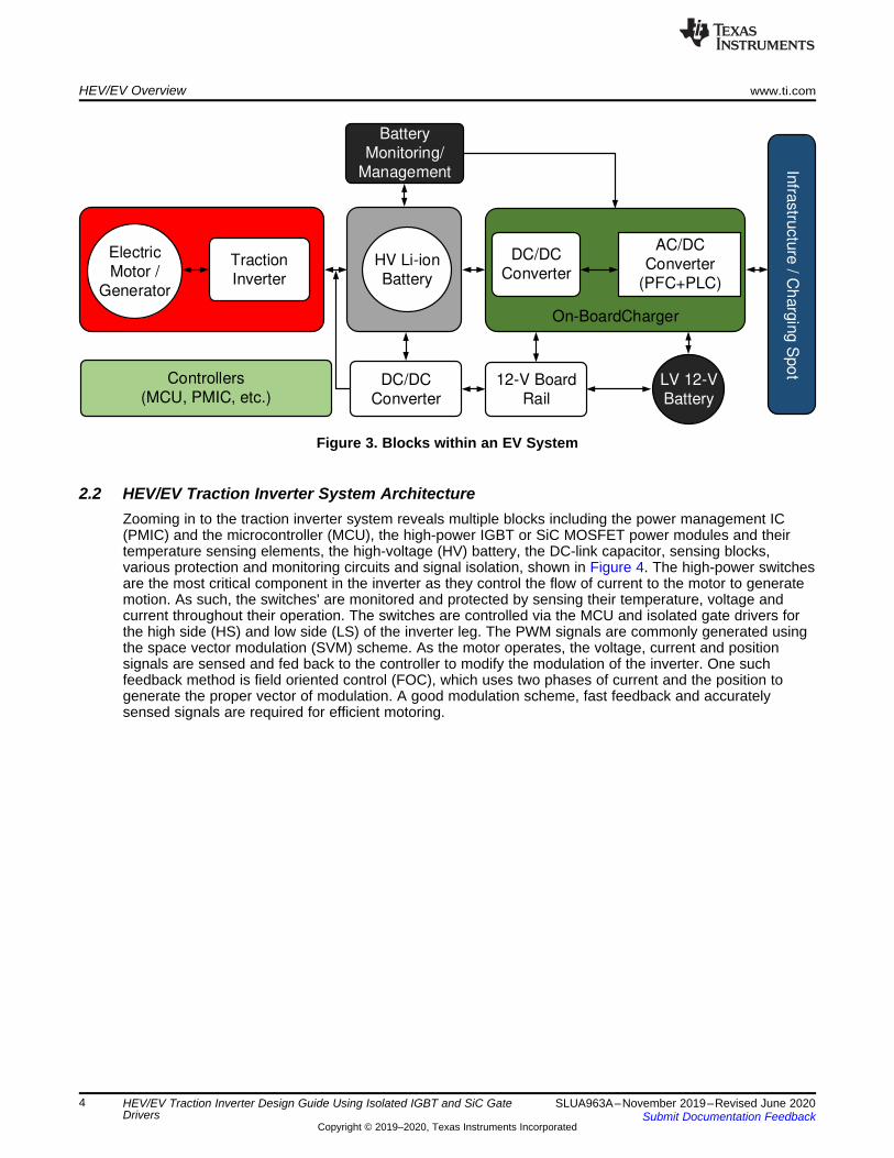
The key blocks of an EV powertrain system are the electric motor, the traction inverter drive, the DC/DCconverter, the Li-ion battery, the AC/DC grid-tied on-board charger (OBC), and controllers (MCU andPMIC), as shown in Figure 3. The traction inverter system, highlighted in red, is described in detail in thefollowing sections. This system alone incorporates many of the protection and monitoring features utilizedto achieve high safety levels.
Electric
Motor /
Generator
Traction
InverterHV Li-ion
Battery
DC/DC
Converter
12-V Board
Rail
LV 12-V
Battery
AC/DC
Converter
(PFC+PLC)
Battery
Monitoring/
Management Infra
stru
ctu
re / C
harg
ing S
po
t
Controllers
(MCU, PMIC, etc.)
On-BoardCharger
DC/DC
Converter
HEV/EV Overview www.ti.com
4 SLUA963A–November 2019–Revised June 2020Submit Documentation Feedback
Copyright © 2019–2020, Texas Instruments Incorporated
HEV/EV Traction Inverter Design Guide Using Isolated IGBT and SiC GateDrivers
Figure 3. Blocks within an EV System
2.2 HEV/EV Traction Inverter System ArchitectureZooming in to the traction inverter system reveals multiple blocks including the power management IC(PMIC) and the microcontroller (MCU), the high-power IGBT or SiC MOSFET power modules and theirtemperature sensing elements, the high-voltage (HV) battery, the DC-link capacitor, sensing blocks,various protection and monitoring circuits and signal isolation, shown in Figure 4. The high-power switchesare the most critical component in the inverter as they control the flow of current to the motor to generatemotion. As such, the switches' are monitored and protected by sensing their temperature, voltage andcurrent throughout their operation. The switches are controlled via the MCU and isolated gate drivers forthe high side (HS) and low side (LS) of the inverter leg. The PWM signals are commonly generated usingthe space vector modulation (SVM) scheme. As the motor operates, the voltage, current and positionsignals are sensed and fed back to the controller to modify the modulation of the inverter. One suchfeedback method is field oriented control (FOC), which uses two phases of current and the position togenerate the proper vector of modulation. A good modulation scheme, fast feedback and accuratelysensed signals are required for efficient motoring.

M
Pos.
Position
Sensing
Temperature
Sensing
DC Bus
Voltage
Sensing
HS DriverHS DriverIsolated HS
Driver
HS DriverHS DriverIsolated LS
Driver
MCU
PMICIsolated Bias
Supply(s)
Signal
Isolation
Temperature
SensingTemperature
Sensing
Isolation Barrier
Current
Sensing
Shoot-
through
protection
and RESET
control
HV Battery
Voltage
Sensing
CAN Bus
IGBT
Modules
VCE
Monitoring
Short-Circuit
Monitoring/
Protection
Signal
Isolation
DC-link
Capacitor
www.ti.com HEV/EV Overview
5SLUA963A–November 2019–Revised June 2020Submit Documentation Feedback
Copyright © 2019–2020, Texas Instruments Incorporated
HEV/EV Traction Inverter Design Guide Using Isolated IGBT and SiC GateDrivers
Figure 4. High-Voltage Traction Inverter Block Diagram
A closer look at the inverter, shown in Figure 5, reveals six total semiconductor power switching deviceswith a gate driver to amplify the PWM signal from the MCU. The three legs of the inverter convert the DCbattery voltage into three phases of AC voltage and current to drive the motor. Two current measurementsand a position measurement are fed back to the MCU for FOC which utilizes mathematicaltransformations to generate the proper signals for the six switches to control the output voltages at phasesA, B and C.

VDC+
S1
S2
S3
S4
S5
S6
A
B
C C
B
A
Driver Driver Driver
VDC-
MCU
Driver Driver DriverVoltage / current /
position
MCDC
VGE,S1
VGE,S6
VGE,S3
VGE,S4
VGE,S5
VGE,S2
HEV/EV Overview www.ti.com
6 SLUA963A–November 2019–Revised June 2020Submit Documentation Feedback
Copyright © 2019–2020, Texas Instruments Incorporated
HEV/EV Traction Inverter Design Guide Using Isolated IGBT and SiC GateDrivers
Figure 5. Three-Phase Two-Level Inverter Using IGBTs
In vector modulation, eight total states are available where two are zero vectors and the rest are activevectors used to apply the necessary voltage to the motor to generate the proper amount of torque. Table 1shows the states where switch pairs S1 and S6, S3 and S4, and S5 and S2 are complementary to oneanother.
Table 1. Space Vector Modulation States
Vector S1 S2 S3 S4 S5 S6 VAB VBC VCA VectorMode
{000} OFF ON OFF ON OFF ON 0 0 0 Zero{100} ON ON OFF ON OFF OFF +VDC 0 -VDC Active{100} ON ON ON OFF OFF OFF 0 +VDC -VDC Active{010} OFF ON ON OFF OFF ON -VDC +VDC 0 Active{011} OFF OFF ON OFF ON ON -VDC 0 +VDC Active{001} OFF OFF OFF ON ON ON 0 -VDC +VDC Active{101} ON OFF OFF ON ON OFF +VDC -VDC 0 Active{111} ON OFF ON OFF ON OFF 0 0 0 Zero
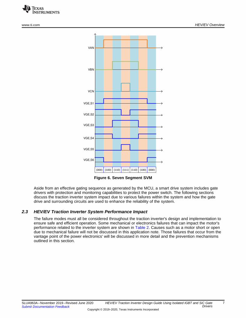
There are various methods of implementing SVM. Tradeoffs between the SVM methods include reductionof switching losses, bus voltage maximum utilization, reduced harmonic content, while still achievingprecise control. One such method is seven segment SVM, which is beneficial to produce a voltagewaveform with low harmonics, and thus less distortion when driving the motor. The gating sequence isshown in Figure 6. A single skipped or extra gate signal as a result of an MCU control error or gate driverlatched output as a result of a failure could result in inverter output distortion. Overlap of complementaryswitches in a phase leg could result in shoot through, and must always be avoided. As shown, thecommutation of the motor is dependent on very specific gating sequences. Thus, it would be very difficultto unintentionally commutate the motor with a one-off gate driver failure.
VBN
VAN
VCN
VGE,S1
VGE,S6
VGE,S3
VGE,S4
VGE,S5
VGE,S2
{000} {100} {110} {110} {100} {000}{111}
www.ti.com HEV/EV Overview
7SLUA963A–November 2019–Revised June 2020Submit Documentation Feedback
Copyright © 2019–2020, Texas Instruments Incorporated
HEV/EV Traction Inverter Design Guide Using Isolated IGBT and SiC GateDrivers
Figure 6. Seven Segment SVM
Aside from an effective gating sequence as generated by the MCU, a smart drive system includes gatedrivers with protection and monitoring capabilities to protect the power switch. The following sectionsdiscuss the traction inverter system impact due to various failures within the system and how the gatedrive and surrounding circuits are used to enhance the reliability of the system.
2.3 HEV/EV Traction Inverter System Performance ImpactThe failure modes must all be considered throughout the traction inverter's design and implementation toensure safe and efficient operation. Some mechanical or electronics failures that can impact the motor'sperformance related to the inverter system are shown in Table 2. Causes such as a motor short or opendue to mechanical failure will not be discussed in this application note. Those failures that occur from thevantage point of the power electronics' will be discussed in more detail and the prevention mechanismsoutlined in this section.

Design of HEV/EV Traction Inverter Drive Stage www.ti.com
8 SLUA963A–November 2019–Revised June 2020Submit Documentation Feedback
Copyright © 2019–2020, Texas Instruments Incorporated
HEV/EV Traction Inverter Design Guide Using Isolated IGBT and SiC GateDrivers
Table 2. Traction Inverter System Event Examples
TRACTIONINVERTER
SYSTEM IMPACTMECHANICAL CAUSE ELECTRONICS
CAUSE PREVENTION MECHANISM
Under torque Coil short or open
IGBT short or open IGBT protectionGate driverdamaged
Self-test and diagnosticsGate driver output
latchedGate driver incorrect
logicIsolation Failure
MCU failure MCU watchdogPMIC failure PMIC monitor
Sensor failure Redundant sensing
Over torque N/AMCU failure MCU watchdog
Sensor failure Redundant sensingUnintended motor
commutation N/A MCU failure MCU watchdog
Unintended motorshutdown / no
outputCoil short or open
IGBT short or open IGBT protectionDC bus failure Voltage monitorMCU failure MCU watchdogPMIC failure PMIC monitor
The voltage applied to the three windings of the motor, as previously discussed, determine the speed andtorque of the motor. Disturbances can occur due to a variety of events. The power switching devices in theinverter, referred to as the IGBTs from this point on, may become shorted or open due to a mechanicalfailure, over-heating, etc. The gate driver itself could be a source for failure if it is damaged due to over-temperature or mechanical reasons, has a latched output, receives an incorrect signal from the MCU, orhas experienced isolation barrier failure. To cover a variety of potential failures, the gate driver andauxiliary circuits are used to monitor the power switch for short circuit, proper gate voltage and othersignals to protect the IGBTs and gate drivers. Additionally, circuitry is included to perform self-tests oncritical functions in the case of a latent failure which occurs after a cycle of operation. Aside from the gatedriver circuits, the MCU or PMIC should also have redundant monitoring circuits to prevent controllerfailure or supply failure.
The following sections introduce the UCC217xx-Q1 and the UCC5870-Q1 drivers, their integratedprotection and diagnostic functions, and how they simplify the design of the traction inverter system.External circuits are also described, when necessary, to assist in performing self-tests and diagnostics.
3 Design of HEV/EV Traction Inverter Drive StageThis section will discuss how to design the HEV/EV traction inverter system using UCC217xx-Q1 andUCC5870-Q1 devices to provide the protection and diagnostics necessary for reliable operation.
3.1 Introduction to UCC217xx-Q1The UCC21732-Q1 is a galvanic isolated single channel gate drivers designed for up to 1700V SiCMOSFETs and IGBTs with advanced protection features, best-in-class dynamic performance androbustness. UCC21732-Q1 has up to ±10-A peak source and sink current. The input side is isolated fromthe output side with SiO2 capacitive isolation technology, supporting up to 1.5-kVRMS working voltage,12.8-kVPK surge immunity with longer than 40 years Isolation barrier life, as well as providing low part-to-part skew, and >150V/ns common mode noise immunity (CMTI). The UCC217xx-Q1 family of devicesinclude the state-of-art protection features, such as fast overcurrent and short circuit detection, shunt

Legend
VDD
UVLO
OCP
Logic
Analog-2-
PWM
PWM
Input
VCC
UVLO
10
CLMPE
OUTH
OUTL
VDD
COM
VEE
OC
AIN
IN+
IN-
VCC
GND
RDY
nFLT
nRST/EN
APWM
2-Level +
Soft
Turn-off
Miller
clamp
control
PWM+Shoot-
through
protection
Fault
DecodeDEMOD
DEMODPWM
Driver
Output
Stage
Short
Circuit
Clamping
Fault
Encode
Secondary
Logic
To secondary side driver supply inputs
OVLO
Isolation
Barrier
TEST
Miller
Clamp
3 x Power
Stage
To high-side dr iver
M
Pos.
Motor
position
Gate-Source/
Emitter
Monitoring
Digital
Isolator(s)
VGE_MON
MCU
PMIC
CAN Bus
PWM+,
PWM-
System interrupts
(nFLT, RDY, VGE_MON)
APWM
12V Battery
V_IOV_Core
To VCC
TEST
TEST
VGE_TEST
OC_TEST
AIN_TEST
UVLO_TEST
OVLO_TEST
TEST
To AIN
VGE_MON
VGE_TEST
OC_TEST
AIN_TEST
AIN_TEST
OC_TEST
VGE_TEST
VGE_MON
TEST
VDC
Sensing
Phase
Voltage
Sensing
Current
Sensing
System Test
(VGE_TEST, OC_TEST,
AIN_TEST, UV_TEST, OV_TEST)
PWM-
RDY
nFLT
APWM
nRST/ENSystem Reset/Enable
(nRST/EN)
ProtectionDiagnosticsDriver
FunctionSelf-Test
11
15
9
12
13
14
16 1
2
8
7
6
4
3
5
From
PMIC
MOD
MOD
MOD DEMOD
OVLO_MON
UVLO_TEST
OVLO_TEST
OVLO_MON
UVLO_TEST
From isolated
supply
To OC
OVLO_TEST HV Battery
DC-link
Capaci tor
Primary
Logic
Digital
Isolator(s)
Isolated Bias
Supply
UCC21732-Q1
To MCU
www.ti.com Design of HEV/EV Traction Inverter Drive Stage
9SLUA963A–November 2019–Revised June 2020Submit Documentation Feedback
Copyright © 2019–2020, Texas Instruments Incorporated
HEV/EV Traction Inverter Design Guide Using Isolated IGBT and SiC GateDrivers
current sensing support, fault reporting, active miller clamp, input and output side power supply UVLO tooptimize SiC and IGBT switching behavior and robustness. The isolated analog to PWM sensor can beutilized for easier temperature or voltage sensing, further increasing the drivers' versatility and simplifyingthe system design effort, size and cost. The benefits of these circuits are given below, along with auxiliarycircuitry to enhance system-level reliability.
3.2 Designing a Traction Inverter Drive System Using UCC217xx-Q1The UCC21732-Q1 is shown in Figure 7 along with the various monitoring and protection blocks requiredin the inverter system. Four categories are used to describe the various blocks: Self-Test, Diagnostics,Protection and Driver Function. Self-Test blocks signify the circuits used to ensure another critical block isfunctioning properly. The Diagnostic blocks are used to feed back critical information to the MCU todetermine monitor the power stage performance and/or behavior. The Protection blocks are used toprevent IGBT failure. Finally the Driver Function blocks include the basic gate driver function.
Figure 7. Block Diagram of a Traction Inverter System with UCC217xx-Q1
3.3 Description of Protection FeaturesThis section describes the UCC217xx-Q1 integrated protection and diagnostic features and non-integratedfeatures that are beneficial for reliable traction inverter system operation.
3.4 Protection Features of UCC217xx-Q1The system impact of various failures are shown as given in Table 2 may be prevented using integratedand auxiliary circuits around the gate driver. Table 3 shows these system impacts and potential failuresalong with the integrated and auxiliary circuits of the gate driver circuitry that can be used to prevent them.
The potential failure location(s) within the system block are as shown in Figure 8, classified as (F1) PMICfailure, (F2) MCU failure, (F3) Driver failure, or (F4) Motor/Mechanical failure.

Design of HEV/EV Traction Inverter Drive Stage www.ti.com
10 SLUA963A–November 2019–Revised June 2020Submit Documentation Feedback
Copyright © 2019–2020, Texas Instruments Incorporated
HEV/EV Traction Inverter Design Guide Using Isolated IGBT and SiC GateDrivers
Table 3. Protection and Diagnostic Features Using UCC217xx-Q1
System impactAssociated
driver and/orinverterfailures
Potential failure location(s) UCC217xx-Q1 integratedfeatures
Externalcircuit
features
Torque disturbance
Over or undervoltage of
driver powersupply
F1 UVLO + interrupt signal OVLO +interrupt signal
Unintended commutationGate driverpulse width
skewF2 or F3 Low-delay capacitive isolation
barrier and proven process N/A
Unintended motor shutdown /Torque disturbance
Power switchshort circuit F2 or F4 DESAT/OC detection and
interrupt
DESAT(UCC21750) or
OC(UCC21732/10
) self-testUVLO/OVLO
self-test
Unintended motor shutdown /Torque disturbance
Gate shortedto ground or
VDDF2 or F3 N/A
VGEmonitoring and
compare toPWM withinterrupt
Unintended motor shutdown
Power switchshoot-throughdue to false
gate signal ordv/dt-induced
current
F2Anti-shoot-through logic and
Miller clamp (internal orexternal
N/A
Torque disturbance Power switchover-voltage F2 Two-level turn-off and/or soft
turn-offVCE/VDSmonitoring
Torque disturbancePower switch
over-temperature
F1, F2, or F4 Integrated isolated sensingwith integrated bias current N/A
Torque disturbancePower switch
gate oxidebreakdown
F2 or F4 Short circuit clamping to VDD N/A
Torque disturbance
Power switchfalse turn-onwhen input
power isfloating
F1 or F2 Active pulldown N/A
Torque disturbance /Unintended motor shutdown
Power systemDC bus
over/undervoltage
F1 or F4 Integrated isolated sensing N/A

VDD UVLO
Temperature Monitoring
PWM Input + Anti Shoot Through
VCC UVLO
SC Protection
PWM+
PWM Driver
Driver Output
Short Circuit Clamping
OVLO
Isolation Barrier
M
Pos.
Gate-Source/Emitter
Monitoring
VGE Monitoring
MCU
PMIC
12V BatteryVGE Test
OC Test
AIN Test
UVLO TestOVLO Test
VGE Monitoring
VGE Test
OC Test
AIN Test
AIN Test
OC Test
VGE Test
VGE Monitoring
Sensors
PWM-
RDY
nFLT
APWM
nRST/EN
OVLO Monitor
UVLO TestOVLO Test
OVLO Monitor
UVLO Test
OVLO Test
HV Battery
DC-link Capacitor
Digital Isolator(s)
Isolated Bias Supply
UCC21732-Q1
V_IO
Reset and Enable
Voltage Monitor Interrupt
Short Circuit Interrupt
V_Core
PWM
External Interrupt and
GPIO
Multichannel ADC
x
F1
x
F3
x
F2
x
F4
www.ti.com Design of HEV/EV Traction Inverter Drive Stage
11SLUA963A–November 2019–Revised June 2020Submit Documentation Feedback
Copyright © 2019–2020, Texas Instruments Incorporated
HEV/EV Traction Inverter Design Guide Using Isolated IGBT and SiC GateDrivers
Figure 8. Possible Traction Inverter System-Level Failures and Prevention Circuits Using UCC21732-Q1
3.5 UCC217xx-Q1 Protection and Monitoring Features DescriptionsThis section describes the implementation of monitoring and protection circuits using UCC217xx-Q1.
3.5.1 Primary and Secondary Side UVLO and OVLOUnder and over-voltage lockout (UVLO and OVLO) are used to protect the driver IC as well as monitor thevoltage used to drive the power switch on the secondary side. UVLO is integrated into UCC217xx-Q1 forboth the primary and secondary side supplies, VCC and VDD respectively. These are used to protect thesystem in case of bias supply failures. The output is pulled low if VCC or VDD drops below the UVLOthreshold. Additionally, if there is a UVLO fault, the RDY pin will go HIGH. For VCC the threshold is 2.7 Vwith a 0.2 V band of hysteresis. The VDD UVLO threshold is 12 V, referenced to COM, with 0.8 Vhysteresis. Aside from bias failures, the VDD-side UVLO is beneficial to protect the power switch. Basedon the I-V characteristics of high-power IGBTs and SiC MOSFETs, if the device is driven at 12 V theconduction losses are smaller and early saturation of the device can be prevented. In this way, UVLO canbe useful to prevent damaging the FET due to a drop in supply voltage.

UCC217xx-Q1
OUTH
OUTL
COM
IN+
IN-
VCC
GND
PWM from MCU
VDD
+
Digital Isolator
VCC
GND
VDD2
COM
R2 C1
R3
D1
OVLO_int to MCU
RDY
UVLO_int to MCU
R1
UVLO
UVLO
Design of HEV/EV Traction Inverter Drive Stage www.ti.com
12 SLUA963A–November 2019–Revised June 2020Submit Documentation Feedback
Copyright © 2019–2020, Texas Instruments Incorporated
HEV/EV Traction Inverter Design Guide Using Isolated IGBT and SiC GateDrivers
Overvoltage lockout (OVLO) is also implemented to protect the power switch from being driven with toohigh of a voltage, outside of the device ratings, which could cause gate oxide breakdown or reducedlifetime. The driver IC should not be supplied with a voltage beyond the maximum ratings, as it may resultin driver failure and uncertain driver output state. OLVO is implemented using external circuitry to protectthe driver and power device from bias supply failure on the secondary side supply, VDD. VDD is divideddown and compared to a fixed voltage reference generated by a Zener diode. When the divided voltagedrops below the Zener voltage, the comparator output will switch and will be sent across the isolationbarrier to the MCU.
Figure 9. Integrated UVLO and External OVLO Implementation
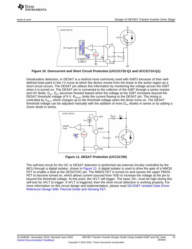
3.5.2 Over-Current (OC) and Desaturation (DESAT) DetectionOvercurrent (OC) protection (UCC21732-Q1 and UCC21710-Q1) and desaturation (DESAT) protection(UCC21750-Q1) are used to prevent a short-circuit event from destroying the power devices. Both OC andDESAT protection are available with UCC217xx variants and are integrated internally, with a few externalcomponents based on the application. The OC and DESAT protection ST (self-test) circuits may beimplemented externally and are shown below.
Integrated OC protection is shown in Figure 10. In this example, the IGBT's current is stepped down withan integrated current mirror and is output at the split emitter. The current is then measured via a shuntresistor, RShunt. The OC pin monitors the current via the voltage across RShunt and triggers the OC faultwhen the voltage surpasses the internal threshold of 0.7 V. At this time, the driver will initiate soft turn-offand/or 2-level turn-off to safely shut down the power device.
+
+
±VDESAT
COM
VDDDHV
CBLK
DESAT
DESAT
Fault
UCC21750-Q1
RDESAT
ICHG
RShunt
+
+
±VOCTH
COM
CFILT
15
0n
s
Deg
litc
h F
ilte
r
OC
OC Fault
Control Logic
UCC21732-Q1
www.ti.com Design of HEV/EV Traction Inverter Drive Stage
13SLUA963A–November 2019–Revised June 2020Submit Documentation Feedback
Copyright © 2019–2020, Texas Instruments Incorporated
HEV/EV Traction Inverter Design Guide Using Isolated IGBT and SiC GateDrivers
Figure 10. Overcurrent and Short Circuit Protection (UCC21732-Q1 and UCC21710-Q1)
Desaturation detection, or DESAT is a method most commonly used with IGBTs because of their well-defined knee point in the I-V curve at which the device moves from the linear to the active region as ashort circuit occurs. The DESAT pin utilizes this information by monitoring the voltage across the IGBTwhen it is turned on. The DESAT pin is connected to the collector of the IGBT through a series resistorand HV diode, DHV. DHV becomes forward biased when the voltage at the IGBT increases beyond theDESAT threshold voltage of 9 V. RDESAT limits the current flowing to the DESAT pin. The timing iscontrolled by CBLK, which charges up to the threshold voltage when the driver turns on. The DESATthreshold voltage can be adjusted manually with the addition of more DHV diodes in series or by adding aZener diode in series.
Figure 11. DESAT Protection (UCC21750)
The self-test circuit for the OC or DESAT detection is performed via external circuitry controlled by theMCU through a digital isolator, shown in Figure 12. A digital isolator is used to drive the gate of a NMOSFET to enable a fault at the DESAT/OC pin. The NMOS FET is turned on and causes the upper PMOSFET to become turned on, which allows current sourced from VDD to increase the voltage at the pin tobeyond the threshold voltage. At this point, the nFLT will trigger. The input, IN+, must be high during thisself-test for nFLT to trigger. If nFLT is triggered, then the short circuit detection is working properly. Formore information on this circuit design and implementation, please read SiC/IGBT Isolated Gate DriverReference Design With Thermal Diode and Sensing FET.

UCC217xx-Q1
OUTH
OUTL
COM
IN+
IN-
VCC
GND
PWM from MCU
VDD
Digital Isolator
VCC
GND
VDD2
COM
R4
DESAT_TEST from MCU
nFLT
DESAT_FLT to MCU
R3
R2
R1
UCC217xx-Q1
OUTH
OUTL
COM
IN+
IN-
VCC
GND
PWM from MCU
VDDnFLT
DESAT_FLT to MCU
DESAT
/OC
DESAT
/OC
DESAT
OC
RShunt
RShunt
Design of HEV/EV Traction Inverter Drive Stage www.ti.com
14 SLUA963A–November 2019–Revised June 2020Submit Documentation Feedback
Copyright © 2019–2020, Texas Instruments Incorporated
HEV/EV Traction Inverter Design Guide Using Isolated IGBT and SiC GateDrivers
Figure 12. DESAT/OC Detection Self-Test Circuit
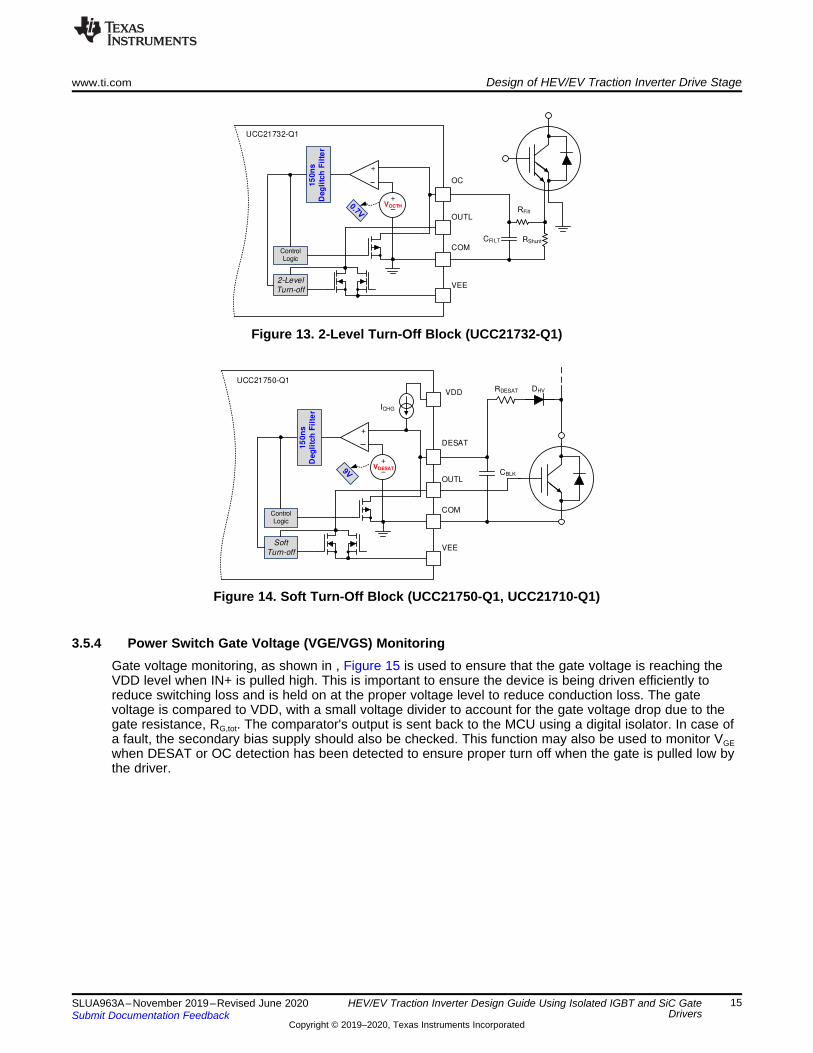
3.5.3 2-Level and Soft Turn-OffAs mentioned in the previous section, short circuit detection sends back a fault indication and triggers thedriver to turn off the IGBT or SiC MOSFET. The driver initiates either 2-level turn-off or soft turn-off tosafely shut down the IGBT or MOSFET, preventing large voltage overshoot across the device as a resultof the high current transient.
2-level turn-off, shown in Figure 13, slows down the turn-off transient by pulling the gate to a mid-levelvoltage, 9 V, during the turn-off transition to reduce the channel current flow through the device. Thissignificantly reduces the energy dissipation during the fault event. After the second voltage level is appliedfor a period of time, the driver finally pulls the gate down to VEE using a soft pull down current to transitionsmoothly to the off-state.
Soft turn-off, shown in Figure 14, uses a soft pull down current throughout the entire turn-off transition asopposed to applying a specified gate voltage. The 400 mA current causes the device to transition at aslower rate than it would with a hard turn-off, and thus reduces voltage overshoot while minimizing theamount of energy dissipation.
The inverter benefits not only to prevent the damage or destruction of the power switches, but alsoprevents high-voltages from being applied to the motor windings, which can also reduce the lifetime of themotor itself.
+
+
±VDESAT
COM
VDD DHV
CBLK
DESAT
UCC21750-Q1RDESAT
ICHG
15
0n
s
Deg
litc
h F
ilte
r
Control Logic
Soft
Turn-offVEE
OUTL
+
+
±VOCTH
COM
OC
UCC21732-Q1
15
0n
s
Deg
litc
h F
ilte
r
Control Logic
2-Level
Turn-offVEE
OUTL
RShuntCFILT
www.ti.com Design of HEV/EV Traction Inverter Drive Stage
15SLUA963A–November 2019–Revised June 2020Submit Documentation Feedback
Copyright © 2019–2020, Texas Instruments Incorporated
HEV/EV Traction Inverter Design Guide Using Isolated IGBT and SiC GateDrivers
Figure 13. 2-Level Turn-Off Block (UCC21732-Q1)
Figure 14. Soft Turn-Off Block (UCC21750-Q1, UCC21710-Q1)
3.5.4 Power Switch Gate Voltage (VGE/VGS) MonitoringGate voltage monitoring, as shown in , Figure 15 is used to ensure that the gate voltage is reaching theVDD level when IN+ is pulled high. This is important to ensure the device is being driven efficiently toreduce switching loss and is held on at the proper voltage level to reduce conduction loss. The gatevoltage is compared to VDD, with a small voltage divider to account for the gate voltage drop due to thegate resistance, RG,tot. The comparator's output is sent back to the MCU using a digital isolator. In case ofa fault, the secondary bias supply should also be checked. This function may also be used to monitor VGEwhen DESAT or OC detection has been detected to ensure proper turn off when the gate is pulled low bythe driver.

UCC217xx-Q1
OUTH
OUTL
COM
IN+
IN-
VCC
GND
PWM from MCU
VDD
+
Digital Isolator
VCC
GND
VDD2
COM
R1 C1
R2
D1
VGE_mon to MCU
RG,tot
Design of HEV/EV Traction Inverter Drive Stage www.ti.com
16 SLUA963A–November 2019–Revised June 2020Submit Documentation Feedback
Copyright © 2019–2020, Texas Instruments Incorporated
HEV/EV Traction Inverter Design Guide Using Isolated IGBT and SiC GateDrivers
Figure 15. VGE Monitoring Circuit
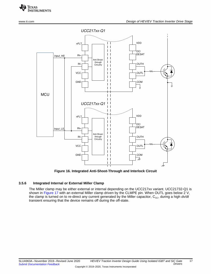
3.5.5 Power Switch Anti-Shoot-ThroughAnti-shoot through circuitry is integrated in UCC217xx to prevent IN+ and IN- from overlapping. Thisallows for two single-channel drivers to be interlocked, as shown in Figure 16, where IN+ of the upperdevice is tied to IN- of the lower device, and vise versa. This prevents the upper and lower switches fromconducting at the same time, which would result in a short circuit and device over-heating.
Anti Shoot-through Circuitry
UCC217xx-Q1
OUTH
OUTL
COM
IN+
IN-
VCC
GND
VDDnFLT
OC/
DESAT
UCC217xx-Q1
OUTH
OUTL
COM
IN+
IN-
VCC
GND
VDDnFLT
OC/
DESAT
Anti Shoot-through Circuitry
Input_HS
Input_LS
MCU
www.ti.com Design of HEV/EV Traction Inverter Drive Stage
17SLUA963A–November 2019–Revised June 2020Submit Documentation Feedback
Copyright © 2019–2020, Texas Instruments Incorporated
HEV/EV Traction Inverter Design Guide Using Isolated IGBT and SiC GateDrivers
Figure 16. Integrated Anti-Shoot-Through and Interlock Circuit
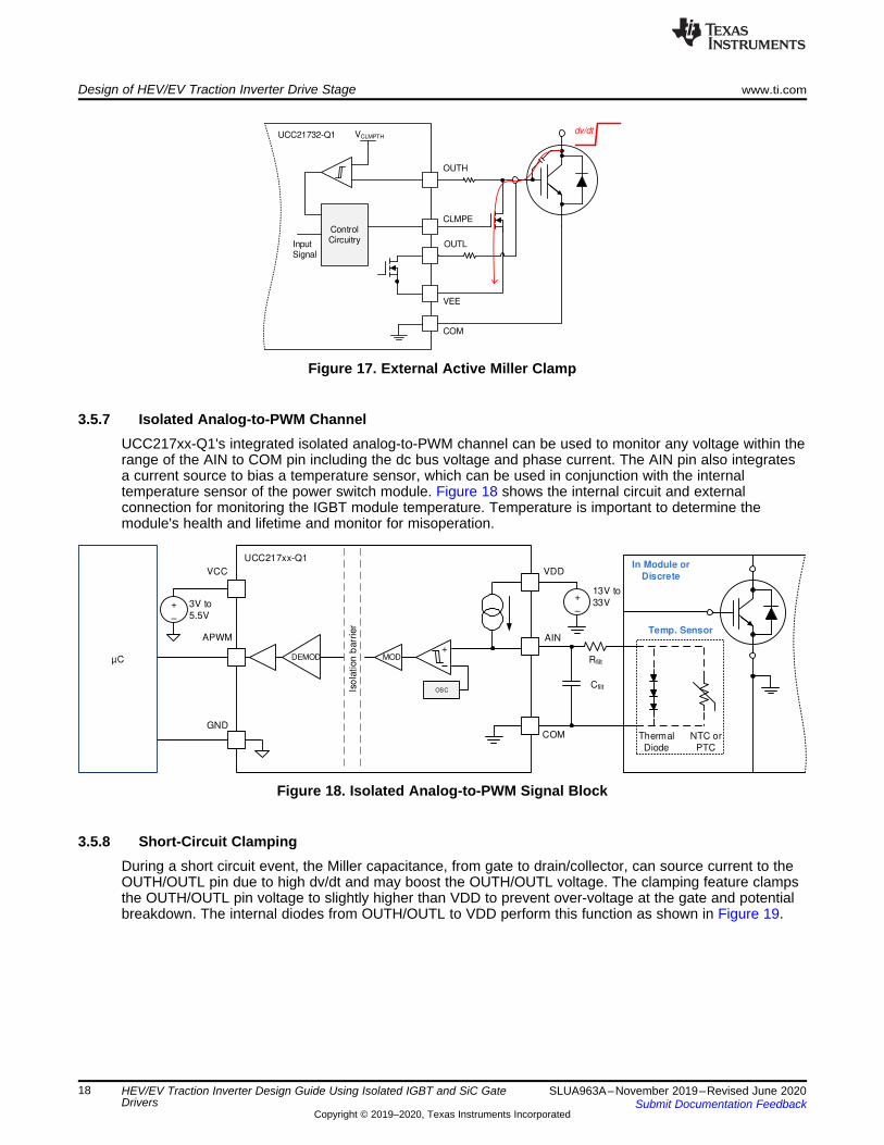
3.5.6 Integrated Internal or External Miller ClampThe Miller clamp may be either external or internal depending on the UCC217xx variant. UCC21732-Q1 isshown in Figure 17 with an external Miller clamp driven by the CLMPE pin. When OUTL goes below 2 V,the clamp is turned on to re-direct any current generated by the Miller capacitor, CGC, during a high dv/dttransient ensuring that the device remains off during the off-state.
COM
VDD
Cfilt
AIN+
OSC
MOD
In Module or
Discrete
Thermal
Diode
Iso
lation
barr
ier
NTC or
PTC
UCC217xx-Q1
DEMOD
APWM
VCC
GND
µC
+
±
3V to
5.5V
+
±
13V to
33V
Rfilt
Temp. Sensor
OUTH
COM
VEE
VCLMPTH
Control Circuitry
CLMPE
OUTL Input Signal
UCC21732-Q1dv/dt
Design of HEV/EV Traction Inverter Drive Stage www.ti.com
18 SLUA963A–November 2019–Revised June 2020Submit Documentation Feedback
Copyright © 2019–2020, Texas Instruments Incorporated
HEV/EV Traction Inverter Design Guide Using Isolated IGBT and SiC GateDrivers
Figure 17. External Active Miller Clamp
3.5.7 Isolated Analog-to-PWM ChannelUCC217xx-Q1's integrated isolated analog-to-PWM channel can be used to monitor any voltage within therange of the AIN to COM pin including the dc bus voltage and phase current. The AIN pin also integratesa current source to bias a temperature sensor, which can be used in conjunction with the internaltemperature sensor of the power switch module. Figure 18 shows the internal circuit and externalconnection for monitoring the IGBT module temperature. Temperature is important to determine themodule's health and lifetime and monitor for misoperation.
Figure 18. Isolated Analog-to-PWM Signal Block
3.5.8 Short-Circuit ClampingDuring a short circuit event, the Miller capacitance, from gate to drain/collector, can source current to theOUTH/OUTL pin due to high dv/dt and may boost the OUTH/OUTL voltage. The clamping feature clampsthe OUTH/OUTL pin voltage to slightly higher than VDD to prevent over-voltage at the gate and potentialbreakdown. The internal diodes from OUTH/OUTL to VDD perform this function as shown in Figure 19.

COM
VEE
OUTL
Control
Circuit
VDDUCC217xx-Q1
VDD
Control
Circuitry
OUTH
OUTL
D1 D2
UCC217xx-Q1
www.ti.com Design of HEV/EV Traction Inverter Drive Stage
19SLUA963A–November 2019–Revised June 2020Submit Documentation Feedback
Copyright © 2019–2020, Texas Instruments Incorporated
HEV/EV Traction Inverter Design Guide Using Isolated IGBT and SiC GateDrivers
Figure 19. Short Circuit Clamping Block
3.5.9 Active PulldownActive pulldown ensures that OUTH/OUTL is clamped to VEE while VDD is not connected. TheOUTH/OUTL pin is high-impedance when VDD is open and the pulldown feature prevents false turn onwhile the device supply is open. This is implemented as shown in Figure 20.
Figure 20. Active Pulldown Block
3.6 Introduction to UCC5870-Q1The UCC5870-Q1 is a device is a TI Functional Safety-Compliant, isolated, single-channel gate drivertargeted to drive high power SiC MOSFETs and IGBTs in EV/HEV applications. The input side is isolatedfrom the output side using SiO2 capacitive isolation technology, supporting up to 1-kVRMS workingvoltage and longer than 40 years isolation barrier life, as well as providing low part-to-part skew, and>100V/ns common mode noise immunity (CMTI).
The UCC5870-Q1 is a platform-supporting device. The flexibility of SPI programmable blanking times,deglitches, thresholds, function enables, and fault handling allow for the UCC5870-Q1 to support a widevariety of IGBT or SiC power transistors that are used across a wide variety of applications. UCC5870-Q1integrates all of the protection features required in most traction inverter applications. Additionally, the 15Agate drive capability eliminates the need for an external booster circuit, reducing overall solution size. Theintegrated Miller clamp circuit holds the gate off during transient events and can be configured to use theinternal 4A pull-down, or drive an external n-channel MOSFET. All of the protections for the powertransistor are integrated into the UCC5870-Q1. It supports DESAT and resistor-based over-currentprotection. A negative temperature coefficient power transistor temperature sensor monitor is built into thedevice to alert the host and prevent damage from over-temperature conditions in the switch. A zener-breakdown based clamping function is integrated to reduce the gate drive, and thereby the overshootenergy, when over-voltage spikes during turn-off occur due to inductive kick-back. Real-time gatemonitoring is integrated to ensure proper connection to the power transistor and alert the host to a fault inthe gate driver path.

NC
SDO
SDI
nCS
CLK
IN-
ASC_EN
IN+
nFLT1
AI5
VREF
OUTL
GND2
VBST
CLAMP
OUTH
DESAT
VREG2
VCC2
AI4
AI2
AI3
AI1
AI6
VEE2
VCC1
NC
GND1
NC
VEE2
ASC
GND1
nFLT2/DOUT
NC
VREG1
VCECLP
1
2
3
4
5
6
7
8
9
10
11
12
13
14
15
16
17
18
36
35
34
33
32
31
30
29
28
27
26
25
24
23
22
21
20
19
PWM-
PWM+
Shoot-
through
protection
VCC2
VREG2
VEE2
Monitor
Legend
ProtectionDiagnosticsDriver
FunctionSelf-Test
Output
Stage
OC/SC
2-Level /
Soft Turn-off
Miller
clamp
control
Gate
monitor
Digital Core
Digital Core
VCE
Clamp
UCC5870-Q1
ASC
Logic
Diagnostics
TEST
DESAT
VREG2
Isolated Bias
Supply
Isolation
Barrier
MCU
PMIC
CAN Bus
nCS
SDO
12V Battery
V_IOV_Core
To VCC1
SDI
CLK
PWM+
PWM-
nCS
SDO
SDI
CLK
From
PMIC
From
PMIC
ASC
ASC_ENFrom
PMIC
To MCU
To MCU
nFLT1
nFLT2 / DOUT
Miller
Clamp
3 x Power
Stage
To high-side driver
M
Pos.
Motor
position
VDC
Sensing
Phase
Voltage
Sensing
Current
Sensing
To AI2,
4, or 6
HV
Battery
DC-link
Capacitor
Thru ISO
to MCU
To secondary side driver supply inputs
To AI1,
3, or 5
From isolated supply
From isolated supply
From shunt
resistor or other
From temp
sensor or other
From shunt
resistor or other
From temp
sensor or other
HV Safety
Controller
To AI* redundant
VDC meas
Secondary ASC
or other
Secondary ASC
or other
ASC_EN
ASC
From HV
Battery
AI1,3,5
AI2,4,6
AI5,6
Diagnostics
TEST
I/O
Die to Die
Comm
Die to Die
Comm
Die to Die
Comm
Die to Die
Comm
ADC Core
VCC / VREG1 Monitor
VREG1
Design of HEV/EV Traction Inverter Drive Stage www.ti.com
20 SLUA963A–November 2019–Revised June 2020Submit Documentation Feedback
Copyright © 2019–2020, Texas Instruments Incorporated
HEV/EV Traction Inverter Design Guide Using Isolated IGBT and SiC GateDrivers
A 10-bit ADC is built-in to the UCC5870-Q1 to provide information on power switch temperature, gatedriver temperature, or any voltage that must be monitored on the secondary (high-voltage) side of the gatedriver. There are six inputs (AIx) available to measure voltages with the ADC. This is convenient toacquire information on the DC-link voltage, or for measuring the VCE/VDS voltage of the power transistorduring operation. The ADC features "center mode" operation to ensure low noise measurements, or canbe used in a traditional "edge mode" to achieve as many measurements as possible during a PWM cycle.In addition to reading back the ADC information over SPI, a DOUT function provides a feedback signalrepresenting one of the user-selected AIx voltages that can be monitored real-time on the primary side.
The UCC5870-Q1 integrates many safety diagnostics that enable designers to more easily implement anASIL rated system. There are diagnostics for all of the protection features, as well as latent fault detectionfor circuits in the gate driver IC itself. The faults are indicated using open-drain outputs, and the specificfault is easily determined using the SPI readback. In addition to all of the safety diagnostic features, the ICintegrates a primary side and secondary side "active short circuit" circuits to provide the system designerwith a secondary path to control a zero-vector state for the traction inverter in the case of motor controllerfailure.
3.7 Designing a Traction Inverter Drive System Using UCC5870-Q1The UCC5870-Q1 block diagram in the traction inverter system is shown in Figure 21. The legendspecifies the Self-Test, Diagnostics, Protection and Driver Function blocks. In comparison to theUCC217xx-Q1 family of drivers, UCC5870-Q1 integrates many more diagnostic features such thatexternal blocks are not longer required. Although this is beneficial to the system size and BOM reduction,it also results in the need for additional self-monitoring functions to ensure proper behavior. Thus,UCC5870-Q1 also has built-in monitoring functionality and user-commanded test features to ensurefunctionality of critical protection and monitoring circuits. This is done to prevent latent failures, which arethose that cannot be detected by a protection mechanism.
Figure 21. Block Diagram of a Traction Inverter System with UCC5870-Q1
3.8 Description of Protection FeaturesThis section describes the UCC5870-Q1 integrated protection and diagnostic features that are beneficialfor reliable traction inverter system operation.

www.ti.com Design of HEV/EV Traction Inverter Drive Stage
21SLUA963A–November 2019–Revised June 2020Submit Documentation Feedback
Copyright © 2019–2020, Texas Instruments Incorporated
HEV/EV Traction Inverter Design Guide Using Isolated IGBT and SiC GateDrivers
3.9 Protection Features of UCC5870-Q1The risk of latent and single-point failures can be reduced through gate driver integrated features aspreviously show in Table 3 with the UCC217xx-Q1 family. Both integrated and auxiliary circuits wereoutlined as ways to enable better coverage of failure modes. Table 4 shows the potential failure modesassociated with the gate driver, the potential system impact and the UCC5870-Q1 integrated features. Inthis case, every key gate driver feature used to mitigate failure modes are integrated into the driver,versus externally implemented.
The system block visualization of the failure location(s) is shown in Figure 22 where (F1) is PMIC failure,(F2) is MCU failure, (F3) is Driver failure, and (F4) is Motor/Mechanical failure.
Table 4. Protection and Diagnostic Features Using UCC5870-Q1
System impactAssociated
driver and/orinverterfailures
Potential failure location(s) UCC5870-Q1 integratedfeatures
Externalcircuit
features
Torque disturbance
Over or undervoltage of
driver powersupply
F1 UVLO, OVLO + interrupt signal N/A
Unintended commutationGate driverpulse width
skewF2 or F3
Low-delay capacitive isolationbarrier and proven process
Clock and data transmissionmonitoring
ASC control of output in caseof MCU failure
N/A
Unintended motor shutdown /Torque disturbance
Power switchshort circuit F2 or F4
DESAT/OC detection andinterrupt
DESAT/OC self-testN/A
Unintended motor shutdown /Torque disturbance
Gate shortedto ground or
VDDF2 or F3 VGE monitoring and compare
to PWM with interrupt N/A
Unintended motor shutdown
Power switchshoot-throughdue to false
gate signal ordv/dt-induced
current
F2Anti-shoot-through logic and
Miller clamp (internal orexternal)
N/A
Torque disturbance Power switchover-voltage F2
Two-level turn-off and/or softturn-off
VCE/VDS monitoring usingADC
VCE Clamp
N/A
Torque disturbancePower switch
over-temperature
F1, F2, or F4 Integrated ADC with biasingcurrent N/A
Torque disturbancePower switch
gate oxidebreakdown
F2 or F4 Short circuit clamping N/A
Torque disturbance
Power switchfalse turn-onwhen input
power isfloating
F1 or F2 Active pulldown N/A
Torque disturbance /Unintended motor shutdown
Power systemDC bus
over/undervoltage
F1 or F4 Integrated ADC N/A

VCC2
VREG2
VEE2
Monitor
ADC Core
I/O
Shoot through
protection
VCC / VREG
Monitor
DESAT
OC/SC
PWM+
Isolation
Barrier
M
Pos.
MCU
PMIC
12V Battery
Sensors
PWM-
nFLTx
HV Battery
DC-link
Capacitor
Isolated Bias
Supply
UCC5870-Q1
V_IO
ASC Override
Digital Core
Die to Die Comm
V_Core
PWM
External
Interrupt and
GPIO
x
F1
x
F3
x
F2
x
F4Driver Output
Miller Clamp
Gate Voltage
Monitor
ASC
ASC
Digital CoreSDO
SDI, CLK, nCS
HV Controller
Die to Die Comm
DESAT
OC/SC
ASC_IN
Vx
VCC2 / VEE2
Design of HEV/EV Traction Inverter Drive Stage www.ti.com
22 SLUA963A–November 2019–Revised June 2020Submit Documentation Feedback
Copyright © 2019–2020, Texas Instruments Incorporated
HEV/EV Traction Inverter Design Guide Using Isolated IGBT and SiC GateDrivers
Figure 22. Possible Traction Inverter System-Level Failures and Prevention Circuits Using UCC5870-Q1
3.10 UCC5870-Q1 Protection and Monitoring Features DescriptionsThis section describes the implementation of monitoring and protection circuits using UCC5870-Q1.
3.10.1 Primary and Secondary Side UVLO and OVLOUVLO and OVLO functions are implemented for all three gate driver power supplies, VCC1, on theprimary, and VCC2 and VEE2, on the secondary. The VCC1 UVLO ensures a valid supply is connectedfor the required logic interface. The UVLO/OVLO for VCC2 and VEE2 ensure valid supplies based on thetype of transistor used (SiC MOSFET or IGBT). The UVLO function prevents overheating damage to theIGBTs/MOSFETs from being under-driven while OVLO is implemented to prevent gate oxide degredation(shortened lifetime) of the IGBT or MOSFET due to over-voltage when turned on.
The UCC5870-Q1 Analog Built-In Self-Test (ABIST) function runs diagnostics automatically on all under-voltage comparators monitoring VCC1, VCC2, and VEE2, and internal regulators during the power upprocess. During the test an over-voltage and under-voltage condition is simulated while the actual voltagerails remain unchanged, and the disturbance is not observable. A failure in this routine will set a fault.
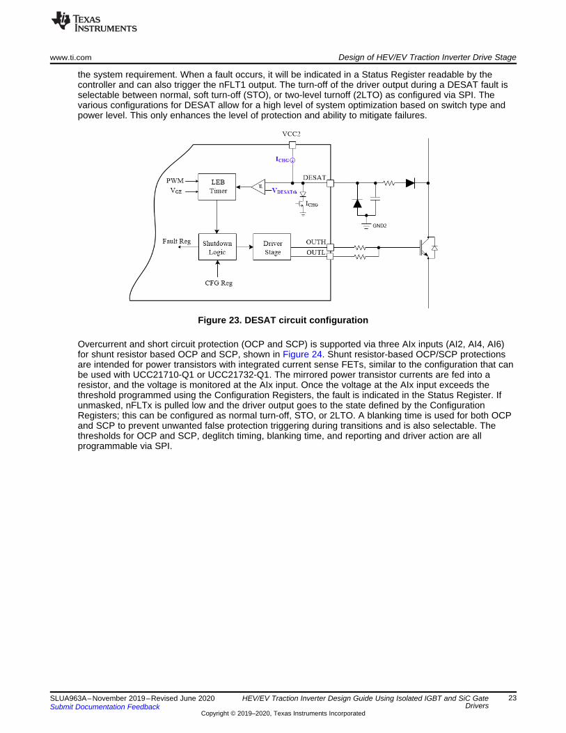
3.10.2 Programmable Desaturation (DESAT) Detection and Over-Current (OC)DESAT protection prevents the power transistor from damage in case of short circuit faults, which can bea result of incorrect control signals or a mechanical short. The DESAT input monitors the VCEsat(IGBT)/VDSon (MOSFET) through an external resistor and diode network, shown in Figure 23. Theconfiguration of the DESAT pin is the same as the UCC21750-Q1. However, SPI programming enablesthe thresholds, blanking time, charging current, and deglitch filters to be programmable in order to best fit
www.ti.com Design of HEV/EV Traction Inverter Drive Stage
23SLUA963A–November 2019–Revised June 2020Submit Documentation Feedback
Copyright © 2019–2020, Texas Instruments Incorporated
HEV/EV Traction Inverter Design Guide Using Isolated IGBT and SiC GateDrivers
the system requirement. When a fault occurs, it will be indicated in a Status Register readable by thecontroller and can also trigger the nFLT1 output. The turn-off of the driver output during a DESAT fault isselectable between normal, soft turn-off (STO), or two-level turnoff (2LTO) as configured via SPI. Thevarious configurations for DESAT allow for a high level of system optimization based on switch type andpower level. This only enhances the level of protection and ability to mitigate failures.
Figure 23. DESAT circuit configuration
Overcurrent and short circuit protection (OCP and SCP) is supported via three AIx inputs (AI2, AI4, AI6)for shunt resistor based OCP and SCP, shown in Figure 24. Shunt resistor-based OCP/SCP protectionsare intended for power transistors with integrated current sense FETs, similar to the configuration that canbe used with UCC21710-Q1 or UCC21732-Q1. The mirrored power transistor currents are fed into aresistor, and the voltage is monitored at the AIx input. Once the voltage at the AIx input exceeds thethreshold programmed using the Configuration Registers, the fault is indicated in the Status Register. Ifunmasked, nFLTx is pulled low and the driver output goes to the state defined by the ConfigurationRegisters; this can be configured as normal turn-off, STO, or 2LTO. A blanking time is used for both OCPand SCP to prevent unwanted false protection triggering during transitions and is also selectable. Thethresholds for OCP and SCP, deglitch timing, blanking time, and reporting and driver action are allprogrammable via SPI.

Design of HEV/EV Traction Inverter Drive Stage www.ti.com
24 SLUA963A–November 2019–Revised June 2020Submit Documentation Feedback
Copyright © 2019–2020, Texas Instruments Incorporated
HEV/EV Traction Inverter Design Guide Using Isolated IGBT and SiC GateDrivers
Figure 24. OC circuit configuration
3.10.3 Adjustable 2-Level or Soft Turn-OffAs mentioned in the previous sections, DESAT and OCP/SCP send back a fault indication and triggers thedriver to turn off the IGBT or SiC MOSFET. The driver initiates either 2-level turn-off or soft turn-off tosafely shut down the IGBT or MOSFET, preventing large voltage overshoot across the device as a resultof the high current transient.
The two-level turn-off (2LTOFF) function limits the transistor current during shutoff during certain faultconditions. When 2LTOFF is triggered, the gate of the power transistor is controlled to operate thetransistor in the linear region where the channel current is controlled by the voltage level on the gateterminal. The power transistor current is reduced by controlling the gate voltage to a intermediate voltage,or plateau voltage, (V2LOFF) for t2LOFF, and then ramping the gate down to turn the power transistor off.While 2LTOFF is active, OUTL sinks current to discharge the gate capacitor of the power switch to theplateau voltage. The plateau voltage level and duration are configurable. After holding the plateau voltagefor the programmed time, the gate is discharged fully using the soft turn-off current or pulled low as normalwith the OUTL driver. The soft turn off current can be enabled and level chosen in the ConfigurationRegisters.
The soft turn-off (STO) function is another method of protecting the power transistors from OV damagebecause of parasitic loop inductance induced voltage spikes on VCE. The STO slows down the turn-offprocess to limit the di/dt rate, and limiting the loop inductance-induced voltage spikes. During STO, theOUTL drive strength is reduced to the threshold programmed using SPI. The STO function is enabled forSC/OC and/or DESAT faults.
The inverter benefits not only to prevent the damage or destruction of the power switches, but alsoprevents high-voltages from being applied to the motor windings, which can also reduce the lifetime of themotor itself.
www.ti.com Design of HEV/EV Traction Inverter Drive Stage
25SLUA963A–November 2019–Revised June 2020Submit Documentation Feedback
Copyright © 2019–2020, Texas Instruments Incorporated
HEV/EV Traction Inverter Design Guide Using Isolated IGBT and SiC GateDrivers
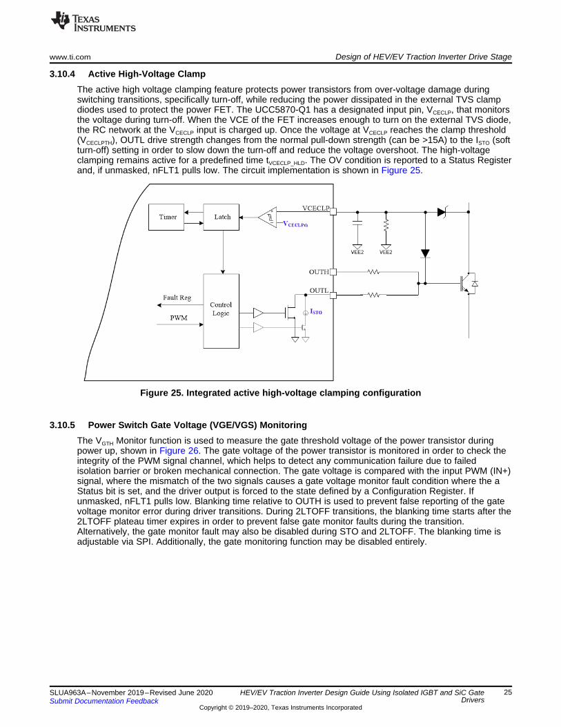
3.10.4 Active High-Voltage ClampThe active high voltage clamping feature protects power transistors from over-voltage damage duringswitching transitions, specifically turn-off, while reducing the power dissipated in the external TVS clampdiodes used to protect the power FET. The UCC5870-Q1 has a designated input pin, VCECLP, that monitorsthe voltage during turn-off. When the VCE of the FET increases enough to turn on the external TVS diode,the RC network at the VCECLP input is charged up. Once the voltage at VCECLP reaches the clamp threshold(VCECLPTH), OUTL drive strength changes from the normal pull-down strength (can be >15A) to the ISTO (softturn-off) setting in order to slow down the turn-off and reduce the voltage overshoot. The high-voltageclamping remains active for a predefined time tVCECLP_HLD. The OV condition is reported to a Status Registerand, if unmasked, nFLT1 pulls low. The circuit implementation is shown in Figure 25.
Figure 25. Integrated active high-voltage clamping configuration
3.10.5 Power Switch Gate Voltage (VGE/VGS) MonitoringThe VGTH Monitor function is used to measure the gate threshold voltage of the power transistor duringpower up, shown in Figure 26. The gate voltage of the power transistor is monitored in order to check theintegrity of the PWM signal channel, which helps to detect any communication failure due to failedisolation barrier or broken mechanical connection. The gate voltage is compared with the input PWM (IN+)signal, where the mismatch of the two signals causes a gate voltage monitor fault condition where the aStatus bit is set, and the driver output is forced to the state defined by a Configuration Register. Ifunmasked, nFLT1 pulls low. Blanking time relative to OUTH is used to prevent false reporting of the gatevoltage monitor error during driver transitions. During 2LTOFF transitions, the blanking time starts after the2LTOFF plateau timer expires in order to prevent false gate monitor faults during the transition.Alternatively, the gate monitor fault may also be disabled during STO and 2LTOFF. The blanking time isadjustable via SPI. Additionally, the gate monitoring function may be disabled entirely.

Design of HEV/EV Traction Inverter Drive Stage www.ti.com
26 SLUA963A–November 2019–Revised June 2020Submit Documentation Feedback
Copyright © 2019–2020, Texas Instruments Incorporated
HEV/EV Traction Inverter Design Guide Using Isolated IGBT and SiC GateDrivers
Figure 26. Gate voltage monitor
3.10.6 Gate Threshold Voltage MonitorAs a diagnostic feature, the gate threshold voltage monitor feeds back the measured threshold voltage tothe MCU to judge the health of the power transistor, as described in Figure 27 and Figure 28. This ishelpful in determining system lifetime and the potential for a failure later in time. The gate thresholdvoltage monitor measures the actual threshold voltage of the SiC MOSFET or IGBT. When enabled, theswitch between DESAT and OUTH is turned on and a constant current source charges the gatecapacitance of the power transistor, causing the gate voltage to ramp up gradually. Once the transistorchannel starts to conduct, the gate voltage is naturally held at the threshold voltage level as the powertransistor is in a diode configuration. After the blanking time, tdVGTHM, the integrated ADC samples the gatevoltage, and reports the measurement to the ADC Data Register.
Figure 27. Gate voltage threshold monitoring while gate capacitor charges

www.ti.com Design of HEV/EV Traction Inverter Drive Stage
27SLUA963A–November 2019–Revised June 2020Submit Documentation Feedback
Copyright © 2019–2020, Texas Instruments Incorporated
HEV/EV Traction Inverter Design Guide Using Isolated IGBT and SiC GateDrivers
Figure 28. Gate voltage threshold monitoring while power transistor is in diode configuration
3.10.7 Power Switch Anti-Shoot-ThroughThe shoot through protection (STP) function provides an additional layer of protection from shoot throughconditions due to incorrect PWM commands from MCU. The output of the driver uses IN+ and thecomplementary PWM signal provided to the IN- input to set the output state of the driver, as shown inFigure 29. Both the IN+ and IN- inputs are deglitched, which is programmable. Additionally, the output ofthe driver only goes high once the deglitched IN+ is high and for a programmable dead time after thedeglitched IN- is low. If IN+ and IN- are both high at the same time, a shoot-through condition is detected,and is reported to a Status Register and, if unmasked, the nFLT1 output pulls low. The output of the driveris forced to the state defined by a Configuration setting. The STP function is disabled by setting the deadtime to be 0 and connecting the IN- input low so the output simply follows IN+.
Figure 29. Shoot-through protection
3.10.8 Active Short Circuit (ASC)The active short circuit (ASC) function allows the system to force the state of the power transistorregardless of the PWM input. The ASC interface is located on both the primary and secondary sides,depending on the architecture of the safety controller. For cases where the main MCU is not available dueto fault or otherwise, a secondary control circuit drives the ASC_EN input high to force the output of theUCC5870-Q1 to the state defined by the ASC input, denoted as the HV Controller in Figure 30.

VDD
Error
nRST
WDWDSPI
PMIC MCU
VBAT
INP
Control
Logic
Charge
Pump
RGON
CBST
DBST
OUTH
OUTL
GND2
VBST
VEE2
RGOFF
AI5
AI6
ASC
ASC_EN
ASC_IN
ASC_IN Isola
tio
n B
arr
ier
HV Controller
ASC_ENASC_EN
Design of HEV/EV Traction Inverter Drive Stage www.ti.com
28 SLUA963A–November 2019–Revised June 2020Submit Documentation Feedback
Copyright © 2019–2020, Texas Instruments Incorporated
HEV/EV Traction Inverter Design Guide Using Isolated IGBT and SiC GateDrivers
From system point of view, the implementation of ASC function is to control the inverter output to be azero vector. The zero vector can be generated through two approaches: Main MCU or secondary controlcircuit. The ASC function is usually triggered when there is a system fault. If the fault is not a MCU fault,the MCU can implement diagnosis through the SPI interface and generate the appropriate zero vectorbased on fault type. If the fault happens in the MCU, then the secondary control circuit pulls the ASC_ENpin to be HIGH and suitable state on the ASC pin. With the ASC_EN pin pulled high, the driver outputfollows the state on the ASC pin. For the primary side, two dedicated inputs are available for the ASCcontrol. The ASC control is also available on the secondary side using the AI5 and AI6 inputs. The driveris configured with the secondary ASC function using SPI. In this configuration, AI5 works as ASC_EN andAI6 is the ASC input. The primary and secondary ASC interfaces are shown in Figure 30.
Figure 30. ASC primary and secondary side interfaces
3.10.9 Integrated Internal or External Miller ClampThe Active Miller clamp (CLAMP) is used to prevent the power transistor from false turn-on due to Millercapacitance-induced current. The active Miller clamp adds a low impedance path between powertransistor gate terminal and VEE2 to pull the gate of the external FET hard to VEE2, bypassing anyexternal gate resistors. The Miller clamp engages when the OUTH pin falls below VCLPTH, which is thethreshold voltage that can be selected using SPI programming. The integrated internal Miller Clamp isshown in Figure 31. The CLAMP pin can also be configured to drive an external Miller Clamp FET if morepull-down strength is required, as shown in Figure 32. The external Miller Clamp FET also provides theability to optimize placement of the clamp such that it is very close to the gate of the power transistor.Both options can be easily tested by configuring the output using SPI and making minor changes to thelayout.
Figure 31. Integrated Internal Miller Clamp

10bit ADCMUX
VCC2
VCC2
CLAMP
ITOx
CHSEL
OUTH
OUTL
General purpose
General purpose
General purpose
DC Link Voltage
OC/SC current
Temperature
GND2
AI1
AI2
AI3
AI4
AI5
AI6
www.ti.com Design of HEV/EV Traction Inverter Drive Stage
29SLUA963A–November 2019–Revised June 2020Submit Documentation Feedback
Copyright © 2019–2020, Texas Instruments Incorporated
HEV/EV Traction Inverter Design Guide Using Isolated IGBT and SiC GateDrivers
Figure 32. Integrated Driver for External Miller Clamp
3.10.10 Isolated Analog-to-Digital ConverterThe isolated ADC can be used for a variety of purposes, as shown in Figure 33. Already mentioned arethe OCP/SCP protection and ASC configurations. In addition to this, the temperature of the powermodules can also be monitored by configuring specified AIx channels to bias external temperaturesensors. This is described in the following section. Other potential uses for the ADC to enable a high levelof system failure mode coverage would be DC link voltage monitoring through a resistor divider, and otherDC levels. The 10-bit ADC has a full scale voltage range of 0V to 3.6V and has a total error of 1.5%. Thereference voltage can be chosen as external or internal depending on accuracy requirements. The internalvoltage reference has a 5% tolerance. The ADC conversions are aligned with the INP signal to ensureminimal noise coupling from the switching transients. All data is stored in the ADC data registered whichcan be read via SPI. There are three sampling modes available to ensure the least amount of switchingnoise in the measurement: Center aligned, Edge, and Hybrid modes.
Figure 33. ADC implementation example
3.10.10.1 Temperature Monitoring of Power TransistorUCC5870-Q1 designates three AIx inputs (AI1, AI3, AI5) to support thermal diode sensing for up to threepower transistors sharing the same ground reference. An example with a single thermal diodemeasurement is shown in Figure 34. The temperature protection is intended for power transistors withintegrated temperature sensing diodes in order to monitor the junction temperature, which can be anindication for the controller to discontinue to operate the inverter or as a mode of failure. The AIx input

Design of HEV/EV Traction Inverter Drive Stage www.ti.com
30 SLUA963A–November 2019–Revised June 2020Submit Documentation Feedback
Copyright © 2019–2020, Texas Instruments Incorporated
HEV/EV Traction Inverter Design Guide Using Isolated IGBT and SiC GateDrivers
provides a current that biases the integrated diode, and the voltage is monitored at the AIx input. The biascurrent can be enabled via SPI on one or all of the available AI pins. The temperature measurement is fedback into the ADC Data register, and a fault can also be configured for thermal shutdown (TSD) or thermalwarning (TWN). The fault must exist for the deglitch time programmed before the fault is registered. TheAIx pins can be enabled/disabled for temperature monitoring.
Figure 34. Power switch temperature monitoring
3.10.11 Short-Circuit ClampingIntegrated diodes protect the OUTH and CLAMP outputs during short circuit conditions. The short circuitclamping function clamps the voltages at the driver output (OUTH) and active Miller clamp (CLAMP)outputs to be slightly higher than VCC2 during power switch short circuit conditions. The clamped gatevoltage limits the short circuit current and prevents the IGBT/MOSFET gate from overvoltage breakdownor degradation.
3.10.12 Active and Passive PulldownWhile VCC2 is unpowered, the gate of the external power switch his held off with a passive and activepulldown circuit. The passive pulldown continuous bleeds charge off the gate of the power transistorthrough a resistor. If the OUTL suddenly rises due to ramping VCC2 during power up, the active pull-downfunction pulls the IGBT/MOSFET gate to the low state.
3.10.13 Thermal Shutdown and Temperature Warning of Driver ICThe driver IC also has integrated thermal monitoring to prevent failure during overheating conditions. Boththe primary and secondary sides of the driver utilize thermal warning and shutdown comparators to helpmitigate damage due to high temperatures. When a thermal warning is detected on the primary side, theStatus is set and, if unmasked, a fault is reported. If an over-temperature event is detected on the primaryside, the device transitions to the RESET state where the driver output is held low. Once the device cools,the UCC5870-Q1 must be reconfigured. If a thermal warning is detected on the secondary side, the Statusis set and, if unmasked, the fault is reported. When a thermal shutdown is detected on the secondary side,the driver is disabled, the Status is set and, if unmasked, the fault is reported. Once the driver cools andthe fault clears, the UCC5870-Q1 must be reconfigured.

www.ti.com Design of HEV/EV Traction Inverter Drive Stage
31SLUA963A–November 2019–Revised June 2020Submit Documentation Feedback
Copyright © 2019–2020, Texas Instruments Incorporated
HEV/EV Traction Inverter Design Guide Using Isolated IGBT and SiC GateDrivers
3.10.14 Clock Monitor and CRCThe UCC5870-Q1 integrates clock monitor functions to identify clock faults during operation. The Clockmonitor detects internal oscillator failures such as: oscillator clock stuck high or stuck low and clockfrequency out of range. The clock monitor is enabled during a power-up event after the power-on reset isreleased. The clocks on both the primary side and secondary side are monitored. In the event of a clockfault on the primary side, Status is set and, if unmasked, the fault output pulls low. The primary side clockmonitor has no effect on the gate driver output state. In the event of a clock fault on the secondary side,the Status is set, and the driver output is forced to the state determined by the user-set Configuration,and, if unmasked, the fault output pulls low.
The clock monitor circuit also integrates a diagnostic that checks the integrity of the monitoring circuit. Thediagnostic is run automatically during the start up process. Additionally, a simulated clock monitor fault canbe generated by writing to the respective Control bits for the primary or secondary sides. When enabled,the diagnostics emulates clock failure that causes a clock monitor fault. During this self-test, the actualoscillator frequency is not changed.
Additionally, UCC5870-Q1 uses a cyclic redundancy check (CRC) to ensure data integrity for theconfiguration of the device while the driver output is active, the SPI communications (both transmitted andreceived), and the internal non-volatile memory that stores the trim information ensuring the performanceof the device.
3.10.15 SPI and Register Data ProtectionSPI input and output data integrity is monitored as well as register data content. This is to ensure propercommunications and storage of data for setting driver parameters and functions.
When the UCC5870-Q1 transitions to the ACTIVE state, the contents of configuration and control registersare protected by CRC engine. The configuration CRC is enabled using the proper Configuration bit. Thevarious registers protected by the CRC are outlined in the datasheet. The CRC fault detection isperformed every tCRCCFG (typically 1 ms). If the calculated CRC checksum for the configuration registersdoes not match the CRC checksum calculated upon entering the Active state, Status bits are set and, ifunmasked, the nFLT1 output goes low. Additionally, for the secondary side CRC failure, the driver outputis forced to the state pre-defined in a Configuration register. Diagnostics for the CRC check are alsoavailable. A Control Register can be commanded to induce a CRC error on the primary or secondary side.
The CRC that checks for SPI transfer are continuously updated as SPI traffic is received/sent. The CRC isupdated with every 16-bits that are received. In this set of commands, the configuration is updated andcompared on that command.
The SDI CRC checksum data is continuously calculated as SPI data frames are received. Once the MCUwrites to the to CRC Data Transmission (TX) bits, this triggers a comparison of the data in the CRC TXbits with the internally calculated CRC. Once the comparison is complete, the CRC calculation logic isreset. When there is a mismatch between CRC TX data and CRC calculated internally, the Status bit isset and, if unmasked, the nFLT1 output pulls low and the output is set based on the pre-configuredregister setting.
The SDO CRC checksum is continuously calculated as data is clocked out of SDO. The resulting CRC isstored in the CRC Receive (RX) Data bits. The bits are updated whenever chip select, nCS, transitionsfrom low to high. The CRC calculation logic is reset when the CRC RX bits are read.
After each power up, the UCC5870-Q1 performs a TRIM CRC check on the internal non-volatile memoryon both the primary and secondary sides. If the calculated CRC checksum does not match the CRCchecksum stored in the internal TRIM memory, Status bits are set and, if unmasked, the nFLT1 outputgoes low. Additionally for the secondary side CRC failure, the driver output is forced to the pre-definedstate.
Isolated
Supply
Gate
Driver 1
Gate
Driver 2
Gate
Driver 5
Gate
Driver 3
Gate
Driver 4
Gate
Driver 6
Isolated
Supply
Isolated
Supply
Isolated
Supply
Isolated
Supply
Gate
Driver 1
Gate
Driver 2
Gate
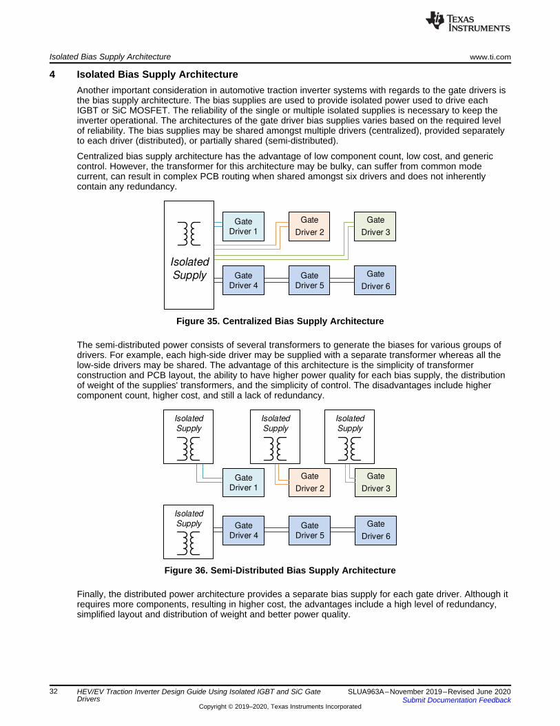
Driver 5
Gate
Driver 3
Gate
Driver 4
Gate
Driver 6
Isolated Bias Supply Architecture www.ti.com
32 SLUA963A–November 2019–Revised June 2020Submit Documentation Feedback
Copyright © 2019–2020, Texas Instruments Incorporated
HEV/EV Traction Inverter Design Guide Using Isolated IGBT and SiC GateDrivers
4 Isolated Bias Supply ArchitectureAnother important consideration in automotive traction inverter systems with regards to the gate drivers isthe bias supply architecture. The bias supplies are used to provide isolated power used to drive eachIGBT or SiC MOSFET. The reliability of the single or multiple isolated supplies is necessary to keep theinverter operational. The architectures of the gate driver bias supplies varies based on the required levelof reliability. The bias supplies may be shared amongst multiple drivers (centralized), provided separatelyto each driver (distributed), or partially shared (semi-distributed).
Centralized bias supply architecture has the advantage of low component count, low cost, and genericcontrol. However, the transformer for this architecture may be bulky, can suffer from common modecurrent, can result in complex PCB routing when shared amongst six drivers and does not inherentlycontain any redundancy.
Figure 35. Centralized Bias Supply Architecture
The semi-distributed power consists of several transformers to generate the biases for various groups ofdrivers. For example, each high-side driver may be supplied with a separate transformer whereas all thelow-side drivers may be shared. The advantage of this architecture is the simplicity of transformerconstruction and PCB layout, the ability to have higher power quality for each bias supply, the distributionof weight of the supplies' transformers, and the simplicity of control. The disadvantages include highercomponent count, higher cost, and still a lack of redundancy.
Figure 36. Semi-Distributed Bias Supply Architecture
Finally, the distributed power architecture provides a separate bias supply for each gate driver. Although itrequires more components, resulting in higher cost, the advantages include a high level of redundancy,simplified layout and distribution of weight and better power quality.

Isolated
Supply
Isolated
Supply
Isolated
Supply
Isolated
Supply
Isolated
Supply
Isolated
Supply
Gate
Driver 1
Gate
Driver 2
Gate
Driver 5
Gate
Driver 3
Gate
Driver 4
Gate
Driver 6
www.ti.com Isolated Bias Supply Architecture
33SLUA963A–November 2019–Revised June 2020Submit Documentation Feedback
Copyright © 2019–2020, Texas Instruments Incorporated
HEV/EV Traction Inverter Design Guide Using Isolated IGBT and SiC GateDrivers
Figure 37. Distributed Bias Supply Architecture
For more information on bias supplies, please see TI's portfolio of high-voltage controllers and thisreference design on bias supplies for HEV/EV traction inverters.

Summary www.ti.com
34 SLUA963A–November 2019–Revised June 2020Submit Documentation Feedback
Copyright © 2019–2020, Texas Instruments Incorporated
Revision History
5 SummaryThe complexity of electronics in electrified vehicles is ever-increasing with enhanced performance andsafety regulations. The traction inverter contains some of the most critical components of the electricvehicle which have a direct impact on the drive of the motor. Integrated protection and monitoring featuresof UCC217xx-Q1 and UCC5870-Q1 drivers are shown to enable simplification of the system, as well asenhanced performance.
For more information, please see the product folders of UCC21732-Q1,UCC21750-Q1, UCC21710-Q1and UCC5870-Q1 containing design help and technical documentation and visit the Power ManagementE2E Forum to get answers to your questions.
6 References1. HEV/EV traction inverter power stage with 3 types of IGBT/SiC bias-supply solutions reference design2. UCC217xx Family Driving and Protecting SiC and IGBT Power Modules and Transistor3. Understanding the Short Circuit Protection for Silicon Carbide MOSFETs4. SiC/IGBT Isolated Gate Driver Reference Design With Thermal Diode and Sensing FET5. J. Drobnik and P. Jain, "Electric and hybrid vehicle power electronics efficiency, testing and reliability,"
2013 World Electric Vehicle Symposium and Exhibition (EVS27), Barcelona, 2013, pp. 1-12.6. Haizhong Ye, Y. Yang and A. Emadi, "Traction inverters in hybrid electric vehicles," 2012 IEEE
Transportation Electrification Conference and Expo (ITEC), Dearborn, MI, 2012, pp. 1-6.7. S. Jain and L. Kumar, "Fundamentals of Power Electronics Controlled Electric Propulsion," in Power
Electronics Handbook, M. H. Rashid, Ed. United Kingdom: Butterworth-Heinemann, 2018, pp. 1023-1065.
Revision HistoryNOTE: Page numbers for previous revisions may differ from page numbers in the current version.
Changes from Original (November 2019) to A Revision ................................................................................................ Page
• Added additional detail throughout. .................................................................................................... 1

35SLUA963A–November 2019–Revised June 2020Submit Documentation Feedback
Copyright © 2019–2020, Texas Instruments Incorporated

IMPORTANT NOTICE AND DISCLAIMER
TI PROVIDES TECHNICAL AND RELIABILITY DATA (INCLUDING DATASHEETS), DESIGN RESOURCES (INCLUDING REFERENCE DESIGNS), APPLICATION OR OTHER DESIGN ADVICE, WEB TOOLS, SAFETY INFORMATION, AND OTHER RESOURCES “AS IS” AND WITH ALL FAULTS, AND DISCLAIMS ALL WARRANTIES, EXPRESS AND IMPLIED, INCLUDING WITHOUT LIMITATION ANY IMPLIED WARRANTIES OF MERCHANTABILITY, FITNESS FOR A PARTICULAR PURPOSE OR NON-INFRINGEMENT OF THIRD PARTY INTELLECTUAL PROPERTY RIGHTS.These resources are intended for skilled developers designing with TI products. You are solely responsible for (1) selecting the appropriate TI products for your application, (2) designing, validating and testing your application, and (3) ensuring your application meets applicable standards, and any other safety, security, or other requirements. These resources are subject to change without notice. TI grants you permission to use these resources only for development of an application that uses the TI products described in the resource. Other reproduction and display of these resources is prohibited. No license is granted to any other TI intellectual property right or to any third party intellectual property right. TI disclaims responsibility for, and you will fully indemnify TI and its representatives against, any claims, damages, costs, losses, and liabilities arising out of your use of these resources.TI’s products are provided subject to TI’s Terms of Sale (www.ti.com/legal/termsofsale.html) or other applicable terms available either on ti.com or provided in conjunction with such TI products. TI’s provision of these resources does not expand or otherwise alter TI’s applicable warranties or warranty disclaimers for TI products.
Mailing Address: Texas Instruments, Post Office Box 655303, Dallas, Texas 75265Copyright © 2020, Texas Instruments Incorporated