software-defined radio handbook · 2016-06-15 · software-defined radio handbook 0fsig mixer...
TRANSCRIPT

PPPPPentek, Inc.entek, Inc.entek, Inc.entek, Inc.entek, Inc. • One Park Way, Upper Saddle River, NJ 07458 • Tel: (201) 818-5900 • Fax: (201) 818-5904 • Email: [email protected] • http://www.pentek.com
11111
SoSoSoSoSoffffftttttware-Defined Rware-Defined Rware-Defined Rware-Defined Rware-Defined Radio Handbookadio Handbookadio Handbookadio Handbookadio Handbook11th Edition
PPPPPentek, Inc.entek, Inc.entek, Inc.entek, Inc.entek, Inc.One Park Way, Upper Saddle River, New Jersey 07458
Tel: (201) 818-5900 • Fax: (201) 818-5904Email: [email protected] • http://www.pentek.com
Copyright © 1998, 2001, 2003, 2006, 2008, 2009, 2010, 2011, 2012, 2013, 2014, 2015 Pentek, Inc.Last updated: November 2015
All rights reserved.Contents of this publication may not be reproduced in any form without written permission.
Specifications are subject to change without notice.Pentek, GateFlow, ReadyFlow, SystemFlow, Cobalt, Onyx, Talon, Bandit, Flexor, GateXpress, SPARK, and QuickPac are trademarks or registered trademarks of Pentek, Inc.
Other trademarks are properties of their respective owners.
SamplingSamplingSamplingSamplingSampling
PPPPPrinciples of SDRrinciples of SDRrinciples of SDRrinciples of SDRrinciples of SDR
TTTTTechnologyechnologyechnologyechnologyechnology
PPPPProductsroductsroductsroductsroducts
ApplicationsApplicationsApplicationsApplicationsApplications
by
RRRRRodger Hodger Hodger Hodger Hodger H. Hosking. Hosking. Hosking. Hosking. HoskingVice-President & Cofounder of Pentek, Inc.
®

PPPPPentek, Inc.entek, Inc.entek, Inc.entek, Inc.entek, Inc. • One Park Way, Upper Saddle River, NJ 07458 • Tel: (201) 818-5900 • Fax: (201) 818-5904 • Email: [email protected] • http://www.pentek.com
22222
Software-Defined Radio Handbook
Preface
SDR (Software-Defined Radio) has revolutionized electronic systems for avariety of applications including communications, data acquisition and signal processing.
This handbook shows how DDCs (Digital Downconverters) and DUCs (Digital Upconverters),the fundamental building blocks of SDR, can replace legacy analog receiver and transmitter designs while
offering significant benefits in performance, density and cost.
In order to fully appreciate the benefits of SDR, conventional analog receiver and transmittersystems will be compared to their digital counterparts, highlighting similarities and differences.
The inner workings of the SDR will be explored with an in-depth description of the internalstructure and the devices used. Finally, some actual board- and system-level implementations and available
off-the-shelf SDR products and applications based on such products will be presented.
For more information on complementary subjects, the reader is referred to these Pentek Handbooks:Putting FPGAs to Work in Software Radio Systems
Critical Techniques for High-Speed A/D Converters in Real-Time Systems
High-Speed Switched Serial Fabrics Improve System Design
High-Speed, Real-Time Recording Systems

PPPPPentek, Inc.entek, Inc.entek, Inc.entek, Inc.entek, Inc. • One Park Way, Upper Saddle River, NJ 07458 • Tel: (201) 818-5900 • Fax: (201) 818-5904 • Email: [email protected] • http://www.pentek.com
33333
Software-Defined Radio Handbook
Before we look at SDR and its various implementa-tions in embedded systems, we’ll review a theoremfundamental to sampled data systems such as thoseencountered in Software-Defined Radios.
Nyquist’s Theorem:
“Any signal can be represented by discretesamples if the sampling frequency is at least twice
the bandwidth of the signal.”
Notice that we highlighted the word bandwidthrather than frequency. In what follows, we’ll attempt toshow the implications of this theorem and the correctinterpretation of sampling frequency, also known assampling rate.
SamplingSamplingSamplingSamplingSampling
A Simple TA Simple TA Simple TA Simple TA Simple Technique to Visualize Samplingechnique to Visualize Samplingechnique to Visualize Samplingechnique to Visualize Samplingechnique to Visualize Sampling
To visualize what happens in sampling, imagine thatyou are using transparent “fan-fold” computer paper.Use the horizontal edge of the paper as the frequencyaxis and scale it so that the paper folds line up withinteger multiples of one-half of the sampling frequency ƒs.Each sheet of paper now represent what we will call a“Nyquist Zone”, as shown in Figure 1.
Figure 1
Nyquist’s Theorem and SamplingNyquist’s Theorem and SamplingNyquist’s Theorem and SamplingNyquist’s Theorem and SamplingNyquist’s Theorem and Sampling
fs/2 fs 3fs/2 2fs 5fs/2 3fs 7fs/20
Zone 1 Zone 2 Zone 3 Zone 4 Zone 5 Zone 6 Zone 7
Frequency
PPPPPentek, Inc.entek, Inc.entek, Inc.entek, Inc.entek, Inc. • One Park Way, Upper Saddle River, NJ 07458 • Tel: (201) 818-5900 • Fax: (201) 818-5904 • Email: [email protected] • http://www.pentek.com
44444
Software-Defined Radio Handbook
SamplingSamplingSamplingSamplingSampling
Figure 3
Baseband SamplingBaseband SamplingBaseband SamplingBaseband SamplingBaseband Sampling
Figure 4
A baseband signal has frequency components thatstart at ƒ = 0 and extend up to some maximum frequency.
To prevent data destruction when sampling a basebandsignal, make sure that all the signal energy falls ONLY inthe 1st Nyquist band, as shown in Figure 4.
There are two ways to do this:1. Insert a lowpass filter to eliminate all signals
above ƒs/2, or2. Increase the sampling frequency so all signals
present fall below ƒs/2.
Note that ƒs/2 is also known as the “folding frequency”.
Sampling Bandpass SignalsSampling Bandpass SignalsSampling Bandpass SignalsSampling Bandpass SignalsSampling Bandpass Signals
Figure 2
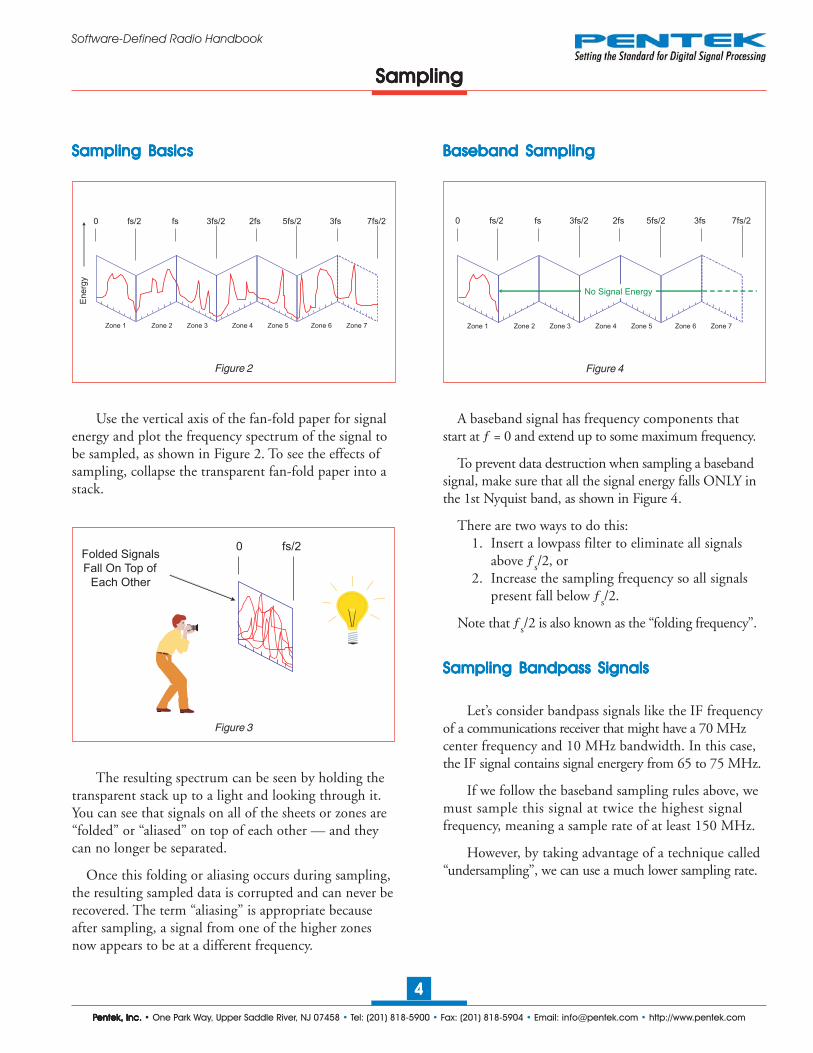
Use the vertical axis of the fan-fold paper for signalenergy and plot the frequency spectrum of the signal tobe sampled, as shown in Figure 2. To see the effects ofsampling, collapse the transparent fan-fold paper into astack.
Sampling BasicsSampling BasicsSampling BasicsSampling BasicsSampling Basics
The resulting spectrum can be seen by holding thetransparent stack up to a light and looking through it.You can see that signals on all of the sheets or zones are“folded” or “aliased” on top of each other — and theycan no longer be separated.
Once this folding or aliasing occurs during sampling,the resulting sampled data is corrupted and can never berecovered. The term “aliasing” is appropriate becauseafter sampling, a signal from one of the higher zonesnow appears to be at a different frequency.
Let’s consider bandpass signals like the IF frequencyof a communications receiver that might have a 70 MHzcenter frequency and 10 MHz bandwidth. In this case,the IF signal contains signal energery from 65 to 75 MHz.
If we follow the baseband sampling rules above, wemust sample this signal at twice the highest signalfrequency, meaning a sample rate of at least 150 MHz.
However, by taking advantage of a technique called“undersampling”, we can use a much lower sampling rate.
fs/2 fs 3fs/2 2fs 5fs/2 3fs 7fs/20
Zone 1 Zone 2 Zone 3 Zone 4 Zone 5 Zone 6 Zone 7
En
erg
y
fs/2 fs 3fs/2 2fs 5fs/2 3fs 7fs/20
Zone 1 Zone 2 Zone 3 Zone 4 Zone 5 Zone 6 Zone 7
No Signal Energy
fs/20Folded Signals
Fall On Top of
Each Other

PPPPPentek, Inc.entek, Inc.entek, Inc.entek, Inc.entek, Inc. • One Park Way, Upper Saddle River, NJ 07458 • Tel: (201) 818-5900 • Fax: (201) 818-5904 • Email: [email protected] • http://www.pentek.com
55555
Software-Defined Radio Handbook
fs/20
Folded signals
still fall on top of
each other - but
now there is
energy in
only one sheet !
UndersamplingUndersamplingUndersamplingUndersamplingUndersampling
Figure 5
SamplingSamplingSamplingSamplingSampling
Figure 6
fs/2 fs 3fs/2 2fs 5fs/2 3fs 7fs/20
Zone 1 Zone 2 Zone 3 Zone 4 Zone 5 Zone 6 Zone 7
No Signal EnergyNo Signal Energy
Undersampling allows us to use aliasing to ouradvantage, providing we follow the strict rules of theNyquist Theorem.
In our previous IF signal example, suppose we try asampling rate of 40 MHz.
Figure 5 shows a fan-fold paper plot with Fs = 40 MHz.You can see that zone 4 extends from 60 MHz to 80 MHz,nicely containing the entire IF signal band of 65 to 75 MHz.
Now when you collapse the fan fold sheets as shownin Figure 6, you can see that the IF signal is preservedafter sampling because we have no signal energy in anyother zone.
Also note that the odd zones fold with the lowerfrequency at the left (normal spectrum) and the evenzones fold with the lower frequency at the right (reversedspectrum).
In this case, the signals from zone 4 are frequency-reversed. This is usually very easy to accommodate inthe following stages of SDR systems.
SummarSummarSummarSummarSummaryyyyy
Baseband sampling requires the sample frequency tobe at least twice the signal bandwidth. This is the sameas saying that all of the signals fall within the firstNyquist zone.
In real life, a good rule of thumb is to use the 80%relationship:
Bandwidth = 0.8 * ƒs / 2 = 0.4 * ƒs
Undersampling allows a lower sample rate even thoughsignal frequencies are high, PROVIDED all of thesignal energy falls within one Nyquist zone.
To repeat the Nyquist theorem: The sampling frequencymust be at least twice the signal bandwidth — not thesignal frequency.
The major rule to follow for successful undersamplingis to make sure all of the energy falls entirely in oneNyquist zone.
There two ways to do this:1. Insert a bandpass filter to eliminate all signals
outside the one Nyquist zone.2. Increase the sampling frequency so all signals
fall entirely within one Nyquist zone.

PPPPPentek, Inc.entek, Inc.entek, Inc.entek, Inc.entek, Inc. • One Park Way, Upper Saddle River, NJ 07458 • Tel: (201) 818-5900 • Fax: (201) 818-5904 • Email: [email protected] • http://www.pentek.com
66666
Software-Defined Radio Handbook
Figure 7
The conventional heterodyne radio receiver shownin Figure 7, has been in use for nearly a century. Let’sreview the structure of the analog receiver so comparisonto a digital receiver becomes apparent.
First the RF signal from the antenna is amplified,typically with a tuned RF stage that amplifies a regionof the frequency band of interest.
This amplified RF signal is then fed into a mixerstage. The other input to the mixer comes from the localoscillator whose frequency is determined by the tuningcontrol of the radio.
The mixer translates the desired input signal to theIF (Intermediate Frequency) as shown in Figure 8.
The IF stage is a bandpass amplifier that only letsone signal or radio station through. Common centerfrequencies for IF stages are 455 kHz and 10.7 MHzfor commercial AM and FM broadcasts.
The demodulator recovers the original modulatingsignal from the IF output using one of several differentschemes.
For example, AM uses an envelope detector and FMuses a frequency discriminator. In a typical home radio,the demodulated output is fed to an audio power amplifierwhich drives a speaker.
Figure 8
Analog RAnalog RAnalog RAnalog RAnalog Radio Radio Radio Radio Radio Receiver Block Diagrameceiver Block Diagrameceiver Block Diagrameceiver Block Diagrameceiver Block Diagram Analog RAnalog RAnalog RAnalog RAnalog Radio Radio Radio Radio Radio Receiver Mixereceiver Mixereceiver Mixereceiver Mixereceiver Mixer
The mixer performs an analog multiplication of thetwo inputs and generates a difference frequency signal.
The frequency of the local oscillator is set so that thedifference between the local oscillator frequency and thedesired input signal (the radio station you want toreceive) equals the IF.
For example, if you wanted to receive an FMstation at 100.7 MHz and the IF is 10.7 MHz, you wouldtune the local oscillator to:
100.7 - 10.7 = 90 MHz
This is called “downconversion” or “translation”because a signal at a high frequency is shifted down to alower frequency by the mixer.
The IF stage acts as a narrowband filter which onlypasses a “slice” of the translated RF input. The band-width of the IF stage is equal to the bandwidth of thesignal (or the “radio station”) that you are trying toreceive.
For commercial FM, the bandwidth is about100 kHz and for AM it is about 5 kHz. This is consis-tent with channel spacings of 200 kHz and 10 kHz,respectively.
PPPPPrinciples of SDRrinciples of SDRrinciples of SDRrinciples of SDRrinciples of SDR
ANALOG
LOCAL
OSCILLATOR
IF AMP
(FILTER)
SPEAKER
ANTENNA
DEMODULATOR
(Detector)
ANALOG
MIXER
AUDIO
AMP
RF
AMP
0
RF INPUT SIGNAL
FROM ANTENNA
MIXER TRANSLATES
INPUT SIGNAL BAND
to IF FREQUENCY
ANALOG LOCAL
OSCILLATOR
FRFFIF
Signal

PPPPPentek, Inc.entek, Inc.entek, Inc.entek, Inc.entek, Inc. • One Park Way, Upper Saddle River, NJ 07458 • Tel: (201) 818-5900 • Fax: (201) 818-5904 • Email: [email protected] • http://www.pentek.com
77777
Software-Defined Radio Handbook
0 FSIG
MIXER TRANSLATES
INPUT SIGNAL
BAND to DC
DIGITAL LOCAL
OSCILLATOR
FLO = FSIG
CHANNEL
BANDWIDTH
IF BWSignal
DIGITAL
MIXER
DIGITAL
LOCAL
OSC
DSP
DDC
Digital Downconverter
RF
TUNER
Analog
IF Signal
Analog
RF SignalA/D
CONV
Digital IF
Samples LOWPASS
FILTER
Digital
Baseband
Samples
SDR RSDR RSDR RSDR RSDR Receiver Block Diagrameceiver Block Diagrameceiver Block Diagrameceiver Block Diagrameceiver Block Diagram
Figure 9
PPPPPrinciples of SDRrinciples of SDRrinciples of SDRrinciples of SDRrinciples of SDR
Figure 10
SDR RSDR RSDR RSDR RSDR Receiver Mixereceiver Mixereceiver Mixereceiver Mixereceiver MixerFigure 9 shows a block diagram of a softwaredefined radio receiver. The RF tuner converts analog RFsignals to analog IF frequencies, the same as the first threestages of the analog receiver.
The A/D converter that follows digitizes the IF signalthereby converting it into digital samples. These samplesare fed to the next stage which is the digital downconverter(DDC) shown within the dotted lines.
The digital downconverter is typically a singlemonolithic chip or FPGA IP, and it is a key part of theSDR system.
A conventional DDC has three major sections:
• A digital mixer
• A digital local oscillator
• An FIR lowpass filter
The digital mixer and local oscillator translate thedigital IF samples down to baseband. The FIR lowpassfilter limits the signal bandwidth and acts as a decimat-ing lowpass filter. The digital downconverter includes alot of hardware multipliers, adders and shift registermemories to get the job done.
The digital baseband samples are then fed to a blocklabeled DSP which performs tasks such as demodulation,decoding and other processing tasks.
Traditionally, these needs have been handled withdedicated application-specific ICs (ASICs), and program-mable DSPs.
At the output of the mixer, the high frequencywideband signals from the A/D input (shown in Figure10 above) have been translated down to DC as complex Iand Q components with a frequency shift equal to thelocal oscillator frequency.
This is similar to the analog receiver mixer exceptthere, the mixing was done down to an IF frequency.Here, the complex representation of the signal allows usto go right down to DC.
By tuning the local oscillator over its range, anyportion of the RF input signal can be mixed down to DC.
In effect, the wideband RF signal spectrum can be“slid” around 0 Hz, left and right, simply by tuning thelocal oscillator. Note that upper and lower sidebands arepreserved.

PPPPPentek, Inc.entek, Inc.entek, Inc.entek, Inc.entek, Inc. • One Park Way, Upper Saddle River, NJ 07458 • Tel: (201) 818-5900 • Fax: (201) 818-5904 • Email: [email protected] • http://www.pentek.com
88888
Software-Defined Radio Handbook
DIGITAL
MIXER
DIGITAL
LOCAL
OSC
A/D
CONV
Digital IF
SamplesLOWPASS
FILTER
Digital
Baseband
Samples
Translation Filtering
Tuning Freq Decimation
DDC Signal PDDC Signal PDDC Signal PDDC Signal PDDC Signal Processingrocessingrocessingrocessingrocessing
Figure 12
PPPPPrinciples of SDRrinciples of SDRrinciples of SDRrinciples of SDRrinciples of SDR
Figure 11A Local Oscillator Frequency Switching
DDC LDDC LDDC LDDC LDDC Local Oscillator and Decimationocal Oscillator and Decimationocal Oscillator and Decimationocal Oscillator and Decimationocal Oscillator and Decimation
F1 F2 F3
90O
A/D Sample Rate(before decimation)
Sample Rate: Fs
Decimated
Filter OutputSample Rate: Fs/N
Figure 11B FIR Filter Decimation
Because the local oscillator uses a digital phaseaccumulator, it has some very nice features. It switchesbetween frequencies with phase continuity, so you cangenerate FSK signals or sweeps very precisely with notransients as shown in Figure 11A.
The frequency accuracy and stability are determinedentirely by the A/D clock so it’s inherently synchronousto the sampling frequency. There is no aging, drift orcalibration since it’s implemented entirely with digital logic.
Since the output of the FIR filter is band-limited, theNyquist theorem allows us to lower the sample rate. Ifwe are keeping only one out of every N samples, as shownin Figure 11B above, we have dropped the sampling rateby a factor of N.
This process is called decimation and it means keepingone out of every N signal samples. If the decimatedoutput sample rate is kept higher than twice the outputbandwidth, no information is lost.
The clear benefit is that decimated signals can beprocessed easier, can be transmitted at a lower rate, orstored in less memory. As a result, decimation candramatically reduce system costs!
As shown in Figure 12, the DDC performs twosignal processing operations:
1. Frequency translation with the tuning controlledby the local oscillator.
2. Lowpass filtering with the bandwidth controlledby the decimation setting.
We will next turn our attention to the Software-Defined Radio Transmitter.

PPPPPentek, Inc.entek, Inc.entek, Inc.entek, Inc.entek, Inc. • One Park Way, Upper Saddle River, NJ 07458 • Tel: (201) 818-5900 • Fax: (201) 818-5904 • Email: [email protected] • http://www.pentek.com
99999
Software-Defined Radio Handbook
DUC Signal PDUC Signal PDUC Signal PDUC Signal PDUC Signal Processingrocessingrocessingrocessingrocessing
Figure 14
PPPPPrinciples of SDRrinciples of SDRrinciples of SDRrinciples of SDRrinciples of SDR
SDR TSDR TSDR TSDR TSDR Transmitter Block Diagramransmitter Block Diagramransmitter Block Diagramransmitter Block Diagramransmitter Block Diagram
Figure 13
The input to the transmit side of an SDR system isa digital baseband signal, typically generated by a DSPstage as shown in Figure 13 above.
The digital hardware block in the dotted lines is aDUC (digital upconverter) that translates the basebandsignal to the IF frequency.
The D/A converter that follows converts the digitalIF samples into the analog IF signal.
Next, the RF upconverter converts the analog IFsignal to RF frequencies.
Finally, the power amplifier boosts signal energy tothe antenna.
Inside the DUC shown in Figure 14, the digitalmixer and local oscillator at the right translate basebandsamples up to the IF frequency. The IF translationfrequency is determined by the local oscillator.
The mixer generates one output sample for each ofits two input samples. And, the sample frequency atthe mixer output must be equal to the D/A samplefrequency ƒs.
Therefore, the local oscillator sample rate and thebaseband sample rate must be equal to the D/A samplefrequency ƒs.
The local oscillator already operates at a sample rateof ƒs, but the input baseband sample frequency at theleft is usually much lower. This problem is solved withthe Interpolation Filter.
Digital
Baseband
Samples
Fs/N
DIGITAL
MIXER
DIGITAL
LOCAL
OSC
DUC
Digital Up
Converter
INTERPOLATION
FILTER
Digital IF
Samples
Fs
Digital
Baseband
Samples
Fs
DUC
Digital Up
Converter
Analog
IF
SignalD/A
CONV
Analog
RF
SignalRF
Upconverter
Power
AmplifierDSP
Digital
Baseband
Samples
Fs/N
DIGITAL
MIXER
DIGITAL
LOCAL
OSC
INTERPOLATION
FILTER
Digital IF
Samples
Fs
Digital
Baseband
Samples
Fs

PPPPPentek, Inc.entek, Inc.entek, Inc.entek, Inc.entek, Inc. • One Park Way, Upper Saddle River, NJ 07458 • Tel: (201) 818-5900 • Fax: (201) 818-5904 • Email: [email protected] • http://www.pentek.com
1010101010
Software-Defined Radio Handbook
Interpolation FInterpolation FInterpolation FInterpolation FInterpolation Filter: Time domainilter: Time domainilter: Time domainilter: Time domainilter: Time domain
Figure 15 Figure 16
Interpolation FInterpolation FInterpolation FInterpolation FInterpolation Filter: Filter: Filter: Filter: Filter: Frequency Domainrequency Domainrequency Domainrequency Domainrequency Domain
PPPPPrinciples of SDRrinciples of SDRrinciples of SDRrinciples of SDRrinciples of SDR
INTERPOLATING
LOW PASS
FIR FILTER
Fs/N
I
Q
INTERPOLATION
FACTOR = N
BASEBAND
INPUT
Interpolating
Filter OutputSample Rate: Fs
Baseband InputSample Rate: Fs/N
Fs
INTER-
POLATED
OUTPUT
I
Q
0 IF Freq
LOCAL
OSCILLATOR
F = IF Freq
MIXER
INTERPOLATED
BASEBAND INPUT TRANSLATED OUTPUT
Digital
Baseband
Samples
Fs/N
DIGITAL
MIXER
DIGITAL
LOCAL
OSC
DUC
Digital Up
Converter
INTERPOLATION
FILTER
Digital IF
Samples
Fs
Digital
Baseband
Samples
Fs
The interpolation filter must boost the basebandinput sample frequency of ƒs / N up to the requiredmixer input and D/A output sample frequency of ƒs.
The interpolation filter increases the sample frequencyof the baseband input signal by a factor N, known asthe interpolation factor.
At the bottom of Figure 15, the effect of theinterpolation filter is shown in the time domain.
Notice the baseband signal frequency content iscompletely preserved by filling in additional samples inthe spaces between the original input samples.
The signal processing operation performed by theinterpolation filter is the inverse of the decimation filterwe discussed previously in the DDC section.
Figure 16 is a frequency domain view of the digitalupconversion process.
This is exactly the opposite of the frequency domainview of the DDC in Figure 10.
The local oscillator setting is set equal to therequired IF signal frequency, just as with the DDC.

PPPPPentek, Inc.entek, Inc.entek, Inc.entek, Inc.entek, Inc. • One Park Way, Upper Saddle River, NJ 07458 • Tel: (201) 818-5900 • Fax: (201) 818-5904 • Email: [email protected] • http://www.pentek.com
1111111111
Software-Defined Radio Handbook
DIGITAL
MIXER
DIGITAL
LOCAL
OSC
¸ N
A/D
CONVLOWPASS
FILTER
Translation Filtering
DSP
Fs Fb
Tuning
Freq uency
Bandwidth
Deci mation
DIGITAL
MIXER
DIGITAL
LOCAL
OSC
´ N
INTERPOLATE
FILTER
TranslationFiltering
D/A
CONVDSP
Fb Fs
Tuning
Freq uencyInter polation
Bandwidth
DDC PDDC PDDC PDDC PDDC Processingrocessingrocessingrocessingrocessing DUC PDUC PDUC PDUC PDUC Processingrocessingrocessingrocessingrocessing
Figure 17 Figure 18
PPPPPrinciples of SDRrinciples of SDRrinciples of SDRrinciples of SDRrinciples of SDR
Figure 17 shows the two-step processing performedby the digital downconverter.
Frequency translation from IF down to baseband isperformed by the local oscillator and mixer.
The “tuning knob” represents the programmabilityof the local oscillator frequency to select the desiredsignal for downconversion to baseband.
The baseband signal bandwidth is set by settingdecimation factor N and the lowpass FIR filter:
● Baseband sample frequency ƒb = ƒs / N
● Baseband bandwidth = 0.8 * ƒb
The baseband bandwidth equation reflects a typical80% passband characteristic, and complex (I+Q) samples.
The “bandwidth knob” represents the program-mability of the decimation factor to select the desiredbaseband signal bandwidth.
Figure 18 shows the two-step processing performedby the digital upconverter:
The ratio between the required output sample rateand the sample rate input baseband sample rate deter-mines the interpolation factor N.
● Baseband bandwidth = 0.8 * ƒb
● Output sample frequency ƒs = ƒb * N
Again, the bandwidth equation assumes a complex(I+Q) baseband input and an 80% filter.
The “bandwidth knob” represents the programma-bility of the interpolation factor to select the desiredinput baseband signal bandwidth.
Frequency translation from baseband up to IF isperformed by the local oscillator and mixer.
The “tuning knob” represents the programmabilityof the local oscillator frequency to select the desired IFfrequency for translation up from baseband.

PPPPPentek, Inc.entek, Inc.entek, Inc.entek, Inc.entek, Inc. • One Park Way, Upper Saddle River, NJ 07458 • Tel: (201) 818-5900 • Fax: (201) 818-5904 • Email: [email protected] • http://www.pentek.com
1212121212
Software-Defined Radio Handbook
KKKKKey DDC and DUCey DDC and DUCey DDC and DUCey DDC and DUCey DDC and DUC Benefits Benefits Benefits Benefits Benefits SDR TSDR TSDR TSDR TSDR Tasksasksasksasksasks
Figure 19
Here we’ve ranked some of the popular signalprocessing tasks associated with SDR systems on a twoaxis graph, with computational Processing Intensity onthe vertical axis and Flexibility on the horizontal axis.
What we mean by process intensity is the degree ofhighly-repetitive and rather primitive operations. At theupper left, are dedicated functions like A/D convertersand DDCs that require specialized hardware structuresto complete the operations in real time. ASICs are usuallychosen for these functions.
Flexibility pertains to the uniqueness or variabilityof the processing and how likely the function may haveto be changed or customized for any specific application.At the lower right are tasks like analysis and decisionmaking which are highly variable and often subjective.
Programmable general-purpose processors or DSPsare usually chosen for these tasks since these tasks can beeasily changed by software.
Now let’s temporarily step away from the softwareradio tasks and take a deeper look at programmablelogic devices.
Figure 20
DIGITAL
MIXER
DIGITAL
LOCAL
OSC
A/D
CONV
Digital IF
Samples
Fs
LOWPASS
FILTER
Digital
Baseband
Samples
Fs/N
DUC
Digital Up
Converter
D/A
CONV
Digital
Baseband
Samples
Fs/N
DIGITAL
MIXER
DIGITAL
LOCAL
OSC
INTERPOLATION
FILTER
Digital IF
Samples
Fs
Digital
Baseband
Samples
Fs
DUC
Digital Down
Converter
Think of the DDC as a hardware preprocessor forprogrammable DSP or GPP processor. It preselects onlythe signals you are interested in and removes all others.This provides an optimum bandwidth and minimumsampling rate into the processor.
The same applies to the DUC. The processor onlyneeds to generate and deliver the baseband signalssampled at the baseband sample rate. The DUC thenboosts the sampling rate in the interpolation filter,performs digital frequency translation, and deliverssamples to the D/A at a very high sample rate.
The number of processors required in a system isdirectly proportional to the sampling frequency ofinput and output data. As a result, by reducing thesampling frequency, you can dramatically reduce thecost and complexity of the programmable DSPs orGPPs in your system.
Not only do DDCs and DUCs reduce the processorworkload, the reduction of bandwidth and sampling ratehelps save time in data transfers to another subsystem. Thishelps minimize recording time and disk space, and reducestraffic and bandwidth across communication channels.
PPPPPrinciples of SDRrinciples of SDRrinciples of SDRrinciples of SDRrinciples of SDR

PPPPPentek, Inc.entek, Inc.entek, Inc.entek, Inc.entek, Inc. • One Park Way, Upper Saddle River, NJ 07458 • Tel: (201) 818-5900 • Fax: (201) 818-5904 • Email: [email protected] • http://www.pentek.com
1313131313
Software-Defined Radio Handbook
Early REarly REarly REarly REarly Roles for FPGAsoles for FPGAsoles for FPGAsoles for FPGAsoles for FPGAs LLLLLegacy FPGA Design Methodologiesegacy FPGA Design Methodologiesegacy FPGA Design Methodologiesegacy FPGA Design Methodologiesegacy FPGA Design Methodologies
Figure 21 Figure 22
TTTTTechnologyechnologyechnologyechnologyechnology
As true programmable gate functions becameavailable in the 1970’s, they were used extensively byhardware engineers to replace control logic, registers,gates, and state machines which otherwise would haverequired many discrete, dedicated ICs.
Often these programmable logic devices were one-time factory-programmed parts that were soldered downand never changed after the design went into production.
These programmable logic devices were mostly thedomain of hardware engineers and the software toolswere tailored to meet their needs. You had tools foraccepting boolean equations or even schematics to helpgenerate the interconnect pattern for the growingnumber of gates.
Then, programmable logic vendors started offeringpredefined logic blocks for flip-flops, registers andcounters that gave the engineer a leg up on popularhardware functions.
Nevertheless, the hardware engineer was stillintimately involved with testing and evaluating thedesign using the same skills he needed for testingdiscrete logic designs. He had to worry about propaga-tion delays, loading, clocking and synchronizing—alltricky problems that usually had to be solved the hardway—with oscilloscopes or logic analyzers.
� Used primarily to replace discrete digital
hardware circuitry for:
� Control logic
� Glue logic
� Registers and gates
� State machines
� Counters and dividers
� Devices were selected by hardware engineers
� Programmed functions were seldom changed
after the design went into production
� Tools were oriented to hardware engineers
� Schematic processors
� Boolean processors
� Gates, registers, counters, multipliers
� Successful designs required high-level
hardware engineering skills for:
� Critical paths and propagation delays
� Pin assignment and pin locking
� Signal loading and drive capabilities
� Clock distribution
� Input signal synchronization and skew analysis

PPPPPentek, Inc.entek, Inc.entek, Inc.entek, Inc.entek, Inc. • One Park Way, Upper Saddle River, NJ 07458 • Tel: (201) 818-5900 • Fax: (201) 818-5904 • Email: [email protected] • http://www.pentek.com
1414141414
Software-Defined Radio Handbook
FPGAs: New Device TFPGAs: New Device TFPGAs: New Device TFPGAs: New Device TFPGAs: New Device Technologyechnologyechnologyechnologyechnology FPGAs: New Development TFPGAs: New Development TFPGAs: New Development TFPGAs: New Development TFPGAs: New Development Toolsoolsoolsoolsools
Figure 23 Figure 24
TTTTTechnologyechnologyechnologyechnologyechnology
It’s virtually impossible to keep up to date on FPGAtechnology, since new advancements are being madeevery day.
The hottest features are processor cores inside thechip, computation clocks to 500 MHz and above, andlower core voltages to keep power and heat down.
Several years ago, dedicated hardware multipliersstarted appearing and now you’ll find literally thousandsof them on-chip as part of the DSP initiative launchedby virtually all FPGA vendors.
High memory densities coupled with very flexiblememory structures meet a wide range of data flowstrategies. Logic slices with the equivalent of over tenmillion gates result from steadily shrinking silicongeometries.
BGA and flip-chip packages provide plenty of I/Opins to support on-board gigabit serial transceivers andother user-configurable system interfaces.
New announcements seem to be coming out everyday from chip vendors like Xilinx and Altera in a never-ending game of outperforming the competition.
To support such powerful devices, new design toolsare appearing that now open up FPGAs to both hard-ware and software engineers. Instead of just acceptinglogic equations and schematics, these new tools acceptentire block diagrams as well as VHDL and Verilogdefinitions.
Choosing the best FPGA vendor often hingesheavily on the quality of the design tools available tosupport the parts.
Excellent simulation and modeling tools help toquickly analyze worst case propagation delays andsuggest alternate routing strategies to minimize themwithin the part. This minimizes some of the trickytiming work for hardware engineers and can save onehours of tedious troubleshooting during design verifica-tion and production testing.
In the last few years, a new industry of third partyIP (Intellectual Property) core vendors now offerthousands of application-specific algorithms. These areready to drop into the FPGA design process to help beatthe time-to-market crunch and to minimize risk.
� High Level Design Tools
� Block Diagram System Generators
� Schematic Processors
� High-level language compilers for
VHDL & Verilog
� Advanced simulation tools for modeling speed,
propagation delays, skew and board layout
� Faster compilers and simulators save time
� Graphically-oriented debugging tools
� IP (Intellectual Property) Cores
� FPGA vendors offer both free and licensed cores
� FPGA vendors promote third party core vendors
� Wide range of IP cores available
� 500+ MHz DSP slices and memory structures
Over 3500 dedicated on-chip hardware multipliers
On-board GHz serial transceivers
Partial reconfigurability maintains
operation during changes
Switched fabric interface engines
Over 690,000 logic cells
Gigabit Ethernet media access controllers
On-chip 405 PowerPC RISC microcontroller cores
Memory densities approaching 85 million bits
Reduced power with core voltages at 1 volt
Silicon geometries to 28 nanometers
High-density BGA and flip-chip packaging
Over 1200 user I/O pins
Configurable logic and I/O interface standards
�
�
�
�
�
�
�
�
�
�
�
�
�

PPPPPentek, Inc.entek, Inc.entek, Inc.entek, Inc.entek, Inc. • One Park Way, Upper Saddle River, NJ 07458 • Tel: (201) 818-5900 • Fax: (201) 818-5904 • Email: [email protected] • http://www.pentek.com
1515151515
Software-Defined Radio Handbook
FPGAs for SDRFPGAs for SDRFPGAs for SDRFPGAs for SDRFPGAs for SDR FPGAs Bridge the SDR Application SpaceFPGAs Bridge the SDR Application SpaceFPGAs Bridge the SDR Application SpaceFPGAs Bridge the SDR Application SpaceFPGAs Bridge the SDR Application Space
Figure 25 Figure 26
TTTTTechnologyechnologyechnologyechnologyechnology
As a result, FPGAs have significantly invaded theapplication task space as shown by the center bubble inthe task diagram above.
They offer the advantages of parallel hardware tohandle some of the high process-intensity functions likeDDCs and the benefit of programmability to accommo-date some of the decoding and analysis functions of DSPs.
These advantages may come at the expense ofincreased power dissipation and increased product costs.However, these considerations are often secondary to theperformance and capabilities of these remarkable devices.
Like ASICs, all the logic elements in FPGAs canexecute in parallel. This includes the hardware multipli-ers, and you can now get over 3500 of them on a singleFPGA.
This is in sharp contrast to programmable DSPs,which normally have just a handful of multipliers thatmust be operated sequentially.
FPGA memory can now be configured with thedesign tool to implement just the right structure fortasks that include dual port RAM, FIFOs, shift registersand other popular memory types.
These memories can be distributed along the signalpath or interspersed with the multipliers and mathblocks, so that the whole signal processing task operatesin parallel in a systolic pipelined fashion.
Again, this is dramatically different from sequentialexecution and data fetches from external memory as in aprogrammable DSP.
As we said, FPGAs now have specialized serial andparallel interfaces to match requirements for high-speedperipherals and buses.
� Parallel Processing
� Hardware Multipliers for DSP
� FPGAs can now have over 500 hardware multipliers
� Flexible Memory Structures
� Dual port RAM, FIFOs, shift registers, look up tables, etc.
� Parallel and Pipelined Data Flow
� Systolic simultaneous data movement
� Flexible I/O
� Supports a variety of devices, buses and interface standards
� High Speed
� Available IP cores optimized for special functions

PPPPPentek, Inc.entek, Inc.entek, Inc.entek, Inc.entek, Inc. • One Park Way, Upper Saddle River, NJ 07458 • Tel: (201) 818-5900 • Fax: (201) 818-5904 • Email: [email protected] • http://www.pentek.com
1616161616
Software-Defined Radio Handbook
The above chart shows the salient characteristics forsome of Pentek’s SDR products with factory-installed IPcores. All these products are available off-the-self and arein the Pentek datasheets and catalogs.
The chart provides information regarding the numberof input channels, maximum sampling frequency of theirA/Ds, and the number of bits. This information is followedby DDC characteristics such as number of DDC channelsand the decimation range.
TTTTTechnologyechnologyechnologyechnologyechnology
TTTTTypical Pypical Pypical Pypical Pypical Pentek Pentek Pentek Pentek Pentek Products with Froducts with Froducts with Froducts with Froducts with Factoractoractoractoractoryyyyy-Installed SDR IP Cores-Installed SDR IP Cores-Installed SDR IP Cores-Installed SDR IP Cores-Installed SDR IP Cores
Other information that’s specific to each core isincluded as well as an indication of the models thatinclude a DUC, an interpolation filter and output D/A. Asshown in the chart, many of these models include featuresthat are critical for beamforming and direction-findingapplications.
All the models shown here are XMC modules. As withall Pentek SDR products, these models are also availablein PCI Express, OpenVPX, AMC, and CompactPCIformats as well.
For more information on these products, click onthe Peoduct Selector below:
Figure 27
InputInputInputInputInput SamplingSamplingSamplingSamplingSampling InputInputInputInputInput DDCDDCDDCDDCDDC DecimationDecimationDecimationDecimationDecimation OutputOutputOutputOutputOutput DUCDUCDUCDUCDUC Interpol.Interpol.Interpol.Interpol.Interpol. ChanChanChanChanChan..... OutOutOutOutOut Beam-Beam-Beam-Beam-Beam-
ModelModelModelModelModel ChannelsChannelsChannelsChannelsChannels FFFFFreq (max)req (max)req (max)req (max)req (max) BitsBitsBitsBitsBits ChanChanChanChanChan..... RRRRRangeangeangeangeange BitsBitsBitsBitsBits ChanChanChanChanChan..... RRRRRangeangeangeangeange OutOutOutOutOut BitsBitsBitsBitsBits formerformerformerformerformer
71621 3 200 MHz 16 3 2–64K 16 or 24 1 2–512K 2 16 Yes
71624 2 200 MHz 16 34 512–8192 16 34 512–8192 2 – No
71641 1 or 2 3.6 or 1.8 GHz 12 1 or 2 4, 8 or 16 16 None None None – No
71741 1 or 2 3.6 or 1.8 GHz 12 1 or 2 4, 8 or 16 16 None None None – No
71651 2 500/400 MHz 12/14 2 2–128K 16 or 24 1 2–512K 2 16 Yes
71751 2 500/400 MHz 12/14 2 2–128K 16 or 24 1 2–512K 2 16 Yes
71661 4 200 MHz 16 4 2–64K 16 or 24 None None None – Yes
71662 4 200 MHz 16 32 16–8K 24 None None None – No
71663 4 200 MHz 16 1100 – – None None None – No
71671 None None – None – – 4 2–1024K 4 16 No
71771 None None – None – – 4 2–1024K 4 16 No

PPPPPentek, Inc.entek, Inc.entek, Inc.entek, Inc.entek, Inc. • One Park Way, Upper Saddle River, NJ 07458 • Tel: (201) 818-5900 • Fax: (201) 818-5904 • Email: [email protected] • http://www.pentek.com
1717171717
Software-Defined Radio Handbook
TTTTTechnologyechnologyechnologyechnologyechnology
FPGA RFPGA RFPGA RFPGA RFPGA Resource Comparisonesource Comparisonesource Comparisonesource Comparisonesource Comparison
Figure 28
The above chart compares the available resources inthe five Xilinx FPGA families that are used or have beenused in most of Pentek products.
● Virtex-II Pro: VP● Virtex-4: FX, LX and SX● Virtex-5: LX and SX● Virtex-6: LX and SX● Virtex-7: VX
The Virtex-II family includes hardware multipliersthat support digital filters, averagers, demodulatorsand FFTs—a major benefit for software radio signalprocessing. The Virtex-II Pro family dramaticallyincreased the number of hardware multipliers and alsoadded embedded PowerPC microcontrollers.
The Virtex-4 family is offered as three subfamiliesthat dramatically boost clock speeds and reduce powerdissipation over previous generations.
The Virtex-4 LX family delivers maximum logic andI/O pins while the SX family boasts of 512 DSP slicesfor maximum DSP performance. The FX family is agenerous mix of all resources and is the only family tooffer RocketIO, PowerPC cores, and the newly addedgigabit Ethenet ports.
*Virtex-II Pro and Virtex-4 Slices actually represent 2.25 Logic Cells;*Virtex-5, Virtex-6 and Virtex-7 Slices actually represent 6.4 Logic Cells
VirVirVirVirVirtex-II Ptex-II Ptex-II Ptex-II Ptex-II Prororororo VirVirVirVirVirtex-4tex-4tex-4tex-4tex-4 VirVirVirVirVirtex-5tex-5tex-5tex-5tex-5 VirVirVirVirVirtex-6tex-6tex-6tex-6tex-6 VirVirVirVirVirtex-7tex-7tex-7tex-7tex-7VPVPVPVPVP FX, LX, SXFX, LX, SXFX, LX, SXFX, LX, SXFX, LX, SX LX, SXLX, SXLX, SXLX, SXLX, SX LX, SXLX, SXLX, SXLX, SXLX, SX VXVXVXVXVX
Logic Cells 53K–74K 55K–110K 52K–155K 128K–314K 326K–693KSlices* 23K–33K 24K–49K 8K–24K 20K–49K 51K–108KCLB Flip-Flops 46K–66K 48K–98K 32K–96K 160K–392K 408K–864KBlock RAM (kb) 4,176–5,904 4,176–6,768 4,752–8,784 9,504–25,344 27,000–52,920DSP Hard IP 18x18 Multipliers DSP48 DSP48E DSP48E DSP48EDSP Slices 232–328 96–512 128–640 480–1,344 1,120–3,600Serial Gbit Transceivers N/A 0–20 12–16 20–24 28–80PCI Express Support N/A N/A N/A Gen 2 x8 Gen 2 x8, Gen 3 x8User I/O 852–996 576–960 480–680 600–720 700–1,000
The Virtex-5 family LX devices offer maximumlogic resources, gigabit serial transceivers, and Ethernetmedia access controllers. The SX devices push DSPcapabilities with all of the same extras as the LX.
The Virtex-5 devices offer lower power dissipation,faster clock speeds and enhanced logic slices. They alsoimprove the clocking features to handle faster memoryand gigabit interfaces. They support faster single-endedand differential parallel I/O buses to handle fasterperipheral devices.
The Virtex-6 and Virtex-7 devices offer still higherdensity, more processing power, lower power consump-tion, and updated interface features to match the latesttechnology I/O requirements including PCI Express.Virtex-6 supports PCIe 2.0 and Virtex-7 supports PCIe 3.0
The ample DSP slices are responsible for themajority of the processing power of the Virtex-6 andVirtex-7 families. Increases in operating speed from 500 MHzin V-4, to 550 MHz in V-5, to 600 MHz in V-6, to900 MHz in V-7 and continuously increasing densityallow more DSP slices to be included in the same-sizepackage. As shown in the chart, Virtex-6 tops out at animpressive 1,344 DSP slices, while Virtex-7 tops out atan even more impressive 3,600 DSP slices.
PPPPPentek, Inc.entek, Inc.entek, Inc.entek, Inc.entek, Inc. • One Park Way, Upper Saddle River, NJ 07458 • Tel: (201) 818-5900 • Fax: (201) 818-5904 • Email: [email protected] • http://www.pentek.com
1818181818
Software-Defined Radio Handbook
The Pentek family of board-level software radioproducts is the most comprehensive in the industry. Allof these products are available in several formats tosatisfy a wide range of requirements: PMC/XMC,PCI Express, 3U and 6U OpenVPX, AMC, FMC, 3Uand 6U CompactPCI.
Software radio products are supported by clocksynthesizer, synchronizer and distribution boards. Theseproducts are also available in the same formats as thesoftware radio products.
In addition to their commercial versions, many ofthe above products are available in ruggedized versionsup to and including conduction-cooled.
All Pentek software radio products include multiboardsynchronization that facilitates the design of multichannelsystems with synchronous clocking, gating and triggering.
Pentek’s comprehensive software support includesthe ReadyFlow® Board Support Package, the GateFlow®
FPGA Design Kit and high-performance factory-installed IP cores that expand the features and rangeof many Pentek software radio products. In addition,Pentek high-speed recording systems are supported withSystemFlow® recording software that features a Windows®-based graphical user interface.
In addition to the product overviews presented inthe pages that follow, active links to their datasheets onPentek’s website are included with each product.
PPPPProductsroductsroductsroductsroducts
Figure 29
PMC, XMC, PCI Express, OpenVPX, AMC, FMC, and CompactPCIPMC, XMC, PCI Express, OpenVPX, AMC, FMC, and CompactPCIPMC, XMC, PCI Express, OpenVPX, AMC, FMC, and CompactPCIPMC, XMC, PCI Express, OpenVPX, AMC, FMC, and CompactPCIPMC, XMC, PCI Express, OpenVPX, AMC, FMC, and CompactPCISofSofSofSofSoftware Rtware Rtware Rtware Rtware Radio and Supporadio and Supporadio and Supporadio and Supporadio and Supporting Pting Pting Pting Pting Productsroductsroductsroductsroducts
XMC Module
6U CompactPCIBoard
x8 PCI Express Board AMC Board
PMC/XMCModule
FMC I/O Module
FMC Carrier
6U OpenVPXBoard
3U OpenVPX BoardsCOTS and Rugged

PPPPPentek, Inc.entek, Inc.entek, Inc.entek, Inc.entek, Inc. • One Park Way, Upper Saddle River, NJ 07458 • Tel: (201) 818-5900 • Fax: (201) 818-5904 • Email: [email protected] • http://www.pentek.com
1919191919
Software-Defined Radio Handbook
Figure 30
3-3-3-3-3-Channel 200 MHz A/D, DUC, 2-Channel 200 MHz A/D, DUC, 2-Channel 200 MHz A/D, DUC, 2-Channel 200 MHz A/D, DUC, 2-Channel 200 MHz A/D, DUC, 2-Channel 800 MHz D/A, VirChannel 800 MHz D/A, VirChannel 800 MHz D/A, VirChannel 800 MHz D/A, VirChannel 800 MHz D/A, Virtex-6 FPGAtex-6 FPGAtex-6 FPGAtex-6 FPGAtex-6 FPGA
Model 71620 XMC Model 71620 XMC Model 71620 XMC Model 71620 XMC Model 71620 XMC ●●●●● Model 78620 PCIe Model 78620 PCIe Model 78620 PCIe Model 78620 PCIe Model 78620 PCIe ●●●●● Models 52620, 53620 3U VPX Models 52620, 53620 3U VPX Models 52620, 53620 3U VPX Models 52620, 53620 3U VPX Models 52620, 53620 3U VPX ●●●●● Models 57620, 58620 6U VPX Models 57620, 58620 6U VPX Models 57620, 58620 6U VPX Models 57620, 58620 6U VPX Models 57620, 58620 6U VPXModel 56620 AMC Model 56620 AMC Model 56620 AMC Model 56620 AMC Model 56620 AMC ● ● ● ● ● Model 72620 6U cPCI Model 72620 6U cPCI Model 72620 6U cPCI Model 72620 6U cPCI Model 72620 6U cPCI ● ● ● ● ● Model 73620 3U cPCI Model 73620 3U cPCI Model 73620 3U cPCI Model 73620 3U cPCI Model 73620 3U cPCI ● ● ● ● ● Model 74620 6U cPCIModel 74620 6U cPCIModel 74620 6U cPCIModel 74620 6U cPCIModel 74620 6U cPCI
PPPPProductsroductsroductsroductsroducts
Model 71620XMC
TIMING BUSGENERATOR
Clock / Sync /Gate / PPS
VCXO
200 MHz16-BIT A/D
RFXFORMR
RFXFORMR
16
QDRII+SRAM8 MB
TTL Gate / TrigTTL Sync / PPS
Sample ClkReset
Gate A/DGate D/A
Sync / PPS A/D
Sync / PPS D/A
Timing Bus
200 MHz16-BIT A/D
Sample Clk /Reference Clk In
800 MHz16-BIT D/A
RFXFORMR
321616
RFXFORMR
16 16
ConfigFLASH64 MB
16
QDRII+SRAM8 MB
16
RFXFORMR
800 MHz16-BIT D/A
DIGITALUPCONVERTER
DDR3SDRAM512 MB
DDR3SDRAM512 MB
QDRII+ option 150
16
QDRII+SRAM8 MB
1616
QDRII+SRAM8 MB
16
DDR3SDRAM512 MB
DDR3SDRAM512 MB
RFXFORMR
200 MHz16-BIT A/D
16
Memory Banks 1 & 2 Memory Banks 3 & 4
DDR3 option 155
QDRII+ option 160
DDR3 option 165
RF In RF In RF In RF OutRF Out
D/AClock/Sync
Bus
A/DClock/Sync
Bus
RFXFORMR
40
GigabitSerial I/O
(option 105)
4X
GTX
4X
GTX LVDSGTX
FPGAGPIO
(option 104)
x8 PCIe
8X
P14PMC
P16XMC
P15XMC
VIRTEX-6 FPGA
LX130T, LX240T or SX315T
Model 71620 is a member of the Cobalt® family ofhigh performance XMC modules based on the XilinxVirtex-6 FPGA. A multichannel, high-speed dataconverter, it is suitable for connection to HF or IF portsof a communications or radar system. Its built-in datacapture and playback features offer an ideal turnkey solution.It includes three 200 MHz, 16-bit A/Ds, a DUC withtwo 800 MHz, 16-bit D/As and four banks of memory.In addition to supporting PCI Express Gen. 2 as anative interface, the Model 71620 includes generalpurpose and gigabit serial connectors for application-specific I/O .
The Pentek Cobalt architecture features a Virtex-6FPGA. All of the board’s data and control paths are acces-sible by the FPGA, enabling factory-installed functionsincluding data multiplexing, channel selection, data packing,gating, triggering and memory control. The Cobalt architec-ture organizes the FPGA as a container for data processingapplications where each function exists as an intellec-tual property (IP) module.
Each member of the Cobalt family is deliveredwith factory-installed applications ideally matched to theboard’s analog interfaces. The 71620 factory-installedfunctions include an A/D acquisition and a D/A waveformplayback IP module. In addition, IP modules for eitherDDR3 or QDRII+ memories, a controller for all dataclocking and synchronization functions, a test signalgenerator and a PCIe interface complete the factory-installed functions.
Multiple 71620’s can be driven from the LVPECLbus master, supporting synchronous sampling and syncfunctions across all connected modules. The architecturesupports up to four memory banks which can be configuredwith all QDRII+ SRAM, DDR3 SDRAM, or combinations.
Versions of the 71620 are also available as an x8 PCIehalf-length board (Model 78620), 3U VPX (Models 52620and 53620), 6U VPX (Models 57620 and 58620 dualdensity), AMC (Model 56620), 6U cPCI (Models 72620and 74620 dual density), and 3U cPCI (Model 73620).

PPPPPentek, Inc.entek, Inc.entek, Inc.entek, Inc.entek, Inc. • One Park Way, Upper Saddle River, NJ 07458 • Tel: (201) 818-5900 • Fax: (201) 818-5904 • Email: [email protected] • http://www.pentek.com
2020202020
Software-Defined Radio Handbook
3-3-3-3-3-Channel 200 MHz A/D, DUC, 2-Channel 200 MHz A/D, DUC, 2-Channel 200 MHz A/D, DUC, 2-Channel 200 MHz A/D, DUC, 2-Channel 200 MHz A/D, DUC, 2-Channel 800 MHz D/A, VirChannel 800 MHz D/A, VirChannel 800 MHz D/A, VirChannel 800 MHz D/A, VirChannel 800 MHz D/A, Virtex-7 FPGAtex-7 FPGAtex-7 FPGAtex-7 FPGAtex-7 FPGA
Model 71Model 71Model 71Model 71Model 717777720 XMC 20 XMC 20 XMC 20 XMC 20 XMC ●●●●● Model 78 Model 78 Model 78 Model 78 Model 787777720 PCIe 20 PCIe 20 PCIe 20 PCIe 20 PCIe ●●●●● Models 52 Models 52 Models 52 Models 52 Models 527777720, 5320, 5320, 5320, 5320, 537777720 3U VPX 20 3U VPX 20 3U VPX 20 3U VPX 20 3U VPX ●●●●● Models 57 Models 57 Models 57 Models 57 Models 577777720, 5820, 5820, 5820, 5820, 587777720 6U VPX20 6U VPX20 6U VPX20 6U VPX20 6U VPXModel 56720 AMC Model 56720 AMC Model 56720 AMC Model 56720 AMC Model 56720 AMC ● ● ● ● ● Model 72720 6U cPCI Model 72720 6U cPCI Model 72720 6U cPCI Model 72720 6U cPCI Model 72720 6U cPCI ● ● ● ● ● Model 73720 3U cPCI Model 73720 3U cPCI Model 73720 3U cPCI Model 73720 3U cPCI Model 73720 3U cPCI ● ● ● ● ● Model 74720 6U cPCIModel 74720 6U cPCIModel 74720 6U cPCIModel 74720 6U cPCIModel 74720 6U cPCI
Figure 31
PPPPProductsroductsroductsroductsroducts
Model 71720XMC
TIMING BUSGENERATOR
Clock / Sync /Gate / PPS
VCXO
200 MHz16-BIT A/D
RFXFORMR
RFXFORMR
TTL Gate / TrigTTL Sync / PPS
Sample ClkReset
Gate A/DGate D/A
Sync / PPS A/D
Sync / PPS D/A
Timing Bus
200 MHz16-BIT A/D
Sample Clk /Reference Clk In
800 MHz16-BIT D/A
RFXFORMR
321616
RFXFORMR
RFXFORMR
800 MHz16-BIT D/A
DIGITALUPCONVERTER
RFXFORMR
200 MHz16-BIT A/D
16
RF In RF In RF In RF OutRF Out
D/AClock/Sync
Bus
A/DClock/Sync
Bus
RFXFORMR
GigabitSerial I/O(option 105)
GTXGTX LVDSGTX
FPGAGPIO(option 104)
PCIeGen. 3 x8
P14PMC
P16XMC
P15XMC
4X4X
VIRTEX-7 FPGA
VX330T or VX690T
CONFIGFLASH1 GB
DDR3SDRAM
1 GB
DDR3SDRAM
1 GB
DDR3SDRAM
1 GB
DDR3SDRAM
1 GB
48 32 32 32 32PCIeGen. 3 x8
FPGAConfigBus
GATEXPRESS PCIeCONFIGURATION
MANAGER
Model 71720 is a member of the Onyx® family ofhigh-performance XMC modules based on the XilinxVirtex-7 FPGA. A multichannel, high-speed data converter,it is suitable for connection to HF or IF ports of acommunications or radar system. Its built-in datacapture and playback features offer an ideal turnkeysolution. It includes three 200 MHz, 16-bit A/Ds, a DUCwith two 800 MHz, 16-bit D/As and four banks ofmemory. In addition to supporting PCI Express Gen. 3 asa native interface, the Model 71720 includes general-purpose and gigabit-serial connectors for application-specific I/O.
The Pentek Onyx architecture features a Virtex-7FPGA. All of the board’s data and control paths areaccessible by the FPGA, enabling factory-installedfunctions including data multiplexing, channel selection,data packing, gating, triggering and memory control. TheCobalt architecture organizes the FPGA as a container fordata processing applications where each function existsas an intellectual property (IP) module.
Each member of the Onyx family is delivered withfactory-installed applications ideally matched to the board’sanalog interfaces. The 71720 factory-installed functionsinclude three A/D acquisition and a D/A waveformplayback IP modules for simplifying data capture anddata transfer. IP modules for DDR3 SDRAM memories, acontroller for all data clocking and synchronization func-tions, a test signal generator, and a PCIe interfacecomplete the factory-installed functions.
Multiple 71720’s can be driven from the LVPECLbus master, supporting synchronous sampling and sync.
Versions of the 71720 are also available as an x8 PCIehalf-length board (Model 78720), 3U VPX (Models 52720and 53720), 6U VPX (Models 57720 and 58720 dualdensity), AMC (Model 56720), 6U cPCI (Models 72720and 74720 dual density), and 3U cPCI (Model 73620).
GateXpress® is a sophisticated configuration managerfor loading and reloading the Virtex-7 FPGA. Moreinformation is available in the next page.

PPPPPentek, Inc.entek, Inc.entek, Inc.entek, Inc.entek, Inc. • One Park Way, Upper Saddle River, NJ 07458 • Tel: (201) 818-5900 • Fax: (201) 818-5904 • Email: [email protected] • http://www.pentek.com
2121212121
Software-Defined Radio Handbook
GateXpress for FPGAGateXpress for FPGAGateXpress for FPGAGateXpress for FPGAGateXpress for FPGA-PCIe Configuration Management-PCIe Configuration Management-PCIe Configuration Management-PCIe Configuration Management-PCIe Configuration Management
Figure 32
PPPPProductsroductsroductsroductsroducts
ONYX: VIRTEX-7 FPGA
VX330T or VX690T
40 Cobalt48 Onyx
4X
GTX
4X8X
GTX LVDS
Option-104FPGAGPIO
Option-105SerialI/O
P14PMC
P16XMC
GTX
P15XMC
CONFIGFLASH1 GB
PCIe
FPGAConfigBus
GATEXPRESS PCIeCONFIGURATION
MANAGER
32 32 32 32
DDR3SDRAM
1 GB
DDR3SDRAM
1 GB
DDR3SDRAM
1 GB
DDR3SDRAM
1 GB
The Onyx architecture includes GateXpress®, a sophisti-cated FPGA-PCIe configuration manager for loading andreloading the FPGA. At power up, GateXpress immediatelypresents a PCIe target for the host computer to discover,effectively giving the FPGA time to load from FLASH.This is especially important for larger FPGAs where theloading times can exceed the PCIe discovery window,typically 100 msec on most PCs.
The board’s configuration FLASH can hold fourFPGA images. Images can be factory-installed IP orcustom IP created by the user, and programmed into theFLASH via JTAG using Xilinx iMPACT or through theboard’s PCIe interface. At power up the user can choosewhich image will load based on a hardware switch setting.
Once booted, GateXpress allows the user threeoptions for dynamically reconfiguring the FPGA with anew IP image. The first is the option to load an alternateimage from FLASH through software control. The userselects the desired image and issues a reload command.
The second option is for applications where theFPGA image must be loaded directly through the PCIeinterface. This is important in security situations wherethere can be no latent user image left in nonvolatilememory when power is removed. In applications wherethe FPGA IP may need to change many times duringthe course of a mission, images can be stored on the hostcomputer and loaded through PCIe as needed.
The third option, typically used during development,allows the user to directly load the FPGA through JTAGusing Xilinx iMPACT.
In all three FPGA loading scenarios, GateXpresshandles the hardware negotiation simplifying and stream-lining the loading task. In addition, GateXpress preservesthe PCIe configuration space allowing dynamic FPGAreconfiguration without needing to reset the hostcomputer to rediscover the board. After the reload, thehost simply continues to see the board with the expecteddevice ID.

PPPPPentek, Inc.entek, Inc.entek, Inc.entek, Inc.entek, Inc. • One Park Way, Upper Saddle River, NJ 07458 • Tel: (201) 818-5900 • Fax: (201) 818-5904 • Email: [email protected] • http://www.pentek.com
2222222222
Software-Defined Radio Handbook
PCIe INTERFACE
fromA/D Ch 1
fromA/D Ch 2
fromA/D Ch 3
PCIe
8Xfrom previousboard
to nextboard
sum out
sum in
VIRTEX-6 FPGA DATAFLOW DETAILVIRTEX-6 FPGA DATAFLOW DETAIL
A/DACQUISITIONIP MODULE 1
A/DACQUISITIONIP MODULE 2
A/DACQUISITIONIP MODULE 3
LINKED-LISTDMA ENGINE
LINKED-LISTDMA ENGINE
LINKED-LISTDMA ENGINE
METADATAGENERATOR
METADATAGENERATOR
METADATAGENERATORto
MemBank 1
MEMORYCONTROL
toMem
Bank 2
MEMORYCONTROL
toMem
Bank 3
MEMORYCONTROL
MUX MUX MUX
DATA PACKING &FLOW CONTROL
DATA PACKING &FLOW CONTROL
DATA PACKING &FLOW CONTROL
AURORAGIGABITSERIAL
INTERFACE
INPUT MULTIPLEXER
�
SUMMER
DDCDEC: 2 TO 65536
DDCDEC: 2 TO 65536
BEAMFORMER CORE
DDCDEC: 2 TO 65536
POWERMETER &
THRESHOLDDETECT
POWERMETER &
THRESHOLDDETECT
POWERMETER &
THRESHOLDDETECT
MUXDDC CORE DDC CORE DDC CORE
D/AWAVEFORMPLAYBACKIP MODULE
toD/A
D/A loopbackTEST
SIGNALGENERATOR
MUX
LINKED-LISTDMA ENGINE
toMem
Bank 4
MEMORYCONTROL
DATA PACKING &FLOW CONTROL
DATA UNPACKING& FLOW CONTROL
INTERPOLATOR2 TO 65536
IP CORE
8X4X 4X
3-3-3-3-3-Channel 200 MHz A/D, DUC, 2-Channel 200 MHz A/D, DUC, 2-Channel 200 MHz A/D, DUC, 2-Channel 200 MHz A/D, DUC, 2-Channel 200 MHz A/D, DUC, 2-Channel 800 MHz D/A, Installed IP Cores, VirChannel 800 MHz D/A, Installed IP Cores, VirChannel 800 MHz D/A, Installed IP Cores, VirChannel 800 MHz D/A, Installed IP Cores, VirChannel 800 MHz D/A, Installed IP Cores, Virtex-6 FPGAtex-6 FPGAtex-6 FPGAtex-6 FPGAtex-6 FPGA
Model 7162Model 7162Model 7162Model 7162Model 716211111 XMC XMC XMC XMC XMC ●●●●● Model 7862 Model 7862 Model 7862 Model 7862 Model 786211111 PCIe PCIe PCIe PCIe PCIe ●●●●● Models 5262 Models 5262 Models 5262 Models 5262 Models 526211111, 5362, 5362, 5362, 5362, 536211111 3U VPX 3U VPX 3U VPX 3U VPX 3U VPX ●●●●● Models 5762 Models 5762 Models 5762 Models 5762 Models 576211111, 5862, 5862, 5862, 5862, 586211111 6U VPX 6U VPX 6U VPX 6U VPX 6U VPXModel 56621 AMC Model 56621 AMC Model 56621 AMC Model 56621 AMC Model 56621 AMC ● ● ● ● ● Model 72621 6U cPCI Model 72621 6U cPCI Model 72621 6U cPCI Model 72621 6U cPCI Model 72621 6U cPCI ● ● ● ● ● Model 73621 3U cPCI Model 73621 3U cPCI Model 73621 3U cPCI Model 73621 3U cPCI Model 73621 3U cPCI ● ● ● ● ● Model 74621 6U cPCIModel 74621 6U cPCIModel 74621 6U cPCIModel 74621 6U cPCIModel 74621 6U cPCI
Figure 33
Model 71621XMC
PPPPProductsroductsroductsroductsroducts
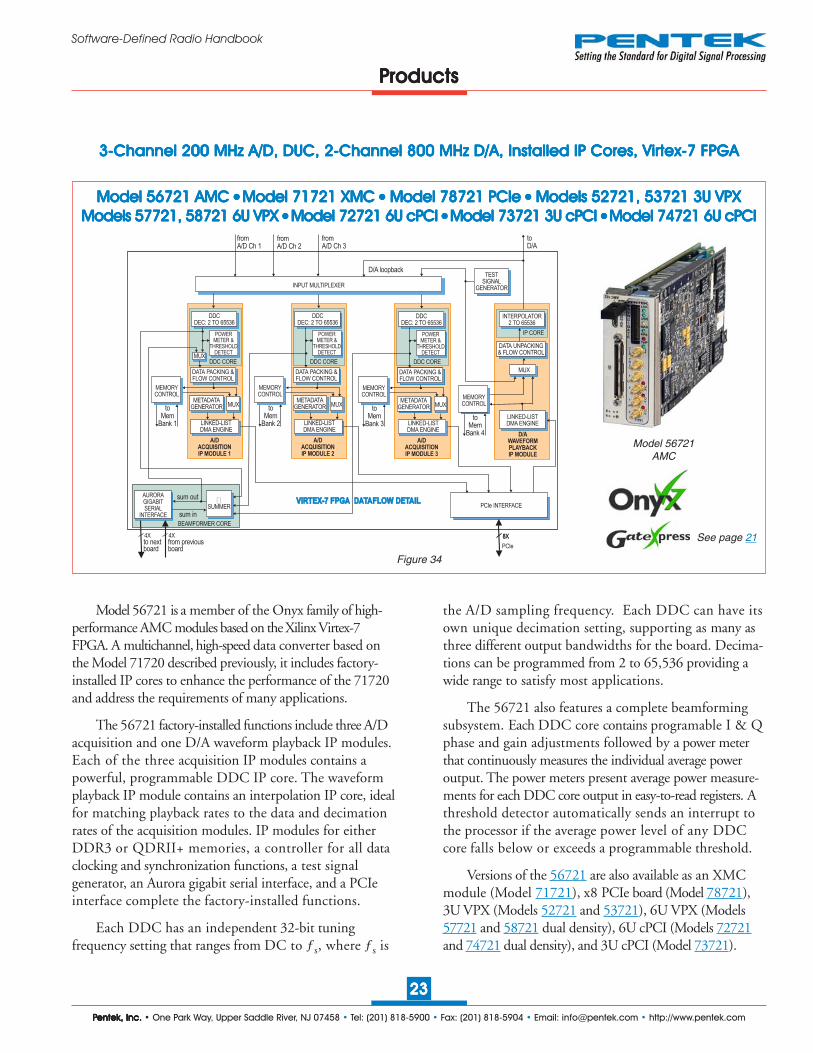
Model 71621 is a member of the Cobalt family of highperformance XMC modules based on the Xilinx Virtex-6FPGA. A multichannel, high-speed data converter based onthe Model 71620 described in the previous page, it includesfactory-installed IP cores to enhance the performance of the71620 and address the requirements of many applications.
The 71621 factory-installed functions include three A/Dacquisition and one D/A waveform playback IP modules.Each of the three acquisition IP modules contains apowerful, programmable DDC IP core. The waveformplayback IP module contains an interpolation IP core, idealfor matching playback rates to the data and decimationrates of the acquisition modules. IP modules for eitherDDR3 or QDRII+ memories, a controller for all dataclocking and synchronization functions, a test signalgenerator, an Aurora gigabit serial interface, and a PCIeinterface complete the factory-installed functions.
Each DDC has an independent 32-bit tuningfrequency setting that ranges from DC to ƒs, where ƒs is
the A/D sampling frequency. Each DDC can have itsown unique decimation setting, supporting as many asthree different output bandwidths for the board. Decima-tions can be programmed from 2 to 65,536 providing awide range to satisfy most applications.
The 71621 also features a complete beamformingsubsystem. Each DDC core contains programable I & Qphase and gain adjustments followed by a power meterthat continuously measures the individual average poweroutput. The power meters present average power measure-ments for each DDC core output in easy-to-read registers. Athreshold detector automatically sends an interrupt tothe processor if the average power level of any DDCcore falls below or exceeds a programmable threshold.
Versions of the 71621 are also available as an x8 PCIe half-length board (Model 78621), 3U VPX (Models 52621 and53621), 6U VPX (Models 57621 and 58621 dual density),AMC (Model 56621), 6U cPCI (Models 72621 and74621 dual density), and 3U cPCI (Model 73621).
PPPPPentek, Inc.entek, Inc.entek, Inc.entek, Inc.entek, Inc. • One Park Way, Upper Saddle River, NJ 07458 • Tel: (201) 818-5900 • Fax: (201) 818-5904 • Email: [email protected] • http://www.pentek.com
2323232323
Software-Defined Radio Handbook
PCIe INTERFACE
fromA/D Ch 1
fromA/D Ch 2
fromA/D Ch 3
PCIe
8Xfrom previousboard
to nextboard
sum out
sum in
VIRTEX-7 FPGA DATAFLOW DETAILVIRTEX-7 FPGA DATAFLOW DETAIL
A/DACQUISITIONIP MODULE 1
A/DACQUISITIONIP MODULE 2
A/DACQUISITIONIP MODULE 3
LINKED-LISTDMA ENGINE
LINKED-LISTDMA ENGINE
LINKED-LISTDMA ENGINE
METADATAGENERATOR
METADATAGENERATOR
METADATAGENERATORto
MemBank 1
MEMORYCONTROL
toMem
Bank 2
MEMORYCONTROL
toMem
Bank 3
MEMORYCONTROL
MUX MUX MUX
DATA PACKING &FLOW CONTROL
DATA PACKING &FLOW CONTROL
DATA PACKING &FLOW CONTROL
AURORAGIGABITSERIAL
INTERFACE
INPUT MULTIPLEXER
�SUMMER
DDCDEC: 2 TO 65536
DDCDEC: 2 TO 65536
BEAMFORMER CORE
DDCDEC: 2 TO 65536
POWERMETER &
THRESHOLDDETECT
POWERMETER &
THRESHOLDDETECT
POWERMETER &
THRESHOLDDETECT
MUXDDC CORE DDC CORE DDC CORE
D/AWAVEFORMPLAYBACKIP MODULE
toD/A
D/A loopbackTEST
SIGNALGENERATOR
MUX
LINKED-LISTDMA ENGINE
toMem
Bank 4
MEMORYCONTROL
DATA PACKING &FLOW CONTROL
DATA UNPACKING& FLOW CONTROL
INTERPOLATOR2 TO 65536
IP CORE
8X4X 4X
3-3-3-3-3-Channel 200 MHz A/D, DUC, 2-Channel 200 MHz A/D, DUC, 2-Channel 200 MHz A/D, DUC, 2-Channel 200 MHz A/D, DUC, 2-Channel 200 MHz A/D, DUC, 2-Channel 800 MHz D/A, Installed IP Cores, VirChannel 800 MHz D/A, Installed IP Cores, VirChannel 800 MHz D/A, Installed IP Cores, VirChannel 800 MHz D/A, Installed IP Cores, VirChannel 800 MHz D/A, Installed IP Cores, Virtex-7 FPGAtex-7 FPGAtex-7 FPGAtex-7 FPGAtex-7 FPGA
Model 56721 AMC Model 56721 AMC Model 56721 AMC Model 56721 AMC Model 56721 AMC ● ● ● ● ● Model 71721 XMC Model 71721 XMC Model 71721 XMC Model 71721 XMC Model 71721 XMC ●●●●● Model 78721 PCIe Model 78721 PCIe Model 78721 PCIe Model 78721 PCIe Model 78721 PCIe ●●●●● Models 52721, 53721 3U VPX Models 52721, 53721 3U VPX Models 52721, 53721 3U VPX Models 52721, 53721 3U VPX Models 52721, 53721 3U VPXModels 57721, 58721 6U VPX Models 57721, 58721 6U VPX Models 57721, 58721 6U VPX Models 57721, 58721 6U VPX Models 57721, 58721 6U VPX ●●●●● Model 72721 6U cPCI Model 72721 6U cPCI Model 72721 6U cPCI Model 72721 6U cPCI Model 72721 6U cPCI ● ● ● ● ● Model 73721 3U cPCI Model 73721 3U cPCI Model 73721 3U cPCI Model 73721 3U cPCI Model 73721 3U cPCI ● ● ● ● ● Model 74721 6U cPCIModel 74721 6U cPCIModel 74721 6U cPCIModel 74721 6U cPCIModel 74721 6U cPCI
Figure 34
PPPPProductsroductsroductsroductsroducts
Model 56721AMC
Model 56721 is a member of the Onyx family of high-performance AMC modules based on the Xilinx Virtex-7FPGA. A multichannel, high-speed data converter based onthe Model 71720 described previously, it includes factory-installed IP cores to enhance the performance of the 71720and address the requirements of many applications.
The 56721 factory-installed functions include three A/Dacquisition and one D/A waveform playback IP modules.Each of the three acquisition IP modules contains apowerful, programmable DDC IP core. The waveformplayback IP module contains an interpolation IP core, idealfor matching playback rates to the data and decimationrates of the acquisition modules. IP modules for eitherDDR3 or QDRII+ memories, a controller for all dataclocking and synchronization functions, a test signalgenerator, an Aurora gigabit serial interface, and a PCIeinterface complete the factory-installed functions.
Each DDC has an independent 32-bit tuningfrequency setting that ranges from DC to ƒs, where ƒs is
the A/D sampling frequency. Each DDC can have itsown unique decimation setting, supporting as many asthree different output bandwidths for the board. Decima-tions can be programmed from 2 to 65,536 providing awide range to satisfy most applications.
The 56721 also features a complete beamformingsubsystem. Each DDC core contains programable I & Qphase and gain adjustments followed by a power meterthat continuously measures the individual average poweroutput. The power meters present average power measure-ments for each DDC core output in easy-to-read registers. Athreshold detector automatically sends an interrupt tothe processor if the average power level of any DDCcore falls below or exceeds a programmable threshold.
Versions of the 56721 are also available as an XMCmodule (Model 71721), x8 PCIe board (Model 78721),3U VPX (Models 52721 and 53721), 6U VPX (Models57721 and 58721 dual density), 6U cPCI (Models 72721and 74721 dual density), and 3U cPCI (Model 73721).
See page 21

PPPPPentek, Inc.entek, Inc.entek, Inc.entek, Inc.entek, Inc. • One Park Way, Upper Saddle River, NJ 07458 • Tel: (201) 818-5900 • Fax: (201) 818-5904 • Email: [email protected] • http://www.pentek.com
2424242424
Software-Defined Radio Handbook
Models 52Models 52Models 52Models 52Models 52624624624624624, 53, 53, 53, 53, 53624624624624624 3U VPX 3U VPX 3U VPX 3U VPX 3U VPX ●●●●● MoMoMoMoModel 71del 71del 71del 71del 71624624624624624 XMC XMC XMC XMC XMC ●●●●● Model 78 Model 78 Model 78 Model 78 Model 78624624624624624 PCIe PCIe PCIe PCIe PCIe ●●●●● Model 56624 AMCModel 56624 AMCModel 56624 AMCModel 56624 AMCModel 56624 AMCModels 57Models 57Models 57Models 57Models 57624624624624624, 58, 58, 58, 58, 58624624624624624 6U VPX 6U VPX 6U VPX 6U VPX 6U VPX ●●●●● Model 72Model 72Model 72Model 72Model 72724724724724724 6U cPCI 6U cPCI 6U cPCI 6U cPCI 6U cPCI ●●●●● Model 73Model 73Model 73Model 73Model 73624624624624624 3U cPCI 3U cPCI 3U cPCI 3U cPCI 3U cPCI ● ● ● ● ● Model 74Model 74Model 74Model 74Model 74624624624624624 6U cPCI 6U cPCI 6U cPCI 6U cPCI 6U cPCI
Dual-Dual-Dual-Dual-Dual-Channel 34-Signal Adaptive IF RChannel 34-Signal Adaptive IF RChannel 34-Signal Adaptive IF RChannel 34-Signal Adaptive IF RChannel 34-Signal Adaptive IF Relayelayelayelayelay, Installed IP Cores, Vir, Installed IP Cores, Vir, Installed IP Cores, Vir, Installed IP Cores, Vir, Installed IP Cores, Virtex-6 FPGAtex-6 FPGAtex-6 FPGAtex-6 FPGAtex-6 FPGA
PPPPProductsroductsroductsroductsroducts
Figure 35
Model 52624 is a member of the Cobalt® family ofhigh-performance 3U OpenVPX boards based on theXilinx Virtex-6 FPGA. As an IF relay, it accepts two IFanalog input channels, modifies up to 34 signals, and thendelivers them to two analog IF outputs. Any signalwithin each IF band can be independently enabled ordisabled, and changed in both frequency and amplitudeas it passes through the board.
The 52624 supports many useful functions for bothcommercial and military communications systems includingsignal drop/add/replace, frequency shifting and hopping,amplitude equalization, and bandwidth consolidation.Applications include countermeasures, active tracking andmonitoring, channel security, interception, adaptivespectral management, jamming, and encryption.
The Pentek Cobalt product family features the Virtex-6FPGA. All of the board’s data converters, interfaces andcontrol lines are connected to the FPGA, which performsthe data-routing and DSP functions for the adaptive relay.
A PCIe Gen 1 system interface supports control, statusand data transfers.
The Model 52624 digitizes two analog IF inputsusing two 200 MHz 16-bit A/D converters. The band-width of each IF signal can be up to 80 MHz, and maycontain multiple signals, each centered at a differentfrequency. An array of 34 DDCs can be independentlyprogrammed to translate any signal to baseband andthen bandlimit the signal as required. DDC tuning frequencyis programmable from 0 Hz to the A/D sample rate. Outputbandwidth is programmable from around 20 kHz to 312 kHzfor a sample rate of 200 MHz. Each DDC can indepen-dently source IF data from either of the two A/Ds.
Versions of the 52624 are also available as a different3U VPX (Model 53624), 6U VPX (Models 57624 and58624 with dual density), XMC module (Model 71624),an x8 PCIe board (Model 78624), AMC (Model 56624),6U cPCI (Models 72624 and 74624 dual density), and 3UcPCI (Model 73624).
800 MHz16-BIT
D/A
IF 1Out
INTERPX4
TIMING BUSGENERATOR
Triggering/Clock / Sync /Gate / PPS VCXO
200 MHz16-BIT
A/D
INPUTGAIN 1
TTL Gate / TrigTTL Sync / PPS
Gate A/DGate D/A
Sync / PPS A/DSync / PPS D/A
Sample Clk /Reference Clk In
A/DClock/Sync Bus
IF 1In
DDC1
OUTPUTGAIN 1
DUC1
INP
UT
MU
LTIP
LEX
ER
INPUTGAIN 2
DDC2
OUTPUTGAIN 2
DUC2
INPUTGAIN 3
DDC3
OUTPUTGAIN 3
DUC3
INPUTGAIN 34
DDC34
OUTPUTGAIN 34
DUC34
OU
TP
UT
MU
LTIP
LEX
ER
200 MHz16-BIT
A/D
IF 2In
SU
MM
AT
ION
1S
UM
MA
TIO
N2
800 MHz16-BIT
D/A
IF 2Out
INTERPX4
TRANSMIT DMACONTROLLER
RECEIVE DMACONTROLLER
PCIeINTERFACE
STATUS &CONTROL
To AllSections
D/AClock/Sync Bus
VPX BACKPLANE
VPX-P1
PCIeGen. 1 x8
Model 52624 COTSand rugged

PPPPPentek, Inc.entek, Inc.entek, Inc.entek, Inc.entek, Inc. • One Park Way, Upper Saddle River, NJ 07458 • Tel: (201) 818-5900 • Fax: (201) 818-5904 • Email: [email protected] • http://www.pentek.com
2525252525
Software-Defined Radio Handbook
TIMING BUSGENERATOR
Clock / Sync /Gate / PPS D/A Clock/Sync Bus
VCXO
16
QDRII+SRAM8 MB
Gate InSync In
A/D Sync Bus
Sample Clk /Reference Clk In
A/D Clock/Sync Bus
16
16 16
ConfigFLASH64 MB
16
QDRII+SRAM8 MB
16
RFXFORMR
RF Out
RFXFORMR
DDR3SDRAM512 MB
DDR3SDRAM512 MB
QDRII+ option 150
16 1616 16
DDR3SDRAM512 MB
DDR3SDRAM512 MB
RF In
RFXFORMR
1 GHz12-BIT A/D
12
Memory Banks 1 & 2 Memory Banks 3 & 4DDR3 option 155 DDR3 option 165
Gate InSync In
D/A Sync Bus
1 GHz16-BIT D/A
TTLPPS/Gate/Sync
40 4X
GTX
4X
GTXLVDS GTX
OptionalFPGAGPIO
OptionalSerialI/O
8X
68-pinHeader
x8 PCI Express
Dual 4XSerialConn
x8 PCIe
VIRTEX-6 FPGA
LX130T, LX240T or SX315T
1 GHz A/D, 1 GHz D/A, Vir1 GHz A/D, 1 GHz D/A, Vir1 GHz A/D, 1 GHz D/A, Vir1 GHz A/D, 1 GHz D/A, Vir1 GHz A/D, 1 GHz D/A, Virtex-6 FPGAtex-6 FPGAtex-6 FPGAtex-6 FPGAtex-6 FPGA
Model 78630 PCIe Model 78630 PCIe Model 78630 PCIe Model 78630 PCIe Model 78630 PCIe ● ● ● ● ● Model 71630 XMC Model 71630 XMC Model 71630 XMC Model 71630 XMC Model 71630 XMC ●●●●● Model 52630, 53630 3U VPX Model 52630, 53630 3U VPX Model 52630, 53630 3U VPX Model 52630, 53630 3U VPX Model 52630, 53630 3U VPX ● ● ● ● ● Model 57630, 58630 6U VPXModel 57630, 58630 6U VPXModel 57630, 58630 6U VPXModel 57630, 58630 6U VPXModel 57630, 58630 6U VPXModel 56630 AMC Model 56630 AMC Model 56630 AMC Model 56630 AMC Model 56630 AMC ●●●●● Model 72630 6U cPCI Model 72630 6U cPCI Model 72630 6U cPCI Model 72630 6U cPCI Model 72630 6U cPCI ● ● ● ● ● Model 73630 3U cPCI Model 73630 3U cPCI Model 73630 3U cPCI Model 73630 3U cPCI Model 73630 3U cPCI ● ● ● ● ● Model 74630 6U cPCIModel 74630 6U cPCIModel 74630 6U cPCIModel 74630 6U cPCIModel 74630 6U cPCI
Figure 36
PPPPProductsroductsroductsroductsroducts
Model 78630x8 PCIe
Model 78630 is a member of the Cobalt family of highperformance PCIe boards based on the Xilinx Virtex-6FPGA. A high-speed data converter, it is suitable forconnection to HF or IF ports of a communications or radarsystem. Its built-in data capture and playback features offeran ideal turnkey solution as well as a platform for develop-ing and deploying custom FPGA processing IP. It includes1 GHz, 12-bit A/D, 1 GHz, 16-bit D/A converters andfour banks of memory. In addition to supporting PCIExpress Gen. 2 as a native interface, the Model 78630includes optional general purpose and gigabit serial cardconnectors for application- specific I/O protocols.
The Pentek Cobalt architecture features a Virtex-6FPGA. All of the board’s data and control paths are acces-sible by the FPGA, enabling factory-installed functionsincluding data multiplexing, channel selection, data packing,gating, triggering and memory control. The Cobalt architec-ture organizes the FPGA as a container for data process-ing applications where each function exists as an intellec-tual property (IP) module.
Each member of the Cobalt family is deliveredwith factory-installed applications ideally matched to theboard’s analog interfaces. The 78630 factory-installedfunctions include an A/D acquisition and a D/A waveformplayback IP module. In addition, IP modules for eitherDDR3 or QDRII+ memories, a controller for all dataclocking and synchronization functions, a test signalgenerator and a PCIe interface complete the factory-installed functions.
Multiple 78630’s can be driven from the LVPECL busmaster, supporting synchronous sampling and sync functionsacross all connected boards. The architecture supports up tofour memory banks which can be configured with allQDRII+ SRAM, DDR3 SDRAM, or as combinations.
Versions of the 78630 are also available as an XMCmodule (Model 71630), 3U VPX (Models 52630 and53630), 6U VPX (Models 57630 and 58630 with dualdensity), AMC (Model 56630), 6U cPCI (Models 72630and 74630 with dual density), and 3U cPCI (Model 73630).

PPPPPentek, Inc.entek, Inc.entek, Inc.entek, Inc.entek, Inc. • One Park Way, Upper Saddle River, NJ 07458 • Tel: (201) 818-5900 • Fax: (201) 818-5904 • Email: [email protected] • http://www.pentek.com
2626262626
Software-Defined Radio Handbook
1 GHz A/D, 1 GHz D/A, Vir1 GHz A/D, 1 GHz D/A, Vir1 GHz A/D, 1 GHz D/A, Vir1 GHz A/D, 1 GHz D/A, Vir1 GHz A/D, 1 GHz D/A, Virtex-7 FPGAtex-7 FPGAtex-7 FPGAtex-7 FPGAtex-7 FPGA
Model 71730 XMC Model 71730 XMC Model 71730 XMC Model 71730 XMC Model 71730 XMC ●●●●● Model 78730 PCIe Model 78730 PCIe Model 78730 PCIe Model 78730 PCIe Model 78730 PCIe ● ● ● ● ● Model 52730, 53730 3U VPX Model 52730, 53730 3U VPX Model 52730, 53730 3U VPX Model 52730, 53730 3U VPX Model 52730, 53730 3U VPX ● ● ● ● ● Model 57730, 58630 6U VPXModel 57730, 58630 6U VPXModel 57730, 58630 6U VPXModel 57730, 58630 6U VPXModel 57730, 58630 6U VPXModel 56730 AMC Model 56730 AMC Model 56730 AMC Model 56730 AMC Model 56730 AMC ●●●●● Model 72730 6U cPCI Model 72730 6U cPCI Model 72730 6U cPCI Model 72730 6U cPCI Model 72730 6U cPCI ● ● ● ● ● Model 73730 3U cPCI Model 73730 3U cPCI Model 73730 3U cPCI Model 73730 3U cPCI Model 73730 3U cPCI ● ● ● ● ● Model 74730 6U cPCIModel 74730 6U cPCIModel 74730 6U cPCIModel 74730 6U cPCIModel 74730 6U cPCI
Figure 37
PPPPProductsroductsroductsroductsroducts
Model 71730XMC
TIMING BUSGENERATOR
Clock / Sync /Gate / PPS D/A Clock/Sync Bus
VCXO
Gate InSync In
A/D Sync Bus
Sample Clk /Reference Clk In
A/D Clock/Sync Bus
16
RFXFORMR
RF Out
RFXFORMR
RF In
RFXFORMR
1 GHz12-BIT A/D
12Gate InSync In
D/A Sync Bus
1 GHz16-BIT D/A
TTLPPS/Gate/Sync
VIRTEX-7 FPGA
VX330T or VX690T
GigabitSerial I/O(option 105)
GTXGTX LVDSGTX
FPGAGPIO(option 104)
PCIeGen. 3 x8
P14PMC
P16XMC
P15XMC
4X4XCONFIGFLASH1 GB
DDR3SDRAM
1 GB
DDR3SDRAM
1 GB
DDR3SDRAM
1 GB
DDR3SDRAM
1 GB
48 32 32 32 32PCIeGen. 3 x8
FPGAConfigBus
GATEXPRESS PCIeCONFIGURATION
MANAGER
Model 71730 is a member of the Onyx family of highperformance XMC modules based on the Xilinx Virtex-7FPGA. A high-speed data converter, it is suitable forconnection to HF or IF ports of a communications orradar system. Its built-in data capture and playback featuresoffer an ideal turnkey solution as well as a platform fordeveloping and deploying custom FPGA processing IP.It includes 1 GHz A/D and D/A converters and fourbanks of memory. In addition to supporting PCIExpress Gen. 3 as a native interface, the Model 71730includes optional general purpose and gigabit serial cardconnectors for application-specific I/O.
The Pentek Onyx architecture features a Virtex-7FPGA. All of the board’s data and control paths areaccessible by the FPGA, enabling factory-installedfunctions including data multiplexing, channel selection,data packing, gating, triggering and memory control. TheOnyx architecture organizes the FPGA as a container fordata processing applications where each function existsas an intellectual property (IP) module.
Each member of the Onyx family is delivered withfactory-installed applications ideally matched to theboard’s analog interfaces. The 71730 factory-installedfunctions include an A/D acquisition and a D/A waveformplayback IP module for simplifying data capture anddata transfer. IP modules for DDR3 SDRAM memories, acontroller for all data clocking and synchronization functions,a test signal generator and a PCIe interface complete thefactory-installed functions and enable the 71730 tooperate without the need to develop any FPGA IP.
The front end accepts an analog HF or IF input on a frontpanel SSMC connector with transformer coupling into a TIADS5400 1 GHz, 12-bit A/D converter. The digital outputsare delivered into the Virtex-7 FPGA for signal processing, etc.
Versions of the 71730 are also available as an x8 PCIehalf-length board (Model 78730), 3U VPX (Models 52730and 53730), 6U VPX (Models 57730 and 58730 dualdensity), AMC (Model 56730), 6U cPCI (Models 72730and 74730 with dual density), and 3U cPCI (Model 73730).
See page 21

PPPPPentek, Inc.entek, Inc.entek, Inc.entek, Inc.entek, Inc. • One Park Way, Upper Saddle River, NJ 07458 • Tel: (201) 818-5900 • Fax: (201) 818-5904 • Email: [email protected] • http://www.pentek.com
2727272727
Software-Defined Radio Handbook
Figure 38
PPPPProductsroductsroductsroductsroducts
TIMING BUSGENERATOR
Clock / Sync /Gate / PPS
32
Gate In
Reset In
Sync Bus
Sample Clk
A/D Clock/Sync Bus
16
ConfigFLASH64 MB
32
DDR3SDRAM512 MB
DDR3SDRAM512 MB
3232
DDR3SDRAM512 MB
DDR3SDRAM512 MB
RF In
RFXFORMR
3.6 GHz (1 Channel)or
1.8 GHz (2 Channel)12-bit A/D
12
Memory Banks 1 & 2 Memory Banks 3 & 4
TTLPPS/Gate/Sync
RF In
RFXFORMR
Ref Clk In
Ref Clk Out 12
Block Diagram, Model 72640
Model 74640 doubles all resources
except the PCI-to-PCI Bridge
VIRTEX-6 FPGA
MODEL 73640
INTERFACES ONLY
PCIeto PCI
BRIDGE
40
LVDS GTX
OptionalFPGA I/O(Option -104)
PCI/PCI-X BUS32-bit, 33/66 MHz
J2
PCIeto PCI
BRIDGE
PCIto PCI
BRIDGE
From/To OtherXMC Module ofMODEL 74640
GTX
x4 PCIe
PCI/PCI-X BUS32/64-bit, 33/66 MHz
4X40
LVDS
OptionalFPGA I/O(Option -104)
J3
VIRTEX-6 FPGA
LX130T, LX240T or SX315T
Model 74640Dual Density
Model 73640Single Density
Model 72640 6U cPCI Model 72640 6U cPCI Model 72640 6U cPCI Model 72640 6U cPCI Model 72640 6U cPCI ● ● ● ● ● Model 73640 3U cPCI Model 73640 3U cPCI Model 73640 3U cPCI Model 73640 3U cPCI Model 73640 3U cPCI ● ● ● ● ● Model 74640 6U cPCI Model 74640 6U cPCI Model 74640 6U cPCI Model 74640 6U cPCI Model 74640 6U cPCI ● ● ● ● ● Model 71640 XMCModel 71640 XMCModel 71640 XMCModel 71640 XMCModel 71640 XMCModel 78640 PCIe Model 78640 PCIe Model 78640 PCIe Model 78640 PCIe Model 78640 PCIe ●●●●● Models 52640, 53640 3U VPX Models 52640, 53640 3U VPX Models 52640, 53640 3U VPX Models 52640, 53640 3U VPX Models 52640, 53640 3U VPX ●●●●● Models 57640,Models 57640,Models 57640,Models 57640,Models 57640, 58640 6U VPX 58640 6U VPX 58640 6U VPX 58640 6U VPX 58640 6U VPX ●●●●● Model 56640 AMC Model 56640 AMC Model 56640 AMC Model 56640 AMC Model 56640 AMC
1- or 2-1- or 2-1- or 2-1- or 2-1- or 2-Channel 3.6 GHz and 2- or 4-Channel 3.6 GHz and 2- or 4-Channel 3.6 GHz and 2- or 4-Channel 3.6 GHz and 2- or 4-Channel 3.6 GHz and 2- or 4-Channel 1.8 GHz, 12-bit A/D, VirChannel 1.8 GHz, 12-bit A/D, VirChannel 1.8 GHz, 12-bit A/D, VirChannel 1.8 GHz, 12-bit A/D, VirChannel 1.8 GHz, 12-bit A/D, Virtex-6 FPGAtex-6 FPGAtex-6 FPGAtex-6 FPGAtex-6 FPGA
Models 72640, 73640 and 74640 are membersof the Cobalt family of high performance CompactPCIboards based on the Xilinx Virtex-6 FPGA. Theyconsist of one or two Model 71640 XMC modulesmounted on a cPCI carrier board. These models include oneor two 3.6 GHz, 12-bit A/D converters and four or eightbanks of memory.
The Pentek Cobalt architecture features a Virtex-6FPGA. All of the board’s data and control paths areaccessible by the FPGA, enabling factory-installedfunctions including data multiplexing, channel selec-tion, data packing, gating, triggering and memory control.The Cobalt architecture organizes the FPGA as a containerfor data processing applications where each function existsas an intellectual property (IP) module.
Each member of the Cobalt family is deliveredwith factory-installed applications ideally matched to theboard’s analog interfaces. The factory-installed functions ofthese models include one or two A/D acquisition IP
modules. In addition, IP modules for DDR3 memories,controllers for all data clocking and synchronizationfunctions, a test signal generator and a PCIe interfacecomplete the factory-installed functions.
The front end accepts analog HF or IF inputs ona pair of front panel SSMC connectors with transformercoupling into a Texas Instruments ADC12D1800 12-bitA/D. The converter operates in single-channel interleavedmode with a sampling rate of 3.6 GHz and an inputbandwidth of 1.75 GHz; or, in dual-channel mode with asampling rate of 1.8 GHz and input bandwidth of 2.8GHz. The ADC12D1800 provides a programmable 15-bitgain adjustment allowing an input range of +2 to +4 dBm.
Model 72640 is a 6U cPCI board, while Model 73640is a 3U cPCI board; Model 74640 isa dual density 6UcPCI board; also available are an XMC (Model 71640),x8 PCIe (Model 78640), 3U VPX (Models 52640 and53640), 6U VPX (Models 57640 and 58640 dual density),and AMC (Model 56640).

PPPPPentek, Inc.entek, Inc.entek, Inc.entek, Inc.entek, Inc. • One Park Way, Upper Saddle River, NJ 07458 • Tel: (201) 818-5900 • Fax: (201) 818-5904 • Email: [email protected] • http://www.pentek.com
2828282828
Software-Defined Radio Handbook
Figure 39
PPPPProductsroductsroductsroductsroducts
Model 56641 AMC Model 56641 AMC Model 56641 AMC Model 56641 AMC Model 56641 AMC ●●●●● Model 71641 XMC Model 71641 XMC Model 71641 XMC Model 71641 XMC Model 71641 XMC ●●●●● Model 78641 PCIe Model 78641 PCIe Model 78641 PCIe Model 78641 PCIe Model 78641 PCIe ●●●●● Models 52641, 53641 3U VPX Models 52641, 53641 3U VPX Models 52641, 53641 3U VPX Models 52641, 53641 3U VPX Models 52641, 53641 3U VPXModels 57641, 58641 6U VPX Models 57641, 58641 6U VPX Models 57641, 58641 6U VPX Models 57641, 58641 6U VPX Models 57641, 58641 6U VPX ●●●●● Model 72641 6U cPCI Model 72641 6U cPCI Model 72641 6U cPCI Model 72641 6U cPCI Model 72641 6U cPCI ● ● ● ● ● Model 73641 3U cPCI Model 73641 3U cPCI Model 73641 3U cPCI Model 73641 3U cPCI Model 73641 3U cPCI ● ● ● ● ● Model 74641 6U cPCIModel 74641 6U cPCIModel 74641 6U cPCIModel 74641 6U cPCIModel 74641 6U cPCI
1- Channel 3.6 GHz or 2-1- Channel 3.6 GHz or 2-1- Channel 3.6 GHz or 2-1- Channel 3.6 GHz or 2-1- Channel 3.6 GHz or 2-Channel 1.8 GHz, 12-bit A/D, WChannel 1.8 GHz, 12-bit A/D, WChannel 1.8 GHz, 12-bit A/D, WChannel 1.8 GHz, 12-bit A/D, WChannel 1.8 GHz, 12-bit A/D, Wideband DDC, Virideband DDC, Virideband DDC, Virideband DDC, Virideband DDC, Virtex-6 FPGAtex-6 FPGAtex-6 FPGAtex-6 FPGAtex-6 FPGA
PCIe INTERFACE
fromA/D
PCIeFPGAGPIO
VIRTEX-6 FPGA DATAFLOW DETAILVIRTEX-6 FPGA DATAFLOW DETAIL
A/DACQUISITIONIP MODULE
MUX
INPUT MULTIPLEXERTEST
SIGNALGENERATOR
MEMORYCONTROLLER
8X 40toMem
Bank 2
toMem
Bank 1
fromA/D
LINKED-LISTDMA ENGINE
toMEM
CONTROL
MEMORYCONTROLLER
toMem
Bank 4
toMem
Bank 3
*Two channel mode shown.Programmable decimation of 8, 16 or 32
available in one channel mode.
DDC*DEC: 4, 8 or 16
POWERMETER &
THRESHOLDDETECT
DDC CORE
DATA PACKING &FLOW CONTROL
A/DACQUISITIONIP MODULE
MUX
LINKED-LISTDMA ENGINE
DDC*DEC: 4, 8 or 16
POWERMETER &
THRESHOLDDETECT
DDC CORE
DATA PACKING &FLOW CONTROL
METADATAGENERATOR
METADATAGENERATOR
Model 56641AMC
Model 56641 is a member of the Cobalt family of highperformance AMC modules based on the Xilinx Virtex-6FPGA. A very high-speed data converter based on the Model56640 described in the previous page, it includes additionalfactory-installed IP cores to enhance the performance of the56640 and address the requirements of many applications.
The 56641 factory-installed functions include an A/Dacquisition IP module. In addition, within the FPGA isa powerful factory-installed DDC IP core. The coresupports a single-channel mode, accepting data samplesfrom the A/D at the full 3.6 GHz rate. Additionally, adual-channel mode supports the A/D’s 1.8 GHz two-channel operation .
In dual-channel mode, each DDC has an indepen-dent 32-bit tuning frequency setting that ranges fromDC to ƒs, where ƒs is the A/D sampling frequency.
In single-channel mode, decimation can be programmedto 8x, 16x or 32x. In dual-channel mode, both channelsshare the same decimation rate, programmable to 4x, 8xor 16x.
The decimating filter for each DDC accepts aunique set of user-supplied 16-bit coefficients. The 80%default filters deliver an output bandwidth of 0.8*ƒs/N,where N is the decimation setting. The rejection ofadjacent-band components within the 80% outputbandwidth is better than 100 dB. Each DDC delivers acomplex output stream consisting of 16-bit I + 16-bit Qsamples at a rate of ƒs/N.
Versions of the 56641 are also available as an XMCmodule (Model 71641), x8 PCIe board (Model 78641),3U VPX (Models 52641 and 53641), 6U VPX (Models57641 and 58641 dual density), 6U cPCI (Models 72641and 74641 dual density), and 3U cPCI (Model 73641).
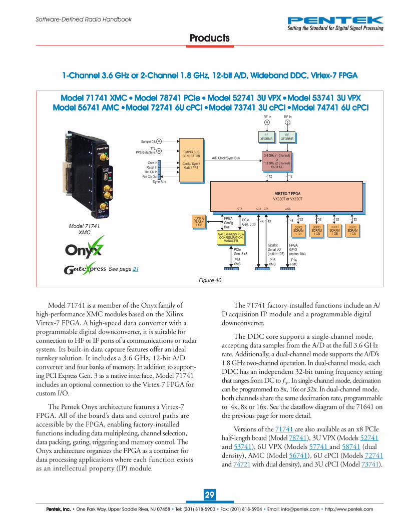
PPPPPentek, Inc.entek, Inc.entek, Inc.entek, Inc.entek, Inc. • One Park Way, Upper Saddle River, NJ 07458 • Tel: (201) 818-5900 • Fax: (201) 818-5904 • Email: [email protected] • http://www.pentek.com
2929292929
Software-Defined Radio Handbook
PPPPProductsroductsroductsroductsroducts
Model 71741 XMC Model 71741 XMC Model 71741 XMC Model 71741 XMC Model 71741 XMC ●●●●● Model 78741 PCIe Model 78741 PCIe Model 78741 PCIe Model 78741 PCIe Model 78741 PCIe ●●●●● Model 52741 3U VPX Model 52741 3U VPX Model 52741 3U VPX Model 52741 3U VPX Model 52741 3U VPX ● ● ● ● ● Model 53741 3U VPXModel 53741 3U VPXModel 53741 3U VPXModel 53741 3U VPXModel 53741 3U VPX Model 56741 AMC Model 56741 AMC Model 56741 AMC Model 56741 AMC Model 56741 AMC ● ● ● ● ● Model 72741 6U cPCI Model 72741 6U cPCI Model 72741 6U cPCI Model 72741 6U cPCI Model 72741 6U cPCI ● ● ● ● ● Model 73741 3U cPCI Model 73741 3U cPCI Model 73741 3U cPCI Model 73741 3U cPCI Model 73741 3U cPCI ● ● ● ● ● Model 74741 6U cPCIModel 74741 6U cPCIModel 74741 6U cPCIModel 74741 6U cPCIModel 74741 6U cPCI
1-1-1-1-1-Channel 3.6 GHz or 2-Channel 3.6 GHz or 2-Channel 3.6 GHz or 2-Channel 3.6 GHz or 2-Channel 3.6 GHz or 2-Channel 1.8 GHz, 12-bit A/D, WChannel 1.8 GHz, 12-bit A/D, WChannel 1.8 GHz, 12-bit A/D, WChannel 1.8 GHz, 12-bit A/D, WChannel 1.8 GHz, 12-bit A/D, Wideband DDC, Virideband DDC, Virideband DDC, Virideband DDC, Virideband DDC, Virtex-7 FPGAtex-7 FPGAtex-7 FPGAtex-7 FPGAtex-7 FPGA
Figure 40
Model 71741XMC
TIMING BUSGENERATOR
Clock / Sync /Gate / PPS
Gate In
Reset In
Sync Bus
Sample Clk
A/D Clock/Sync Bus
RF In
RFXFORMR
3.6 GHz (1 Channel)or
1.8 GHz (2 Channel)12-Bit A/D
12
TTLPPS/Gate/Sync
RF In
RFXFORMR
Ref Clk In
Ref Clk Out 12
VIRTEX-7 FPGA
VX330T or VX690T
GTX
PCIeGen. 3 x8
P15XMC
CONFIGFLASH1 GB
DDR3SDRAM
1 GB
DDR3SDRAM
1 GB
DDR3SDRAM
1 GB
DDR3SDRAM
1 GB
32 32 32 32PCIeGen. 3 x8
FPGAConfigBus
GATEXPRESS PCIeCONFIGURATION
MANAGER
GigabitSerial I/O(option 105)
GTXGTX LVDS
FPGAGPIO(option 104)
P14PMC
P16XMC
4X4X 48
Model 71741 is a member of the Onyx family ofhigh-performance XMC modules based on the XilinxVirtex-7 FPGA. A high-speed data converter with aprogrammable digital downconverter, it is suitable forconnection to HF or IF ports of a communications or radarsystem. Its built-in data capture features offer an idealturnkey solution. It includes a 3.6 GHz, 12-bit A/Dconverter and four banks of memory. In addition to support-ing PCI Express Gen. 3 as a native interface, Model 71741includes an optional connection to the Virtex-7 FPGA forcustom I/O.
The Pentek Onyx architecture features a Virtex-7FPGA. All of the board’s data and control paths areaccessible by the FPGA, enabling factory-installedfunctions including data multiplexing, channel selection,data packing, gating, triggering and memory control. TheOnyx architecture organizes the FPGA as a container fordata processing applications where each function existsas an intellectual property (IP) module.
The 71741 factory-installed functions include an A/D acquisition IP module and a programmable digitaldownconverter.
The DDC core supports a single-channel mode,accepting data samples from the A/D at the full 3.6 GHzrate. Additionally, a dual-channel mode supports the A/D’s1.8 GHz two-channel operation. In dual-channel mode, eachDDC has an independent 32-bit tuning frequency settingthat ranges from DC to ƒs,. In single-channel mode, decimationcan be programmed to 8x, 16x or 32x. In dual-channel mode,both channels share the same decimation rate, programmableto 4x, 8x or 16x. See the dataflow diagram of the 71641 onthe previous page for more detail.
Versions of the 71741 are also available as an x8 PCIehalf-length board (Model 78741), 3U VPX (Models 52741and 53741), 6U VPX (Models 57741 and 58741 (dualdensity), AMC (Model 56741), 6U cPCI (Models 72741and 74721 with dual density), and 3U cPCI (Model 73741).
See page 21
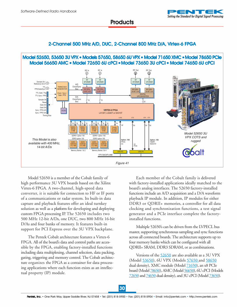
PPPPPentek, Inc.entek, Inc.entek, Inc.entek, Inc.entek, Inc. • One Park Way, Upper Saddle River, NJ 07458 • Tel: (201) 818-5900 • Fax: (201) 818-5904 • Email: [email protected] • http://www.pentek.com
3030303030
Software-Defined Radio Handbook
2-2-2-2-2-Channel 500 MHz A/D, DUC, 2-Channel 500 MHz A/D, DUC, 2-Channel 500 MHz A/D, DUC, 2-Channel 500 MHz A/D, DUC, 2-Channel 500 MHz A/D, DUC, 2-Channel 800 MHz D/A, VirChannel 800 MHz D/A, VirChannel 800 MHz D/A, VirChannel 800 MHz D/A, VirChannel 800 MHz D/A, Virtex-6 FPGAtex-6 FPGAtex-6 FPGAtex-6 FPGAtex-6 FPGA
Model 52650, 53650 3U VPX Model 52650, 53650 3U VPX Model 52650, 53650 3U VPX Model 52650, 53650 3U VPX Model 52650, 53650 3U VPX ●●●●● Models 57650, 58650 6U VPX Models 57650, 58650 6U VPX Models 57650, 58650 6U VPX Models 57650, 58650 6U VPX Models 57650, 58650 6U VPX ●●●●● Model 71650 XMC Model 71650 XMC Model 71650 XMC Model 71650 XMC Model 71650 XMC ● ● ● ● ● Model 78650 PCIeModel 78650 PCIeModel 78650 PCIeModel 78650 PCIeModel 78650 PCIeModel 56650 AMC Model 56650 AMC Model 56650 AMC Model 56650 AMC Model 56650 AMC ●●●●● Model 72650 6U cPCI Model 72650 6U cPCI Model 72650 6U cPCI Model 72650 6U cPCI Model 72650 6U cPCI ● ● ● ● ● Model 73650 3U cPCI Model 73650 3U cPCI Model 73650 3U cPCI Model 73650 3U cPCI Model 73650 3U cPCI ●●●●● Model 74650 6U cPCI Model 74650 6U cPCI Model 74650 6U cPCI Model 74650 6U cPCI Model 74650 6U cPCI
Figure 41
Model 52650 3UVPX COTS and
rugged
PPPPProductsroductsroductsroductsroducts
D/AClock/Sync
Bus
VCXO
500 MHz12-BIT A/D
RF In
RFXFORMR
RF In
RFXFORMR
16
QDRII+SRAM8 MB
TTL Gate / Trig
TTL Sync / PPS
Sample Clk
Reset
Gate A/D
Gate D/A
Sync / PPS A/D
Sync / PPS D/A
Timing Bus
500 MHz12-BIT A/D
Sample Clk /Reference Clk In A/D
Clock/SyncBus 800 MHz
16-BIT D/A
RFXFORMR
321616
RF Out
RFXFORMR
16 16
ConfigFLASH64 MB
16
QDRII+SRAM8 MB
16
RFXFORMR
RF Out
RFXFORMR
800 MHz16-BIT D/A
DIGITALUPCONVERTER
DDR3SDRAM512 MB
DDR3SDRAM512 MB
QDRII+ option 150
16
QDRII+SRAM8 MB
1616
QDRII+SRAM8 MB
16
DDR3SDRAM512 MB
DDR3SDRAM512 MB
Memory Banks 1 & 2 Memory Banks 3 & 4
DDR3 option 155
QDRII+ option 160
DDR3 option 165
TTLPPS/Gate/Sync
TIMING BUSGENERATOR
Clock / Sync /Gate / PPS
LVDS
40
FPGAI/O
Option -104
VPX BACKPLANE
VPX-P2 VPX-P1
VIRTEX-6 FPGA
LX130T, LX240T or SX315T
GTXGTXGTX
GigabitSerial I/O
Option -105
4X4X 4X
x4PCIe
Model 52650 is a member of the Cobalt family ofhigh performance 3U VPX boards based on the XilinxVirtex-6 FPGA. A two-channel, high-speed dataconverter, it is suitable for connection to HF or IF portsof a communications or radar system. Its built-in datacapture and playback features offer an ideal turnkeysolution as well as a platform for developing and deployingcustom FPGA processing IP. The 52650 includes two500 MHz 12-bit A/Ds, one DUC, two 800 MHz 16-bitD/As and four banks of memory. It features built-insupport for PCI Express over the 3U VPX backplane.
The Pentek Cobalt architecture features a Virtex-6FPGA. All of the board’s data and control paths are acces-sible by the FPGA, enabling factory-installed functionsincluding data multiplexing, channel selection, data packing,gating, triggering and memory control. The Cobalt architec-ture organizes the FPGA as a container for data process-ing applications where each function exists as an intellec-tual property (IP) module.
Each member of the Cobalt family is deliveredwith factory-installed applications ideally matched to theboard’s analog interfaces. The 52650 factory-installedfunctions include an A/D acquisition and a D/A waveformplayback IP module. In addition, IP modules for eitherDDR3 or QDRII+ memories, a controller for all dataclocking and synchronization functions, a test signalgenerator and a PCIe interface complete the factory-installed functions.
Multiple 52650’s can be driven from the LVPECL busmaster, supporting synchronous sampling and sync functionsacross all connected boards. The architecture supports up tofour memory banks which can be configured with allQDRII+ SRAM, DDR3 SDRAM, or as combinations.
Versions of the 52650 are also available as a 3U VPX(Model 53650), 6U VPX (Models 57650 and 58650dual density), XMC module (Model 71650), an x8 PCIeboard (Model 78650), AMC (Model 56650), 6U cPCI (Models72650 and 74650 dual density), and 3U cPCI (Model 73650).
This Model is alsoavailable with 400 MHz,
14-bit A/Ds

PPPPPentek, Inc.entek, Inc.entek, Inc.entek, Inc.entek, Inc. • One Park Way, Upper Saddle River, NJ 07458 • Tel: (201) 818-5900 • Fax: (201) 818-5904 • Email: [email protected] • http://www.pentek.com
3131313131
Software-Defined Radio Handbook
Model 72651 6U cPCI Model 72651 6U cPCI Model 72651 6U cPCI Model 72651 6U cPCI Model 72651 6U cPCI ● ● ● ● ● Model 73651 3U cPCI Model 73651 3U cPCI Model 73651 3U cPCI Model 73651 3U cPCI Model 73651 3U cPCI ● ● ● ● ● Model 74651 6U cPCI Model 74651 6U cPCI Model 74651 6U cPCI Model 74651 6U cPCI Model 74651 6U cPCI ● ● ● ● ● Model 52651 3U VPXModel 52651 3U VPXModel 52651 3U VPXModel 52651 3U VPXModel 52651 3U VPXModel 53651 3U VPX Model 53651 3U VPX Model 53651 3U VPX Model 53651 3U VPX Model 53651 3U VPX ● ● ● ● ● Model 71651 XMC Model 71651 XMC Model 71651 XMC Model 71651 XMC Model 71651 XMC ●●●●● Model 78651 PCIe Model 78651 PCIe Model 78651 PCIe Model 78651 PCIe Model 78651 PCIe ●●●●● Model 56651 AMC Model 56651 AMC Model 56651 AMC Model 56651 AMC Model 56651 AMC
PPPPProductsroductsroductsroductsroducts
2- or 4-2- or 4-2- or 4-2- or 4-2- or 4-Channel 500 MHz A/D, with DDCs, DUCs, 2- or 4-Channel 500 MHz A/D, with DDCs, DUCs, 2- or 4-Channel 500 MHz A/D, with DDCs, DUCs, 2- or 4-Channel 500 MHz A/D, with DDCs, DUCs, 2- or 4-Channel 500 MHz A/D, with DDCs, DUCs, 2- or 4-Channel 800 MHz D/A, VirChannel 800 MHz D/A, VirChannel 800 MHz D/A, VirChannel 800 MHz D/A, VirChannel 800 MHz D/A, Virtex-6 FPGAtex-6 FPGAtex-6 FPGAtex-6 FPGAtex-6 FPGA
Figure 42
PCIe INTERFACE
fromA/D Ch 1
fromA/D Ch 2
PCIe
4Xfrom previousboard
to nextboard
sum out
sum in
VIRTEX-6 FPGA DATAFLOW DETAILVIRTEX-6 FPGA DATAFLOW DETAIL
A/DACQUISITIONIP MODULE 1
A/DACQUISITIONIP MODULE 2
LINKED-LISTDMA ENGINE
LINKED-LISTDMA ENGINE
METADATAGENERATOR
METADATAGENERATORto
MemBank 1
MEMORYCONTROL
toMem
Bank 2
MEMORYCONTROL
MUX MUX
DATA PACKING &FLOW CONTROL
DATA PACKING &FLOW CONTROL
AURORAGIGABITSERIAL
INTERFACE
INPUT MULTIPLEXER
�SUMMER
DDCDEC: 2 TO 131027
DDCDEC: 2 TO 131027
BEAMFORMER CORE
POWERMETER &
THRESHOLDDETECT
POWERMETER &
THRESHOLDDETECT
MUXDDC CORE DDC CORE
D/AWAVEFORMPLAYBACKIP MODULE
toD/A
D/A loopbackTEST
SIGNALGENERATOR
MUX
LINKED-LISTDMA ENGINE
toMem
Bank 4
MEMORYCONTROL
DATA UNPACKING& FLOW CONTROL
INTERPOLATOR2 TO 65536
IP CORE
4X 4X
Model 74651Dual Density
Model 73651Single Density
Models 72651, 73651 and 74651 are members ofthe Cobalt family of high performance CompactPCI boardsbased on the Xilinx Virtex-6 FPGA. They consist ofone or two Model 71651 XMC modules mounted on acPCI carrier board. These models include two or four A/Ds,two or four multiband DDCs, one ot two DUCs, twoor four D/As and three or six banks of memory.
These models feature two or four A/D Acquisition IPmodules for easily capturing and moving data. Eachmodule can receive data from either of the two A/Ds, atest signal generator or from the D/A Waveform PlaybackIP module in loopback mode.
Within each A/D Acquisition IP Module is apowerful DDC IP core. Because of the flexible inputrouting of the A/D Acquisition IP Modules, many differentconfigurations can be achieved including one A/D drivingboth DDCs or each of the two A/Ds driving its own DDC.
Each DDC has an independent 32-bit tuningfrequency setting that ranges from DC to ƒs, where ƒs is
the A/D sampling frequency. Each DDC can have itsown unique decimation setting, supporting as many astwo or four different output bandwidths for the board.Decimations can be programmed from 2 to 131,072providing a wide range to satisfy most applications.
In addition to the DDCs, these models feature oneor two complete beamforming subsystems. Each DDCcore contains programable I & Q phase and gain adjust-ments followed by a power meter that continuouslymeasures the individual average power output. The timeconstant of the averaging interval for each meter is program-mable up to 8K samples. The power meters present averagepower measurements for each DDC core output.
Model 72651 is a 6U cPCI board, while Model 73651is a 3U cPCI board; Model 74651 a dual density 6U cPCIboard; also available are an XMC (Model 71651), an x8PCIe (Model 78651), 3U VPX (Models 52651 and 53651),6U VPX (Models 57651 and 58651 dual density), andAMC (Model 56651).
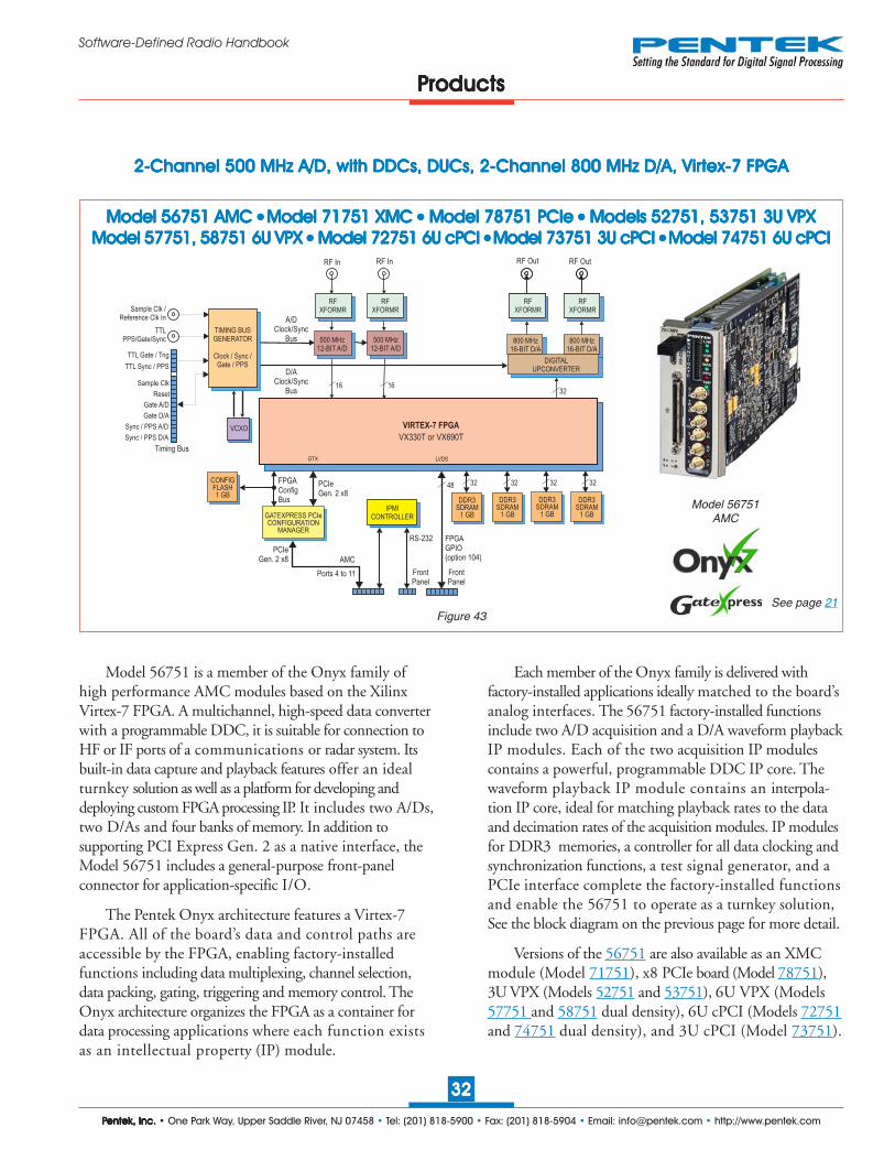
PPPPPentek, Inc.entek, Inc.entek, Inc.entek, Inc.entek, Inc. • One Park Way, Upper Saddle River, NJ 07458 • Tel: (201) 818-5900 • Fax: (201) 818-5904 • Email: [email protected] • http://www.pentek.com
3232323232
Software-Defined Radio Handbook
Model 56751 AMC Model 56751 AMC Model 56751 AMC Model 56751 AMC Model 56751 AMC ● ● ● ● ● Model 71751 XMC Model 71751 XMC Model 71751 XMC Model 71751 XMC Model 71751 XMC ●●●●● Model 78751 PCIe Model 78751 PCIe Model 78751 PCIe Model 78751 PCIe Model 78751 PCIe ●●●●● Models 52751, 53751 3U VPX Models 52751, 53751 3U VPX Models 52751, 53751 3U VPX Models 52751, 53751 3U VPX Models 52751, 53751 3U VPXModel 57751, 58751 6U VPX Model 57751, 58751 6U VPX Model 57751, 58751 6U VPX Model 57751, 58751 6U VPX Model 57751, 58751 6U VPX ●●●●● Model 72751 6U cPCI Model 72751 6U cPCI Model 72751 6U cPCI Model 72751 6U cPCI Model 72751 6U cPCI ● ● ● ● ● Model 73751 3U cPCI Model 73751 3U cPCI Model 73751 3U cPCI Model 73751 3U cPCI Model 73751 3U cPCI ● ● ● ● ● Model 74751 6U cPCIModel 74751 6U cPCIModel 74751 6U cPCIModel 74751 6U cPCIModel 74751 6U cPCI
PPPPProductsroductsroductsroductsroducts
2-2-2-2-2-Channel 500 MHz A/D, with DDCs, DUCs, 2-Channel 500 MHz A/D, with DDCs, DUCs, 2-Channel 500 MHz A/D, with DDCs, DUCs, 2-Channel 500 MHz A/D, with DDCs, DUCs, 2-Channel 500 MHz A/D, with DDCs, DUCs, 2-Channel 800 MHz D/A, VirChannel 800 MHz D/A, VirChannel 800 MHz D/A, VirChannel 800 MHz D/A, VirChannel 800 MHz D/A, Virtex-7 FPGAtex-7 FPGAtex-7 FPGAtex-7 FPGAtex-7 FPGA
Figure 43
Model 56751AMC
VIRTEX-7 FPGA
VX330T or VX690T
D/AClock/Sync
Bus
VCXO
500 MHz12-BIT A/D
RF In
RFXFORMR
RF In
RFXFORMR
TTL Gate / Trig
TTL Sync / PPS
Sample Clk
Reset
Gate A/D
Gate D/A
Sync / PPS A/D
Sync / PPS D/A
Timing Bus
500 MHz12-BIT A/D
Sample Clk /Reference Clk In A/D
Clock/SyncBus 800 MHz
16-BIT D/A
RFXFORMR
321616
RF Out
RFXFORMR
RFXFORMR
RF Out
RFXFORMR
800 MHz16-BIT D/A
DIGITALUPCONVERTER
TTLPPS/Gate/Sync
TIMING BUSGENERATOR
Clock / Sync /Gate / PPS
LVDSGTX
FPGAGPIO(option 104)
PCIeGen. 2 x8
CONFIGFLASH1 GB
DDR3SDRAM
1 GB
DDR3SDRAM
1 GB
DDR3SDRAM
1 GB
DDR3SDRAM
1 GB
48 32 32 32 32PCIeGen. 2 x8
FPGAConfigBus
GATEXPRESS PCIeCONFIGURATION
MANAGER
FrontPanel
FrontPanel
Ports 4 to 11
IPMICONTROLLER
RS-232
AMC
Model 56751 is a member of the Onyx family ofhigh performance AMC modules based on the XilinxVirtex-7 FPGA. A multichannel, high-speed data converterwith a programmable DDC, it is suitable for connection toHF or IF ports of a communications or radar system. Itsbuilt-in data capture and playback features offer an idealturnkey solution as well as a platform for developing anddeploying custom FPGA processing IP. It includes two A/Ds,two D/As and four banks of memory. In addition tosupporting PCI Express Gen. 2 as a native interface, theModel 56751 includes a general-purpose front-panelconnector for application-specific I/O.
The Pentek Onyx architecture features a Virtex-7FPGA. All of the board’s data and control paths areaccessible by the FPGA, enabling factory-installedfunctions including data multiplexing, channel selection,data packing, gating, triggering and memory control. TheOnyx architecture organizes the FPGA as a container fordata processing applications where each function existsas an intellectual property (IP) module.
Each member of the Onyx family is delivered withfactory-installed applications ideally matched to the board’sanalog interfaces. The 56751 factory-installed functionsinclude two A/D acquisition and a D/A waveform playbackIP modules. Each of the two acquisition IP modulescontains a powerful, programmable DDC IP core. Thewaveform playback IP module contains an interpola-tion IP core, ideal for matching playback rates to the dataand decimation rates of the acquisition modules. IP modulesfor DDR3 memories, a controller for all data clocking andsynchronization functions, a test signal generator, and aPCIe interface complete the factory-installed functionsand enable the 56751 to operate as a turnkey solution,See the block diagram on the previous page for more detail.
Versions of the 56751 are also available as an XMCmodule (Model 71751), x8 PCIe board (Model 78751),3U VPX (Models 52751 and 53751), 6U VPX (Models57751 and 58751 dual density), 6U cPCI (Models 72751and 74751 dual density), and 3U cPCI (Model 73751).
See page 21

PPPPPentek, Inc.entek, Inc.entek, Inc.entek, Inc.entek, Inc. • One Park Way, Upper Saddle River, NJ 07458 • Tel: (201) 818-5900 • Fax: (201) 818-5904 • Email: [email protected] • http://www.pentek.com
3333333333
Software-Defined Radio Handbook
PPPPProductsroductsroductsroductsroducts
Figure 44
4-4-4-4-4-Channel 200 MHz 16-bit A/D with VirChannel 200 MHz 16-bit A/D with VirChannel 200 MHz 16-bit A/D with VirChannel 200 MHz 16-bit A/D with VirChannel 200 MHz 16-bit A/D with Virtex-6 FPGAtex-6 FPGAtex-6 FPGAtex-6 FPGAtex-6 FPGA
Model 71Model 71Model 71Model 71Model 7166666666660 XMC 0 XMC 0 XMC 0 XMC 0 XMC ●●●●● Model 78 Model 78 Model 78 Model 78 Model 7866666666660 PCIe 0 PCIe 0 PCIe 0 PCIe 0 PCIe ●●●●● Models 52 Models 52 Models 52 Models 52 Models 5266666666660, 530, 530, 530, 530, 5366666666660 3U VPX 0 3U VPX 0 3U VPX 0 3U VPX 0 3U VPX ●●●●● Models 57 Models 57 Models 57 Models 57 Models 5766666666660, 580, 580, 580, 580, 5866666666660 6U VPX0 6U VPX0 6U VPX0 6U VPX0 6U VPXModel 56660 AMC Model 56660 AMC Model 56660 AMC Model 56660 AMC Model 56660 AMC ● ● ● ● ● Model 72660 6U cPCI Model 72660 6U cPCI Model 72660 6U cPCI Model 72660 6U cPCI Model 72660 6U cPCI ● ● ● ● ● Model 73660 3U cPCI Model 73660 3U cPCI Model 73660 3U cPCI Model 73660 3U cPCI Model 73660 3U cPCI ● ● ● ● ● Model 74660 6U cPCIModel 74660 6U cPCIModel 74660 6U cPCIModel 74660 6U cPCIModel 74660 6U cPCI
Model 71660XMC
TIMING BUSGENERATOR
Clock / Sync /Gate / PPS
VCXO
200 MHz16-BIT A/D
RF In
RFXFORMR
RF In
RFXFORMR
16
QDRII+SRAM8 MB
TTL Gate / TrigTTL Sync / PPS
Sample ClkReset
Gate AGate B
Sync / PPS A
Sync / PPS B
Timing Bus
200 MHz16-BIT A/D
Sample Clk /Reference Clk In
A/D Clock/Sync Bus
1616
16 16
ConfigFLASH64 MB
16
QDRII+SRAM8 MB
16
DDR3SDRAM512 MB
DDR3SDRAM512 MB
QDRII+ option 150
16
QDRII+SRAM8 MB
1616
QDRII+SRAM8 MB
16
DDR3SDRAM512 MB
DDR3SDRAM512 MB
RF In
RFXFORMR
200 MHz16-BIT A/D
16
Memory Banks 1 & 2 Memory Banks 3 & 4
DDR3 option 155
QDRII+ option 160
DDR3 option 165
RF In
RFXFORMR
200 MHz16-BIT A/D
16
Gate / Trigger /Sync / PPS
40
GigabitSerial I/O
(option 105)
4X
GTX
4X
GTX LVDSGTX
FPGAGPIO
(option 104)
x8 PCIe
8X
P14PMC
P16XMC
P15XMC
VIRTEX-6 FPGA
LX130T, LX240T or SX315T
Model 71660 is a member of the Cobalt family ofhigh performance XMC modules based on the XilinxVirtex-6 FPGA. A multichannel, high-speed dataconverter, it is suitable for connection to HF or IF portsof a communications or radar system. Its built-in datacapture and playback features offer an ideal turnkey solutionas well as a platform for developing and deploying customFPGA processing IP. It includes four 200 MHz, 16-bit A/Dsand four banks of memory. In addition to supportingPCI Express Gen. 2 as a native interface, the Model71660 includes general purpose and gigabit serial connec-tors for application-specific I/O .
The Pentek Cobalt architecture features a Virtex-6FPGA. All of the board’s data and control paths are acces-sible by the FPGA, enabling factory-installed functionsincluding data multiplexing, channel selection, data packing,gating, triggering and memory control. The Cobalt architec-ture organizes the FPGA as a container for data processingapplications where each function exists as an intellec-tual property (IP) module.
Each member of the Cobalt family is deliveredwith factory-installed applications ideally matched to theboard’s analog interfaces. The 71660 factory-installedfunctions include four A/D acquisition IP modules. Inaddition, IP modules for either DDR3 or QDRII+memories, a controller for all data clocking and syn-chronization functions, a test signal generator and aPCIe interface complete the factory-installed functions.
Multiple 71660’s can be driven from the LVPECLbus master, supporting synchronous sampling and syncfunctions across all connected modules. The architecturesupports up to four memory banks which can be configuredwith all QDRII+ SRAM, DDR3 SDRAM, or as combina-tion of two banks of each type of memory.
Versions of the 71660 are also available as an x8 PCIehalf-length board (Model 78660), 3U VPX (Models 52660and 53660), 6U VPX (Models 57660 and 58660 dualdensity), AMC (Model 56660), 6U cPCI (Models 72660and 74660 with dual density), and 3U cPCI (Model 73660).

PPPPPentek, Inc.entek, Inc.entek, Inc.entek, Inc.entek, Inc. • One Park Way, Upper Saddle River, NJ 07458 • Tel: (201) 818-5900 • Fax: (201) 818-5904 • Email: [email protected] • http://www.pentek.com
3434343434
Software-Defined Radio Handbook
See page 21
4-4-4-4-4-Channel 200 MHz, 16-bit A/D with VirChannel 200 MHz, 16-bit A/D with VirChannel 200 MHz, 16-bit A/D with VirChannel 200 MHz, 16-bit A/D with VirChannel 200 MHz, 16-bit A/D with Virtex-7 FPGAtex-7 FPGAtex-7 FPGAtex-7 FPGAtex-7 FPGA
Model 71Model 71Model 71Model 71Model 7176767676760 XMC 0 XMC 0 XMC 0 XMC 0 XMC ●●●●● Model 78 Model 78 Model 78 Model 78 Model 7876767676760 PCIe 0 PCIe 0 PCIe 0 PCIe 0 PCIe ●●●●● Models 52 Models 52 Models 52 Models 52 Models 5276767676760, 530, 530, 530, 530, 5376767676760 3U VPX 0 3U VPX 0 3U VPX 0 3U VPX 0 3U VPX ●●●●● Models 57 Models 57 Models 57 Models 57 Models 5776767676760, 580, 580, 580, 580, 5876767676760 6U VPX0 6U VPX0 6U VPX0 6U VPX0 6U VPXModel 56760 AMC Model 56760 AMC Model 56760 AMC Model 56760 AMC Model 56760 AMC ● ● ● ● ● Model 72760 6U cPCI Model 72760 6U cPCI Model 72760 6U cPCI Model 72760 6U cPCI Model 72760 6U cPCI ● ● ● ● ● Model 73760 3U cPCI Model 73760 3U cPCI Model 73760 3U cPCI Model 73760 3U cPCI Model 73760 3U cPCI ● ● ● ● ● Model 74760 6U cPCIModel 74760 6U cPCIModel 74760 6U cPCIModel 74760 6U cPCIModel 74760 6U cPCI
Figure 45
PPPPProductsroductsroductsroductsroducts
Model 71760XMC
TIMING BUSGENERATOR
Clock / Sync /Gate / PPS
VCXO
200 MHz16-BIT A/D
RF In
RFXFORMR
RF In
RFXFORMR
VIRTEX-7 FPGA
VX330T or VX690T
TTL Gate / TrigTTL Sync / PPS
Sample ClkReset
Gate AGate B
Sync / PPS A
Sync / PPS B
Timing Bus
200 MHz16-BIT A/D
Sample Clk /Reference Clk In
A/D Clock/Sync Bus
1616
RF In
RFXFORMR
200 MHz16-BIT A/D
16
RF In
RFXFORMR
200 MHz16-BIT A/D
16
Gate / Trigger /Sync / PPS
GigabitSerial I/O(option 105)
GTXGTX LVDSGTX
FPGAGPIO(option 104)
PCIeGen. 3 x8
P14PMC
P16XMC
P15XMC
4X4XCONFIGFLASH1 GB
DDR3SDRAM
1 GB
DDR3SDRAM
1 GB
DDR3SDRAM
1 GB
DDR3SDRAM
1 GB
48 32 32 32 32PCIeGen. 3 x8
FPGAConfigBus
GATEXPRESS PCIeCONFIGURATION
MANAGER
Model 71760 is a member of the Onyx family ofhigh performance XMC modules based on the XilinxVirtex-7 FPGA. A multichannel, high-speed data converter,it is suitable for connection to HF or IF ports of acommunications or radar system. Its built-in data capturefeatures offer an ideal turnkey solution as well as aplatform for developing and deploying custom FPGAprocessing IP. It includes four A/Ds and four banks ofmemory. In addition to supporting PCI Express Gen. 3 as anative interface, the Model 71760 includes general purposeand gigabit serial connectors for application-specific I/O.
Based on the proven design of the Pentek Cobalt family,Onyx raises the processing performance with the new flagshipfamily of Virtex-7 FPGAs from Xilinx. As the central feature ofthe board architecture, the FPGA has access to all data andcontrol paths, enabling factory-installed functions including datamultiplexing, channel selection, data packing, gating, triggeringand memory control. The Onyx Architecture organizes theFPGA as a container for data processing applications where eachfunction exists as an intellectual property (IP) module.
Each member of the Onyx family is delivered with factory-installed applications ideally matched to the board’s analoginterfaces. The 71760 factory-installed functions include fourA/D acquisition IP modules for simplifying data capture anddata tranfer. IP modules for DDR3 SDRAM memories, acontroller for all data clocking and synchronization functions, atest signal generator, and a PCIe interface complete the factory-installed functions.
The 71760 architecture supports four independentDDR3 SDRAM memory banks. Each bank is 1 GB deepand is an integral part of the module’s DMA capabili-ties, providing FIFO memory space for creating DMApackets. Built-in memory functions include multichannelA/D data capture, tagging and streaming.
Versions of the 71760 are also available as an x8 PCIehalf-length board (Model 78760), 3U VPX (Models 52760and 53760), 6U VPX (Models 57760 and 58760 (dualdensity), AMC (Model 56760), 6U cPCI (Models 72760and 74760 dual density), and 3U cPCI (Model 73760).
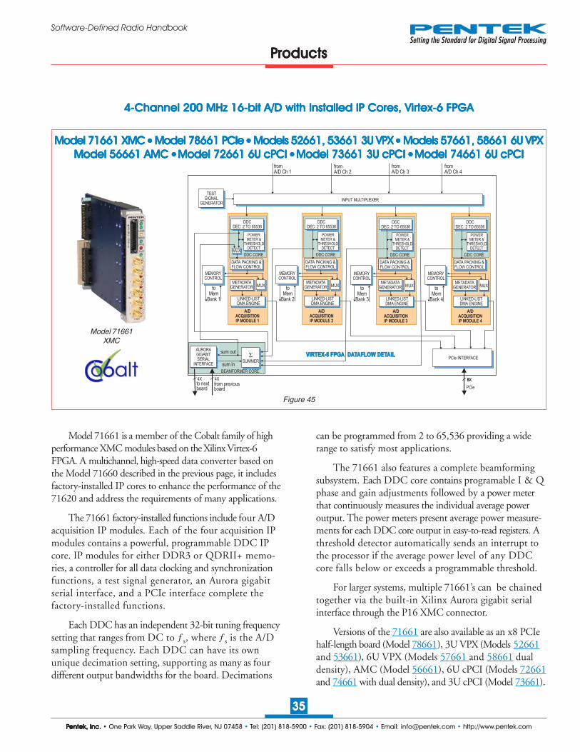
PPPPPentek, Inc.entek, Inc.entek, Inc.entek, Inc.entek, Inc. • One Park Way, Upper Saddle River, NJ 07458 • Tel: (201) 818-5900 • Fax: (201) 818-5904 • Email: [email protected] • http://www.pentek.com
3535353535
Software-Defined Radio Handbook
PPPPProductsroductsroductsroductsroducts
Figure 45
4-4-4-4-4-Channel 200 MHz 16-bit A/D with Installed IP Cores, VirChannel 200 MHz 16-bit A/D with Installed IP Cores, VirChannel 200 MHz 16-bit A/D with Installed IP Cores, VirChannel 200 MHz 16-bit A/D with Installed IP Cores, VirChannel 200 MHz 16-bit A/D with Installed IP Cores, Virtex-6 FPGAtex-6 FPGAtex-6 FPGAtex-6 FPGAtex-6 FPGA
Model 71Model 71Model 71Model 71Model 71661661661661661 XMC XMC XMC XMC XMC ●●●●● Model 78 Model 78 Model 78 Model 78 Model 78661661661661661 PCIe PCIe PCIe PCIe PCIe ●●●●● Models 52 Models 52 Models 52 Models 52 Models 52661661661661661, 53, 53, 53, 53, 53661661661661661 3U VPX 3U VPX 3U VPX 3U VPX 3U VPX ●●●●● Models 57 Models 57 Models 57 Models 57 Models 57661661661661661, 58, 58, 58, 58, 58661661661661661 6U VPX 6U VPX 6U VPX 6U VPX 6U VPXModel 56661 AMC Model 56661 AMC Model 56661 AMC Model 56661 AMC Model 56661 AMC ● ● ● ● ● Model 72661 6U cPCI Model 72661 6U cPCI Model 72661 6U cPCI Model 72661 6U cPCI Model 72661 6U cPCI ● ● ● ● ● Model 73661 3U cPCI Model 73661 3U cPCI Model 73661 3U cPCI Model 73661 3U cPCI Model 73661 3U cPCI ● ● ● ● ● Model 74661 6U cPCIModel 74661 6U cPCIModel 74661 6U cPCIModel 74661 6U cPCIModel 74661 6U cPCI
Model 71661XMC
BEAMFORMER CORE
PCIe INTERFACE
fromA/D Ch 1
fromA/D Ch 2
fromA/D Ch 3
fromA/D Ch 4
PCIe
8Xfrom previousboard
to nextboard
sum out
sum in
VIRTEX-6 FPGA DATAFLOW DETAILVIRTEX-6 FPGA DATAFLOW DETAIL
A/DACQUISITIONIP MODULE 1
A/DACQUISITIONIP MODULE 2
A/DACQUISITIONIP MODULE 3
A/DACQUISITIONIP MODULE 4
LINKED-LISTDMA ENGINE
LINKED-LISTDMA ENGINE
LINKED-LISTDMA ENGINE
LINKED-LISTDMA ENGINE
METADATAGENERATOR
METADATAGENERATOR
METADATAGENERATOR
METADATAGENERATORto
MemBank 1
MEMORYCONTROL
toMem
Bank 2
MEMORYCONTROL
toMem
Bank 3
toMem
Bank 4
MEMORYCONTROL
MEMORYCONTROL
MUX MUX MUX MUX
DATA PACKING &FLOW CONTROL
DATA PACKING &FLOW CONTROL
DATA PACKING &FLOW CONTROL
DATA PACKING &FLOW CONTROL
AURORAGIGABITSERIAL
INTERFACE
INPUT MULTIPLEXER
�
SUMMER
DDCDEC: 2 TO 65536
DDCDEC: 2 TO 65536
DDCDEC: 2 TO 65536
DDCDEC: 2 TO 65536
POWERMETER &
THRESHOLDDETECT
POWERMETER &
THRESHOLDDETECT
POWERMETER &
THRESHOLDDETECT
POWERMETER &
THRESHOLDDETECT
MUXDDC CORE DDC CORE DDC CORE DDC CORE
TESTSIGNAL
GENERATOR
DATA PACKING &FLOW CONTROL
DATA PACKING &FLOW CONTROL
8X4X 4X
Model 71661 is a member of the Cobalt family of highperformance XMC modules based on the Xilinx Virtex-6FPGA. A multichannel, high-speed data converter based onthe Model 71660 described in the previous page, it includesfactory-installed IP cores to enhance the performance of the71620 and address the requirements of many applications.
The 71661 factory-installed functions include four A/Dacquisition IP modules. Each of the four acquisition IPmodules contains a powerful, programmable DDC IPcore. IP modules for either DDR3 or QDRII+ memo-ries, a controller for all data clocking and synchronizationfunctions, a test signal generator, an Aurora gigabitserial interface, and a PCIe interface complete thefactory-installed functions.
Each DDC has an independent 32-bit tuning frequencysetting that ranges from DC to ƒs, where ƒs is the A/Dsampling frequency. Each DDC can have its ownunique decimation setting, supporting as many as fourdifferent output bandwidths for the board. Decimations
can be programmed from 2 to 65,536 providing a widerange to satisfy most applications.
The 71661 also features a complete beamformingsubsystem. Each DDC core contains programable I & Qphase and gain adjustments followed by a power meterthat continuously measures the individual average poweroutput. The power meters present average power measure-ments for each DDC core output in easy-to-read registers. Athreshold detector automatically sends an interrupt tothe processor if the average power level of any DDCcore falls below or exceeds a programmable threshold.
For larger systems, multiple 71661’s can be chainedtogether via the built-in Xilinx Aurora gigabit serialinterface through the P16 XMC connector.
Versions of the 71661 are also available as an x8 PCIehalf-length board (Model 78661), 3U VPX (Models 52661and 53661), 6U VPX (Models 57661 and 58661 dualdensity), AMC (Model 56661), 6U cPCI (Models 72661and 74661 with dual density), and 3U cPCI (Model 73661).
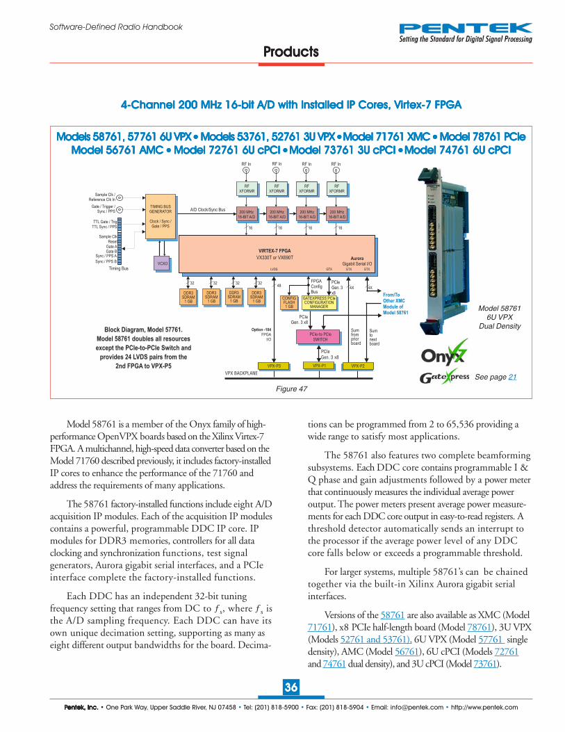
PPPPPentek, Inc.entek, Inc.entek, Inc.entek, Inc.entek, Inc. • One Park Way, Upper Saddle River, NJ 07458 • Tel: (201) 818-5900 • Fax: (201) 818-5904 • Email: [email protected] • http://www.pentek.com
3636363636
Software-Defined Radio Handbook
PPPPProductsroductsroductsroductsroducts
4-4-4-4-4-Channel 200 MHz 16-bit A/D with Installed IP Cores, VirChannel 200 MHz 16-bit A/D with Installed IP Cores, VirChannel 200 MHz 16-bit A/D with Installed IP Cores, VirChannel 200 MHz 16-bit A/D with Installed IP Cores, VirChannel 200 MHz 16-bit A/D with Installed IP Cores, Virtex-7 FPGAtex-7 FPGAtex-7 FPGAtex-7 FPGAtex-7 FPGA
Models 5Models 5Models 5Models 5Models 588888761, 5761, 5761, 5761, 5761, 577777761 6U VPX 761 6U VPX 761 6U VPX 761 6U VPX 761 6U VPX ●●●●● Models 53761, 52761 3U VPX Models 53761, 52761 3U VPX Models 53761, 52761 3U VPX Models 53761, 52761 3U VPX Models 53761, 52761 3U VPX ● ● ● ● ● Model 71761 XMC Model 71761 XMC Model 71761 XMC Model 71761 XMC Model 71761 XMC ●●●●● Model 78761 PCIe Model 78761 PCIe Model 78761 PCIe Model 78761 PCIe Model 78761 PCIeModel 56761 AMC Model 56761 AMC Model 56761 AMC Model 56761 AMC Model 56761 AMC ●●●●● Model 72761 6U cPCI Model 72761 6U cPCI Model 72761 6U cPCI Model 72761 6U cPCI Model 72761 6U cPCI ● ● ● ● ● Model 73761 3U cPCI Model 73761 3U cPCI Model 73761 3U cPCI Model 73761 3U cPCI Model 73761 3U cPCI ● ● ● ● ● Model 74761 6U cPCIModel 74761 6U cPCIModel 74761 6U cPCIModel 74761 6U cPCIModel 74761 6U cPCI
Model 587616U VPX
Dual Density
Figure 47
Model 58761 is a member of the Onyx family of high-performance OpenVPX boards based on the Xilinx Virtex-7FPGA. A multichannel, high-speed data converter based on theModel 71760 described previously, it includes factory-installedIP cores to enhance the performance of the 71760 andaddress the requirements of many applications.
The 58761 factory-installed functions include eight A/Dacquisition IP modules. Each of the acquisition IP modulescontains a powerful, programmable DDC IP core. IPmodules for DDR3 memories, controllers for all dataclocking and synchronization functions, test signalgenerators, Aurora gigabit serial interfaces, and a PCIeinterface complete the factory-installed functions.
Each DDC has an independent 32-bit tuningfrequency setting that ranges from DC to ƒs, where ƒs isthe A/D sampling frequency. Each DDC can have itsown unique decimation setting, supporting as many aseight different output bandwidths for the board. Decima-
tions can be programmed from 2 to 65,536 providing awide range to satisfy most applications.
The 58761 also features two complete beamformingsubsystems. Each DDC core contains programmable I &Q phase and gain adjustments followed by a power meterthat continuously measures the individual average poweroutput. The power meters present average power measure-ments for each DDC core output in easy-to-read registers. Athreshold detector automatically sends an interrupt tothe processor if the average power level of any DDCcore falls below or exceeds a programmable threshold.
For larger systems, multiple 58761’s can be chainedtogether via the built-in Xilinx Aurora gigabit serialinterfaces.
Versions of the 58761 are also available as XMC (Model71761), x8 PCIe half-length board (Model 78761), 3U VPX(Models 52761 and 53761), 6U VPX (Model 57761 singledensity), AMC (Model 56761), 6U cPCI (Models 72761and 74761 dual density), and 3U cPCI (Model 73761).
See page 21
LVDS
48
FPGAI/O
Option -104
VPX BACKPLANE
VPX-P3
VIRTEX-7 FPGA
VX330T or VX690T
DDR3SDRAM
1 GB
DDR3SDRAM
1 GB
DDR3SDRAM
1 GB
DDR3SDRAM
1 GB
32 32 32 32
GTXGTXGTX
PCIeGen. 3 x8
4X4X
PCIeGen. 3 x8
CONFIGFLASH1 GB
PCIeGen. 3x8
FPGAConfigBus
GATEXPRESS PCIeCONFIGURATION
MANAGER
VPX-P2VPX-P1
PCIe-to PCIeSWITCH
From/ToOther XMCModule ofModel 58761
AuroraGigabit Serial I/O
Block Diagram, Model 57761.
Model 58761 doubles all resources
except the PCIe-to-PCIe Switch and
provides 24 LVDS pairs from the
2nd FPGA to VPX-P5
Sumtonextboard
Sumfrompriorboard
TIMING BUSGENERATOR
Clock / Sync /Gate / PPS
200 MHz16-BIT A/D
RF In
RFXFORMR
RF In
RFXFORMR
TTL Gate / TrigTTL Sync / PPS
Sample ClkReset
Gate AGate B
Sync / PPS A
Sync / PPS B
Timing Bus
200 MHz16-BIT A/D
Sample Clk /Reference Clk In
A/D Clock/Sync Bus
1616
RF In
RFXFORMR
200 MHz16-BIT A/D
16
RF In
RFXFORMR
200 MHz16-BIT A/D
16
Gate / Trigger /Sync / PPS
VCXO

PPPPPentek, Inc.entek, Inc.entek, Inc.entek, Inc.entek, Inc. • One Park Way, Upper Saddle River, NJ 07458 • Tel: (201) 818-5900 • Fax: (201) 818-5904 • Email: [email protected] • http://www.pentek.com
3737373737
Software-Defined Radio Handbook
fromA/D Ch 1
fromA/D Ch 2
fromA/D Ch 3
fromA/D Ch 4
VIRTEX-6 FPGA DATAFLOW DETAILVIRTEX-6 FPGA DATAFLOW DETAIL
A/DACQUISITIONIP MODULE 1
A/DACQUISITIONIP MODULE 2
A/DACQUISITIONIP MODULE 3
A/DACQUISITIONIP MODULE 4
LINKED-LISTDMA ENGINE
LINKED-LISTDMA ENGINE
METADATAGENERATOR
METADATAGENERATOR
METADATAGENERATOR
METADATAGENERATORto
MemBank 1
MEMORYCONTROL
toMem
Bank 2
MEMORYCONTROL
toMem
Bank 3
toMem
Bank 4
MEMORYCONTROL
MEMORYCONTROL
MUX MUX MUX MUX
DATA PACKING &FLOW CONTROL
DATA PACKING &FLOW CONTROL
DATA PACKING &FLOW CONTROL
DATA PACKING &FLOW CONTROL
INPUT MULTIPLEXER
TESTSIGNAL
GENERATOR
DATA PACKING &FLOW CONTROL
DATA PACKING &FLOW CONTROL
DDCCORE
DIGITALDOWN-
CONVERTER
BANK 1: CH 1-8DEC: 16 TO 8192
.
DDCCORE
DIGITALDOWN-
CONVERTER
BANK 2: CH 9-16DEC: 16 TO 8192
.
DDCCORE
DIGITALDOWN-
CONVERTER
BANK 3: CH 17-24DEC: 16 TO 8192
.
DDCCORE
DIGITALDOWN-
CONVERTER
BANK 4: CH 18-32DEC: 16 TO 8192
.
MemoryBank 4
PCIe INTERFACE
PCIe8X
LINKED-LISTDMA ENGINE
LINKED-LISTDMA ENGINE
GigabitSerial I/O
FPGAGPIO
(supports user installed IP)
4X 4X 4032MemoryBank 3
32MemoryBank 2
32MemoryBank 1
32
Figure 48
PPPPProductsroductsroductsroductsroducts
4-4-4-4-4-Channel 200 MHz 16-bit A/D with Installed IP Cores, VirChannel 200 MHz 16-bit A/D with Installed IP Cores, VirChannel 200 MHz 16-bit A/D with Installed IP Cores, VirChannel 200 MHz 16-bit A/D with Installed IP Cores, VirChannel 200 MHz 16-bit A/D with Installed IP Cores, Virtex-6 FPGAtex-6 FPGAtex-6 FPGAtex-6 FPGAtex-6 FPGA
Model 786Model 786Model 786Model 786Model 7866262626262 PCIe PCIe PCIe PCIe PCIe ● ● ● ● ● Model 716Model 716Model 716Model 716Model 7166262626262 XMC XMC XMC XMC XMC ●●●●● Model 526 Model 526 Model 526 Model 526 Model 5266262626262, 536, 536, 536, 536, 5366262626262 3U VPX 3U VPX 3U VPX 3U VPX 3U VPX ● ● ● ● ● Model 57Model 57Model 57Model 57Model 57662662662662662, 586, 586, 586, 586, 5866262626262 6U VPX 6U VPX 6U VPX 6U VPX 6U VPXModel 56662 AMC Model 56662 AMC Model 56662 AMC Model 56662 AMC Model 56662 AMC ●●●●● Model 72662 6U cPCI Model 72662 6U cPCI Model 72662 6U cPCI Model 72662 6U cPCI Model 72662 6U cPCI ● ● ● ● ● Model 73662 3U cPCI Model 73662 3U cPCI Model 73662 3U cPCI Model 73662 3U cPCI Model 73662 3U cPCI ● ● ● ● ● Model 74662 6U cPCIModel 74662 6U cPCIModel 74662 6U cPCIModel 74662 6U cPCIModel 74662 6U cPCI
Model 78662 is a member of the Cobalt family ofhigh performance PCIe boards based on the Xilinx Virtex-6FPGA. Based on the Model 71660 presented previously,this four-channel, high-speed data converter withprogrammable DDCs is suitable for connection to HF orIF ports of a communications or radar system.
The 78662 factory-installed functions include four A/Dacquisition IP modules. Each of the four acquisition IPmodules contains a powerful, programmable 8-channelDDC IP core. IP modules for either DDR3 or QDRII+memories, a controller for all data clocking and synchroni-zation functions, a test signal generator, voltage andtemperature monitoring, and a PCIe interface complete thefactory-installed functions.
Each of the 32 DDC channels has an independent32-bit tuning frequency setting that ranges from DC toƒs, where ƒs is the A/D sampling frequency. All of the8 channels within a bank share a common decimationsetting ranging from 16 to 8192. Each 8-channel bank
can have its own unique decimation setting supportinga different bandwidth associated with each of the fouracquisition modules.
The decimating filter for each DDC bank accepts aunique set of user-supplied 18-bit coefficients. The 80%default filters deliver an output bandwidth of 0.8*ƒs/N,where N is the decimation setting. The rejection ofadjacent-band components is better than 100 dB.
Each DDC delivers a complex output stream consistingof 24-bit I + 24-bit Q samples at a rate of ƒs/N. Anynumber of channels can be enabled within each bank,selectable from 0 to 8. Multiple 78662’s can be drivenfrom the LVPECL bus master, supporting synchronoussampling and sync functions across all connected boards.
Versions of the 78662 are also available as an XMCmodule (Model 71662), 3U VPX (Models 52662 and53662), 6U VPX (Models 57662 and 58662 with dualdensity), AMC (Model 56662), 6U cPCI (Models 72662and 74662 with dual density), and 3U cPCI (Model 73662).
Model 78662x8 PCIe
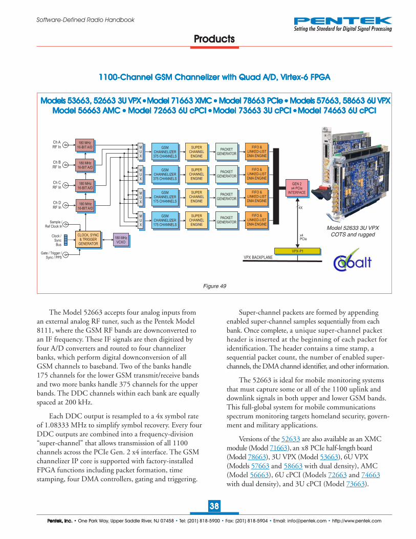
PPPPPentek, Inc.entek, Inc.entek, Inc.entek, Inc.entek, Inc. • One Park Way, Upper Saddle River, NJ 07458 • Tel: (201) 818-5900 • Fax: (201) 818-5904 • Email: [email protected] • http://www.pentek.com
3838383838
Software-Defined Radio Handbook
SUPERCHANNELENGINE
PACKETGENERATOR
FIFO &LINKED-LISTDMA ENGINE
GEN 2x4 PCIe
INTERFACE
SUPERCHANNELENGINE
SUPERCHANNELENGINE
SUPERCHANNELENGINE
PACKETGENERATOR
PACKETGENERATOR
PACKETGENERATOR
FIFO &LINKED-LISTDMA ENGINE
FIFO &LINKED-LISTDMA ENGINE
FIFO &LINKED-LISTDMA ENGINE
Sample /Ref Clock In
MUX
180 MHz16-BIT A/D
Ch ARF In GSM
CHANNELIZER375 CHANNELS
MUX
MUX
MUX
Ch BRF In
Ch CRF In
Ch DRF In
180 MHzVCXO
CLOCK, SYNC& TRIGGER
GENERATOR
Clock /SyncBus
GSMCHANNELIZER375 CHANNELS
GSMCHANNELIZER175 CHANNELS
GSMCHANNELIZER175 CHANNELS
180 MHz16-BIT A/D
180 MHz16-BIT A/D
180 MHz16-BIT A/D
Gate / Trigger /Sync / PPS VPX BACKPLANE
VPX-P1
4X
x4PCIe
Figure 49
PPPPProductsroductsroductsroductsroducts
1100-1100-1100-1100-1100-Channel GSM Channelizer with Quad A/D, VirChannel GSM Channelizer with Quad A/D, VirChannel GSM Channelizer with Quad A/D, VirChannel GSM Channelizer with Quad A/D, VirChannel GSM Channelizer with Quad A/D, Virtex-6 FPGAtex-6 FPGAtex-6 FPGAtex-6 FPGAtex-6 FPGA
Models 53Models 53Models 53Models 53Models 53663663663663663, 52, 52, 52, 52, 52663663663663663 3U VPX 3U VPX 3U VPX 3U VPX 3U VPX ● ● ● ● ● Model 71Model 71Model 71Model 71Model 71663663663663663 XMC XMC XMC XMC XMC ●●●●● Model 78 Model 78 Model 78 Model 78 Model 78663663663663663 PCIe PCIe PCIe PCIe PCIe ●●●●● Models 57 Models 57 Models 57 Models 57 Models 57663663663663663, 58, 58, 58, 58, 58663663663663663 6U VPX 6U VPX 6U VPX 6U VPX 6U VPXModel 56663 AMC Model 56663 AMC Model 56663 AMC Model 56663 AMC Model 56663 AMC ●●●●● Model 72663 6U cPCI Model 72663 6U cPCI Model 72663 6U cPCI Model 72663 6U cPCI Model 72663 6U cPCI ● ● ● ● ● Model 73663 3U cPCI Model 73663 3U cPCI Model 73663 3U cPCI Model 73663 3U cPCI Model 73663 3U cPCI ● ● ● ● ● Model 74663 6U cPCIModel 74663 6U cPCIModel 74663 6U cPCIModel 74663 6U cPCIModel 74663 6U cPCI
Model 52633 3U VPXCOTS and rugged
The Model 52663 accepts four analog inputs froman external analog RF tuner, such as the Pentek Model8111, where the GSM RF bands are downconverted toan IF frequency. These IF signals are then digitized byfour A/D converters and routed to four channelizerbanks, which perform digital downconversion of allGSM channels to baseband. Two of the banks handle175 channels for the lower GSM transmit/receive bandsand two more banks handle 375 channels for the upperbands. The DDC channels within each bank are equallyspaced at 200 kHz.
Each DDC output is resampled to a 4x symbol rateof 1.08333 MHz to simplify symbol recovery. Every fourDDC outputs are combined into a frequency-division“super-channel” that allows transmission of all 1100channels across the PCIe Gen. 2 x4 interface. The GSMchannelizer IP core is supported with factory-installedFPGA functions including packet formation, timestamping, four DMA controllers, gating and triggering.
Super-channel packets are formed by appendingenabled super-channel samples sequentially from eachbank. Once complete, a unique super-channel packetheader is inserted at the beginning of each packet foridentification. The header contains a time stamp, asequential packet count, the number of enabled super-channels, the DMA channel identifier, and other information.
The 52663 is ideal for mobile monitoring systemsthat must capture some or all of the 1100 uplink anddownlink signals in both upper and lower GSM bands.This full-global system for mobile communicationsspectrum monitoring targets homeland security, govern-ment and military applications.
Versions of the 52633 are also available as an XMCmodule (Model 71663), an x8 PCIe half-length board(Model 78663), 3U VPX (Model 53663), 6U VPX(Models 57663 and 58663 with dual density), AMC(Model 56663), 6U cPCI (Models 72663 and 74663with dual density), and 3U cPCI (Model 73663).

PPPPPentek, Inc.entek, Inc.entek, Inc.entek, Inc.entek, Inc. • One Park Way, Upper Saddle River, NJ 07458 • Tel: (201) 818-5900 • Fax: (201) 818-5904 • Email: [email protected] • http://www.pentek.com
3939393939
Software-Defined Radio Handbook
Figure 50
4-4-4-4-4-Channel 1.25 GHz D/A with DUC, VirChannel 1.25 GHz D/A with DUC, VirChannel 1.25 GHz D/A with DUC, VirChannel 1.25 GHz D/A with DUC, VirChannel 1.25 GHz D/A with DUC, Virtex-6 FPGAtex-6 FPGAtex-6 FPGAtex-6 FPGAtex-6 FPGA
Models 5Models 5Models 5Models 5Models 576707670767076707670, 5, 5, 5, 5, 586708670867086708670 6U VPX 6U VPX 6U VPX 6U VPX 6U VPX ●●●●● Models 53 Models 53 Models 53 Models 53 Models 53670670670670670, 52, 52, 52, 52, 52670670670670670 3U VPX 3U VPX 3U VPX 3U VPX 3U VPX ● ● ● ● ● Model 71Model 71Model 71Model 71Model 71670670670670670 XMC XMC XMC XMC XMC ●●●●● Model 78 Model 78 Model 78 Model 78 Model 78670670670670670 PCIe PCIe PCIe PCIe PCIeModel 56670 AMC Model 56670 AMC Model 56670 AMC Model 56670 AMC Model 56670 AMC ●●●●● Model 72670 6U cPCI Model 72670 6U cPCI Model 72670 6U cPCI Model 72670 6U cPCI Model 72670 6U cPCI ● ● ● ● ● Model 73670 3U cPCI Model 73670 3U cPCI Model 73670 3U cPCI Model 73670 3U cPCI Model 73670 3U cPCI ● ● ● ● ● Model 74670 6U cPCIModel 74670 6U cPCIModel 74670 6U cPCIModel 74670 6U cPCIModel 74670 6U cPCI
Model 576706U VPX
Single Density
Model 57670 is a member of the Cobalt family ofhigh performance 6U OpenVPX boards based on theXilinx Virtex-6 FPGA. This 4-channel, high-speed dataconverter is suitable for connection to transmit HF or IFports of a communications or radar system. Its built-indata playback features offer an ideal turnkey solutionfor demanding transmit applications. It includes fourD/As, four digital upconverters and four banks ofmemory. In addition to supporting PCI Express Gen. 2 asa native interface, the Model 57670 includes a front panelgeneral-purpose connector for application-specific I/O.
The Pentek Cobalt Architecture features a Virtex-6FPGA. All of the board’s data and control paths areaccessible by the FPGA, enabling factory-installed functionsincluding data multiplexing, channel selection, datapacking, gating, triggering and memory control. TheCobalt Architecture organizes the FPGA as a containerfor data processing applications where each functionexists as an intellectual property (IP) module.
Each member of the Cobalt family is delivered withfactory-installed applications ideally matched to the board’sanalog interfaces. The Model 57670 factory-installedfunctions include a sophisticated D/A WaveformPlayback IP module. Four linked-list controllers supportwaveform generation to the four D/As from tables storedin either on-board memory or off-board host memory.
IP modules for DDR3 SDRAM memories, acontroller for all data clocking and synchronizationfunctions, a test signal generator, and a PCIe interfacecomplete the factory-installed functions and enable the57670 to operate as a turnkey solution without the need todevelop FPGA IP.
Versions of the 57670 are also available as XMC(Model 71670), x8 PCIe (Model 78670), 3U VPX (Models52670 and 53670), 6U VPX (Model 58670 dual density),AMC (Model 56670), 6U cPCI (Models 72670 and74670 dual density), and 3U cPCI (Model 73670).
PPPPProductsroductsroductsroductsroducts
VIRTEX-6 FPGA
LX130T, LX240T or SX315T
16
ConfigFLASH64 MB
LVDS GTX
40 8X
FPGAI/O
Option -104
VPX BACKPLANE
VPX-P3
GTXGTX
PCIeGen. 2 x8
4X 4X
VPX-P2VPX-P1
Option -105Gigabit Serial I/O
TIMING BUSGENERATOR
Clock / Sync /Gate / PPS
VCXO
Sample Clk /Reference Clk In
Clock/SyncBus A
RFXFORMR
16-BIT D/A1.25 GHz
DIGITALUPCONVERTER
RF Out
RFXFORMR
RFXFORMR
1.25 GHz16-BIT D/A
DIGITALUPCONVERTER
RF Out
RFXFORMR
RFXFORMR
16-BIT D/A1.25 GHz
DIGITALUPCONVERTER
RF Out
RFXFORMR
RFXFORMR
1.25 GHz16-BIT D/A
DIGITALUPCONVERTER
RF Out
RFXFORMR
16 16
Gate InSync In
�Sync Bus A
Gate InSync In
�Sync Bus B
Trigger In
Clock/SyncBus B
3232
DDR3SDRAM512 MB
DDR3SDRAM512 MB
3232
DDR3SDRAM512 MB
DDR3SDRAM512 MB
Memory Banks 1 & 2 Memory Banks 3 & 4

PPPPPentek, Inc.entek, Inc.entek, Inc.entek, Inc.entek, Inc. • One Park Way, Upper Saddle River, NJ 07458 • Tel: (201) 818-5900 • Fax: (201) 818-5904 • Email: [email protected] • http://www.pentek.com
4040404040
Software-Defined Radio Handbook
Figure 51
PPPPProductsroductsroductsroductsroducts
4-4-4-4-4-Channel 1.25 GHz D/A with DUC, Extended InterpolationChannel 1.25 GHz D/A with DUC, Extended InterpolationChannel 1.25 GHz D/A with DUC, Extended InterpolationChannel 1.25 GHz D/A with DUC, Extended InterpolationChannel 1.25 GHz D/A with DUC, Extended Interpolation, Vir, Vir, Vir, Vir, Virtex-6 FPGAtex-6 FPGAtex-6 FPGAtex-6 FPGAtex-6 FPGA
Model 71Model 71Model 71Model 71Model 71671671671671671 XMC XMC XMC XMC XMC ●●●●● Model 78 Model 78 Model 78 Model 78 Model 78671671671671671 PCIe PCIe PCIe PCIe PCIe ●●●●● Models 52 Models 52 Models 52 Models 52 Models 52671671671671671, 53, 53, 53, 53, 53671671671671671 3U VPX 3U VPX 3U VPX 3U VPX 3U VPX ●●●●● Models 57 Models 57 Models 57 Models 57 Models 57671671671671671, 58, 58, 58, 58, 58671671671671671 6U VPX 6U VPX 6U VPX 6U VPX 6U VPXModel 56671 AMC Model 56671 AMC Model 56671 AMC Model 56671 AMC Model 56671 AMC ● ● ● ● ● Model 72671 6U cPCI Model 72671 6U cPCI Model 72671 6U cPCI Model 72671 6U cPCI Model 72671 6U cPCI ● ● ● ● ● Model 73671 3U cPCI Model 73671 3U cPCI Model 73671 3U cPCI Model 73671 3U cPCI Model 73671 3U cPCI ● ● ● ● ● Model 74671 6U cPCIModel 74671 6U cPCIModel 74671 6U cPCIModel 74671 6U cPCIModel 74671 6U cPCI
D/AWAVEFORMPLAYBACK
IP MODULE 1
toD/A Ch 1 & 2
GigabitSerial I/OPCIe
FPGAGPIO
(supports user installed IP)
MemoryBank 1
MemoryBank 2
MemoryBank 3
MemoryBank 4
VIRTEX-6 FPGA DATAFLOW DETAILVIRTEX-6 FPGA DATAFLOW DETAIL
DATAUNPACKING
& FLOWCONTROL
MUX
LINKED-LISTDMA ENGINE
toMem
Bank 1
MEMORYCONTROL
8X 4X 4X 40
D/AWAVEFORMPLAYBACK
IP MODULE 2
DATAUNPACKING
& FLOWCONTROL
MUX
LINKED-LISTDMA ENGINE
toMem
Bank 2
MEMORYCONTROL
D/AWAVEFORMPLAYBACK
IP MODULE 3
DATAUNPACKING
& FLOWCONTROL
MUX
LINKED-LISTDMA ENGINE
toMem
Bank 3
MEMORYCONTROL
D/AWAVEFORMPLAYBACK
IP MODULE 4
DATAUNPACKING
& FLOWCONTROL
MUX
LINKED-LISTDMA ENGINE
toMem
Bank 4
MEMORYCONTROL
TESTSIGNAL
GENERATOR
PCIe INTERFACE
DATAINTERLEAVER
16toD/A Ch 3 & 4
DATAINTERLEAVER
16
INTERPOLATOR2 TO 65536
IP CORE
INTERPOLATOR2 TO 65536
IP CORE
INTERPOLATOR2 TO 65536
IP CORE
INTERPOLATOR2 TO 65536
IP CORE
Model 71671XMC
Model 71671 is a member of the Cobalt family of highperformance XMC modules based on the Xilinx Virtex-6FPGA. A multichannel, high-speed data converter based onthe Model 71670 described previously, it includes factory-installed IP cores to enhance the performance of the 71670and address the requirements of many applications.
The Model 56671 factory-installed functionsinclude a sophisticated D/A Waveform Playback IPmodule. Four linked-list controllers support waveformgeneration to the four D/As from tables stored in eitheron-board memory or off-board host memory.
Two Texas Instruments DAC3484s provide four DUC(digital upconverter) and D/A channels. Each channelaccepts a baseband real or complex data stream from theFPGA and provides that input to the upconvert, interpo-late and D/A stage.
When operating as a DUC, it interpolates and trans-lates real or complex baseband input signals to a user
selectable IF center frequency. It delivers real or quadra-ture (I+Q) analog outputs to a 16-bit D/A converter.
If translation is disabled, each D/A acts as aninterpolating 16-bit D/A with output sampling rates upto 1.25 GHz. In both modes, the D/A provides interpolationfactors of 2x, 4x, 8x and 16x.
In addition to the DAC3484, the 71671 features anFPGA-based interpolation engine which adds twoadditonal interpolation stages programmable from 2x to256x. The combined interpolation results in a rangefrom 2x to 1,048,576x for each D/A channel and is idealfor matching the digital downconversion and datareduction used on the receiving channels of manycommunications systems.
Versions of the 71761 are also available as an x8 PCIe half-length board (Model 78671), 3U VPX (Models 52671 and53671), 6U VPX (Models 57671 and 58671 with dualdensity), AMC (Model 56671), 6U cPCI (Models 72671and 74671 with dual density), and 3U cPCI (Model 73671).

PPPPPentek, Inc.entek, Inc.entek, Inc.entek, Inc.entek, Inc. • One Park Way, Upper Saddle River, NJ 07458 • Tel: (201) 818-5900 • Fax: (201) 818-5904 • Email: [email protected] • http://www.pentek.com
4141414141
Software-Defined Radio Handbook
Figure 52
PPPPProductsroductsroductsroductsroducts
4-4-4-4-4-Channel 1.25 GHz D/A with DUC, Extended InterpolationChannel 1.25 GHz D/A with DUC, Extended InterpolationChannel 1.25 GHz D/A with DUC, Extended InterpolationChannel 1.25 GHz D/A with DUC, Extended InterpolationChannel 1.25 GHz D/A with DUC, Extended Interpolation, Vir, Vir, Vir, Vir, Virtex-7 FPGAtex-7 FPGAtex-7 FPGAtex-7 FPGAtex-7 FPGA
Model 71771 XMC Model 71771 XMC Model 71771 XMC Model 71771 XMC Model 71771 XMC ●●●●● Model 78771 PCIe Model 78771 PCIe Model 78771 PCIe Model 78771 PCIe Model 78771 PCIe ●●●●● Model 52771 3U VPX Model 52771 3U VPX Model 52771 3U VPX Model 52771 3U VPX Model 52771 3U VPX ● ● ● ● ● Model 53771 3U VPXModel 53771 3U VPXModel 53771 3U VPXModel 53771 3U VPXModel 53771 3U VPX Model 56771 AMC Model 56771 AMC Model 56771 AMC Model 56771 AMC Model 56771 AMC ● ● ● ● ● Model 72771 6U cPCI Model 72771 6U cPCI Model 72771 6U cPCI Model 72771 6U cPCI Model 72771 6U cPCI ● ● ● ● ● Model 73771 3U cPCI Model 73771 3U cPCI Model 73771 3U cPCI Model 73771 3U cPCI Model 73771 3U cPCI ● ● ● ● ● Model 74771 6U cPCIIModel 74771 6U cPCIIModel 74771 6U cPCIIModel 74771 6U cPCIIModel 74771 6U cPCII
Model 71771XMC
TIMING BUSGENERATOR
Clock / Sync /Gate / PPS
VCXO
Sample Clk /Reference Clk In
Clock/SyncBus A
RFXFORMR
16-BIT D/A1.25 GHz
DIGITALUPCONVERTER
RF Out
RFXFORMR
RFXFORMR
1.25 GHz16-BIT D/A
DIGITALUPCONVERTER
RF Out
RFXFORMR
RFXFORMR
16-BIT D/A1.25 GHz
DIGITALUPCONVERTER
RF Out
RFXFORMR
RFXFORMR
1.25 GHz16-BIT D/A
DIGITALUPCONVERTER
RF Out
RFXFORMR
16 16
Gate InSync In
�Sync Bus A
Gate InSync In
�Sync Bus B
Trigger In
Clock/SyncBus B
VIRTEX-7 FPGA
VX330T or VX690T
GigabitSerial I/O(option 105)
GTXGTX LVDSGTX
FPGAGPIO(option 104)
PCIeGen. 3 x8
P14PMC
P16XMC
P15XMC
4X4XCONFIGFLASH1 GB
DDR3SDRAM
1 GB
DDR3SDRAM
1 GB
DDR3SDRAM
1 GB
DDR3SDRAM
1 GB
48 32 32 32 32PCIeGen. 3 x8
FPGAConfigBus
GATEXPRESS PCIeCONFIGURATION
MANAGER
Model 71771 is a member of the Onyx family ofhigh performance XMC modules based on the XilinxVirtex-7 FPGA. This 4-channel, high-speed dataconverter is suitable for connection to transmit HF or IFports of a communications or radar system. Its built-indata playback features offer an ideal turnkey solutionfor demanding transmit applications.
It includes four digital upconverters, four D/Aswith a wide range of programmable interpolation factors,and four banks of memory. In addition to supporting PCIExpress Gen. 3 as a native interface, the Model 71771includes optional general-purpose and gigabit serialconnectors for application-specific I/O.
The Pentek Onyx architecture features a Virtex-7FPGA. All of the board’s data and control paths areaccessible by the FPGA, enabling factory-installedfunctions including data multiplexing, channel selection,data packing, gating, triggering and memory control.
The Model 71771 factory-installed functionsinclude a sophisticated D/A Waveform Playback IPmodule to support waveform generation to the fourD/As from tables stored in on-board or off-board hostmemory.
Two Texas Instruments DAC3484s provide four DUCand D/A channels with interpolation factors of 2x, 4x, 8x and16x. In addition to the DAC3484, the 71771 features anFPGA-based interpolation engine. The combined totalinterpolation results in a range from 2x to 1,048,576x foreach D/A channel and is ideal for matching the digitaldownconversion and data reduction used on the receivingchannels of many communications systems. See the blockdiagram of the 71671 on the previous page for more detail.
Versions of the 71771 are also available as an x8 PCIe half-length board (Model 78771), 3U VPX (Models 52771 and53771), 6U VPX (Models 57771 and 58771 with dualdensity), AMC (Model 56771), 6U cPCI (Models 72771and 74771 with dual density), and 3U cPCI (Model 73771).
See page 21

PPPPPentek, Inc.entek, Inc.entek, Inc.entek, Inc.entek, Inc. • One Park Way, Upper Saddle River, NJ 07458 • Tel: (201) 818-5900 • Fax: (201) 818-5904 • Email: [email protected] • http://www.pentek.com
4242424242
Software-Defined Radio Handbook
LLLLL-Band RF T-Band RF T-Band RF T-Band RF T-Band RF Tuner with 2-uner with 2-uner with 2-uner with 2-uner with 2-Channel 200 MHz A/D and VirChannel 200 MHz A/D and VirChannel 200 MHz A/D and VirChannel 200 MHz A/D and VirChannel 200 MHz A/D and Virtex-6 FPGAtex-6 FPGAtex-6 FPGAtex-6 FPGAtex-6 FPGA
Models 53Models 53Models 53Models 53Models 53690690690690690, 52, 52, 52, 52, 52690690690690690 3U VPX 3U VPX 3U VPX 3U VPX 3U VPX ● ● ● ● ● Model 71Model 71Model 71Model 71Model 71690690690690690 XMC XMC XMC XMC XMC ●●●●● Model 78 Model 78 Model 78 Model 78 Model 78690690690690690 PCIe PCIe PCIe PCIe PCIe ●●●●● Models 57 Models 57 Models 57 Models 57 Models 57690690690690690, 58, 58, 58, 58, 58690690690690690 6U VPX 6U VPX 6U VPX 6U VPX 6U VPXModel 56690 AMC Model 56690 AMC Model 56690 AMC Model 56690 AMC Model 56690 AMC ●●●●● Model 72690 6U cPCI Model 72690 6U cPCI Model 72690 6U cPCI Model 72690 6U cPCI Model 72690 6U cPCI ● ● ● ● ● Model 73690 3U cPCI Model 73690 3U cPCI Model 73690 3U cPCI Model 73690 3U cPCI Model 73690 3U cPCI ● ● ● ● ● Model 74690 6U cPCIModel 74690 6U cPCIModel 74690 6U cPCIModel 74690 6U cPCIModel 74690 6U cPCI
Figure 53
PPPPProductsroductsroductsroductsroducts
Model 53690 3U VPXCOTS and rugged
VCXO
16
QDRII+SRAM8 MB
TTL Gate / TrigTTL Sync / PPS
Sample ClkRef In
Gate AGate B
Sync / PPS A
Sync / PPS B
Timing Bus
Sample Clk /Reference Clk In
A/D Clock/Sync
16 16
ConfigFLASH64 MB
16
QDRII+SRAM8 MB
16
DDR3SDRAM512 MB
DDR3SDRAM512 MB
QDRII+ option 150
16
QDRII+SRAM8 MB
1616
QDRII+SRAM8 MB
16
DDR3SDRAM512 MB
DDR3SDRAM512 MB
Memory Banks 1 & 2 Memory Banks 3 & 4
DDR3 option 155
QDRII+ option 160
DDR3 option 165
Trigger 1
200 MHz16-BIT A/D
200 MHz16-BIT A/D
1616
MAX2112
I Q
RefIn
RFIn
RefOut
12-BITD/A
2
I C2
GC
Control
Trigger 2
TIMINGGENERATOR
Clock / Sync /Gate / PPS
Ref
40
FPGAI/O
Option -104
VPX BACKPLANE
VPX-P2
GTXGTXGTXLVDS
Gigabit Serial I/O
4XGbitSerial
4XGbitSerial
4XGbitSerial
4XGbitSerial
CROSSBARSWITCH
VPX-P1
4X8X 4X
x8PCIe
Option -105
VIRTEX-6 FPGA
LX130T, LX240T or SX315T
Model 53690 is a member of the Cobalt family ofhigh performance 3U VPX boards based on the XilinxVirtex-6 FPGA. A 2-channel high-speed data converter, itis suitable for connection directly to the RF port of acommunications or radar system. Its built-in data capturefeatures offer an ideal turnkey solution. The Model 53690includes an L-Band RF tuner, two 200 MHz, 16-bitA/Ds and four banks of memory. It features built-insupport for PCI Express over the 3U VPX backplane.
The Pentek Cobalt architecture features a Virtex-6FPGA. All of the board’s data and control paths are acces-sible by the FPGA, enabling factory-installed functionsincluding data multiplexing, channel selection, data packing,gating, triggering and memory control. The Cobalt architec-ture organizes the FPGA as a container for data processingapplications where each function exists as an intellec-tual property (IP) module.
Each member of the Cobalt family is delivered withfactory-installed applications ideally matched to the
board’s analog interfaces. The 53690 factory-installedfunctions include two A/D acquisition IP modules. IPmodules for either DDR3 or QDRII+ memories, acontroller for all data clocking and synchronizationfunctions, a test signal generator, and a PCIe interfacecomplete the factory-installed functions.
A front panel connector accepts L-Band signalsbetween 925 MHz and 2175 MHz from an antenna LNB.A Maxim MAX2112 tuner directly converts these signals tobaseband using a broadband I/Q downconverter. The deviceincludes an RF variable-gain LNA (low-noise amplifier), aPLL synthesized local oscillator, quadrature (I + Q) down-converting mixers, baseband lowpass filters and variable-gain baseband amplifiers.
Versions of the 53690 are also available as an XMC(Model 71690), an x8 PCI board (Model 78690), 3U VPX(Model 52690), 6U VPX (Models 57690 and 58690 dualdensity), AMC (Model 56690), 6U cPCI (Models 72690and 74690 dual density), and 3U cPCI (Model 73690).

PPPPPentek, Inc.entek, Inc.entek, Inc.entek, Inc.entek, Inc. • One Park Way, Upper Saddle River, NJ 07458 • Tel: (201) 818-5900 • Fax: (201) 818-5904 • Email: [email protected] • http://www.pentek.com
4343434343
Software-Defined Radio Handbook
3U OpenVPX Vir3U OpenVPX Vir3U OpenVPX Vir3U OpenVPX Vir3U OpenVPX Virtex-7 Ptex-7 Ptex-7 Ptex-7 Ptex-7 Processor and FMC Carrierrocessor and FMC Carrierrocessor and FMC Carrierrocessor and FMC Carrierrocessor and FMC Carrier
PPPPProductsroductsroductsroductsroducts
Figure 54
Model 5973FMC
Model 5973 - FMCModel 5973 - FMCModel 5973 - FMCModel 5973 - FMCModel 5973 - FMC
FMCCONNECTOR
10X160
FPGA GigabitSerial I/O
GTX LVDSGTX
FPGALVDSGPIO
PCIeGen. 3 x8
4X
VIRTEX-7 FPGA
VX330T or VX690T
CONFIGFLASH1 GB
DDR3SDRAM
1 GB
DDR3SDRAM
1 GB
DDR3SDRAM
1 GB
DDR3SDRAM
1 GB
16pairs
32 32 32 32PCIeGen. 3 x8
FPGAConfigBus
GATEXPRESS PCIeCONFIGURATION
MANAGER
VPX BACKPLANE
VPX-P1 VPX-P2 (½)
LVDS GTX
VPX-P0
OPTICALTRANSCEIVER
(Optional)
FPGAGigabitSerial I/O
GTX
12X
VPX-P2 (½)VITA 66.4
The Flexor® Model 5973 is a high-performance3U OpenVPX board based on the Xilinx Virtex-7 FPGA.As a stand-alone processor board, it provides an idealdevelopment and deployment platform for demandingsignal-processing applications.
The 5973 includes a VITA-57.1 FMC site providingaccess to a wide range of I/O options. When combined withany of Pentek’s analog interface FMCs, it becomes acomplete multichannel data conversion and processingsubsystem suitable for connection to IF, HF or RF portsof a communications or radar system.
The 5973 architecture includes an optional built-ingigabit serial optical interface. Up to 12 high-speed duplexoptical lanes are available on an MTP connector. Withthe installation of a serial protocol in the FPGA, thisinterface enables a high-bandwidth connection between5973s mounted in the same chassis or even over extendeddistances between them.
When integrated with a Pentek FMC, the 5973 isdelivered with factory-installed applications ideallymatched to the board’s analog or digital interfaces.These can include A/D acquisition and D/A waveformplayback engines for simplifying data capture andplayback.
Data tagging and metadata packet generation, inconjunction with powerful linked- list DMA engines,provide a streamlined interface for moving data on andoff the board and identifying data packets withchannel, timing and sample count information.
IP modules for DDR3 SDRAM memories, controllersfor all data clocking and synchronization functions, a testsignal generator, and a PCIe interface complete thefactory-installed functions and enable the 5973 and itsinstalled FMC to operate as a complete turnkey solutionwithout the need to develop any FPGA IP.
See page 21

PPPPPentek, Inc.entek, Inc.entek, Inc.entek, Inc.entek, Inc. • One Park Way, Upper Saddle River, NJ 07458 • Tel: (201) 818-5900 • Fax: (201) 818-5904 • Email: [email protected] • http://www.pentek.com
4444444444
Software-Defined Radio Handbook
PPPPProductsroductsroductsroductsroducts
Figure 55
PCI Express VirPCI Express VirPCI Express VirPCI Express VirPCI Express Virtex-7 Ptex-7 Ptex-7 Ptex-7 Ptex-7 Processor and FMC Carrier - x8 PCIerocessor and FMC Carrier - x8 PCIerocessor and FMC Carrier - x8 PCIerocessor and FMC Carrier - x8 PCIerocessor and FMC Carrier - x8 PCIe
Model 7070 - FMCModel 7070 - FMCModel 7070 - FMCModel 7070 - FMCModel 7070 - FMC
FMCCONNECTOR
10X160
LVDSGTX
FPGALVDSGPIO
PCIeGen. 3 x8
VIRTEX-7 FPGA
VX330T or VX690T
CONFIGFLASH1 GB
DDR3SDRAM
1 GB
DDR3SDRAM
1 GB
DDR3SDRAM
1 GB
DDR3SDRAM
1 GB
16pairs
32 32 32 32PCIeGen. 3 x8
FPGAConfigBus
GATEXPRESS PCIeCONFIGURATION
MANAGER
Card Edge ConnectorPCIe Gen 3 x8
LVDS GTX
OPTICALTRANSCEIVER
(optional)
FPGAGigabitSerial I/O
GTX
12X
To Second SlotFront Panel
MTP Connector
See page 21
Model 7070 shownwith Model 3312
multichannel A/D &D/A FMC module
The Flexor Model 7070 is a high-performance PCIeboard based on the Xilinx Virtex-7 FPGA. As a stand-alone processor board, it provides an ideal developmentand deployment platform for demanding signal process-ing applications.
The 7070 includes a VITA-57.1 FMC site providingaccess to a wide range of I/O options. When combinedwith any of Pentek’s analog interface FMCs, it becomesa complete multichannel data conversion and process-ing subsystem suitable for connection to IF, HF or RFports of a communications or radar system.
The 7070 architecture includes an optional built-ingigabit serial optical interface. Up to 12 high-speed duplexoptical lanes are available on an MTP connector. Withthe installation of a serial protocol in the FPGA, thisinterface enables a high-bandwidth connection between7070s mounted in the same chassis or even over extendeddistances between them.
When integrated with a Pentek FMC, the 7070 isdelivered with factory-installed applications ideally matchedto the board’s analog or digital interfaces. These caninclude A/D acquisition and D/A waveform playbackengines for simplifying data capture and playback.
Data tagging and metadata packet generation, inconjunction with powerful linked-list DMA engines,provide a streamlined interface for moving data on and offthe board and identifying data packets with channel,timing and sample -count information.
IP modules for DDR3 SDRAM memories, controllersfor all data clocking and synchronization functions, a testsignal generator, and a PCIe interface complete thefactory-installed functions and enable the 7070 andinstalled FMC to operate as a complete turnkeysolution without the need to develop any FPGA IP.
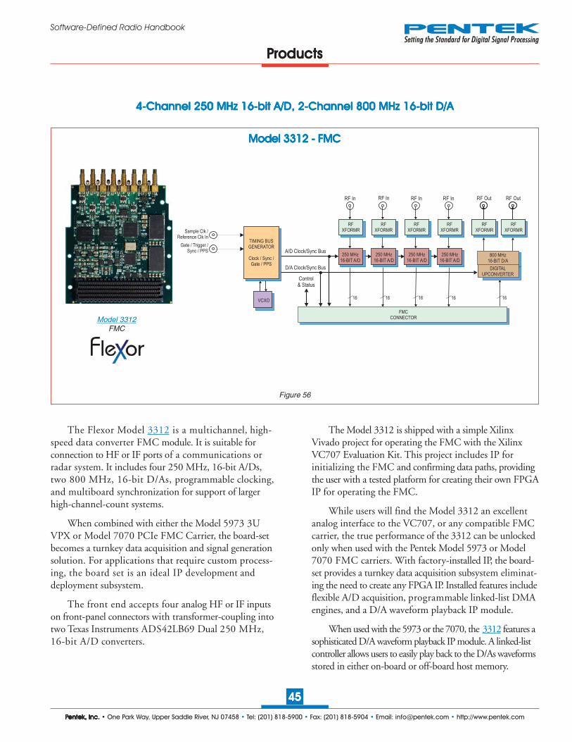
PPPPPentek, Inc.entek, Inc.entek, Inc.entek, Inc.entek, Inc. • One Park Way, Upper Saddle River, NJ 07458 • Tel: (201) 818-5900 • Fax: (201) 818-5904 • Email: [email protected] • http://www.pentek.com
4545454545
Software-Defined Radio Handbook
PPPPProductsroductsroductsroductsroducts
Figure 56
4-4-4-4-4-Channel 250 MHz 16-bit A/D, 2-Channel 250 MHz 16-bit A/D, 2-Channel 250 MHz 16-bit A/D, 2-Channel 250 MHz 16-bit A/D, 2-Channel 250 MHz 16-bit A/D, 2-Channel 800 MHz 16-bit D/AChannel 800 MHz 16-bit D/AChannel 800 MHz 16-bit D/AChannel 800 MHz 16-bit D/AChannel 800 MHz 16-bit D/A
Model 3312 - FMCModel 3312 - FMCModel 3312 - FMCModel 3312 - FMCModel 3312 - FMC
TIMING BUSGENERATOR
Clock / Sync /Gate / PPS
VCXO
250 MHz16-BIT A/D
RF In
RFXFORMR
RF In
RFXFORMR
250 MHz16-BIT A/D
Sample Clk /Reference Clk In
A/D Clock/Sync Bus
1616
RF In
RFXFORMR
250 MHz16-BIT A/D
16
RF In
RFXFORMR
250 MHz16-BIT A/D
16
Gate / Trigger /Sync / PPS
FMCCONNECTOR
Control& Status
RFXFORMR
800 MHz16-BIT D/A
DIGITALUPCONVERTER
RF Out
RFXFORMR
D/A Clock/Sync Bus
16
RFXFORMR
RF Out
RFXFORMR
Model 3312FMC
The Flexor Model 3312 is a multichannel, high-speed data converter FMC module. It is suitable forconnection to HF or IF ports of a communications orradar system. It includes four 250 MHz, 16-bit A/Ds,two 800 MHz, 16-bit D/As, programmable clocking,and multiboard synchronization for support of largerhigh-channel-count systems.
When combined with either the Model 5973 3UVPX or Model 7070 PCIe FMC Carrier, the board-setbecomes a turnkey data acquisition and signal generationsolution. For applications that require custom process-ing, the board set is an ideal IP development anddeployment subsystem.
The front end accepts four analog HF or IF inputson front-panel connectors with transformer-coupling intotwo Texas Instruments ADS42LB69 Dual 250 MHz,16-bit A/D converters.
The Model 3312 is shipped with a simple XilinxVivado project for operating the FMC with the XilinxVC707 Evaluation Kit. This project includes IP forinitializing the FMC and confirming data paths, providingthe user with a tested platform for creating their own FPGAIP for operating the FMC.
While users will find the Model 3312 an excellentanalog interface to the VC707, or any compatible FMCcarrier, the true performance of the 3312 can be unlockedonly when used with the Pentek Model 5973 or Model7070 FMC carriers. With factory-installed IP, the board-set provides a turnkey data acquisition subsystem eliminat-ing the need to create any FPGA IP. Installed features includeflexible A/D acquisition, programmable linked-list DMAengines, and a D/A waveform playback IP module.
When used with the 5973 or the 7070, the 3312 features asophisticated D/A waveform playback IP module. A linked-listcontroller allows users to easily play back to the D/As waveformsstored in either on-board or off-board host memory.

PPPPPentek, Inc.entek, Inc.entek, Inc.entek, Inc.entek, Inc. • One Park Way, Upper Saddle River, NJ 07458 • Tel: (201) 818-5900 • Fax: (201) 818-5904 • Email: [email protected] • http://www.pentek.com
4646464646
Software-Defined Radio Handbook
PPPPProductsroductsroductsroductsroducts
Figure 57
8-8-8-8-8-Channel 250 MHz 16-bit A/DChannel 250 MHz 16-bit A/DChannel 250 MHz 16-bit A/DChannel 250 MHz 16-bit A/DChannel 250 MHz 16-bit A/D
Model 3316 - FMCModel 3316 - FMCModel 3316 - FMCModel 3316 - FMCModel 3316 - FMC
Model 3316FMC
TIMING BUSGENERATOR
Clock / Sync /Gate / PPS
VCXO
250 MHz16-BIT A/D
RF In
RFXFORMRSample Clk /
Reference Clk In A/DClock/SyncBus
16
Gate / Trigger /Sync / PPS
Control& Status
250 MHz16-BIT A/D
RF In
RFXFORMR
16
250 MHz16-BIT A/D
RF In
RFXFORMR
16
250 MHz16-BIT A/D
RF In
RFXFORMR
16
250 MHz16-BIT A/D
RF In
RFXFORMR
16
250 MHz16-BIT A/D
RF In
RFXFORMR
16
250 MHz16-BIT A/D
RF In
RFXFORMR
16
250 MHz16-BIT A/D
RF In
RFXFORMR
16
FMCCONNECTOR
The Flexor Model 3316 is a multichannel, high-speed data converter FMC module. It is suitable forconnection to HF or IF ports of a communications orradar system. It includes four 250 MHz, 16-bit A/Ds,on-board programmable clocking, and multiboardsynchronization for support of larger high-channel-countsystems.
When combined with either the Model 5973 3UVPX or Model 7070 PCIe FMC Carrier, the board-setbecomes a turnkey data acquisition solution. Forapplications that require custom processing, the board-setis an ideal IP development and deployment subsystem
The front end accepts eight analog HF or IF inputson front-panel connectors with transformer-coupling intofour Texas Instruments ADS42LB69 Dual 250 MHz,16-bit A/D converters.
The Model 3316 is shipped with a simple XilinxVivado project for operating the FMC with the Xilinx
VC707 Evaluation Kit. This project includes IP forinitializing the FMC and confirming data paths, providingthe user with a tested platform for creating their own FPGAIP for operating the FMC.
While users will find the Model 3316 an excellentanalog interface to the VC707, or any compatible FMCcarrier, the true performance of the 3316 can be unlockedonly when used with the Pentek Model 5973 or Model7070 FMC carriers. With factory-installed IP, the board-set provides a turnkey data acquisition subsystem eliminat-ing the need to create any FPGA IP. Installed featuresinclude flexible A/D acquisition, programmable linked-list DMA engines, and a metadata packet creator.
When the 3316 is installed on either the 5973 orthe 7070 FMC carrier, the board-set features eight A/DAcquisition IP modules for easily capturing and movingdata. Each module can receive data from any of the eightA/Ds, or a test signal generator.

PPPPPentek, Inc.entek, Inc.entek, Inc.entek, Inc.entek, Inc. • One Park Way, Upper Saddle River, NJ 07458 • Tel: (201) 818-5900 • Fax: (201) 818-5904 • Email: [email protected] • http://www.pentek.com
4747474747
Software-Defined Radio Handbook
Figure 58
4-4-4-4-4-Channel 500 MHz 16-bit A/D, 4-Channel 500 MHz 16-bit A/D, 4-Channel 500 MHz 16-bit A/D, 4-Channel 500 MHz 16-bit A/D, 4-Channel 500 MHz 16-bit A/D, 4-Channel 2 GHz 16-bit D/AChannel 2 GHz 16-bit D/AChannel 2 GHz 16-bit D/AChannel 2 GHz 16-bit D/AChannel 2 GHz 16-bit D/A
Model 3324 - FMCModel 3324 - FMCModel 3324 - FMCModel 3324 - FMCModel 3324 - FMC
PPPPProductsroductsroductsroductsroducts
Model 3324FMC
TIMING BUSGENERATOR
Clock / Sync /Gate / PPS
VCXO
500 MHz16-BIT A/D
RF In
RFXFORMR
RF In
RFXFORMR
500 MHz16-BIT A/D
Sample Clk /Reference Clk In
A/DClock/SyncBus
RF In
RFXFORMR
500 MHz16-BIT A/D
RF In
RFXFORMR
500 MHz16-BIT A/D
Gate / Trigger /Sync / PPS
FMCCONNECTOR
Control& Status
RFXFORMR
2 GHz16-BIT D/A
DIGITALUPCONVERT
RF Out
RFXFORMR
RFXFORMR
2 GHz16-BIT D/A
DIGITALUPCONVERT
RF Out
RFXFORMR
RFXFORMR
RF Out
RFXFORMR
RFXFORMR
RF Out
RFXFORMR
D/AClock/SyncBus
2 GHz16-BIT D/A
2 GHz16-BIT D/A
DIGITALUPCONVERT
DIGITALUPCONVERT
DIGITALUPCONVERT
DIGITALUPCONVERT
DIGITALUPCONVERT
DIGITALUPCONVERT
The Flexor Model 3324 is a multichannel, high-speeddata converter FMC. It is suitable for connection to HF orIF ports of a communications or radar system. It includesfour 500 MHz, 16-bit A/Ds, four 2 GHz, 16-bit D/As,programmable clocking, and multi-board synchroniza-tion for support of larger high-channelcount systems.
When combined with either the Model 5973 3UVPX or Model 7070 PCIe FMC Carrier, the board-setbecomes a turnkey data acquisition solution. Forapplications that require custom processing, the board-setis an ideal IP development and deployment subsystem.
The front end accepts four analog HF or IF inputson front-panel connectors with transformer-coupling intofour 500 MHz, 16-bit A/D converters.
The Model 3324 is shipped with a simple Xilinx Vivadoproject for operating the FMC with the Xilinx VC707Evaluation Kit. This project includes IP for initializing theFMC and confirming data paths, providing the user with atested platform for creating their own IP for operating the FMC.
While users will find the Model 3324 an excellentanalog interface to the VC707 or any compatible FMCcarrier, the true performance of the 3324 can be unlockedonly when used with the Pentek Model 5973 or Model7070 FMC carriers. With factory-installed IP, the board setprovides a turnkey data acquisition and signal generationsubsystem, eliminating the need to create any FPGA IP.Installed features include flexible A/D acquisition engines, D/Awaveform playback engines, programmable linked-listDMA engines, and a metadata-packet creator.
The board-set features four A/D Acquisition IP Modulesfor easily capturing and moving data. Each module can receivedata from any of the four A/Ds, a test signal generator or fromthe D/A waveform playback IP module in loopback mode.
When used with a Pentek FMC carrier, the 3324features four sophisticated D/A waveform playback IPmodules. A linked-list controller allows users to easilyplay back via the D/As waveforms stored in either on-board or off-board host memory.

PPPPPentek, Inc.entek, Inc.entek, Inc.entek, Inc.entek, Inc. • One Park Way, Upper Saddle River, NJ 07458 • Tel: (201) 818-5900 • Fax: (201) 818-5904 • Email: [email protected] • http://www.pentek.com
4848484848
Software-Defined Radio Handbook
Figure 59
PPPPProductsroductsroductsroductsroducts
44444-----ChChChChChannelannelannelannelannel 2 2 2 2 25050505050 MHz MHz MHz MHz MHz A/DA/DA/DA/DA/D, 2-, 2-, 2-, 2-, 2-Channel 800 MHz D/A - 3U OpenVPXChannel 800 MHz D/A - 3U OpenVPXChannel 800 MHz D/A - 3U OpenVPXChannel 800 MHz D/A - 3U OpenVPXChannel 800 MHz D/A - 3U OpenVPX
FlexorSet Model 5973-312FlexorSet Model 5973-312FlexorSet Model 5973-312FlexorSet Model 5973-312FlexorSet Model 5973-312
PCIe INTERFACE
D/AWAVEFORMPLAYBACKIP MODULE
fromA/D Ch 1
fromA/D Ch 2
fromA/D Ch 3
fromA/D Ch 4
toD/A
GigabitSerial I/OPCIe
FPGAGPIO
D/A loopback
DETAILS OF VIRTEX-7 FPGA IPINSTALLED IN MODEL 5973-312DETAILS OF VIRTEX-7 FPGA IPINSTALLED IN MODEL 5973-312
A/DACQUISITIONIP MODULE 1
LINKED-LISTDMA ENGINE
DATAPACKING& FLOW
CONTROL
METADATAGENERATOR
MUX
A/DACQUISITIONIP MODULE 4
LINKED-LISTDMA ENGINE
DATAPACKING& FLOW
CONTROL
METADATAGENERATOR
MUX
INPUT MULTIPLEXER
DATAUNPACKING
& FLOWCONTROL
TESTSIGNAL
GENERATOR
MUX
LINKED-LISTDMA ENGINE
toMem
Bank 1
MEMORYCONTROL
toMem
Bank 4
MEMORYCONTROL
toMem
Bank 4
MEMORYCONTROL
8X 4X 32
A/DACQUISITIONIP MODULES
2 & 3
MemoryBank 4
32MemoryBank 3
32MemoryBank 2
32MemoryBank 1
32
toA/D AcqModule 1
toA/D AcqModule 2
toA/D AcqModule 3
toA/D AcqMod 4 &D/A Mod
See page 21
Model 5973-312
Model 5973-312 is a member of the Flexor family of high-performance 3U VPX boards based on the Xilinx Virtex-7 FPGA.
As a FlexorSet integrated solution, the Model 3312 FMC is factory-installed on the 5973 FMC carrier. The required FPGA IP is installed and the board set is delivered ready for immediate use.
The delivered FlexorSet is a multichannel, high-speeddata converter and is suitable for connection to the HF orIF ports of a communications or radar system. Its built-indata capture features offer an ideal turnkey solution as well asa platform for developing and deploying custom FPGA-processing IP.
It includes four 250 MHz, 16-bit A/Ds, one digitalupconverter, two 800 MHz, 16-bit D/As, and four banksof memory. In addition to supporting PCIe Gen. 3 as anative interface, the Model 5973-312 includes optionalcopper and optical connections to the Virtex-7 FPGA forcustom I/O.
When delivered as an assembled board set, the 5973-312includes factory-installed applications ideally matched tothe board’s analog interfaces. The functions include four A/Dacquisition IP modules for simplifying data capture and datatransfer. Each of the four acquisition IP modules contains IPmodules for DDR3 SDRAM memories.
The 5973-312 features a sophisticated D/A waveformplayback IP module. A linked-list controller allows users toeasily play back to the D/As waveforms stored in either on-board or off-board host memory. Parameters includinglength of waveform, delay from playback trigger, waveformrepetition, etc. can be programmed for each waveform. Upto 64 individual link entries can be chained together tocreate complex waveforms with a minimum of programming.
A controller for all data clocking and synchroniza-tion functions, a test signal generator, and a PCIeinterface complete the factory-installed functions andenable the 5973-312 to operate as a turnkey solutionwithout the need to develop any FPGA IP.
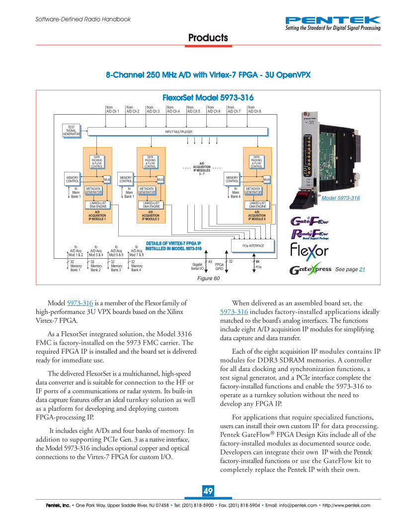
PPPPPentek, Inc.entek, Inc.entek, Inc.entek, Inc.entek, Inc. • One Park Way, Upper Saddle River, NJ 07458 • Tel: (201) 818-5900 • Fax: (201) 818-5904 • Email: [email protected] • http://www.pentek.com
4949494949
Software-Defined Radio Handbook
Figure 60
PPPPProductsroductsroductsroductsroducts
88888-----ChChChChChannelannelannelannelannel 2 2 2 2 25050505050 MHz MHz MHz MHz MHz A/DA/DA/DA/DA/D with Vir with Vir with Vir with Vir with Virtex-7 FPGA - 3U OpenVPXtex-7 FPGA - 3U OpenVPXtex-7 FPGA - 3U OpenVPXtex-7 FPGA - 3U OpenVPXtex-7 FPGA - 3U OpenVPX
FlexorSet Model 5973-316FlexorSet Model 5973-316FlexorSet Model 5973-316FlexorSet Model 5973-316FlexorSet Model 5973-316
PCIe INTERFACE
fromA/D Ch 1
PCIe
8X
DETAILS OF VIRTEX-7 FPGA IPINSTALLED IN MODEL 5973-316DETAILS OF VIRTEX-7 FPGA IPINSTALLED IN MODEL 5973-316
A/DACQUISITIONIP MODULE 1
A/DACQUISITIONIP MODULE 2
A/DACQUISITIONIP MODULE 8
LINKED-LISTDMA ENGINE
LINKED-LISTDMA ENGINE
LINKED-LISTDMA ENGINE
METADATAGENERATOR
METADATAGENERATOR
METADATAGENERATOR
toMem
Bank 1
toMem
Bank 1
toMem
Bank 4
MEMORYCONTROL
MEMORYCONTROL
MEMORYCONTROLMUX MUX MUX
INPUT MULTIPLEXER
DATAPACKING& FLOW
CONTROL
DATAPACKING& FLOW
CONTROL
DATAPACKING& FLOW
CONTROL
TESTSIGNAL
GENERATOR
8XFPGAGPIO
32MemoryBank 4
32MemoryBank 3
32MemoryBank 2
32MemoryBank 1
32
toA/D Acq
Mod 1 & 2
toA/D Acq
Mod 3 & 4
toA/D Acq
Mod 5 & 6
toA/D Acq
Mod 7 & 8
fromA/D Ch 2
fromA/D Ch 3
fromA/D Ch 4
fromA/D Ch 5
fromA/D Ch 6
fromA/D Ch 7
fromA/D Ch 8
A/DACQUISITIONIP MODULES
3 - 7
GigabitSerial I/O
4X
See page 21
Model 5973-316
Model 5973-316 is a member of the Flexor family of high-performance 3U VPX boards based on the Xilinx Virtex-7 FPGA.
As a FlexorSet integrated solution, the Model 3316 FMC is factory-installed on the 5973 FMC carrier. The required FPGA IP is installed and the board set is delivered ready for immediate use.
The delivered FlexorSet is a multichannel, high-speeddata converter and is suitable for connection to the HF orIF ports of a communications or radar system. Its built-indata capture features offer an ideal turnkey solution as wellas a platform for developing and deploying customFPGA-processing IP.
It includes eight A/Ds and four banks of memory. Inaddition to supporting PCIe Gen. 3 as a native interface,the Model 5973-316 includes optional copper and opticalconnections to the Virtex-7 FPGA for custom I/O.
When delivered as an assembled board set, the5973-316 includes factory-installed applications ideallymatched to the board’s analog interfaces. The functionsinclude eight A/D acquisition IP modules for simplifyingdata capture and data transfer.
Each of the eight acquisition IP modules contains IPmodules for DDR3 SDRAM memories. A controllerfor all data clocking and synchronization functions, atest signal generator, and a PCIe interface complete thefactory-installed functions and enable the 5973-316 tooperate as a turnkey solution without the need todevelop any FPGA IP.
For applications that require specialized functions,users can install their own custom IP for data processing.Pentek GateFlow® FPGA Design Kits include all of thefactory-installed modules as documented source code.Developers can integrate their own IP with the Pentekfactory-installed functions or use the GateFlow kit tocompletely replace the Pentek IP with their own.

PPPPPentek, Inc.entek, Inc.entek, Inc.entek, Inc.entek, Inc. • One Park Way, Upper Saddle River, NJ 07458 • Tel: (201) 818-5900 • Fax: (201) 818-5904 • Email: [email protected] • http://www.pentek.com
5050505050
Software-Defined Radio Handbook
88888-----ChChChChChannelannelannelannelannel 2 2 2 2 25050505050 MHz MHz MHz MHz MHz A/DA/DA/DA/DA/D with Digital Downconver with Digital Downconver with Digital Downconver with Digital Downconver with Digital Downconverters - 3U OpenVPXters - 3U OpenVPXters - 3U OpenVPXters - 3U OpenVPXters - 3U OpenVPX
Figure 61
See page 21
Model 5973-317
PCIe INTERFACE
fromA/D Ch 1
PCIe
8X
DETAILS OF VIRTEX-7 FPGA IPINSTALLED IN MODEL 5973-317DETAILS OF VIRTEX-7 FPGA IPINSTALLED IN MODEL 5973-317
A/DACQUISITIONIP MODULE 1
A/DACQUISITIONIP MODULE 2
A/DACQUISITIONIP MODULE 8
LINKED-LISTDMA ENGINE
LINKED-LISTDMA ENGINE
LINKED-LISTDMA ENGINE
METADATAGENERATOR
METADATAGENERATOR
METADATAGENERATORto
MemBank 1
MEMORYCONTROL
toMem
Bank 1
MEMORYCONTROL
toMem
Bank 4
MEMORYCONTROL
MUX MUX MUX
DATA PACKING &FLOW CONTROL
DATA PACKING &FLOW CONTROL
DATA PACKING &FLOW CONTROL
INPUT MULTIPLEXER
DDCDEC: 2 TO 65536
DDCDEC: 2 TO 65536
DDCDEC: 2 TO 65536
POWERMETER &
THRESHOLDDETECT
POWERMETER &
THRESHOLDDETECT
POWERMETER &
THRESHOLDDETECT
DDC CORE DDC CORE DDC CORE
TESTSIGNAL
GENERATOR
DATA PACKING &FLOW CONTROL
8XFPGAGPIO
32MemoryBank 4
32MemoryBank 3
32MemoryBank 2
32MemoryBank 1
32
toA/D Acq
Mod 1 & 2
toA/D Acq
Mod 3 & 4
toA/D Acq
Mod 5 & 6
toA/D Acq
Mod 7 & 8
fromA/D Ch 2
fromA/D Ch 3
fromA/D Ch 4
fromA/D Ch 5
fromA/D Ch 6
fromA/D Ch 7
fromA/D Ch 8
A/DACQUISITIONIP MODULES
3 - 7
GigabitSerial I/O
4X
PPPPProductsroductsroductsroductsroducts
FlexorSet Model 5973-317FlexorSet Model 5973-317FlexorSet Model 5973-317FlexorSet Model 5973-317FlexorSet Model 5973-317
Model 5973-317 is a member of the Flexor family ofhigh-performance 3U VPX boards based on the XilinxVirtex-7 FPGA.
As a FlexorSet integrated solution, the Model 3316FMC is factory-installed on the 5973 FMC carrier. Therequired FPGA IP is installed and the board set is deliveredready for immediate use.
The delivered FlexorSet is a multichannel, high-speeddata converter with programmable DDCs (DigitalDownconverters) and is suitable for connection to theHF or IF ports of a communications or radar system. Itsbuilt-in data capture features offer an ideal turnkey solutionas well as a platform for developing and deploying customFPGA-processing IP.
The Model 5973-317 includes eight A/Ds and fourbanks of memory. In addition to supporting PCIe Gen. 3as a native interface, it includes optional copper and opticalconnections to the Virtex-7 FPGA for custom I/O.
When delivered as an assembled board set, the5973-317 includes factory-installed applications ideallymatched to the board’s analog interfaces. The functionsinclude eight A/D acquisition IP modules for simplifyingdata capture and data transfer.
Within each A/D Acquisition IP Module is a powerfulDDC IP core. Each DDC has an independent 32-bittuning frequency setting that ranges from DC to ƒs, whereƒs is the A/D sampling frequency. Each DDC can haveits own unique decimation setting, supporting as many aseight different output bandwidths for the board. Decimationscan be programmed from 2 to 65,536 providing a wide rangeto satisfy most applications.
The decimating filter for each DDC accepts aunique set of user-supplied 18-bit coefficients. The 80%default filters deliver an output bandwidth of 0.8*ƒs/N,where N is the decimation setting. The rejection ofadjacent-band components within the 80% outputbandwidth is better than 100 dB.
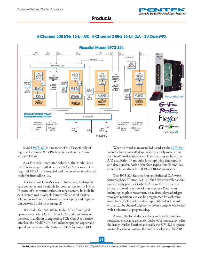
PPPPPentek, Inc.entek, Inc.entek, Inc.entek, Inc.entek, Inc. • One Park Way, Upper Saddle River, NJ 07458 • Tel: (201) 818-5900 • Fax: (201) 818-5904 • Email: [email protected] • http://www.pentek.com
5151515151
Software-Defined Radio Handbook
Figure 62
PPPPProductsroductsroductsroductsroducts
44444-----ChChChChChannelannelannelannelannel 500500500500500 MHz MHz MHz MHz MHz 16-bit 16-bit 16-bit 16-bit 16-bit A/DA/DA/DA/DA/D, 4-, 4-, 4-, 4-, 4-Channel 2 GHz 16-bit D/A - 3U OpenVPXChannel 2 GHz 16-bit D/A - 3U OpenVPXChannel 2 GHz 16-bit D/A - 3U OpenVPXChannel 2 GHz 16-bit D/A - 3U OpenVPXChannel 2 GHz 16-bit D/A - 3U OpenVPX
FlexorSet Model 5973-324FlexorSet Model 5973-324FlexorSet Model 5973-324FlexorSet Model 5973-324FlexorSet Model 5973-324
PCIe INTERFACE
D/AWAVEFORMPLAYBACK
IP MODULE 4
D/AWAVEFORMPLAYBACK
IP MODULE 1
FromA/D Ch 1
FromA/D Ch 2
FromA/D Ch 3
FromA/D Ch 4
ToD/A Ch 4
ToD/A Ch 1
ToD/A Ch 2
GigabitSerial I/OPCIe
FPGAGPIO
D/A loopback
D/A loopback
DETAILS OF VIRTEX-7 FPGA IPINSTALLED IN MODEL 5973-324DETAILS OF VIRTEX-7 FPGA IPINSTALLED IN MODEL 5973-324
A/DACQUISITIONIP MODULE 1
LINKED-LISTDMA ENGINE
DATAPACKING& FLOW
CONTROL
METADATAGENERATOR
MUX
A/DACQUISITIONIP MODULE 4
LINKED-LISTDMA ENGINE
DATAPACKING& FLOW
CONTROL
METADATAGENERATOR
MUX
INPUT MULTIPLEXER
DATAUNPACKING
& FLOWCONTROL
DATAUNPACKING
& FLOWCONTROL
TESTSIGNAL
GENERATOR
MUXMUX
LINKED-LISTDMA ENGINE
LINKED-LISTDMA ENGINE
toMem
Bank 1
MEMORYCONTROL
toMem
Bank 2
MEMORYCONTROL
toMem
Bank 4
toMem
Bank 3
MEMORYCONTROL
MEMORYCONTROL
8X 4X32
A/DACQUISITIONIP MODULES
2 & 3
2 goes toMem Bank 1
3 goes toMem Bank 2
MemoryBank 4
32MemoryBank 3
32MemoryBank 2
32MemoryBank 1
32
To A/D AcqModules 1 & 2
To A/D AcqModules 3 & 4
To D/A PlaybackModules 1 & 2
To D/A PlaybackModules 3 & 4
D/AWAFEFORMPLAYBACK
IP MODULES2 & 3
2 goes toMem Bank 3
3 goes toMem Bank 4
ToD/A Ch3
Model 5973-324
See page 21
Model 5973-324 is a member of the Flexor family ofhigh-performance 3U VPX boards based on the XilinxVirtex-7 FPGA.
As a FlexorSet integrated solution, the Model 3324FMC is factory-installed on the 5973 FMC carrier. Therequired FPGA IP is installed and the board set is deliveredready for immediate use.
The delivered FlexorSet is a multichannel, high-speeddata converter and is suitable for connection to the HF orIF ports of a communications or radar system. Its built-indata capture and playback features offer an ideal turnkeysolution as well as a platform for developing and deploy-ing custom FPGA-processing IP.
It includes four 500 MHz, 16-bit A/Ds, four digitalupconverters, four 2 GHz, 16-bit D/As, and four banks ofmemory. In addition to supporting PCIe Gen. 3 as a nativeinterface, the Model 5973-324 includes optional copper andoptical connections to the Virtex-7 FPGA for custom I/O.
When delivered as an assembled board set, the 5973-324includes factory-installed applications ideally matched tothe board’s analog interfaces. The functions include fourA/D acquisition IP modules for simplifying data captureand data transfer. Each of the four acquisition IP modulescontains IP modules for DDR3 SDRAM memories.
The 5973-324 features four sophisticated D/A wave-form playback IP modules. A linked-list controller allowsusers to easily play back to the D/As waveforms stored ineither on-board or off-board host memory. Parametersincluding length of waveform, delay from playback trigger,waveform repetition, etc. can be programmed for each wave-form. In each playback module, up to 64 individual linkentries can be chained together to create complex waveformswith a minimum of programming.
A controller for all data clocking and synchronizationfunctions, a test signal generator, and a PCIe interface completethe factory-installed functions and enable the 5973-324 to operateas a turnkey solution without the need to develop any FPGA IP.

PPPPPentek, Inc.entek, Inc.entek, Inc.entek, Inc.entek, Inc. • One Park Way, Upper Saddle River, NJ 07458 • Tel: (201) 818-5900 • Fax: (201) 818-5904 • Email: [email protected] • http://www.pentek.com
5252525252
Software-Defined Radio Handbook
Figure 63
44444-----ChChChChChannelannelannelannelannel 2 2 2 2 25050505050 MHz MHz MHz MHz MHz A/DA/DA/DA/DA/D, 2-, 2-, 2-, 2-, 2-Channel 800 MHz D/A - x8 PCIeChannel 800 MHz D/A - x8 PCIeChannel 800 MHz D/A - x8 PCIeChannel 800 MHz D/A - x8 PCIeChannel 800 MHz D/A - x8 PCIe
FlexorSet Model 7070-312FlexorSet Model 7070-312FlexorSet Model 7070-312FlexorSet Model 7070-312FlexorSet Model 7070-312
PCIe INTERFACE
D/AWAVEFORMPLAYBACKIP MODULE
fromA/D Ch 1
fromA/D Ch 2
fromA/D Ch 3
fromA/D Ch 4
toD/A
PCIeFPGAGPIO
D/A loopback
DETAILS OF VIRTEX-7 FPGA IPINSTALLED IN MODEL 7070-312DETAILS OF VIRTEX-7 FPGA IPINSTALLED IN MODEL 7070-312
A/DACQUISITIONIP MODULE 1
LINKED-LISTDMA ENGINE
DATAPACKING& FLOW
CONTROL
METADATAGENERATOR
MUX
A/DACQUISITIONIP MODULE 4
LINKED-LISTDMA ENGINE
DATAPACKING& FLOW
CONTROL
METADATAGENERATOR
MUX
INPUT MULTIPLEXER
DATAUNPACKING
& FLOWCONTROL
TESTSIGNAL
GENERATOR
MUX
LINKED-LISTDMA ENGINE
toMem
Bank 1
MEMORYCONTROL
toMem
Bank 4
MEMORYCONTROL
toMem
Bank 4
MEMORYCONTROL
8X 32
A/DACQUISITIONIP MODULES
2 & 3
MemoryBank 4
32MemoryBank 3
32MemoryBank 2
32MemoryBank 1
32
toA/D AcqModule 1
toA/D AcqModule 2
toA/D AcqModule 3
toA/D AcqMod 4 &D/A Mod
See page 21
Model 7070-312
Model 7070-312 is a member of the Flexor family of high-performance PCIe boards based on the Xilinx Virtex- 7 FPGA.
As a FlexorSet integrated solution, the Model 3312 FMC is factory-installed on the 5973 FMC carrier. The required FPGA IP is installed and the board set is delivered ready for immediate use.
The delivered FlexorSet is a multichannel, high-speeddata converter and is suitable for connection to the HF orIF ports of a communications or radar system. Its built-indata capture features offer an ideal turnkey solution as well asa platform for developing and deploying custom FPGA-processing IP.
It includes four 250 MHz, 16-bit A/Ds, one digitalupconverter, two 800 MHz, 16-bit D/As, and four banks ofmemory. In addition to supporting PCIe Gen. 3 as a nativeinterface, the Model 7070-312 includes optional copperand optical connections to the Virtex-7 FPGA for custom I/O.
When delivered as an assembled board set, the 7070-312includes factory-installed applications ideally matched tothe board’s analog interfaces. The functions include four A/Dacquisition IP modules for simplifying data capture and datatransfer. Each of the four acquisition IP modules containsIP modules for DDR3 SDRAM memories.
The 7070-312 features a sophisticated D/A waveformplayback IP module. A linked-list controller allows usersto easily play back to the D/As waveforms stored in eitheron-board or off-board host memory. Parameters includinglength of waveform, delay from playback trigger, waveformrepetition, etc. can be programmed for each waveform. Up to64 individual link entries can be chained together to createcomplex waveforms with a minimum of programming.
A controller for all data clocking and synchronizationfunctions, a test signal generator, and a PCIe interfacecomplete the factory-installed functions and enable the7070-312 to operate as a turnkey solution without theneed to develop any FPGA IP.
PPPPProductsroductsroductsroductsroducts

PPPPPentek, Inc.entek, Inc.entek, Inc.entek, Inc.entek, Inc. • One Park Way, Upper Saddle River, NJ 07458 • Tel: (201) 818-5900 • Fax: (201) 818-5904 • Email: [email protected] • http://www.pentek.com
5353535353
Software-Defined Radio Handbook
Figure 64
PPPPProductsroductsroductsroductsroducts
88888-----ChChChChChannelannelannelannelannel 2 2 2 2 25050505050 MHz MHz MHz MHz MHz A/DA/DA/DA/DA/D with Vir with Vir with Vir with Vir with Virtex-7 FPGA - x8 PCIetex-7 FPGA - x8 PCIetex-7 FPGA - x8 PCIetex-7 FPGA - x8 PCIetex-7 FPGA - x8 PCIe
FlexorSet Model 7070-316FlexorSet Model 7070-316FlexorSet Model 7070-316FlexorSet Model 7070-316FlexorSet Model 7070-316
PCIe INTERFACE
fromA/D Ch 1
PCIe
8X
DETAILS OF VIRTEX-7 FPGA IPINSTALLED IN MODEL 7070-316DETAILS OF VIRTEX-7 FPGA IPINSTALLED IN MODEL 7070-316
A/DACQUISITIONIP MODULE 1
A/DACQUISITIONIP MODULE 2
A/DACQUISITIONIP MODULE 8
LINKED-LISTDMA ENGINE
LINKED-LISTDMA ENGINE
LINKED-LISTDMA ENGINE
METADATAGENERATOR
METADATAGENERATOR
METADATAGENERATOR
toMem
Bank 1
toMem
Bank 1
toMem
Bank 4
MEMORYCONTROL
MEMORYCONTROL
MEMORYCONTROLMUX MUX MUX
INPUT MULTIPLEXER
DATAPACKING& FLOW
CONTROL
DATAPACKING& FLOW
CONTROL
DATAPACKING& FLOW
CONTROL
TESTSIGNAL
GENERATOR
8XFPGAGPIO
32MemoryBank 4
32MemoryBank 3
32MemoryBank 2
32MemoryBank 1
32
toA/D Acq
Mod 1 & 2
toA/D Acq
Mod 3 & 4
toA/D Acq
Mod 5 & 6
toA/D Acq
Mod 7 & 8
fromA/D Ch 2
fromA/D Ch 3
fromA/D Ch 4
fromA/D Ch 5
fromA/D Ch 6
fromA/D Ch 7
fromA/D Ch 8
A/DACQUISITIONIP MODULES
3 - 7
See page 21
Model 7070-316
Model 7070-316 is a member of the Flexor family of high-performance PCIe boards based on the Xilinx Virtex-7 FPGA.
As a FlexorSet integrated solution, the Model 3316 FMC is factory-installed on the 7070 FMC carrier. The required FPGA IP is installed and the board set is delivered ready for immediate use.
The delivered FlexorSet is a multichannel, high-speeddata converter and is suitable for connection to the HF orIF ports of a communications or radar system. Its built-indata capture features offer an ideal turnkey solution aswell as a platform for developing and deploying customFPGA-processing IP.
It includes eight A/Ds and four banks of memory. Inaddition to supporting PCIe Gen. 3 as a native interface,the Model 7070-316 includes optional copper and opticalconnections to the Virtex-7 FPGA for custom I/O.
When delivered as an assembled board set, the7070-316 includes factory-installed applications ideallymatched to the board’s analog interfaces. The functionsinclude eight A/D acquisition IP modules for simplifyingdata capture and data transfer.
Each of the eight acquisition IP modules contains IPmodules for DDR3 SDRAM memories. A controllerfor all data clocking and synchronization functions, atest signal generator, and a PCIe interface complete thefactory-installed functions and enable the 7070-316 tooperate as a turnkey solution without the need todevelop any FPGA IP.
For applications that require specialized functions,users can install their own custom IP for data processing.Pentek GateFlow® FPGA Design Kits include all of thefactory- installed modules as documented source code.Developers can integrate their own IP with the Pentekfactory-installed functions or use the GateFlow kit tocompletely replace the Pentek IP with their own.

PPPPPentek, Inc.entek, Inc.entek, Inc.entek, Inc.entek, Inc. • One Park Way, Upper Saddle River, NJ 07458 • Tel: (201) 818-5900 • Fax: (201) 818-5904 • Email: [email protected] • http://www.pentek.com
5454545454
Software-Defined Radio Handbook
88888-----ChChChChChannelannelannelannelannel 2 2 2 2 25050505050 MHz MHz MHz MHz MHz A/DA/DA/DA/DA/D with Digital Downconver with Digital Downconver with Digital Downconver with Digital Downconver with Digital Downconverters - x8 PCIeters - x8 PCIeters - x8 PCIeters - x8 PCIeters - x8 PCIe
See page 21
Model 7070-317
PPPPProductsroductsroductsroductsroducts
FlexorSet Model 7070-317FlexorSet Model 7070-317FlexorSet Model 7070-317FlexorSet Model 7070-317FlexorSet Model 7070-317
PCIe INTERFACE
fromA/D Ch 1
PCIe
8X
DETAILS OF VIRTEX-7 FPGA IPINSTALLED IN MODEL 7070-317DETAILS OF VIRTEX-7 FPGA IPINSTALLED IN MODEL 7070-317
A/DACQUISITIONIP MODULE 1
A/DACQUISITIONIP MODULE 2
A/DACQUISITIONIP MODULE 8
LINKED-LISTDMA ENGINE
LINKED-LISTDMA ENGINE
LINKED-LISTDMA ENGINE
METADATAGENERATOR
METADATAGENERATOR
METADATAGENERATORto
MemBank 1
MEMORYCONTROL
toMem
Bank 1
MEMORYCONTROL
toMem
Bank 4
MEMORYCONTROL
MUX MUX MUX
DATA PACKING &FLOW CONTROL
DATA PACKING &FLOW CONTROL
DATA PACKING &FLOW CONTROL
INPUT MULTIPLEXER
DDCDEC: 2 TO 65536
DDCDEC: 2 TO 65536
DDCDEC: 2 TO 65536
POWERMETER &
THRESHOLDDETECT
POWERMETER &
THRESHOLDDETECT
POWERMETER &
THRESHOLDDETECT
DDC CORE DDC CORE DDC CORE
TESTSIGNAL
GENERATOR
DATA PACKING &FLOW CONTROL
8XFPGAGPIO
32MemoryBank 4
32MemoryBank 3
32MemoryBank 2
32MemoryBank 1
32
toA/D Acq
Mod 1 & 2
toA/D Acq
Mod 3 & 4
toA/D Acq
Mod 5 & 6
toA/D Acq
Mod 7 & 8
fromA/D Ch 2
fromA/D Ch 3
fromA/D Ch 4
fromA/D Ch 5
fromA/D Ch 6
fromA/D Ch 7
fromA/D Ch 8
A/DACQUISITIONIP MODULES
3 - 7
Figure 65
Model 7070-317 is a member of the Flexor family ofhigh-performance PCIe boards based on the Xilinx Virtex-7 FPGA.
As a FlexorSet integrated solution, the Model 3316FMC is factory-installed on the 7070 FMC carrier. Therequired FPGA IP is installed and the board set is deliveredready for immediate use.
The delivered FlexorSet is a multichannel, high-speeddata converter with programmable DDCs (DigitalDownconverters) and is suitable for connection to theHF or IF ports of a communications or radar system. Itsbuilt-in data capture features offer an ideal turnkey solutionas well as a platform for developing and deploying customFPGA-processing IP.
It includes eight A/Ds and four banks of memory. Inaddition to supporting PCIe Gen. 3 as a native interface,the Model 7070-317 includes optional copper and opticalconnections to the Virtex-7 FPGA for custom I/O.
When delivered as an assembled board set, the7070-317 includes factory-installed applications ideallymatched to the board’s analog interfaces. The functionsinclude eight A/D acquisition IP modules for simplifyingdata capture and data transfer.
Within each A/D Acquisition IP Module is a powerfulDDC IP core. Each DDC has an independent 32-bittuning frequency setting that ranges from DC to ƒs, whereƒs is the A/D sampling frequency. Each DDC can haveits own unique decimation setting, supporting as many aseight different output bandwidths for the board. Decimationscan be programmed from 2 to 65,536 providing a wide rangeto satisfy most applications.
The decimating filter for each DDC accepts aunique set of user-supplied 18-bit coefficients. The 80%default filters deliver an output bandwidth of 0.8*ƒs/N,where N is the decimation setting. The rejection ofadjacent-band components within the 80% outputbandwidth is better than 100 dB.
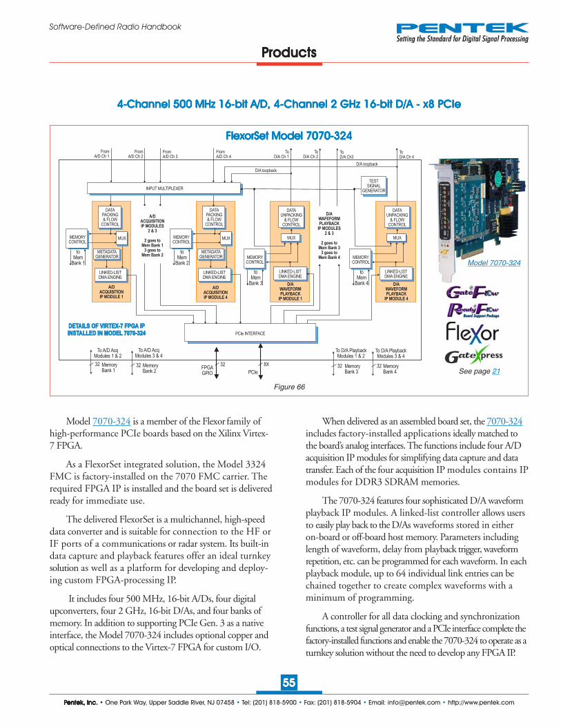
PPPPPentek, Inc.entek, Inc.entek, Inc.entek, Inc.entek, Inc. • One Park Way, Upper Saddle River, NJ 07458 • Tel: (201) 818-5900 • Fax: (201) 818-5904 • Email: [email protected] • http://www.pentek.com
5555555555
Software-Defined Radio Handbook
Figure 66
PPPPProductsroductsroductsroductsroducts
44444-----ChChChChChannelannelannelannelannel 500500500500500 MHz MHz MHz MHz MHz 16-bit 16-bit 16-bit 16-bit 16-bit A/DA/DA/DA/DA/D, 4-, 4-, 4-, 4-, 4-Channel 2 GHz 16-bit D/A - x8 PCIeChannel 2 GHz 16-bit D/A - x8 PCIeChannel 2 GHz 16-bit D/A - x8 PCIeChannel 2 GHz 16-bit D/A - x8 PCIeChannel 2 GHz 16-bit D/A - x8 PCIe
FlexorSet Model 7070-324FlexorSet Model 7070-324FlexorSet Model 7070-324FlexorSet Model 7070-324FlexorSet Model 7070-324
PCIe INTERFACE
D/AWAVEFORMPLAYBACK
IP MODULE 4
D/AWAVEFORMPLAYBACK
IP MODULE 1
FromA/D Ch 1
FromA/D Ch 2
FromA/D Ch 3
FromA/D Ch 4
ToD/A Ch 4
ToD/A Ch 1
ToD/A Ch 2
PCIeFPGAGPIO
D/A loopback
D/A loopback
DETAILS OF VIRTEX-7 FPGA IPINSTALLED IN MODEL 7070-324DETAILS OF VIRTEX-7 FPGA IPINSTALLED IN MODEL 7070-324
A/DACQUISITIONIP MODULE 1
LINKED-LISTDMA ENGINE
DATAPACKING& FLOW
CONTROL
METADATAGENERATOR
MUX
A/DACQUISITIONIP MODULE 4
LINKED-LISTDMA ENGINE
DATAPACKING& FLOW
CONTROL
METADATAGENERATOR
MUX
INPUT MULTIPLEXER
DATAUNPACKING
& FLOWCONTROL
DATAUNPACKING
& FLOWCONTROL
TESTSIGNAL
GENERATOR
MUXMUX
LINKED-LISTDMA ENGINE
LINKED-LISTDMA ENGINE
toMem
Bank 1
MEMORYCONTROL
toMem
Bank 2
MEMORYCONTROL
toMem
Bank 4
toMem
Bank 3
MEMORYCONTROL
MEMORYCONTROL
8X32
A/DACQUISITIONIP MODULES
2 & 3
2 goes toMem Bank 1
3 goes toMem Bank 2
MemoryBank 4
32MemoryBank 3
32MemoryBank 2
32MemoryBank 1
32
To A/D AcqModules 1 & 2
To A/D AcqModules 3 & 4
To D/A PlaybackModules 1 & 2
To D/A PlaybackModules 3 & 4
D/AWAFEFORMPLAYBACK
IP MODULES2 & 3
2 goes toMem Bank 3
3 goes toMem Bank 4
ToD/A Ch3
Model 7070-324
See page 21
Model 7070-324 is a member of the Flexor family ofhigh-performance PCIe boards based on the Xilinx Virtex-7 FPGA.
As a FlexorSet integrated solution, the Model 3324FMC is factory-installed on the 7070 FMC carrier. Therequired FPGA IP is installed and the board set is deliveredready for immediate use.
The delivered FlexorSet is a multichannel, high-speeddata converter and is suitable for connection to the HF orIF ports of a communications or radar system. Its built-indata capture and playback features offer an ideal turnkeysolution as well as a platform for developing and deploy-ing custom FPGA-processing IP.
It includes four 500 MHz, 16-bit A/Ds, four digitalupconverters, four 2 GHz, 16-bit D/As, and four banks ofmemory. In addition to supporting PCIe Gen. 3 as a nativeinterface, the Model 7070-324 includes optional copper andoptical connections to the Virtex-7 FPGA for custom I/O.
When delivered as an assembled board set, the 7070-324includes factory-installed applications ideally matched tothe board’s analog interfaces. The functions include four A/Dacquisition IP modules for simplifying data capture and datatransfer. Each of the four acquisition IP modules contains IPmodules for DDR3 SDRAM memories.
The 7070-324 features four sophisticated D/A waveformplayback IP modules. A linked-list controller allows usersto easily play back to the D/As waveforms stored in eitheron-board or off-board host memory. Parameters includinglength of waveform, delay from playback trigger, waveformrepetition, etc. can be programmed for each waveform. In eachplayback module, up to 64 individual link entries can bechained together to create complex waveforms with aminimum of programming.
A controller for all data clocking and synchronizationfunctions, a test signal generator and a PCIe interface complete thefactory-installed functions and enable the 7070-324 to operate as aturnkey solution without the need to develop any FPGA IP.

PPPPPentek, Inc.entek, Inc.entek, Inc.entek, Inc.entek, Inc. • One Park Way, Upper Saddle River, NJ 07458 • Tel: (201) 818-5900 • Fax: (201) 818-5904 • Email: [email protected] • http://www.pentek.com
5656565656
Software-Defined Radio Handbook
PPPPProductsroductsroductsroductsroducts
Model 8266 Model 8266 Model 8266 Model 8266 Model 8266
Figure 67
PC Development System for PCIe Cobalt, Onyx and Flexor BoardsPC Development System for PCIe Cobalt, Onyx and Flexor BoardsPC Development System for PCIe Cobalt, Onyx and Flexor BoardsPC Development System for PCIe Cobalt, Onyx and Flexor BoardsPC Development System for PCIe Cobalt, Onyx and Flexor Boards
The Model 8266 is a fully-integrated PC develop-ment system for Pentek Cobalt, Onyx and Flexor PCIExpress software radio, data acquisition, and I/O boards.It was created to save engineers and system integratorsthe time and expense associated with building and testing adevelopment system that ensures optimum performanceof Pentek boards.
A fully-integrated system-level solution, the 8266provides the user with a streamlined out-of-the-boxexperience. It comes preconfigured with Pentek hardware,drivers and software examples installed and tested to allowdevelopment engineers to run example applications outof the box.
Pentek ReadyFlow drivers and board supportlibraries are preinstalled and tested with the 8266.ReadyFlow includes example applications with fullsource code, a command line interface for custom
control over hardware, and Pentek’s Signal Analyzer, afull-featured analysis tool that continuously displays livesignals in both time and frequency domains.
Built on a professional 4U rackmount workstation,the 8266 is equipped with the latest Intel processor,DDR3 SDRAM and a high-performance motherboard.These features accelerate application code developmentand provide unhindered access to the high-bandwidthdata available with Cobalt, Onyx and Flexor analog anddigital interfaces. The 8266 can be configured with64-bit Windows or Linux operating systems.
The 8266 uses a 19” 4U rackmount chassis thatis 21” deep. Enhanced forced-air ventilation assuresadequate cooling for Pentek boards. A 1000-W powersupply guarantees more than enough power for addi-tional boards.
Model 8266
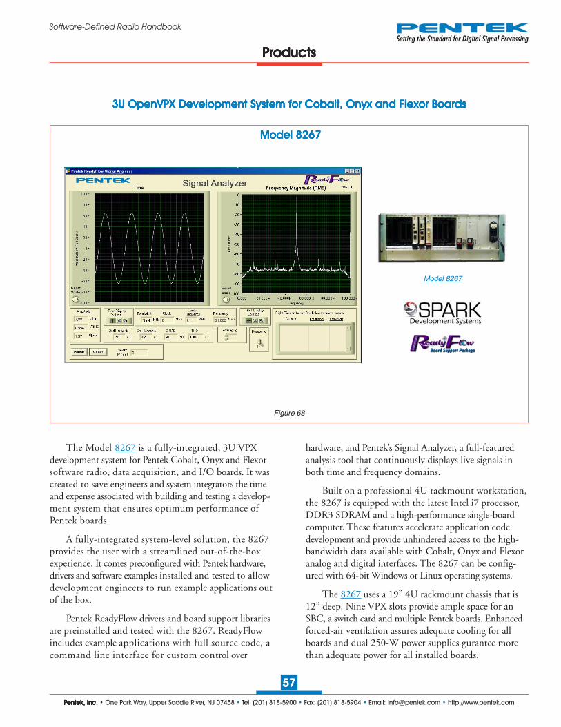
PPPPPentek, Inc.entek, Inc.entek, Inc.entek, Inc.entek, Inc. • One Park Way, Upper Saddle River, NJ 07458 • Tel: (201) 818-5900 • Fax: (201) 818-5904 • Email: [email protected] • http://www.pentek.com
5757575757
Software-Defined Radio Handbook
PPPPProductsroductsroductsroductsroducts
Model 8267 Model 8267 Model 8267 Model 8267 Model 8267
Figure 68
3U OpenVPX Development System for Cobalt, Onyx and Flexor Boards3U OpenVPX Development System for Cobalt, Onyx and Flexor Boards3U OpenVPX Development System for Cobalt, Onyx and Flexor Boards3U OpenVPX Development System for Cobalt, Onyx and Flexor Boards3U OpenVPX Development System for Cobalt, Onyx and Flexor Boards
Model 8267
The Model 8267 is a fully-integrated, 3U VPXdevelopment system for Pentek Cobalt, Onyx and Flexorsoftware radio, data acquisition, and I/O boards. It wascreated to save engineers and system integrators the timeand expense associated with building and testing a develop-ment system that ensures optimum performance ofPentek boards.
A fully-integrated system-level solution, the 8267provides the user with a streamlined out-of-the-boxexperience. It comes preconfigured with Pentek hardware,drivers and software examples installed and tested to allowdevelopment engineers to run example applications outof the box.
Pentek ReadyFlow drivers and board support librariesare preinstalled and tested with the 8267. ReadyFlowincludes example applications with full source code, acommand line interface for custom control over
hardware, and Pentek’s Signal Analyzer, a full-featuredanalysis tool that continuously displays live signals inboth time and frequency domains.
Built on a professional 4U rackmount workstation,the 8267 is equipped with the latest Intel i7 processor,DDR3 SDRAM and a high-performance single-boardcomputer. These features accelerate application codedevelopment and provide unhindered access to the high-bandwidth data available with Cobalt, Onyx and Flexoranalog and digital interfaces. The 8267 can be config-ured with 64-bit Windows or Linux operating systems.
The 8267 uses a 19” 4U rackmount chassis that is12” deep. Nine VPX slots provide ample space for anSBC, a switch card and multiple Pentek boards. Enhancedforced-air ventilation assures adequate cooling for allboards and dual 250-W power supplies gurantee morethan adequate power for all installed boards.
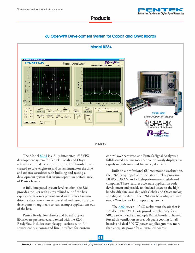
PPPPPentek, Inc.entek, Inc.entek, Inc.entek, Inc.entek, Inc. • One Park Way, Upper Saddle River, NJ 07458 • Tel: (201) 818-5900 • Fax: (201) 818-5904 • Email: [email protected] • http://www.pentek.com
5858585858
Software-Defined Radio Handbook
PPPPProductsroductsroductsroductsroducts
Model 8264 Model 8264 Model 8264 Model 8264 Model 8264
Figure 69
6U OpenVPX Development System for Cobalt and Onyx Boards6U OpenVPX Development System for Cobalt and Onyx Boards6U OpenVPX Development System for Cobalt and Onyx Boards6U OpenVPX Development System for Cobalt and Onyx Boards6U OpenVPX Development System for Cobalt and Onyx Boards
Model 8264
with 6U OpenVPX Boards
The Model 8264 is a fully-integrated, 6U VPXdevelopment system for Pentek Cobalt and Onyxsoftware radio, data acquisition, and I/O boards. It wascreated to save engineers and system integrators the timeand expense associated with building and testing adevelopment system that ensures optimum performanceof Pentek boards.
A fully-integrated system-level solution, the 8264provides the user with a streamlined out-of-the-boxexperience. It comes preconfigured with Pentek hardware,drivers and software examples installed and tested to allowdevelopment engineers to run example applications outof the box.
Pentek ReadyFlow drivers and board supportlibraries are preinstalled and tested with the 8264.ReadyFlow includes example applications with fullsource code, a command line interface for custom
control over hardware, and Pentek’s Signal Analyzer, afull-featured analysis tool that continuously displays livesignals in both time and frequency domains.
Built on a professional 6U rackmount workstation,the 8264 is equipped with the latest Intel i7 processor,DDR3 SDRAM and a high-performance single-boardcomputer. These features accelerate application codedevelopment and provide unhindered access to the high-bandwidth data available with Cobalt and Onyx analogand digital interfaces. The 8264 can be configured with64-bit Windows or Linux operating systems.
The 8264 uses a 19” 6U rackmount chassis that is12” deep. Nine VPX slots provide ample space for anSBC, a switch card and multiple Pentek boards. Enhancedforced-air ventilation assures adequate cooling for allboards and dual 500-W power supplies gurantee morethan adequate power for all installed boards.
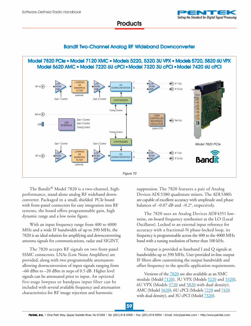
PPPPPentek, Inc.entek, Inc.entek, Inc.entek, Inc.entek, Inc. • One Park Way, Upper Saddle River, NJ 07458 • Tel: (201) 818-5900 • Fax: (201) 818-5904 • Email: [email protected] • http://www.pentek.com
5959595959
Software-Defined Radio Handbook
Bandit TBandit TBandit TBandit TBandit Twowowowowo-----Channel Analog RF WChannel Analog RF WChannel Analog RF WChannel Analog RF WChannel Analog RF Wideband Downconverideband Downconverideband Downconverideband Downconverideband Downconverterterterterter
Model 7820 PCIe Model 7820 PCIe Model 7820 PCIe Model 7820 PCIe Model 7820 PCIe ●●●●● Model 7120 XMC Model 7120 XMC Model 7120 XMC Model 7120 XMC Model 7120 XMC ●●●●● Models 5220, 5320 3U VPX Models 5220, 5320 3U VPX Models 5220, 5320 3U VPX Models 5220, 5320 3U VPX Models 5220, 5320 3U VPX ●●●●● Models 57Models 57Models 57Models 57Models 572020202020, 58, 58, 58, 58, 582020202020 6U VPX 6U VPX 6U VPX 6U VPX 6U VPXModel 5620 AMC Model 5620 AMC Model 5620 AMC Model 5620 AMC Model 5620 AMC ●●●●● Model 7220 6U cPCI Model 7220 6U cPCI Model 7220 6U cPCI Model 7220 6U cPCI Model 7220 6U cPCI ● ● ● ● ● Model 7320 3U cPCI Model 7320 3U cPCI Model 7320 3U cPCI Model 7320 3U cPCI Model 7320 3U cPCI ● ● ● ● ● Model 7420 6U cPCIModel 7420 6U cPCIModel 7420 6U cPCIModel 7420 6U cPCIModel 7420 6U cPCI
Figure 70
PPPPProductsroductsroductsroductsroducts
RF In
USB
I/QDOWNCONVERTER
SYNTHESIZER
Ref In
RF InI/Q
DOWNCONVERTER
SYNTHESIZER
I
Q
I
Q
Gain 1 Control
Gain 2 Control
Tuning Control
USBINTERFACE
Gain 1 Control
Gain 1 Control
Tuning Control
Tuning Control
IF I Out
IF Q Out
IF I Out
IF Q Out
(option 015)
Ref Out
OVENCONTROLLEDREFERENCEOSCILLATOR
(optional)
LOWPASSOR
BANDPASSFILTER
Gain 2 Control
(optional)
LOWPASSOR
BANDPASSFILTER
Gain 2 Control
LOWNOISEAMP
LOWNOISEAMP
LOWNOISEAMP
LOWNOISEAMP
LOWNOISEAMP
LOWNOISEAMP
Model 7820 PCIe
The Bandit® Model 7820 is a two-channel, high-performance, stand-alone analog RF wideband down-converter. Packaged in a small, shielded PCIe boardwith front-panel connectors for easy integration into RFsystems, the board offers programmable gain, highdynamic range and a low noise figure.
With an input frequency range from 400 to 4000MHz and a wide IF bandwidth of up to 390 MHz, the7820 is an ideal solution for amplifying and downconvertingantenna signals for communications, radar and SIGINT.
The 7820 accepts RF signals on two front-panelSSMC connectors. LNAs (Low Noise Amplifiers) areprovided, along with two programmable attenuatorsallowing downconversion of input signals ranging from–60 dBm to –20 dBm in steps of 0.5 dB. Higher levelsignals can be attenuated prior to input. An optionalfive-stage lowpass or bandpass input filter can beincluded with several available frequency and attenuationcharacteristics for RF image rejection and harmonic
suppression. The 7820 features a pair of AnalogDevices ADL5380 quadrature mixers. The ADL5380’sare capable of excellent accuracy with amplitude and phasebalances of ~0.07 dB and ~0.2°, respectively.
The 7820 uses an Analog Devices ADF4351 low-noise, on-board frequency synthesizer as the LO (LocalOscillator). Locked to an external input reference foraccuracy with a fractional-N phase-locked loop, itsfrequency is programmable across the 400 to the 4000 MHzband with a tuning resolution of better than 100 kHz.
Output is provided as baseband I and Q signals atbandwidths up to 390 MHz. User-provided in-line outputIF filters allow customizing the output bandwidth andoffset frequency to the specific application requirements.
Versions of the 7820 are also available as an XMCmodule (Model 7120), 3U VPX (Models 5220 and 5320),6U VPX (Models 5720 and 5820 with dual density),AMC (Model 5620), 6U cPCI (Models 7220 and 7420with dual density), and 3U cPCI (Model 7320).

PPPPPentek, Inc.entek, Inc.entek, Inc.entek, Inc.entek, Inc. • One Park Way, Upper Saddle River, NJ 07458 • Tel: (201) 818-5900 • Fax: (201) 818-5904 • Email: [email protected] • http://www.pentek.com
6060606060
Software-Defined Radio Handbook
RF SWITCH
RF In IF Out
RefIn
ExtLOIn
BANDPASSFILTER
STEPATTENUATOR
STEPATTENUATOR
MIXER IF FILTER
RF Attenuation
IF Attenuation
LO Select
LO Synthesizer Tuning Frequency
USBINTERFACE
LOWNOISEAMP
GAINBLOCK
GAINBLOCK
GAINBLOCK
GAINBLOCK
ControlIn
OVENCONTROLLED
CRYSTALOSCILLATOR
RefOut
LO
PPPPProductsroductsroductsroductsroducts
Model 8111 Model 8111 Model 8111 Model 8111 Model 8111
Figure 71
Bandit Modular Analog RF DownconverBandit Modular Analog RF DownconverBandit Modular Analog RF DownconverBandit Modular Analog RF DownconverBandit Modular Analog RF Downconverter Seriester Seriester Seriester Seriester Series
The Bandit Model 8111 provides a series of high-perfor-mance, stand-alone RF slot receiver modules. Packaged ina small, shielded enclosure with connectors for easyintegration into RF systems, the modules offer programmablegain, high dynamic range and a low noise figure. Withinput options to cover specific frequency bands of the RFspectrum, and an IF output optimized for A/D converters,the 8111 is an ideal solution for amplifying and down-converting antenna signals for communications, radar andsignal intelligence systems.
The 8111 accepts RF signals on a front panel SMAconnector. An LNA (Low Noise-figure Amplifier) isprovided along with two programmable attenuatorsallowing downconversion of input signals ranging from–60 dBm to –20 dBm in steps of 0.5 dB. Higher levelsignals can be attenuated prior to input.
Seven different input-frequency band options areoffered, each tunable across a 400 MHz band, with anoverlap of 100 MHz between adjacent bands. As agroup, these seven options accommodate RF inputsignals from 800 MHz to 3.000 GHz as follows:
Option Frequency Band001 800-1200 MHz002 1100-1500 MHz003 1400-1800 MHz004 1700-2100 MHz005 2000-2400 MHz006 2300-2700 MHz007 2600-3000 MHz
An 80 MHz wide IF output is provided at a 225 MHzcenter frequency . This output is suitable for A/D conver-sion using Pentek high-performance signal acquisitionproducts, such as those in the Cobalt and Onyx families.
Model 8111

PPPPPentek, Inc.entek, Inc.entek, Inc.entek, Inc.entek, Inc. • One Park Way, Upper Saddle River, NJ 07458 • Tel: (201) 818-5900 • Fax: (201) 818-5904 • Email: [email protected] • http://www.pentek.com
6161616161
Software-Defined Radio Handbook
ReferenceIn
Control
PCI INTERFACE
PCI BUS(32 Bits / 66 MHz)32
Clock Out1
Clock Out2
Clock Out3
Clock Out4
Clock Out5
Clock Out6
Clock Out7
Clock Out8
CLOCKSYNTHESIZER
AND JITTERCLEANER
A
1÷÷ 2÷ 4÷ 8÷16
QUADVCXO
A
CLOCKSYNTHESIZER
AND JITTERCLEANER
B
1÷÷ 2÷ 4÷ 8÷16
CLOCKSYNTHESIZER
AND JITTERCLEANER
C
1÷÷ 2÷ 4÷ 8÷16
CLOCKSYNTHESIZER
AND JITTERCLEANER
D
1÷÷ 2÷ 4÷ 8÷16
Supports:any In to any Out,any In to multiple
Outs
CROSSBAR
SWITCH
In
In
In
In
Out
Out
Out
Out
Out
QUADVCXO
B
QUADVCXO
C
QUADVCXO
D
PPPPProductsroductsroductsroductsroducts
Figure 72
Multifrequency Clock SynthesizerMultifrequency Clock SynthesizerMultifrequency Clock SynthesizerMultifrequency Clock SynthesizerMultifrequency Clock Synthesizer
Model 7190PMC
Model 7190 generates up to eight synthesized clocksignals suitable for driving A/D and D/A converters inhigh-performance real-time data acquisition and softwareradio systems. The clocks offer exceptionally low phase noiseand jitter to preserve the signal quality of the data converters.These clocks are synthesized from on-board quad VCXOsand can be phase-locked to an external reference signal.
The 7190 uses four Texas Instruments CDC7005 clocksynthesizer and jitter cleaner devices. Each CDC7005 is pairedwith a dedicated VCXO to provide the base frequency forthe clock synthesizer. Each of the four VCXOs can beindependently programmed to generate one of four frequen-cies between 50 MHz and 700 MHz.
The CDC7005 can output the selected frequencyof its associated VCXO, or generate submultiples usingdivisors of 2, 4, 8 or 16. The four CDC7005’s can outputup to five frequencies each. The 7190 can be programmed toroute any of these 20 frequencies to the module’s fiveoutput drivers.
The CDC7005 includes phase-locking circuitrythat locks the frequency of its associated VCXO to aninput reference of 5 MHz to 100 MHz.
Eight front panel SMC connectors supply synthesizedclock outputs driven from the five clock output drivers.This supports a single identical clock to all eight outputsor up to five different clocks to various outputs. Withfour independent quad VCXOs and each CDC7005capable of providing up to five different submultipleclocks, a wide range of clock configurations is possible. Insystems where more than five different clock outputs arerequired simultaneously, multiple 7190’s can be used andphase-locked with the 5 MHz to 100 MHz system reference.
Versions of the 7190 are also available as a PCIe half-length board (Model 7890), 3U VPX board (Model5390), 6U VPX (Models 5790 and 5890 with dualdensity), AMC (Model 5690) PCI board (Model 7690),6U cPCI (Models 7290 and 7290D dual density), or 3UcPCI (Model 7390).
Model 7190 PMC Model 7190 PMC Model 7190 PMC Model 7190 PMC Model 7190 PMC ●●●●● Model 7890 PCIe Model 7890 PCIe Model 7890 PCIe Model 7890 PCIe Model 7890 PCIe ●●●●● Model 5390 3U VPX Model 5390 3U VPX Model 5390 3U VPX Model 5390 3U VPX Model 5390 3U VPX ●●●●● Models 5790, 5890 6U VPX Models 5790, 5890 6U VPX Models 5790, 5890 6U VPX Models 5790, 5890 6U VPX Models 5790, 5890 6U VPXModel 5690 AMC Model 5690 AMC Model 5690 AMC Model 5690 AMC Model 5690 AMC ●●●●● Model 7690 PCI Model 7690 PCI Model 7690 PCI Model 7690 PCI Model 7690 PCI ● ● ● ● ● Model 7290 6U cPCI Model 7290 6U cPCI Model 7290 6U cPCI Model 7290 6U cPCI Model 7290 6U cPCI ●●●●● Model 7390 3U cPCI Model 7390 3U cPCI Model 7390 3U cPCI Model 7390 3U cPCI Model 7390 3U cPCI ●●●●●

PPPPPentek, Inc.entek, Inc.entek, Inc.entek, Inc.entek, Inc. • One Park Way, Upper Saddle River, NJ 07458 • Tel: (201) 818-5900 • Fax: (201) 818-5904 • Email: [email protected] • http://www.pentek.com
6262626262
Software-Defined Radio Handbook
ReferenceIn
Control
PCI INTERFACE
PCI BUS(32 Bits / 66 MHz)32
Clock Out1
Clock Out2
Clock Out3
Clock Out4
Clock Out5
Clock Out6
Clock Out7
Clock Out8
CLOCKSYNTHESIZER
AND JITTERCLEANER
A
1÷÷ 2÷ 4÷ 8÷16
PROGRAMVCXO
A
CLOCKSYNTHESIZER
AND JITTERCLEANER
B
1÷÷ 2÷ 4÷ 8÷16
CLOCKSYNTHESIZER
AND JITTERCLEANER
C
1÷÷ 2÷ 4÷ 8÷16
CLOCKSYNTHESIZER
AND JITTERCLEANER
D
1÷÷ 2÷ 4÷ 8÷16
Supports:any In to any Out,any In to multiple
Outs
CROSSBAR
SWITCH
In
In
In
In
Out
Out
Out
Out
Out
PROGRAMVCXO
B
PROGRAMVCXO
C
PROGRAMVCXO
D
PPPPProductsroductsroductsroductsroducts
Figure 73
Model 7191 PMC Model 7191 PMC Model 7191 PMC Model 7191 PMC Model 7191 PMC ●●●●● Model 7891 PCIe Model 7891 PCIe Model 7891 PCIe Model 7891 PCIe Model 7891 PCIe ●●●●● Model 5391 3U VPX Model 5391 3U VPX Model 5391 3U VPX Model 5391 3U VPX Model 5391 3U VPX ●●●●● Models 5791, 5891 6U VPX Models 5791, 5891 6U VPX Models 5791, 5891 6U VPX Models 5791, 5891 6U VPX Models 5791, 5891 6U VPXModel 5691 AMC Model 5691 AMC Model 5691 AMC Model 5691 AMC Model 5691 AMC ●●●●● Model 7691 PCI Model 7691 PCI Model 7691 PCI Model 7691 PCI Model 7691 PCI ● ● ● ● ● Model 7291 6U cPCI Model 7291 6U cPCI Model 7291 6U cPCI Model 7291 6U cPCI Model 7291 6U cPCI ●●●●● Model 7391 3U cPCI Model 7391 3U cPCI Model 7391 3U cPCI Model 7391 3U cPCI Model 7391 3U cPCI
Model 7191 generates up to eight synthesized clocksignals suitable for driving A/D and D/A converters inhigh-performance real-time data acquisition and softwareradio systems. The clocks offer exceptionally low phase noiseand jitter to preserve the signal quality of the data converters.These clocks are synthesized from programmable VCXOsand can be phase-locked to an external reference signal.
The 7191 uses four Texas Instruments CDC7005 clocksynthesizer and jitter cleaner devices. Each CDC7005 is pairedwith a dedicated VCXO to provide the base frequency forthe clock synthesizer. Each of the four VCXOs can beindependently programmed to a desired frequency between50 MHz and 700 MHz with 32-bit tuning resolution.
The CDC7005 can output the programmed frequencyof its associated VCXO, or generate submultiples usingdivisors of 2, 4, 8 or 16. The four CDC7005’s can outputup to five frequencies each. The 7191 can be programmed toroute any of these 20 frequencies to the module’s fiveoutput drivers.
The CDC7005 includes phase-locking circuitrythat locks the frequency of its associated VCXO to aninput reference of 5 MHz to 100 MHz.
Eight front panel SMC connectors supply synthesizedclock outputs driven from the five clock output drivers.This supports a single identical clock to all eight outputsor up to five different clocks to various outputs. Withfour programmable VCXOs and each CDC7005capable of providing up to five different submultipleclocks, a wide range of clock configurations is possible. Insystems where more than five different clock outputs arerequired simultaneously, multiple 7191’s can be used andphase-locked with the 5 MHz to 100 MHz system reference.
Versions of the 7191 are also available as a PCIe half-length board (Model 7891), 3U VPX board (Model5391), 6U VPX (Models 5791 and 5891 with dualdensity),AMC (Model 5691), PCI board (Model 7691),6U cPCI (Models 7291 and 7291D dual density), or 3UcPCI (Model 7391).
Model 7191PMC
PPPPProgrammable Multifrequency Clock Synthesizerrogrammable Multifrequency Clock Synthesizerrogrammable Multifrequency Clock Synthesizerrogrammable Multifrequency Clock Synthesizerrogrammable Multifrequency Clock Synthesizer

PPPPPentek, Inc.entek, Inc.entek, Inc.entek, Inc.entek, Inc. • One Park Way, Upper Saddle River, NJ 07458 • Tel: (201) 818-5900 • Fax: (201) 818-5904 • Email: [email protected] • http://www.pentek.com
6363636363
Software-Defined Radio Handbook
Figure 74
Model 7192 PMC/XMC Model 7192 PMC/XMC Model 7192 PMC/XMC Model 7192 PMC/XMC Model 7192 PMC/XMC ●●●●● Model 7892 PCIe Model 7892 PCIe Model 7892 PCIe Model 7892 PCIe Model 7892 PCIe ●●●●● Model 5292 3U VPX Model 5292 3U VPX Model 5292 3U VPX Model 5292 3U VPX Model 5292 3U VPX ●●●●● Models 5792, 5892 6U VPX Models 5792, 5892 6U VPX Models 5792, 5892 6U VPX Models 5792, 5892 6U VPX Models 5792, 5892 6U VPXModel 5692 AMC Model 5692 AMC Model 5692 AMC Model 5692 AMC Model 5692 AMC ●●●●● Model 7292 6U cPCI Model 7292 6U cPCI Model 7292 6U cPCI Model 7292 6U cPCI Model 7292 6U cPCI ●●●●● Model 7392 3U cPCI Model 7392 3U cPCI Model 7392 3U cPCI Model 7392 3U cPCI Model 7392 3U cPCI ● ● ● ● ● Model 7492 6U cPCIModel 7492 6U cPCIModel 7492 6U cPCIModel 7492 6U cPCIModel 7492 6U cPCI
High-Speed Synchronizer and Distribution BoardHigh-Speed Synchronizer and Distribution BoardHigh-Speed Synchronizer and Distribution BoardHigh-Speed Synchronizer and Distribution BoardHigh-Speed Synchronizer and Distribution Board
Model 7192PMC/XMC
PLL&
DIVIDER
Gate / Trigger Out
Sample Clk /Reference
Clk InMUX
ClkIn
RefIn
:N
PROGRAMMABLEVCXO
Clock /Calibration Out
:N
BUFFER&
PROGRAMDELAYS
Clk/RefIn
Sync OutReference Clk Out
TWSI Control InReference Clk In *
Gate / Trigger OutSync OutReference Clk Out
MUX
Trig/GateIn
SyncIn
TWSICONTROL
Gate / Trigger OutSync OutReference Clk Out
Gate / Trigger OutSync OutReference Clk Out
Gate / Trigger In
Sync In
�Sync 3
�Sync 2
�Sync 1
�Sync 4
* For 71640 A/D calibration
The Model 7192 High-Speed Synchronizer andDistribution Board synchronizes multiple Pentek Cobaltor Onyx modules within a system. It enables synchronoussampling and timing for a wide range of multichannelhigh-speed data acquisition, DSP, and software radioapplications. Up to four modules can be synchronizedusing the 7192, with each receiving a common clockalong with timing signals that can be used for synchro-nizing, triggering and gating functions.
Model 7192 provides three front panel MMCXconnectors to accept input signals from external sources:one for clock, one for gate or trigger and one for a synchro-nization signal. Clock signals can be applied from anexternal source such as a high performance sine-wavegenerator. Gate/trigger and sync signals can come froman external system source. In addition to the MMCXconnector, a reference clock can be accepted through thefirst front panel µSync output connector, allowing asingle Cobalt or Onyx board to generate the clock forall subsequent boards in the system.
The 7192 provides four front panel µSync outputconnectors, compatible with a range of high-speedPentek Cobalt and Onyx modules. The µSync signalsinclude a reference clock, gate/trigger and sync signals and aredistributed through matched cables, simplifying systemdesign. The 7192 features a calibration output specifi-cally designed to work with the 71640 or 717403.6 GHz A/D module and provide a signal reference forphase adjustment across multiple D/As.
The 7192 supports all high-speed models in the Cobaltand Onyx families including the 71630/71730 1 GHz A/Dand D/A XMC, the 71640/71741 3.6 GHz A/D XMCand the 71670/71771 Four-channel 1.25 GHz, 16-bitD/A XMC.
Versions of the 7192 are also available as a PCIe half-length board (Model 7892), 3U VPX (Model 5292), 6UVPX (Models 5792 and 5892 with dual density),AMC (Model 5692), 6U cPCI (Models 7292 and 7492dual density), and 3U cPCI (Model 7392).
PPPPProductsroductsroductsroductsroducts

PPPPPentek, Inc.entek, Inc.entek, Inc.entek, Inc.entek, Inc. • One Park Way, Upper Saddle River, NJ 07458 • Tel: (201) 818-5900 • Fax: (201) 818-5904 • Email: [email protected] • http://www.pentek.com
6464646464
Software-Defined Radio Handbook
Figure 75
Model 7893 - Half-length PCIeModel 7893 - Half-length PCIeModel 7893 - Half-length PCIeModel 7893 - Half-length PCIeModel 7893 - Half-length PCIe
System Synchronizer and Distribution BoardSystem Synchronizer and Distribution BoardSystem Synchronizer and Distribution BoardSystem Synchronizer and Distribution BoardSystem Synchronizer and Distribution Board
PPPPProductsroductsroductsroductsroducts
PLL&
DIVIDER
CLKIN
PROGRAMVCXO
Clock Out 1: N
BUFFER&
PROGRAMDELAYS
TTLSync / PPS B In
Timing Bus Out 2through
Timing Bus Out 7
USBINTERFACE
USB
Sample Clk A
Sample Clk BGate / Trig AGate / Trig B
Sync / PPS A
Sync / PPS B
Timing Bus In
Sample Clk ASample Clk BGate / Trig AGate / Trig BSync / PPS A
Sync / PPS B
Timing Bus Out 1
Sample Clk ASample Clk BGate / Trig AGate / Trig BSync / PPS A
Sync / PPS B
Timing Bus Out 8
MUX
TTLSync / PPS A In
MUX
MUX
MUX
TTLGate / Trig In
MUX
Sample Clk /Reference Clk In
Clock Out 2
Clock Out 3
Clock Out 4
: N
: N
: N
: N
Gate / Trig A
Gate / Trig B
Sync / PPS A
Sync / PPS B
MUX
USB Sync / PPS
USB Gate / Trig
REFCLKIN
CONTROLVOLTAGE
Sample Clk A
Sample Clk B
Sample Clk A
Sample Clk B
Control
USB Gate / Trig
USB Sync / PPS
Model 7893 System Synchronizer and DistributionBoard synchronizes multiple Pentek Cobalt and Onyxboards within a system. It enables synchronous sampling,playback and timing for a wide range of multichannelhigh-speed data acquisition, DSP and software radioapplications.
Up to eight boards can be synchronized using the7893, each receiving a common clock up to 800 MHzalong with timing signals that can be used for synchroniz-ing, triggering and gating functions. For larger systems,up to eight 7893s can be linked together to provide synchro-nization for up to 64 Cobalt or Onyx boards.
The Model 7893 provides four front panel SMAconnectors to accept LVTTL input signals fromexternal sources: two for Sync/PPS and one for Gate/Trigger. In addition to the synchronization signals, a frontpanel SMA connector accepts sample clocks up to 800 MHzor, in an alternate mode, accepts a 10 MHz referenceclock to lock an on-board VCXO sample clock source.
The 7893 provides eight timing bus output connec-tors for distributing all needed timing and clock signalsto the front panels of Cobalt and Onyx boards via ribboncables. The 7893 locks the Gate/Trigger and Sync/PPSsignals to the system’s sample clock. The 7893 alsoprovides four front panel SMA connectors for distrib-uting sample clocks to other boards in the system.
The 7893 can accept a clock from either the front panelSMA connector or from the timing bus input connector. Aprogrammable on-board VCXO clock generator can belocked to a user-supplied, 10 MHz reference.
The 7893 supports a wide range of products in theCobalt family including the 78620 and 78621 three-channelA/D 200 MHz transceivers, the 78650 and 78651 two-channelA/D 500 MHz transceivers, the 78660, 78661 and 78662four-channel 200 MHz A/Ds, and the 78690 L-Band RFTuner. The 7893 also supports the Onyx 78760 four-channel 200 MHz A/D and all complementary modelsin the Onyx family.
Model 7893PCIe

PPPPPentek, Inc.entek, Inc.entek, Inc.entek, Inc.entek, Inc. • One Park Way, Upper Saddle River, NJ 07458 • Tel: (201) 818-5900 • Fax: (201) 818-5904 • Email: [email protected] • http://www.pentek.com
6565656565
Software-Defined Radio Handbook
Model 7194 PMC/XMC Model 7194 PMC/XMC Model 7194 PMC/XMC Model 7194 PMC/XMC Model 7194 PMC/XMC ●●●●● Model 7894 PCIe Model 7894 PCIe Model 7894 PCIe Model 7894 PCIe Model 7894 PCIe ●●●●● Model 5294 3U VPX Model 5294 3U VPX Model 5294 3U VPX Model 5294 3U VPX Model 5294 3U VPX ●●●●● Models 5794, 5894 6U VPX Models 5794, 5894 6U VPX Models 5794, 5894 6U VPX Models 5794, 5894 6U VPX Models 5794, 5894 6U VPXModel 5694 AMC Model 5694 AMC Model 5694 AMC Model 5694 AMC Model 5694 AMC ●●●●● Model 7294 6U cPCI Model 7294 6U cPCI Model 7294 6U cPCI Model 7294 6U cPCI Model 7294 6U cPCI ●●●●● Model 7394 3U cPCI Model 7394 3U cPCI Model 7394 3U cPCI Model 7394 3U cPCI Model 7394 3U cPCI ● ● ● ● ● Model 7492 6U cPCIModel 7492 6U cPCIModel 7492 6U cPCIModel 7492 6U cPCIModel 7492 6U cPCI
High-Speed Clock GeneratorHigh-Speed Clock GeneratorHigh-Speed Clock GeneratorHigh-Speed Clock GeneratorHigh-Speed Clock Generator
PPPPProductsroductsroductsroductsroducts
Figure 76
FREQUENCYSYNTHESIZER
OVENSTABlLIZED
OSCILLATOR
Clock Out 1
ReferenceClock In
Clock Out 2
frequency setby board option
Clock Out 4
REFERENCECLOCK
IN
SAMPLECLOCK
OUT
POWERSPLITTER
ReferenceClock Out
Clock Out 3
Model 7194PMC/XMC
Model 7194 High-Speed Clock Generator providesfixed-frequency sample clocks to Cobalt and Onyxmodules in multiboard systems. It enables synchronoussampling, playback and timing for a wide range ofmultichannel high-speed data acquisition and softwareradio applications.
The Model 7194 uses a high-precision, fixed-frequency, PLO (Phase-Locked Oscillator) to generatean output sample clock. The PLO accepts a 10 MHzreference clock through a front panel SMA connector.The PLO locks the output sample clock to the incomingreference. A power splitter then receives the sample clockand distributes it to four front panel SMA connectors.
The 7194 is available with sample clock frequenciesfrom 1.4 to 2.0 GHz.
In addition to accepting a reference clock on the frontpanel, the 7194 includes an on-board 10 MHzreference clock. The reference is an OCXO (Oven-Controlled Crystal Oscillator), which provides anexceptionally precise frequency standard with excellentphase noise characteristics.
The 7194 is a standard PMC/XMC module. Themodule does not require programming and the PMCP14 or XMC P15 connector is used solely for power.The module can be optionally configured with a PCIe-style 6-pin power connector allowing it to be used invirtually any chassis or enclosure.
Versions of the 7194 are also available as a PCIe half-length board (Model 7894), 3U VPX (Model 5294),6U VPX (Models 5794 and 5894 with dual density),AMC (Model 5694), 6U cPCI (Models 7294 and 7494dual density), and 3U cPCI (Model 7394).

PPPPPentek, Inc.entek, Inc.entek, Inc.entek, Inc.entek, Inc. • One Park Way, Upper Saddle River, NJ 07458 • Tel: (201) 818-5900 • Fax: (201) 818-5904 • Email: [email protected] • http://www.pentek.com
6666666666
Software-Defined Radio Handbook
PPPPProductsroductsroductsroductsroducts
High-Speed System Synchronizer UnitHigh-Speed System Synchronizer UnitHigh-Speed System Synchronizer UnitHigh-Speed System Synchronizer UnitHigh-Speed System Synchronizer Unit
Model 9192 - RModel 9192 - RModel 9192 - RModel 9192 - RModel 9192 - Rackmountackmountackmountackmountackmount
PLL&
DIVIDER
Gate / Trigger Out
Sample Clk /Reference
Clk InMUX
ClkIn
RefIn
:N
PROGRAMMABLEVCXO
Clock Out 1
:N
BUFFER&
PROGRAMDELAYS
ClkRefIn
Sync OutReference Clk Out
TWSI Control InReference Clk In *
Gate / Trigger OutSync OutReference Clk Out
MUX
Trig/GateIn
SyncIn
TWSICONTROL
Gate / Trigger OutSync OutReference Clk Out
Gate / Trigger In
Sync In
�Sync 2
�Sync 1
�Sync 12
* For 71640 A/D calibration
�Sync 3through
�Sync 11
Clock Out 2
Clock Out 12
CLOCKSPLITTER
Clock Out 3throughClock Out 11
External Clk In
MUX
USB-TO-TWSIINTERFACE
USB
Model 9192
Model 9192 Rack-mount High-Speed SystemSynchronizer Unit synchronizes multiple Pentek Cobalt orOnyx modules within a system. It enables synchronoussampling and timing for a wide range of multichannelhigh-speed data acquisition, DSP, and software radioapplications. Up to twelve boards can be synchronizedusing the 9192, each receiving a common clock alongwith timing signals that can be used for synchronizing,triggering and gating functions.
Model 9192 provides four rear panel SMA connec-tors to accept input signals from external sources: twofor clock, one for gate or trigger and one for a synchro-nization signal. Clock signals can be applied from anexternal source such as a high performance sine-wavegenerator. Gate/trigger and sync signals can come from anexternal system source. In addition to the SMA connector,a reference clock can be accepted through the first rearpanel µSync output connector, allowing a single Cobaltor Onyx board to generate the clock for all subsequentboards in the system.
Figure 77
The 9192 provides four rear panel µSync outputconnectors, compatible with a range of high-speed PentekCobalt and Onyx boards. The µSync signals include areference clock, gate/trigger and sync signals and are distrib-uted through matched cables, simplifying system design.
The 9192 features twelve calibration outputsspecifically designed to work with the 71640 or 717413.6 GHz A/D modules and provides a signal referencefor phase adjustment across multiple D/As.
The 9192 allows programming of operation parametersincluding: VCXO frequency, clock dividers, and delays thatallow the user to make timing adjustments on the gate andsync signals. These adjustments are made before they are sentto buffers for output through the µSync connectors.
The 9192 supports all high-speed models in the Cobaltfamily including the 71630 1 GHz A/D and D/A XMC, the71640 3.6 GHz A/D XMC and the 71670 Four-channel1.25 GHz, 16-bit D/A XMC. The 9192 also supports high-speed models in the Onyx family.

PPPPPentek, Inc.entek, Inc.entek, Inc.entek, Inc.entek, Inc. • One Park Way, Upper Saddle River, NJ 07458 • Tel: (201) 818-5900 • Fax: (201) 818-5904 • Email: [email protected] • http://www.pentek.com
6767676767
Software-Defined Radio Handbook
High-Speed Recording Systems
Talon® High-Speed Recording Systems eliminate thetime and risk associated with new technology systemdevelopment. With increasing pressure in both the defenseand commercial arenas to get to the market first, today’ssystem engineers are looking for more complete off-the-shelfsystem offerings.
Out of the box, these systems arrive complete witha full-featured virtual operator control panel ready forimmediate data recording and/or playback operation.
Because they consist of modular COTS board-levelproducts and the flexible Pentek SystemFlow® software, theyare easily scalable to larger multichannel data acquisitionand recording applications requiring aggregate recordingrates of up to 5.0 GB/sec.
Ready-to-Run Recording Systems
Depending on model, the Pentek offerings are fullyintegrated systems featuring a range of A/D and D/Aresources or digital I/O with high-speed disk arrays.
Since these systems are built on a Windowsworkstation, users can easily install post-processing andanalysis tools to operate on the recorded data.
Pentek systems provide a flexible architecture thatcan be easily customized to meet user needs. MultipleRAID levels of up to 0, 1, 5, 6, 10 and 50, provide achoice for the required level of redundancy.
Recording Systems Form Factors
Pentek’s High-Speed Recording Systems are available asLab Systems, Portable Systems, Rugged, and Extreme Systems.
RTV and RTS Lab Systems are housed in a 19-in. rack-mountable chassis in a PC server configuration. They aredesigned for commercial applications in a lab or office environ-ment.
RTR Portable Systems are available in a small briefcase-sized enclosures with integral LCD display and keyboard.They, too, provide a PC server configuration and are designedfor harsh environment field applications where size and weight isof paramount importance.
RTR Rugged Rackmount Systems are housed in a 19-in.rugged rack-mountable chassis. They are built to surviveshock and vibration and they target operation in harshenvironments and remote locations that may be unsuitablefor humans.
RTX Extreme Systems are available in either arackmount chassis designed to military specs, or a ½ ATRchassis. They are designed to operate under extremeenvironmental conditions using forced-air or conduction-cooling to draw heat from system components.
RTX Rackmountsystem
½ ATRsystem
RTV Recording Systems areexcellent value for under
$20,000
RTS Recording Systems aredesigned for commercial
applications
RTR Recording Systems aredesigned for harsh
environments
RTX Recording Systems aredesigned for extreme
environments
PPPPProductsroductsroductsroductsroducts
TTTTTalonalonalonalonalon High-Speed RHigh-Speed RHigh-Speed RHigh-Speed RHigh-Speed Recording Systems: Flexible and Deployable Solutionsecording Systems: Flexible and Deployable Solutionsecording Systems: Flexible and Deployable Solutionsecording Systems: Flexible and Deployable Solutionsecording Systems: Flexible and Deployable Solutions
ANALOG RECORDERS
DIGITAL RECORDERS
RTS Lab system
RTR Rackmountsystem
RTR Portable System

PPPPPentek, Inc.entek, Inc.entek, Inc.entek, Inc.entek, Inc. • One Park Way, Upper Saddle River, NJ 07458 • Tel: (201) 818-5900 • Fax: (201) 818-5904 • Email: [email protected] • http://www.pentek.com
6868686868
Software-Defined Radio Handbook
PPPPProductsroductsroductsroductsroducts
PPPPPentek SystemFlow Rentek SystemFlow Rentek SystemFlow Rentek SystemFlow Rentek SystemFlow Recording Sofecording Sofecording Sofecording Sofecording Software for Analog Rtware for Analog Rtware for Analog Rtware for Analog Rtware for Analog Recordersecordersecordersecordersecorders
Figure 78
Signal Viewer
Recorder Interface
Hardware Configuration
The Pentek SystemFlow Recording Software for AnalogRecorders provides a rich set of function libraries and toolsfor controlling all Pentek analog high-speed real-timerecording systems. SystemFlow software allows developersto configure and customize system interfaces and behavior.
The Recorder Interface shows a system block diagramand includes configuration, record, playback and statusscreens, each with intuitive controls and indicators. Theuser can easily move between screens to set configurationparameters, control and monitor a recording, play backa recorded signal and monitor board temperatures andvoltage levels.
The Hardware Configuration screen provides asimple and intuitive means for setting up the systemparameters. The configuration screen shown here, allowsuser entries for input source, center frequency, decima-tion, as well as gate and trigger information. All
parameters contain limit-checking and integrated helpto provide an easier-to-use out-of-the-box experience.
The SystemFlow Signal Viewer includes a virtualoscilloscope and spectrum analyzer for signal monitoringin both the time and frequency domains. It is extremelyuseful for previewing live inputs prior to recording, andfor monitoring signals as they are being recorded to helpensure successful recording sessions. The viewer can alsobe used to inspect and analyze the recorded files afterthe recording is complete.
Advanced signal analysis capabilities include automaticcalculators for signal amplitude and frequency, secondand third harmonic components, THD (total harmonicdistortion) and SINAD (signal to noise and distortion).With time and frequency zoom, panning modes and dualannotated cursors to mark and measure points of interest,the Signal Viewer can often eliminate the need for a separateoscilloscope or spectrum analyzer in the field.

PPPPPentek, Inc.entek, Inc.entek, Inc.entek, Inc.entek, Inc. • One Park Way, Upper Saddle River, NJ 07458 • Tel: (201) 818-5900 • Fax: (201) 818-5904 • Email: [email protected] • http://www.pentek.com
6969696969
Software-Defined Radio Handbook
PPPPProductsroductsroductsroductsroducts
PPPPPentek SystemFlow Rentek SystemFlow Rentek SystemFlow Rentek SystemFlow Rentek SystemFlow Recording Sofecording Sofecording Sofecording Sofecording Software for Digital Rtware for Digital Rtware for Digital Rtware for Digital Rtware for Digital Recordersecordersecordersecordersecorders
Figure 79
The SystemFlow Main Interface for Digital Record-ers shows a block diagram of the system and provides theuser with a control interface for the recording system. Itincludes Configuration, Record, Playback, and Statusscreens, each with intuitive controls and indicators. Theuser can easily move between screens to set configurationparameters, control and monitor a recording, and play backa recorded stream.
The Configure screen presents operational systemparameters including temperature and voltages. Parametersare entered for each input or output channel specifyingUDP or TCP protocol, client or server connection, theIP address and port number. All parameters contain limit-checking and integrated help to provide an easier-to-useout-of-the-box experience.
The Record screen allows you to browse a folder andenter a file name for the recording. The length of therecording for each channel can be specified in megabytesor in seconds. Intuitive buttons for Record, Pause andStop simplify operation. Status indicators for eachchannel display the mode, the number of recorded bytes,and the average data rate. A Data Loss indicator alertsthe user to any problem, such as a disk- full condition.
By checking the Master Record boxes, any combina-tion of channels in the lower screen can be grouped forsynchronous recording via the upper Master Record screen.The recording time can be specified, and monitoringfunctions inform the operator of recording progress.
Record Screen
Main Interface
Hardware Configuration
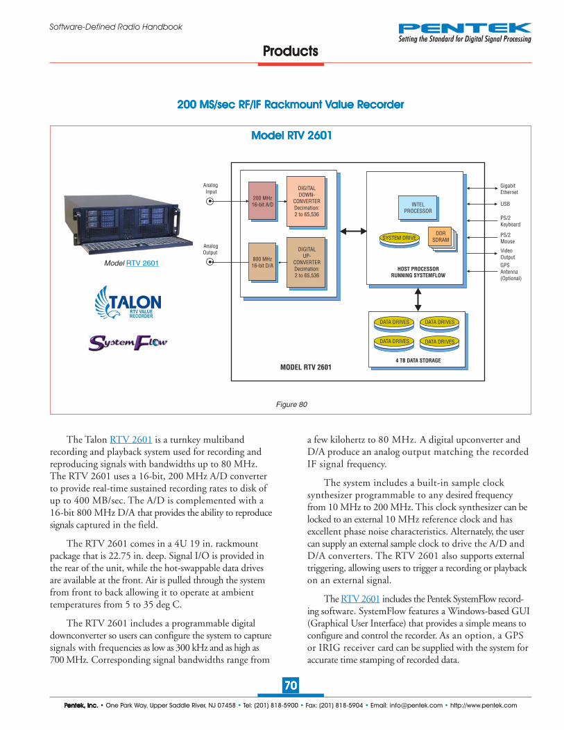
PPPPPentek, Inc.entek, Inc.entek, Inc.entek, Inc.entek, Inc. • One Park Way, Upper Saddle River, NJ 07458 • Tel: (201) 818-5900 • Fax: (201) 818-5904 • Email: [email protected] • http://www.pentek.com
7070707070
Software-Defined Radio Handbook
AnalogInput
AnalogOutput
200 MHz16-bit A/D
DIGITALDOWN-
CONVERTERDecimation:2 to 65,536
INTELPROCESSOR
SYSTEM DRIVEDDR
SDRAM
HOST PROCESSOR
RUNNING SYSTEMFLOW
4 TB DATA STORAGE
DATA DRIVES DATA DRIVES
DATA DRIVES DATA DRIVES
MODEL RTV 2601
USB
GigabitEthernet
PS/2Keyboard
PS/2Mouse
VideoOutput
GPSAntenna(Optional)
800 MHz16-bit D/A
DIGITALUP-
CONVERTERDecimation:2 to 65,536
PPPPProductsroductsroductsroductsroducts
Figure 80
Model RTV 2601 Model RTV 2601 Model RTV 2601 Model RTV 2601 Model RTV 2601
200 MS/sec RF/IF R200 MS/sec RF/IF R200 MS/sec RF/IF R200 MS/sec RF/IF R200 MS/sec RF/IF Rackmount Vackmount Vackmount Vackmount Vackmount Value Ralue Ralue Ralue Ralue Recorderecorderecorderecorderecorder
The Talon RTV 2601 is a turnkey multibandrecording and playback system used for recording andreproducing signals with bandwidths up to 80 MHz.The RTV 2601 uses a 16-bit, 200 MHz A/D converterto provide real-time sustained recording rates to disk ofup to 400 MB/sec. The A/D is complemented with a16-bit 800 MHz D/A that provides the ability to reproducesignals captured in the field.
The RTV 2601 comes in a 4U 19 in. rackmountpackage that is 22.75 in. deep. Signal I/O is provided inthe rear of the unit, while the hot-swappable data drivesare available at the front. Air is pulled through the systemfrom front to back allowing it to operate at ambienttemperatures from 5 to 35 deg C.
The RTV 2601 includes a programmable digitaldownconverter so users can configure the system to capturesignals with frequencies as low as 300 kHz and as high as700 MHz. Corresponding signal bandwidths range from
a few kilohertz to 80 MHz. A digital upconverter andD/A produce an analog output matching the recordedIF signal frequency.
The system includes a built-in sample clocksynthesizer programmable to any desired frequencyfrom 10 MHz to 200 MHz. This clock synthesizer can belocked to an external 10 MHz reference clock and hasexcellent phase noise characteristics. Alternately, the usercan supply an external sample clock to drive the A/D andD/A converters. The RTV 2601 also supports externaltriggering, allowing users to trigger a recording or playbackon an external signal.
The RTV 2601 includes the Pentek SystemFlow record-ing software. SystemFlow features a Windows-based GUI(Graphical User Interface) that provides a simple means toconfigure and control the recorder. As an option, a GPSor IRIG receiver card can be supplied with the system foraccurate time stamping of recorded data.
Model RTV 2601

PPPPPentek, Inc.entek, Inc.entek, Inc.entek, Inc.entek, Inc. • One Park Way, Upper Saddle River, NJ 07458 • Tel: (201) 818-5900 • Fax: (201) 818-5904 • Email: [email protected] • http://www.pentek.com
7171717171
Software-Defined Radio Handbook
PPPPProductsroductsroductsroductsroducts
Figure 81
Model RTV 2602 Model RTV 2602 Model RTV 2602 Model RTV 2602 Model RTV 2602
Serial FPDP RSerial FPDP RSerial FPDP RSerial FPDP RSerial FPDP Rackmount Vackmount Vackmount Vackmount Vackmount Value Ralue Ralue Ralue Ralue Recorderecorderecorderecorderecorder
Model RTV 2602
INTELPROCESSOR
SYSTEM DRIVEDDR
SDRAM
HOST PROCESSOR
RUNNING SYSTEMFLOW
4 TB DATA STORAGE
DATA DRIVES DATA DRIVES
DATA DRIVES DATA DRIVES
MODEL RTV 2602
USB
GigabitEthernet
Keyboard
Mouse
VideoOutput
GPSAntenna(Optional)
ChannelsIn / Out Serial
FPDP
The Talon RTV 2602 Serial FPDP Value Recorder isdesigned to provide a low-cost solution to users looking tocapture and play back multiple Serial FPDP streams. Itcan record up to four Serial FPDP channels to the built-in 4 TB RAID consisting of cost-effective, enterprise-classHDD storage. It is a complete turnkey recording system,ideal for capturing any type of streaming sources. Theseinclude live transfers from sensors or data from othercomputers and is fully compatible with the VITA 17.1specification.
The RTV 2602 comes in a 4U 19 in. rack-mountpackage that is 22.75 in. deep. Signal I/O is provided inthe rear of the unit, while the hot-swappable data drivesare available in the front. Air is pulled through the systemfrom front to back to allow operation at ambienttemperatures from 5o to 35o C.
The RTV 2606 can be populated with up to four SFPconnectors supporting Serial FPDP over copper, single-
mode, or multi-mode fiber, to accommodate all popularSerial FPDP interfaces. It is capable of both receiving andtransmitting data over these links and supports real-timedata storage to disk.
Programmable modes include flow control in bothreceive and transmit directions, CRC support, and copy/loop modes. The system is capable of handling 1.0625,2.125, 2.5, 3.125 and 4.25 GBaud link rates. Up to fourchannels can be recorded simultaneously with an aggregaterecording rate of up to 400 MB/sec.
As an option, a GPS or IRIG receiver card can besupplied with the system providing accurate time stampingof recorded data. Additionally, the GPS receiver deliversGPS position information that can be recorded along withthe input signals.
The RTV 2602 includes the Pentek SystemFlowrecording software which features a Windows-based GUI.

PPPPPentek, Inc.entek, Inc.entek, Inc.entek, Inc.entek, Inc. • One Park Way, Upper Saddle River, NJ 07458 • Tel: (201) 818-5900 • Fax: (201) 818-5904 • Email: [email protected] • http://www.pentek.com
7272727272
Software-Defined Radio Handbook
USB
GigabitEthernet
Aux VideoVGA Output
MODEL RTR 2726
ChannelsIn
ChannelsOut
200 MHz16-bit A/D
DIGITAL DOWNCONVERTERDEC: 2 to 64K
800 MHz16-bit D/A
DIGITAL UPCONVERTER
INT: 2 to 512K
INTELPROCESSOR
SYSTEM DRIVEDDR
SDRAM
HOST PROCESSOR
RUNNING SYSTEMFLOW
HIGH RESOLUTIONVIDEO DISPLAY
RAID DATA STORAGE
DATA DRIVES DATA DRIVES
DATA DRIVES DATA DRIVES
PPPPProductsroductsroductsroductsroducts
Model RTR 2726A RModel RTR 2726A RModel RTR 2726A RModel RTR 2726A RModel RTR 2726A Rugged Pugged Pugged Pugged Pugged Pororororortabletabletabletabletable ● ● ● ● ● Model RTS 2706 RModel RTS 2706 RModel RTS 2706 RModel RTS 2706 RModel RTS 2706 Rackmount Lackmount Lackmount Lackmount Lackmount Lab ab ab ab ab ● ● ● ● ● Model RTR 2746 RModel RTR 2746 RModel RTR 2746 RModel RTR 2746 RModel RTR 2746 RuggeduggeduggeduggeduggedRRRRRackmount ackmount ackmount ackmount ackmount ●●●●● Model RTX 2766 Extreme R Model RTX 2766 Extreme R Model RTX 2766 Extreme R Model RTX 2766 Extreme R Model RTX 2766 Extreme Rackmount ackmount ackmount ackmount ackmount ● ● ● ● ● Model RTX 2786 ½ AModel RTX 2786 ½ AModel RTX 2786 ½ AModel RTX 2786 ½ AModel RTX 2786 ½ ATRTRTRTRTR
Figure 82
The Talon RTR 2726A is a turnkey, multiband recordingand playback system that allows the user to record andreproduce high-bandwidth signals with lightweight, portableand rugged packages. This model provides aggregaterecording rates of up to 3.2 GB/sec and is ideal for theuser who requires both portability and solid perfor-mance in a compact recording system.
The RTR 2726A is supplied in a small footprint portablepackage measuring only 16.0" W x 6.9" D x 13.0" Hand weighing just less than 30 pounds.
With measurements similar to small briefcases, thisportable workstation includes Intel Core i7 processors,high-resolution 17" LCD monitors, and up to 15.3 TBof SSD storage.
A/D sampling rate, DDC decimation and bandwidth,D/A sampling rate and DUC interpolation are among
the GUI-selectable system parameters, that provide fully-programmable systems capable of recording and reproducinga wide range of signals.
Included with this system is Pentek’s SystemFlowrecording software. Built on a Windows 7 Professionalworkstation with high performance Intel Core i7 processor, thesystem allows the user to install post-processing andanalysis tools to operate on the recorded data. Theyrecord data to the native NTFS file system, providingimmediate access to the data. Custom configurationscan be stored as profiles and later loaded when needed,so users can select preconfigured settings with a single click.
Versions of the RTR 2726A are also available as aRackmount Lab unit (Model RTS 2706), Rugged Rackmount(Model RTR 2746), Extreme Rackmount (ModelRTX 2766) and Extreme ½ ATR (Model RTX 2786)
200 MS/sec RF/IF 200 MS/sec RF/IF 200 MS/sec RF/IF 200 MS/sec RF/IF 200 MS/sec RF/IF RRRRRugged Pugged Pugged Pugged Pugged Pororororortable table table table table RRRRRecorderecorderecorderecorderecorder
Model RTR 2726A

PPPPPentek, Inc.entek, Inc.entek, Inc.entek, Inc.entek, Inc. • One Park Way, Upper Saddle River, NJ 07458 • Tel: (201) 818-5900 • Fax: (201) 818-5904 • Email: [email protected] • http://www.pentek.com
7373737373
Software-Defined Radio Handbook
Figure 83
PPPPProductsroductsroductsroductsroducts
Model RTS 2707 RModel RTS 2707 RModel RTS 2707 RModel RTS 2707 RModel RTS 2707 Rackmount Lackmount Lackmount Lackmount Lackmount Lab ab ab ab ab ● ● ● ● ● Model RTR 2727 RModel RTR 2727 RModel RTR 2727 RModel RTR 2727 RModel RTR 2727 Rugged Pugged Pugged Pugged Pugged PororororortabletabletabletabletableModel RTR 2747 RModel RTR 2747 RModel RTR 2747 RModel RTR 2747 RModel RTR 2747 Rugged Rugged Rugged Rugged Rugged Rackmount ackmount ackmount ackmount ackmount ●●●●● Model RTX 2767 Extreme R Model RTX 2767 Extreme R Model RTX 2767 Extreme R Model RTX 2767 Extreme R Model RTX 2767 Extreme Rackmountackmountackmountackmountackmount
500 MS/sec RF/IF R500 MS/sec RF/IF R500 MS/sec RF/IF R500 MS/sec RF/IF R500 MS/sec RF/IF Rackmount Lackmount Lackmount Lackmount Lackmount Lab Rab Rab Rab Rab Recorderecorderecorderecorderecorder
The Talon RTS 2707 is a turnkey, multiband record-ing and playback system for recording and reproducinghigh-bandwidth signals. The RTS 2707 uses 12-bit,500 MHz A/D converters and provides agregate recordingrates up to 1.6 GB/sec.
The RTS 2707 uses Pentek’s high-powered Virtex-6-based Cobalt modules, that provide flexibility in channelcount, with optional digital downconversion capabilities.Optional 16-bit, 800 MHz D/A converters with digitalupconversion allow real-time reproduction of recordedsignals.
A/D sampling rates, DDC decimations and band-widths, D/A sampling rates and DUC interpolations areamong the GUI-selectable system parameters, providinga fully-programmable system capable of recording andreproducing a wide range of signals. Optional GPS timeand position stamping allows the user to record thiscritical signal information.
The RTS 2707 includes the SystemFlow RecordingSoftware. SystemFlow features a Windows-based GUIthat provides a simple means to configure and control therecorder.
The RTS 2707 is configured in a 4U 19" rack-mountable chassis, with hot-swappable data drives, frontpanel USB ports and I/O connectors on the rear panel.Systems are scalable to accommodate multiple chassis toincrease channel counts and aggregate data rates.
Multiple RAID levels, including 0, 1, 5, 6, 10 and50, provide a choice for the required level of redundancy.The hot-swappable HDDs provide storage capacities ofup to 100 TB in a single 6U chassis.
Versions of the RTS 2707 are available as RuggedPortable (Model RTR 2727), Rugged Rackmount (ModelRTR 2747), and Extreme Rackmount (Model RTX 2767).
Model RTS 2707
INTELPROCESSOR
SYSTEM DRIVEDDR
SDRAM
HOST PROCESSOR
RUNNING SYSTEMFLOW
RAID DATA STORE
DATA DRIVES DATA DRIVES
DATA DRIVES DATA DRIVES
MODEL RTS 2707
USB 2.0
GigabitEthernet
PS/2Keyboard
PS/2Mouse
VideoOutput
GPSAntenna(Optional)
ChannelsIn
ChannelsOut
DIGITAL DOWN-CONVERTERDEC: 2 to 64K
800 MHz16-bit D/A
Up to 4Channels
500 MHz12-bit A/D
or400 MHz14-bit A/D
Up to 4Channels
DIGITAL UP-CONVERTERINT: 2 to 64K

PPPPPentek, Inc.entek, Inc.entek, Inc.entek, Inc.entek, Inc. • One Park Way, Upper Saddle River, NJ 07458 • Tel: (201) 818-5900 • Fax: (201) 818-5904 • Email: [email protected] • http://www.pentek.com
7474747474
Software-Defined Radio Handbook
Figure 84
PPPPProductsroductsroductsroductsroducts
Model RTR 2748 R Model RTR 2748 R Model RTR 2748 R Model RTR 2748 R Model RTR 2748 Rugged Rugged Rugged Rugged Rugged Rackmount ackmount ackmount ackmount ackmount ●●●●● Model RTR 2728 RModel RTR 2728 RModel RTR 2728 RModel RTR 2728 RModel RTR 2728 Rugged Pugged Pugged Pugged Pugged PororororortabletabletabletabletableModel RTX 2768 Extreme RModel RTX 2768 Extreme RModel RTX 2768 Extreme RModel RTX 2768 Extreme RModel RTX 2768 Extreme Rackmountackmountackmountackmountackmount
1 GS/sec RF/IF R1 GS/sec RF/IF R1 GS/sec RF/IF R1 GS/sec RF/IF R1 GS/sec RF/IF Rugged Rugged Rugged Rugged Rugged Rackmount Rackmount Rackmount Rackmount Rackmount Recorderecorderecorderecorderecorder
MODEL RTR 2748
USB
GigabitEthernet
Keyboard
Mouse
VideoOutput
GPSAntenna(Optional)
ChannelIn
ChannelOut
1 GHz16-bitD/A
1 GHz12-bitA/D
ChannelIn
ChannelOut
1 GHz16-bitD/A
1 GHz12-bitA/D
(Optional)
INTELPROCESSOR
SYSTEM DRIVEDDR
SDRAM
HOST PROCESSOR
RUNNING SYSTEMFLOW
RAID DATA STORAGE
DATA DRIVES DATA DRIVES
DATA DRIVES DATA DRIVES
Model RTR 2748
The Talon RTR 2748 is a turnkey recording and playbacksystem that allows users to record and reproduce signalswith bandwidths up to 500 MHz. The RTR 2748 can beconfigured as a one- or two-channel system to providereal-time aggregate recording and playback rates up to4.0 GB/sec to an array of solid-state drives.
The RTR 2748 uses Pentek’s high-powered Virtex-6-based Cobalt boards that provide the data streamingengine for the high-speed A/D converters. A built-insynchronization module is provided to allow for multi-channel phase-coherent operation. GPS time and positionstamping is optionally available.
The RTR 2748 includes the SystemFlow RecordingSoftware. SystemFlow features a Windows-based GUIthat provides a simple means to configure and controlthe system. Custom configurations can be stored as profilesand later loaded when needed, allowing the user to selectpreconfigured settings with a single click.
Built on a Windows 7 Professional workstation,the RTR 2748 allows the user to install post-processingand analysis tools to operate on the recorded data. TheRTR 2748 records data to the native NTFS file systemthat provides immediate access to the recorded data.
Data can be off-loaded via gigabit Ethernet ports, orUSB 2.0 and USB 3.0 ports. Additionally, data can becopied to optical disk, using the 8X double layerDVD±R/RW drive.
Because SSDs operate reliably under conditions of shockand vibration, the RTR 2748 performs well in ground, ship-borne and airborne environments. The drives can be easilyremoved or exchanged during a mission to retrieve the data.
Versions of the RTR 2748 are also available as aRugged Portable (Model RTR 2728), and ExtremeRackmount (Model RTX 2768).
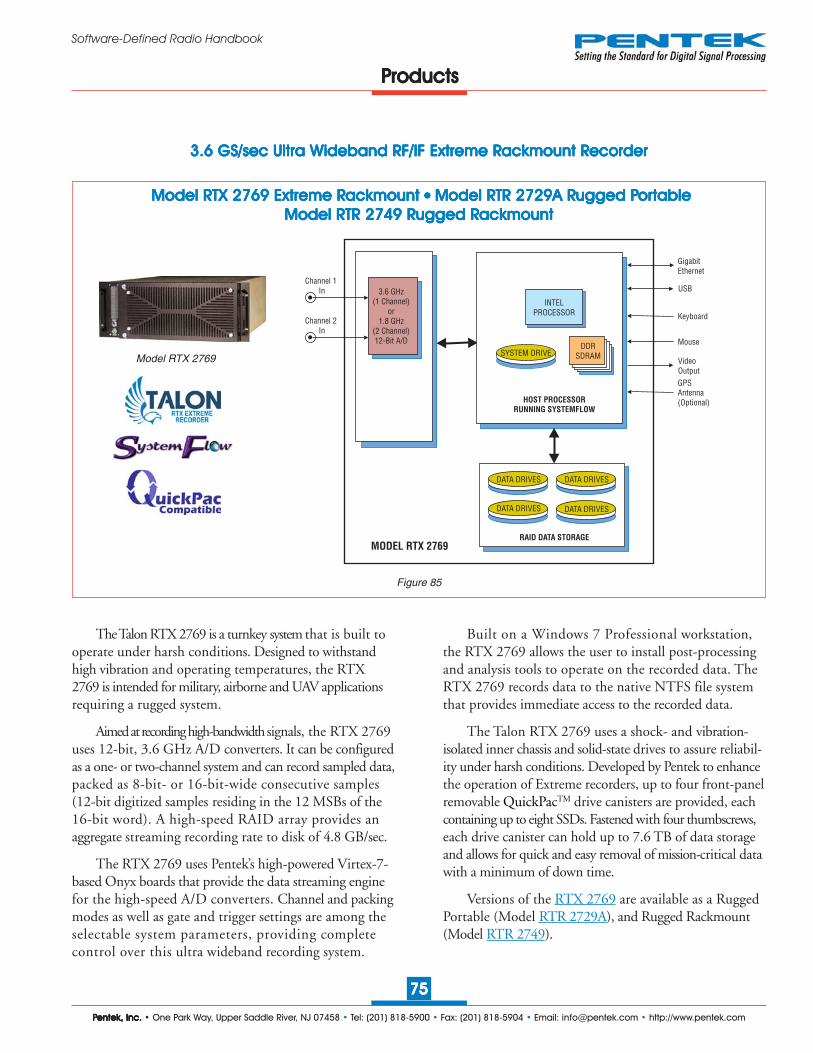
PPPPPentek, Inc.entek, Inc.entek, Inc.entek, Inc.entek, Inc. • One Park Way, Upper Saddle River, NJ 07458 • Tel: (201) 818-5900 • Fax: (201) 818-5904 • Email: [email protected] • http://www.pentek.com
7575757575
Software-Defined Radio Handbook
Figure 85
PPPPProductsroductsroductsroductsroducts
Model RTX 2769 Extreme R Model RTX 2769 Extreme R Model RTX 2769 Extreme R Model RTX 2769 Extreme R Model RTX 2769 Extreme Rackmount ackmount ackmount ackmount ackmount ●●●●● Model RTR 2729A RModel RTR 2729A RModel RTR 2729A RModel RTR 2729A RModel RTR 2729A Rugged Pugged Pugged Pugged Pugged PororororortabletabletabletabletableModel RTR 2749 RModel RTR 2749 RModel RTR 2749 RModel RTR 2749 RModel RTR 2749 Rugged Rugged Rugged Rugged Rugged Rackmountackmountackmountackmountackmount
Channel 1In 3.6 GHz
(1 Channel)or
1.8 GHz(2 Channel)12-Bit A/D
MODEL RTX 2769
Keyboard
Mouse
VideoOutput
GPSAntenna(Optional)
Channel 2In
USB
GigabitEthernet
INTELPROCESSOR
SYSTEM DRIVEDDR
SDRAM
HOST PROCESSOR
RUNNING SYSTEMFLOW
RAID DATA STORAGE
DATA DRIVES DATA DRIVES
DATA DRIVES DATA DRIVES
Model RTX 2769
3.6 GS/sec Ultra W3.6 GS/sec Ultra W3.6 GS/sec Ultra W3.6 GS/sec Ultra W3.6 GS/sec Ultra Wideband RF/IF Extreme Rideband RF/IF Extreme Rideband RF/IF Extreme Rideband RF/IF Extreme Rideband RF/IF Extreme Rackmount Rackmount Rackmount Rackmount Rackmount Recorderecorderecorderecorderecorder
The Talon RTX 2769 is a turnkey system that is built tooperate under harsh conditions. Designed to withstandhigh vibration and operating temperatures, the RTX2769 is intended for military, airborne and UAV applicationsrequiring a rugged system.
Aimed at recording high-bandwidth signals, the RTX 2769uses 12-bit, 3.6 GHz A/D converters. It can be configuredas a one- or two-channel system and can record sampled data,packed as 8-bit- or 16-bit-wide consecutive samples(12-bit digitized samples residing in the 12 MSBs of the16-bit word). A high-speed RAID array provides anaggregate streaming recording rate to disk of 4.8 GB/sec.
The RTX 2769 uses Pentek’s high-powered Virtex-7-based Onyx boards that provide the data streaming enginefor the high-speed A/D converters. Channel and packingmodes as well as gate and trigger settings are among theselectable system parameters, providing completecontrol over this ultra wideband recording system.
Built on a Windows 7 Professional workstation,the RTX 2769 allows the user to install post-processingand analysis tools to operate on the recorded data. TheRTX 2769 records data to the native NTFS file systemthat provides immediate access to the recorded data.
The Talon RTX 2769 uses a shock- and vibration-isolated inner chassis and solid-state drives to assure reliabil-ity under harsh conditions. Developed by Pentek to enhancethe operation of Extreme recorders, up to four front-panelremovable QuickPacTM drive canisters are provided, eachcontaining up to eight SSDs. Fastened with four thumbscrews,each drive canister can hold up to 7.6 TB of data storageand allows for quick and easy removal of mission-critical datawith a minimum of down time.
Versions of the RTX 2769 are available as a RuggedPortable (Model RTR 2729A), and Rugged Rackmount(Model RTR 2749).
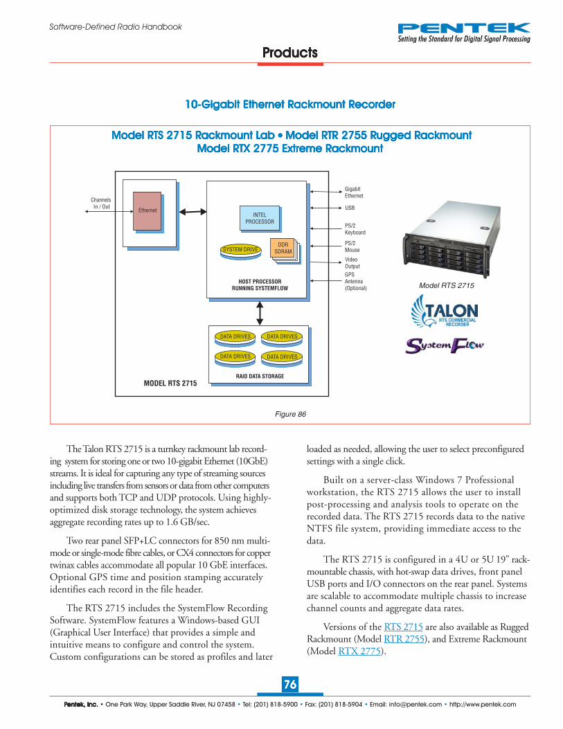
PPPPPentek, Inc.entek, Inc.entek, Inc.entek, Inc.entek, Inc. • One Park Way, Upper Saddle River, NJ 07458 • Tel: (201) 818-5900 • Fax: (201) 818-5904 • Email: [email protected] • http://www.pentek.com
7676767676
Software-Defined Radio Handbook
PPPPProductsroductsroductsroductsroducts
Model RTS 2715 R Model RTS 2715 R Model RTS 2715 R Model RTS 2715 R Model RTS 2715 Rackmount Lackmount Lackmount Lackmount Lackmount Lab ab ab ab ab ●●●●● Model RTR 2755 R Model RTR 2755 R Model RTR 2755 R Model RTR 2755 R Model RTR 2755 Rugged Rugged Rugged Rugged Rugged RackmountackmountackmountackmountackmountModel RTX 2775 Extreme RModel RTX 2775 Extreme RModel RTX 2775 Extreme RModel RTX 2775 Extreme RModel RTX 2775 Extreme Rackmountackmountackmountackmountackmount
Figure 86
10-10-10-10-10-Gigabit Ethernet RGigabit Ethernet RGigabit Ethernet RGigabit Ethernet RGigabit Ethernet Rackmount Rackmount Rackmount Rackmount Rackmount Recorderecorderecorderecorderecorder
ChannelsIn / Out
Ethernet
MODEL RTS 2715
USB
GigabitEthernet
PS/2Keyboard
PS/2Mouse
VideoOutput
GPSAntenna(Optional)
INTELPROCESSOR
SYSTEM DRIVEDDR
SDRAM
HOST PROCESSOR
RUNNING SYSTEMFLOW
RAID DATA STORAGE
DATA DRIVES DATA DRIVES
DATA DRIVES DATA DRIVES
The Talon RTS 2715 is a turnkey rackmount lab record-ing system for storing one or two 10-gigabit Ethernet (10GbE)streams. It is ideal for capturing any type of streaming sourcesincluding live transfers from sensors or data from other computersand supports both TCP and UDP protocols. Using highly-optimized disk storage technology, the system achievesaggregate recording rates up to 1.6 GB/sec.
Two rear panel SFP+LC connectors for 850 nm multi-mode or single-mode fibre cables, or CX4 connectors for coppertwinax cables accommodate all popular 10 GbE interfaces.Optional GPS time and position stamping accuratelyidentifies each record in the file header.
The RTS 2715 includes the SystemFlow RecordingSoftware. SystemFlow features a Windows-based GUI(Graphical User Interface) that provides a simple andintuitive means to configure and control the system.Custom configurations can be stored as profiles and later
loaded as needed, allowing the user to select preconfiguredsettings with a single click.
Built on a server-class Windows 7 Professionalworkstation, the RTS 2715 allows the user to installpost-processing and analysis tools to operate on therecorded data. The RTS 2715 records data to the nativeNTFS file system, providing immediate access to thedata.
The RTS 2715 is configured in a 4U or 5U 19" rack-mountable chassis, with hot-swap data drives, front panelUSB ports and I/O connectors on the rear panel. Systemsare scalable to accommodate multiple chassis to increasechannel counts and aggregate data rates.
Versions of the RTS 2715 are also available as RuggedRackmount (Model RTR 2755), and Extreme Rackmount(Model RTX 2775).
Model RTS 2715

PPPPPentek, Inc.entek, Inc.entek, Inc.entek, Inc.entek, Inc. • One Park Way, Upper Saddle River, NJ 07458 • Tel: (201) 818-5900 • Fax: (201) 818-5904 • Email: [email protected] • http://www.pentek.com
7777777777
Software-Defined Radio Handbook
Figure 87
TTTTTalon Ralon Ralon Ralon Ralon Recordersecordersecordersecordersecorders
Serial FPDP RSerial FPDP RSerial FPDP RSerial FPDP RSerial FPDP Rugged Pugged Pugged Pugged Pugged Pororororortable Rtable Rtable Rtable Rtable Recorderecorderecorderecorderecorder
Model RTR 2736A R Model RTR 2736A R Model RTR 2736A R Model RTR 2736A R Model RTR 2736A Rugged Pugged Pugged Pugged Pugged Pororororortable table table table table ●●●●● Model RTS 2716 R Model RTS 2716 R Model RTS 2716 R Model RTS 2716 R Model RTS 2716 Rackmount Lackmount Lackmount Lackmount Lackmount LabababababModel RTR 2756 RModel RTR 2756 RModel RTR 2756 RModel RTR 2756 RModel RTR 2756 Rugged Rugged Rugged Rugged Rugged Rackmount ackmount ackmount ackmount ackmount ● ● ● ● ● Model RTX 2776 Extreme RModel RTX 2776 Extreme RModel RTX 2776 Extreme RModel RTX 2776 Extreme RModel RTX 2776 Extreme Rackmountackmountackmountackmountackmount
RAID DATA STORAGE
DATA DRIVES DATA DRIVES
DATA DRIVES DATA DRIVES
MODEL RTR 2736
USB
GigabitEthernet
PS/2Keyboard
PS/2Mouse
VideoOutput
GPSAntenna(Optional)
ChannelsIn / Out Serial
FPDP
INTELPROCESSOR
SYSTEM DRIVEDDR
SDRAM
HOST PROCESSOR
RUNNING SYSTEMFLOW
The Talon RTR 2736A is a complete turnkey record-ing system designed to operate under conditions of shockand vibration. It records and plays back multiple serialFPDP data streams in a rugged, lightweight portablepackage. It is ideal for capturing any type of streamingsources including live transfers from sensors or data fromother computers and is fully compatible with the VITA17.1 specification. Using highly-optimized disk storagetechnology, this system achieves aggregate recording ratesup to 3.2 GB/sec.
The system can be populated with up to eight SFPconnectors supporting Serial FPDP over copper, single-mode,or multi-mode fiber, to accommodate all popular serial FPDPinterfaces. It is capable of receiving and transmitting dataover these links and supports real-time data storage to disk.The system is capable of handling 1.0625, 2.125, 2.5,3.125 and 4.25 GBaud link rates supporting data transferrates of up to 420 MB/sec per serial FPDP link.
The system includes the SystemFlow RecordingSoftware. SystemFlow features a Windows-based GUIthat provides a simple and intuitive means to configureand control the system. Custom configurations can bestored as profiles and later loaded as needed, allowing theuser to select preconfigured settings with a single click.
The RTR 2736A is configured in portable, lightweightchassis with hot-swap SSDs, front panel USB ports andI/O connections on the side panel. It is built in extremelyrugged, 100% aluminum alloy unit, reinforced with shockabsorbing rubber corners and impact-resistant protectiveglass. Using vibration- and shock-resistant SSDs, thesystem is designed to operate reliably as a portable fieldsystem in harsh environments.
Versions of the RTR 2736A are also available as aRackmount Lab unit (Model RTS 2716), RuggedRackmount (Model RTR 2756), and Extreme Rackmount(Model RTX 2776).
Model RTR 2736A

PPPPPentek, Inc.entek, Inc.entek, Inc.entek, Inc.entek, Inc. • One Park Way, Upper Saddle River, NJ 07458 • Tel: (201) 818-5900 • Fax: (201) 818-5904 • Email: [email protected] • http://www.pentek.com
7878787878
Software-Defined Radio Handbook
Figure 88
PPPPProductsroductsroductsroductsroducts
LLLLLVDS Digital I/O Extreme RVDS Digital I/O Extreme RVDS Digital I/O Extreme RVDS Digital I/O Extreme RVDS Digital I/O Extreme Rackmount Rackmount Rackmount Rackmount Rackmount Recorderecorderecorderecorderecorder
Model RTX 2778 Extreme R Model RTX 2778 Extreme R Model RTX 2778 Extreme R Model RTX 2778 Extreme R Model RTX 2778 Extreme Rackmount ackmount ackmount ackmount ackmount ● ● ● ● ● Model RTS 2718 RModel RTS 2718 RModel RTS 2718 RModel RTS 2718 RModel RTS 2718 Rackmount Lackmount Lackmount Lackmount Lackmount LabababababModel RTR 2738 RModel RTR 2738 RModel RTR 2738 RModel RTR 2738 RModel RTR 2738 Rugged Pugged Pugged Pugged Pugged Pororororortable table table table table ● ● ● ● ● Model RTR 2758 RModel RTR 2758 RModel RTR 2758 RModel RTR 2758 RModel RTR 2758 Rugged Rugged Rugged Rugged Rugged Rackmountackmountackmountackmountackmount
Model RTX 2778
32-bitData In
32-bitLVDS I/ORecord
Interface
MODEL RTX 2778
Keyboard
Mouse
VideoOutput
GPSAntenna(Optional)
Clock
Data Valid
Data Suspend
32-bitData Out Optional
32-bitLVDS I/OPlaybackInterface
Clock
Data Valid
Data Suspend
USB
GigabitEthernet
INTELPROCESSOR
SYSTEM DRIVEDDR
SDRAM
HOST PROCESSOR
RUNNING SYSTEMFLOW
RAID DATA STORAGE
DATA DRIVES DATA DRIVES
DATA DRIVES DATA DRIVES
The Talon RTX 2778 is a turnkey record and playbacksystem that is built to operate under harsh conditions.Designed to withstand high vibration and operating tempera-tures, the RTX 2778 is intended for military, airborneand UAV applications requiring a rugged system.
The RTX 2778 records and plays back digital datausing the Pentek Model 78610 LVDS digital I/O board.Using highly optimized disk storage technology, the systemachieves aggregate recording rates of up to 1.0 GB/sec.
The RTX 2778 utilizes a 32-bit LVDS interfacethat can be clocked at speeds up to 250 MHz. It includesData Valid and Suspend signals and provides the abilityto turn these signals on and off as well as control their polarity.
The RTX 2778 includes the SystemFlow Record-ing Software. SystemFlow features a Windows-basedGUI (Graphical User Interface) that provides a simplemeans to configure and control the system.
Built on a Windows 7 Professional workstation,the RTX 2778 allows the user to install post-processingand analysis tools to operate on the recorded data. TheRTX 2778 records data to the native NTFS file system,providing immediate access to the recorded data.
The Talon RTX 2778 uses a shock- and vibration-isolated inner chassis and solid-state drives to assure reliabil-ity under harsh conditions. Developed by Pentek to enhancethe operation of Extreme recorders, up to four front-panelremovable QuickPacTM drive canisters are provided, eachcontaining up to eight SSDs. Fastened with four thumbscrews,each drive canister can hold up to 7.6 TB of data storageand allows for quick and easy removal of mission-critical datawith a minimum of down time.
Versions of the RTX 2778 are also available as aRackmount Lab unit (Model RTS 2718), RuggedPortable (Model RTR 2738), and Rugged Rackmount(Model RTR 2758).

PPPPPentek, Inc.entek, Inc.entek, Inc.entek, Inc.entek, Inc. • One Park Way, Upper Saddle River, NJ 07458 • Tel: (201) 818-5900 • Fax: (201) 818-5904 • Email: [email protected] • http://www.pentek.com
7979797979
Software-Defined Radio Handbook
ApplicationsApplicationsApplicationsApplicationsApplications
Figure 89
INTELPROCESSOR
SYSTEM DRIVEDDR
SDRAM
HOST PROCESSOR
UP TO 20 TB RAID
DATA DRIVES DATA DRIVES
DATA DRIVES DATA DRIVES
USB 2.0
GigabitEthernet
PS/2Keyboard
PS/2Mouse
VideoOutput
2
6
eSATA2
GPSAntenna
x8 PCIe
x8 PCIe
Input A
Input B
Input C
Input D
200 MHzA/D
200 MHzA/D
200 MHzA/D
200 MHzA/D
FPGAwith
4 banks of8-Channel
DDC
Pentek Cobalt 78622 PCIe Board
Input A
Input B
Input C
Input D
200 MHzA/D
200 MHzA/D
200 MHzA/D
200 MHzA/D
FPGAwith
4 banks of8-Channel
DDC
Pentek Cobalt 78622 PCIe Board
64-64-64-64-64-Channel SofChannel SofChannel SofChannel SofChannel Software Rtware Rtware Rtware Rtware Radio Radio Radio Radio Radio Recording Systemecording Systemecording Systemecording Systemecording System
Each DDC delivers a complex output stream consist-ing of 24-bit I + 24-bit Q samples at a rate of ƒs/N. Anynumber of channels can be enabled within each bank,selectable from 0 to 8. Each bank includes an outputsample interleaver that delivers a channel-multiplexedstream for all enabled channels within a bank.
An internal timing bus provides all timing and synchro-nization required by the eight A/D converters. It includesa clock, two sync and two gate or trigger signals. An on-board clock generator receives an external sample clock.This clock can be used directly by the A/D or divided bya built-in clock synthesizer circuit.
Built on a Windows 7 Professional workstation withhigh performance Intel Core i7 processor this systemallows the user to install post processing and analysistools to operate on the recorded data. The system recordsdata to the native NTFS file system, providing immediateaccess to the recorded data.
Included with this system is Pentek’s SystemFlowrecording software. Optional GPS time and positionstamping allows the user to record this critical signalinformation.
Shown above is a 64-channel recording system utilizingtwo Pentek Cobalt 78662 PCIe boards. The 78662samples four input channels at up to 200 megasamplesper second, thereby accommodating input signals withup to 80 MHz bandwidth.
Factory-installed in the FPGA of each 78662 is apowerful DDC IP core containing 32 channels. Each ofthe 32 channels has an independent 32-bit tuningfrequency setting that ranges from DC to ƒs, where ƒs isthe A/D sampling frequency. All of the eight channelswithin each bank share a common decimation settingthat can range from 16 to 8192. For example, with asampling rate of 200 MHz, the available output band-widths range from 19.53 kHz to 10.0 MHz. Each 8-channelbank can have its own unique decimation setting support-ing a different bandwidth associated with each of the fouracquisition modules.
The decimating filter for each DDC bank acceptsa unique set of user-supplied 18-bit coefficients. The 80%default filters deliver an output bandwidth of 0.8*ƒs/N,where N is the decimation setting. The rejection ofadjacent-band components within the 80% outputbandwidth is better than 100 dB.

PPPPPentek, Inc.entek, Inc.entek, Inc.entek, Inc.entek, Inc. • One Park Way, Upper Saddle River, NJ 07458 • Tel: (201) 818-5900 • Fax: (201) 818-5904 • Email: [email protected] • http://www.pentek.com
8080808080
Software-Defined Radio Handbook
LLLLL-Band Signal P-Band Signal P-Band Signal P-Band Signal P-Band Signal Processing Systemrocessing Systemrocessing Systemrocessing Systemrocessing System
ApplicationsApplicationsApplicationsApplicationsApplications
The Cobalt Model 78690 L-Band RF Tuner targetsreception and processing of digitally-modulated RFsignals such as satellite television and terrestrial wirelesscommunications. The 78690 requires only an antennaand a host computer to form a complete L-band SDRdevelopment platform.
This system receives L-Band signals between 925 MHzand 2175 MHz directly from an antenna. Signals abovethis range such as C Band, Ku Band and K band can bedownconverted to L-Band through an LNB (Low NoiseBlock) downconverter installed in the receiving antenna.
The Maxim Max2112 L-Band Tuner IC features alow-noise amplifier with programmable gain from 0 to65 dB and a synthesized local oscillator programmablefrom 925 to 2175 MHz. The complex analog mixertranslates the input signals down to DC. Basebandamplifiers provide programmable gain from 0 to 15 dBin steps of 1 dB. The bandwidth of the baseband lowpassfilters can be programmed from 4 to 40 MHz . TheMaxim IC accommodates full-scale input levels of -50 dBmto +10 dbm and delivers I and Q complex baseband outputs.
Figure 90
Analog Digital
Baseband IL-Band
x8 PCIe
LNA
Analog Local
Oscillator
Synthesizer
Q
Baseband AmpsAnalog Mixer
Analog Mixer
I
AnalogLowpass
FilterA/D
A/D
FPGA
VIRTEX-6
PC
WINDOWS
RF Input Baseband Q
MaximMAX2112
Pentek 78690 PCIe Board
LowpassFilter
Analog
The complex I and Q outputs are digitized by two200 MHz 16-bit A/D converters operating synchronously.
The Virtex-6 FPGA is a powerful resource forrecovering and processing a wide range of signalswhile supporting decryption, decoding, demodula-tion, detection, and analysis. It is ideal for interceptingor monitoring traffic in SIGINT and COMINTapplications. Other applications that benefit includemobile phones, GPS, satellite terminals, military telem-etry, digital video and audio in TV broadcasting satellites,and voice, video and data communications.
This L-Band signal processing system is ideal as afront end for government and military systems. Its smallsize adderesses space-limited applications. Ruggedizedoptions are also available from Pentek with the Models71690 XMC module and the 53690 OpenVPX board toaddress UAV applications and other severe environments.
Development support for this system is provided bythe Pentek ReadyFlow board support package for Windows,Linux and VxWorks. Also available is the Pentek GateFlowFPGA Design Kit to support custom algorithm development.

PPPPPentek, Inc.entek, Inc.entek, Inc.entek, Inc.entek, Inc. • One Park Way, Upper Saddle River, NJ 07458 • Tel: (201) 818-5900 • Fax: (201) 818-5904 • Email: [email protected] • http://www.pentek.com
8181818181
Software-Defined Radio Handbook
ApplicationsApplicationsApplicationsApplicationsApplications
Figure 91
8-8-8-8-8-Channel OpenVPX Beamforming SystemChannel OpenVPX Beamforming SystemChannel OpenVPX Beamforming SystemChannel OpenVPX Beamforming SystemChannel OpenVPX Beamforming System
Two Model 53661 boards are installed in slots 1 and2 of an OpenVPX backplane, along with a CPU boardin slot 3. Eight dipole antennas designed for receiving2.5 GHz signals feed RF Tuners containing low noiseamplifiers, local oscillators and mixers. The RF Tunerstranslate the 2.5 GHz antenna frequency signal downto an IF frequency of 50 MHz.
The 200 MHz 16-bit A/Ds digitize the IF signalsand perform further frequency downconversion to baseband,with a DDC decimation of 128. This provides I+Q complexoutput samples with a bandwidth of about 1.25 MHz. Phaseand gain coefficients for each channel are applied tosteer the array for directionality.
The CPU board in VPX slot 3 sends commandsand coefficients across the backplane over two x4 PCIelinks, or OpenVPX “fat pipes”.
The first four signal channels are processed in theupper left 53661 board in VPX slot 1, where the 4-channelbeamformed sum is propagated through the 4X AuroraSum Out link across the backplane to the 4X Aurora SumIn port on the second 53661 in slot 2. The 4-channel localsummation from the second 53661 is added to the propa-gated sum from the first board to form the complete 8-channelsum. This final sum is sent across the x4 PCIe link to theCPU card in slot 3.
Assignment of the three OpenVPX 4X links on theModel 53661 boards is simplified through the use of acrossbar switch which allows the 53661 to operate witha wide variety of different backplanes.
Because OpenVPX does not restrict the use of serialprotocols across the backplane links, mixed protocolarchitectures like the one shown are fully supported. ➤
VPX P1
Slot 1
EP02
EP01
DP01
FP C
VPX P1
Slot 2
VPX P1
Slot 3 CPU
EP02
EP01
DP01
FPC
x4 PCIe
x4 PCIe
200 MHz
16-bit A/D
DDC 4G + Phase
PCIe
x4
I/F
200 MHz16-bit A/D
200 MHz
16-bit A/D
200 MHz
16-bit A/D
AURORA
BEAMFORMSUMMATION
DDC 3
G + Phase
DDC 2G + Phase
DDC 1
G + Phase
4X Sum In
4X Sum Out
Model 53661
x4 PCIe
200 MHz
16-bit A/D
DDC 4
G + Phase
PCIe
x4
I/F
200 MHz16-bit A/D
200 MHz
16-bit A/D
200 MHz
16-bit A/D
AURORA
BEAMFORMSUMMATION
DDC 3
G + Phase
DDC 2
G + Phase
DDC 1
G + Phase
4X Sum In
4X Sum Out
x4 PCIe
Model 53661
RF Tuner
RF Tuner
RF Tuner
RF Tuner
RF Tuner
RF Tuner
RF Tuner
RF Tuner
FP B
FP A
DP01
DP02
OpenVPX
CPUBoard
VPXBACKPLANE
4X Aurora

PPPPPentek, Inc.entek, Inc.entek, Inc.entek, Inc.entek, Inc. • One Park Way, Upper Saddle River, NJ 07458 • Tel: (201) 818-5900 • Fax: (201) 818-5904 • Email: [email protected] • http://www.pentek.com
8282828282
Software-Defined Radio Handbook
ApplicationsApplicationsApplicationsApplicationsApplications
Figure 92
8-8-8-8-8-Channel OpenVPX Beamforming Demo systemChannel OpenVPX Beamforming Demo systemChannel OpenVPX Beamforming Demo systemChannel OpenVPX Beamforming Demo systemChannel OpenVPX Beamforming Demo system
➤➤➤➤➤ Beamforming Demo System
The beamforming demo system is equipped with aControl Panel that runs under Windows on the CPUboard. It includes an automatic signal scanner to detectthe strongest signal frequency arriving from a testtransmitter. This frequency is centered around the50 MHz IF frequency of the RF downconverter. Oncethe frequency is identified, the eight DDCs are setaccordingly to bring that signal down to 0 Hz forsummation.
The control panel software also allows specifichardware settings for all of the parameters for the eightchannels including gain, phase, and sync delay.
An additional display shows the beam-formed pattern ofthe array. This display is formed by adjusting the phaseshift of each of the eight channels to provide maximum
sensitivity across arrival angles from -90O to +90O
perpendicular to the plane of the array.
The classic 7-lobe pattern for an ideal 8-elementarray for a signal arriving at 0O angle (directly in front ofthe array) is shown above. Below the lobe pattern is apolar plot showing a single vector pointing to thecomputed angle of arrival. This is derived from identify-ing the lobe with the maximum response.
An actual plot of a real-life transmitter is also shownfor a source directly in front of the display. In this casethe perfect lobe pattern is affected by physical objects,reflections, cable length variations and minor differencesin the antennas. Nevertheless, the directional informationis computed quite well. As the signal source is moved leftand right in front of the array, the peak lobe moves withit, changing the computed angle of arrival.
This demo system is available online at Pentek. Ifyou are interested in viewing a live demonstration, pleaselet us know of your interest by clicking on this link:
Beamforming Demo.
Beamforming Demo Control Panel Theoretical 7-lobe Beamforming Patern Real-Life Beamforming Patern