solution guide management - xilinx - all programmable welcome to the first edition of the xilinx®...
TRANSCRIPT

Issue 1 July 2005
PowerManagementPowerManagement
Solution Guide
INSIDEARTICLES
Conquering the Three Challenges of Power Consumption
The Virtex-4 Power Play
WHITE PAPERS
Power vs. Performance: The 90 nm Inflection Point
APPLICATION NOTES
Managing Power withCoolRunner-II CPLDs
INSIDEARTICLES
Conquering the Three Challenges of Power Consumption
The Virtex-4 Power Play
WHITE PAPERS
Power vs. Performance: The 90 nm Inflection Point
APPLICATION NOTES
Managing Power withCoolRunner-II CPLDs
Solving Today's HotChallenge
Solving Today's HotChallenge
R

ARTICLES
Conquering the Three Challenges of Power Consumption .........................................5
The Virtex-4 Power Play....................................................................................8
WHITE PAPERS
Power/Performance Inflection at 90nm Technology Node...................................13
Static Power and Temperature ........................................................................29
APPLICATION NOTES
Using CoolRunner-II Advanced Features............................................................37
Low Power Design with CoolRunner-II CPLDs .....................................................47
Using DataGATE in CoolRunner-II CPLDs ..........................................................56
Managing Power with CoolRunner-II CPLDs ......................................................64
C O N T E N T S
P O W E R M A N A G E M E N T S O L U T I O N G U I D E I S S U E 1, A U G U S T 2 0 0 5
“FPGAs are being used increasingly inmany applications, so reducing powerconsumption in FPGAs provides huge
benefits to the system design.”
Learn more about power management solutions from Xilinx at: www.xilinx.com/xcell/power1/

WWelcome to the first edition of the Xilinx® Power Management Solution Guide. At Xilinx, we haveheard a clear message from our customers that power is now a key issue in many system designs.No longer an afterthought, power must now be budgeted and managed just as much as the bill ofmaterials cost or system performance. You have told us that meeting only two of these three keyparameters just isn’t good enough anymore.
With these thoughts in mind, we have assembled a collection of the most recent – and we hopeuseful – articles, white papers, and application notes dealing with system power management.
This issue includes several articles and white papers discussing the system power advantages andpower management features of the Virtex™-4 FPGA solution. Virtex-4 FPGAs dramaticallyreduce power consumption compared to other FPGAs in all three key power areas – static power,dynamic power, and in-rush or startup current. They offer as much as 73% lower static power withthe industry’s first triple-oxide technology; as much as 86% lower dynamic power enabled byembedded IP blocks; and the industry’s lowest in-rush current.
These savings are enabled with industry-leading technologies, including the industry-first 90 nmtriple-oxide technology, high-performance embedded IP, and power-saving configuration circuitry.In addition to the chip technology itself, Xilinx provides comprehensive tools for power systemdesign, including a Web-based power estimator and the post-implementation XPower tool includ-ed as part of the ISE™ design tool suite.
This issue also features a collection of application notes detailing some of the innovative power-saving features of the CoolRunner™-II CPLD. Long the industry’s benchmark for low-powerCPLDs, the CoolRunner-II family offers both power-saving technology and power-managementfeatures that make it the best choice for today’s low-power, portable systems.
We hope you find this solution guide valuable. It is, however, just a sample of the informationavailable to you about this topic. For access to all of the latest on power management, visit ourwebsite at www.xilinx.com/xcell/power1/.
Thank you,
Xilinx, Inc.2100 Logic DriveSan Jose, CA 95124-3400Phone: 408-559-7778FAX: 408-879-4780
© 2005 Xilinx, Inc. All rights reserved. XILINX, the Xilinx Logo, and otherdesignated brands includedherein are trademarks of Xilinx, Inc. PowerPC is atrademark of IBM, Inc. All other trademarks are theproperty of their respective owners.
The articles, information, and other materials included inthis issue are provided solely for the convenience of ourreaders. Xilinx makes no warranties, express, implied,statutory, or otherwise, and accepts no liability withrespect to any such articles, information, or other materials or their use, and any use thereof is solely atthe risk of the user. Any person or entity using suchinformation in any way releases and waives any claim itmight have against Xilinx for any loss, damage, orexpense caused thereby.
More Power to You
Sandeep VijVice President Worldwide Marketing
EDITOR IN CHIEF Carlis [email protected]
MANAGING EDITOR Forrest [email protected]
ASSISTANT MANAGING EDITOR Charmaine Cooper Hussain
XCELL ONLINE EDITOR Tom [email protected]
ADVERTISING SALES Dan Teie1-800-493-5551
ART DIRECTOR Scott Blair
PowerManagement
Solution Guide
by Steve SharpSr. Manager, Corporate Solutions MarketingXilinx, [email protected]
As chip technology progresses to 90 nmand below, power becomes a burningissue in system design. At this node, leak-age plays a more major role in totalpower; smaller interconnect geometrieswith new dielectric materials affectdynamic power as well.
According to Jordan Selburn of marketresearch firm iSupply, “Leakage current –essentially insignificant at the 0.35 micronnode and earlier – has become a major issueas transistors become increasingly leakier.Studies have shown that at the 90 nmnode, leakage power can equal dynamicpower consumption and even exceed it atthe 65 nm node.”
Another factor facing system designersis the tighter power budgets around
which they must design. This is not lim-ited to any single type of system, butdoes affect most designers. Large systemswith many boards or modules, as well asportable and consumer products, all facepower budgeting issues.
In large systems, power budgeting istypically done for the total system, as wellas distributed power regulation on a per-board or per-module basis. With multiplepower supplies now on every board, it isnot a simple task to increase the powerbudget for one board without affecting theentire system’s power distribution plan.
In line-powered consumer products,the goal is usually to use the smallest andleast-expensive power supply possible tokeep costs under control. Exceeding thecapabilities of a particular model powersupply by only a few percent can necessi-tate the use of a larger, more expensivesupply, and this might be unacceptable inlight of total system cost. Designers
would rather design in more features todifferentiate the product than to use alarger power supply.
In portable consumer products, theoverwhelming goal is to extend battery lifefor as long as possible. For these products,longer battery life – both in active andstandby modes – is a significant competi-tive advantage.
With all of these challenges, it’s no won-der that power issues are sounding thealarm bells for system designers today.iSuppli’s Selburn continues, “On the cus-tomer side, chip designers can considerarchitectural approaches such as parallelprocessing at reduced clock speeds toreduce dynamic power, or gated clocks thatessentially turn off entire sections of thechip when they are not needed. Despitethese techniques, power consumptionremains a serious issue for a large portion ofthe core silicon market, an issue that isbecoming worse, not better, with time.”
Conquering the Three Challenges of Power ConsumptionConquering the Three Challenges of Power Consumption
August 2005 Power Management Solution Guide 5
Why is power such an issue?Why is power such an issue?

System Design ChallengesThere are three key areas of power usage andcontrol challenging system designers today:static power, dynamic power, and in-rushpower. Each presents different issues andrequires different methods to calculate andmanage power.
Static power is the power consumed by adevice when it is in its quiescent conditionwith no input signals being exercised. It isalso referred to as steady-state or standbypower. In today’s 90 nm technology devices,leakage currents in the transistors are thebiggest contributors to static power. This isusually the key parameter of concern todesigners of portable equipment because ofits effect on battery life, especially fordevices that spend large amounts of time ina standby condition waiting for input fromthe outside world.
Dynamic power is the power consumedduring normal operation. It is also referred toas operating power. Dynamic power is depen-dant on operating signal frequency, intercon-nect capacitance, and operating voltage.Because the voltage dependency is a squarefunction, the reduction in voltage when mov-ing to 90 nm devices has substantially reducedoperating power in many devices. However,for large, high-performance systems with highoperating frequencies, dynamic power is still asignificant component of total system power.
In-rush power is the power required atdevice power-up. It is also referred to aspower-up or start-up power, or power-onsurge power (or current). Some devicesrequire many times more power to beginoperation than they do during normaloperation, thereby placing demands onsystem power supplies. In a consumer sys-tem with very tightly controlled powersupply size and cost, ensuring that in-rushpower is not more than normal operatingpower is a key design goal.
Higher power levels can affect both man-ufacturers and end-customers alike, in fourkey areas:
• Performance. Higher power levels in achip can limit device and end-systemperformance by forcing a lower systemclock rate to stay within the systempower budget.
This is enabled with industry-leadingtechnologies such as 90 nm triple-oxidetechnology, high-performance embedded IP,and power-saving configuration circuitry.
Xilinx also provides comprehensivetools for power system design: Virtex-4datasheet and user guide; a web-basedpower estimator; and XPower, included inISE™ software.
Virtex-4 devices handle the three typesof power usage and control in the follow-ing ways:
• Static power. As process geometriesshrink to 90 nm and lower, theindustry expects higher leakage andhigher static power when channellength decreases. Working with fabpartner United Microelectronics
Corp., Xilinx solved this problem byusing triple-oxide technology in theVirtex-4 90 nm process, whichreduces leakage current significantly.Two-oxide thicknesses are widely usedin the industry today, with a thinoxide in the core and thicker oxide inthe I/O area. Virtex-4 devices add athird medium-thick oxide transistorused for certain functions in theFPGA. The result is 50% lower staticpower than that of Virtex-II ProFPGAs. Other FPGA vendors havegone the other way when migratingto a 90 nm process, with static powerincreasing more than 2X compared to130 nm devices.
• Dynamic power. New and existingVirtex-4 embedded functions lowerdynamic power by 5 to 20x compared
• Reliability. As power goes up, so doesthe threat of brown-out and latch-upfrom high power-on surge. In addition,higher failures-in-time (FIT) rates willbe expected due to higher device oper-ating temperatures.
• Cost. As mentioned previously, higherpower equals higher cost in the systembecause of larger, more expensivepower supplies and thermal manage-ment components such as fans andhead sinks.
• End-customer operating expenses.Higher power also impacts end usersin the form of higher power bills(which can be significant for largesystems) and shorter battery life forportable products.
How Xilinx Helps Manage System PowerVirtex-4 FPGAsWith a significant reduction in power con-sumption over that of the competition, thenew Virtex™-4 platform FPGAs offer sig-nificant benefits for system design, includ-ing reduced thermal concerns, easierpower-supply design, lower cost powersupply, and higher system reliability.Virtex-4 FPGAs dramatically reduce powerconsumption when compared to otherFPGAs in all three key power areas:
• As much as 73 percent lower staticpower with the industry’s first triple-oxide technology
• As much as 86 percent lower dynamicpower enabled by embedded IP blocks
• Negligible in-rush current with uniquepower-saving configuration circuitry
6 Power Management Solution Guide August 2005
Higher power levels in a chip can limitdevice and end-system performance byforcing a lower system clock rate to stay
within the system power budget.

to Virtex-II Pro FPGAs. This results inas much as 86% lower dynamic powerthan that of other 90 nm FPGAs.
Note these specific examples:
– PowerPC™ – as much as 86%power reduction
– Block RAM – as much as 82%power reduction
– DSP – as much as 23% reductionwith XtremeDSP™ slice
– Ethernet MAC – as much as 83%power reduction
– Logic – although Virtex-4 devicesconsume similar dynamic power-per-logic cell when compared to otherFPGAs, the embedded IP blocksoften allow fewer general-purposelogic cells to be used. For example,when building a source-synchronousI/O (SSIO) interface, the newChipSync™ block reduces the num-ber of logic cells used.
• In-rush power. Other high-performance90 nm FPGAs have exhibited levels ofin-rush power more than four timesthat of Virtex-4 FPGAs. In Virtex-4devices, by spending considerable timedesigning very power-efficient configu-ration logic, Xilinx has been able tokeep in-rush power within 15-20% ofthe static power requirements andbelow typical operating power. Thisremoves the need to use a larger powersupply just to address in-rush current.
CoolRunner-II CPLDsWhen Xilinx designed the CoolRunner™-IIfamily of low-power CPLDs, our goal was todeliver one of the industry’s lowest powerlevels for a programmable logic device.These devices have standby current require-ments of less than 20 µA, making them idealfor battery-powered portable devices. OtherCPLDs claiming to be low power havestandby power 100 to 1000x higher, affect-ing battery life so significantly that they areunsuitable for portable applications.
The static RealDigital technology usedin the logic of CoolRunner-II devices doesaway with power-hungry sense amplifiers
and delivers low dynamic power as good asany other device available today.
In addition to these advantages in thebasic circuit design and process technology,CoolRunner-II devices also offer power-management features unique to the CPLDindustry, including a DataGate feature toreduce effective logic usage in the deviceand clock management and input hysteresisfeatures to reduce internal operating fre-quencies and dynamic power.
Spartan-3 FPGAsOur customers have told us that in today’scost-conscious consumer products, beingforced to put in a bigger supply just to sup-ply a high power-on or in-rush current isnot a viable option for their system designs.
Attention to detail when designing theSpartan-3 configuration logic has yieldeddevices where the maximum quiescentpower alone is guaranteed to be sufficientto power up the device. Spartan-3 deviceshave no in-rush current or power specifica-tion. When using these low-cost devices,you can focus on the product features anddesign without worrying about increasedsystem cost because of high in-rush powerrequirements.
Power Management ToolsWeb Power Tools are pre-implementationtools that estimate a design’s power con-sumption based on the expected utilizationof device resources, operating frequencies,and toggle rates.
Once you have implemented yourdesign in the Xilinx software tools, you canuse XPower to accurately estimate the powerconsumption. Actual power consumptionmust be determined in-circuit under theappropriate operating conditions.
Web Power ToolsThe intuitive interface guides you throughthe steps of the data-entry process andensures the most accurate estimates possible.The equations and values used by Web PowerTools are based on device characterizationsfor the family. Web Power Tools are availablefor the Virtex-4, Virtex-II Pro, Virtex-II,Virtex/Virtex-E, and Spartan-3 FPGA fami-lies, as well as CoolRunner-II CPLDs.
XPowerXPower is the first power-analysis softwareavailable for programmable logic design,allowing the analysis of total device power,power-per-net, routed, partially routed, orun-routed designs.
Power Management HardwareTools for managing power are not just ofthe software variety. Power-managementchips from National Semiconductor,Intersil, Texas Instruments, and LinearTechnology are available to make the jobof supplying the multiple supply voltagesneeded by today’s FPGAs easier, and they can be valuable companions toVirtex-4 or Spartan-3 devices. Theirindividual capabilities are highlighted in this issue of the Xcell Journal in the following pages.
ConclusionTo conquer the key challenges of powerconsumption, it takes a combination ofgood product design, proper device tech-nology, and tools that let you take controlof system power management.
Xilinx is an industry leader in powermanagement and now offers many advan-tages within its programmable solutions:
• Virtex-4 FPGAs consume 1 to 5W lesspower than competing 90 nm FPGAs.
• Spartan-3 FPGAs are the one of theonly low-cost FPGAs in the industryto eliminate power-on surge. In thesedevices, the maximum quiescientpower alone is sufficient to guaranteedevice power-up.
• CoolRunner-II CPLDs are theworld’s lowest power CPLDs, idealfor even the most power-criticalportable applications.
• Xilinx offers a comprehensive suiteof power management tools, fromWeb Power Tools to the XPoweranalysis tool integrated into the ISE environment.
You can find comprehensive informationon power consumption and solving keypower challenges with Xilinx devices, tools,and solutions at www.xilinx.com/power/.
August 2005 Power Management Solution Guide 7
by Matt KleinSr. Staff Engineer, Applications Engineering, Advanced Products DivisionXilinx, [email protected]
Device power consumption is a primaryissue in the semiconductor industry – asprocess technologies get smaller and faster,they normally consume more power, put-ting power concerns and performance atodds. The new Virtex-4™ FPGA familyfrom Xilinx® employs innovative architec-tural features and clever IC design tech-niques that dramatically reduce powerconsumption, without compromising per-formance. This bucks expected trends nor-
mally associated with the reduced featuresizes of 90 nm process technology.
In this article, we’ll explore how Xilinx ICdesigners achieved remarkable power efficiencyin the high-performance Virtex-4 FPGA.
Components of Power ConsumptionThere are two main components to powerconsumption: static and dynamic. Static orquiescent power is mainly dominated bytransistor leakage current. When this currentis listed in data sheets, it is listed as ICCINTQ
and is the current drawn through theVCCINT supply powering the FPGA core.
Dynamic or active power has componentsfrom both the switching power of the core ofthe FPGA and the I/O being switched. The
dynamic power consumption is determinedby the node capacitance, supply voltage, andswitching frequency and governed by thebasic formula P=CV 2ƒ.
Both static and dynamic power havebeen significantly reduced in Virtex-4devices, even when compared to Virtex-IIPro™ devices.
Dramatic Power ReductionThe Virtex-4 product family has reducedpower consumption in several key areas.The power-per-CLB has been cut in half,with static power reduced by 40% anddynamic power reduced by 50% whencompared to the 130 nm Virtex-II ProFPGA and other 90 nm FPGAs.Furthermore, certain hard-logic siliconfunctions in the Virtex-4 FPGA reducepower consumption by 80-95%, a whop-ping factor when compared to the samefunctions implemented in configurablelogic blocks and programmable intercon-nect routing.
Additionally, comprehensive powerplanning tools are available to help youget an idea, up front, of power consump-tion for your Xilinx FPGA under its oper-ating conditions.
Reduced Power Consumption BenefitsReduced power consumption benefits cutacross a few areas of product design inreduced thermal concerns as well as easedpower supply design (see Figure 1).
• Reduced thermal concerns – Whenyou reduce power consumption in adevice or system, you use smaller heatsinks, or no heat sinks at all in somecases. You also have simpler thermalsystem design from the point of viewof reducing airflows and fan size needs.
• Easier power supply design – You canalso use smaller supply circuitry andreduce the number of components inthe power supply. Using less PCBspace allows you to reduce the cost ofthe power system. Plus, by not havingyour device consume as much power,you can achieve higher reliability bylowering the temperature of theFPGA die.
The Virtex-4 Power Play
8 Power Management Solution Guide August 2005
The latest Xilinx FPGA offers revolutionary power innovations.

Static Power Trends in 90 nm TechnologyThe reduction in transistor size in 90 nmtechnology has several effects on power con-sumption. The biggest potential problem isin the area of static power.
Scaling Trends for Static PowerAs we mentioned earlier, static power is dom-inated by transistor leakage current.Unfortunately, channel leakage increases astransistor size decreases. This is especially truefor low VT transistors where VT refers to volt-age threshold between the gate and drain.
Low VT transistors are the fastest transis-tors – the ones with the shortest turn-on andpropagation delay – that IC designers useinside the FPGA when the highest speed per-formance is needed. Regular VT transistors arealso used when less performance is acceptable,but this only helps so much with leakage.
Figure 2 shows that leakage goes up dra-matically when moving from 130 nm to 90nm technology. The Virtex-II Pro deviceuses 130 nm process technology, whereasthe new Virtex-4 device uses 90 nm processtechnology.
Triple-Oxide – The Savior of Static PowerTriple-oxide simply means that we use athird thickness of oxide in making some ofthe transistors in the FPGA (two oxidethicknesses are used in devices like theVirtex-II Pro FPGA). Most transistors in thepast had a thin oxide layer. Within thosetransistors could be low VT, regular VT,NMOS, or PMOS transistors. Thick-oxidetransistors are mostly used for I/O driversand a few other functions.
Oxide deposition thickness is a very sta-ble and controllable process in the semicon-ductor industry because it depends ontemperature, concentration, and exposure
FPGAs can use different transistortypes for different functions, and Xilinxdesigners have accomplished this balance.
Optimizing Performance and LeakageOur IC designers have many things thatthey can do to adjust the mix to optimize forcertain factors. The Virtex-4 FPGA is thefirst Platform FPGA designed for high speedand low power.
Low VT transistors are used only wherenecessary for maximum speed, while the mid-dle thickness of oxide from the triple-oxideprocess may be used for less aggressive per-formance with very low leakage. You may usedifferent sizes and types of transistors for per-formance and function. Combinations arealso possible, such as small and medium-sizedlow VT fast transistors and small and medi-um-sized middle oxide thickness transistors. Itis not a one-size-fits-all procedure.
Xilinx IC designers were given a directiveto reduce power, among other things, in theVirtex-4 platform while maintaining thehighest system performance. These transistorsare used across the various FPGA functions ofLUTs, I/O, interconnect, and configurationmemory cells. Even within a given FPGAfunction, all transistors don’t need to be thesame, and that is up to the Xilinx IC design-ers (see Figure 4).
The surprising result of this balancing isthat the overall static current in Virtex-4devices with 90 nm process is reduced by 40%when compared to Virtex-II Pro devices with130 nm process. Table 1 shows a chart of theweighted average changes to the transistors inthe Virtex-4 die compared to Virtex-II Prodie, which allows you to arrive at the reducedtransistor leakage in the Virtex-4 FPGA.
time. Figures 3a and 3b show the Virtex-4transistor with the middle oxide thicknessused in the triple-oxide process. You maynotice that the oxide thickness is still very,very thin, but this thicker oxide transistorhas much lower leakage than the standardthin-oxide low VT and regular VT transis-tors used in Virtex-II Pro FPGAs and invarious parts of Virtex-4 FPGAs.
Why Doesn’t Everyone Use Triple-Oxide?If triple-oxide is such a great process, whydon’t other companies like Intel™ orIBM™ use it in their own ASICs?
They probably would ifit benefited them. The rea-son they don’t is that all oftheir transistors need to runat speed; hence, they mustuse the low VT leakier tran-sistors for everything.FPGAs can have many dif-ferent transistor types,which can be selected forfunction, power, or per-formance.
August 2005 Power Management Solution Guide 9
1000
100
10
1
0.1220 180 150 130 90 75 65
Transistor IOFF Trend
Technology Node
I OFF (
nA/u
m) Low VT
Regular VT
Figure 1 – Virtex-4 devices reduce thermal concerns and simplify power supply design.
Figure 2 – Transistor leakage trends due to process scaling
Figure 3a, 3b – Middle oxide thickness Virtex-4 transistor used in triple-oxide process and with
highlighted portions of the transistors
Dynamic Power ReductionStatic power reduction, while dramatic, isnot the only power winner that you cantake advantage of. Dynamic power is alsoreduced by 50% when compared toVirtex-II Pro FPGAs.
The dynamic power in the FPGA isgoverned by the following equation:
PDynamic=FPGACore (CV 2ƒ )+FPGAI/O(CV 2ƒ )
The Virtex-4 family of FPGAs has thefollowing:
• Reduced FPGA core dynamic power
– Internal operating voltage is the dominant factor
– Secondary scaling by frequency (f ) and node capacitance (C)
• Constant FPGA I/O dynamic power
– Unchanged voltage swing (VI/O), toggle rate (f ), and pin/pad capaci-tance (C) for a given I/O standard
So you can see that we may be able tohave an effect on dynamic power inside thedevice, but that dynamic power consumedby I/O switching remains unchanged.
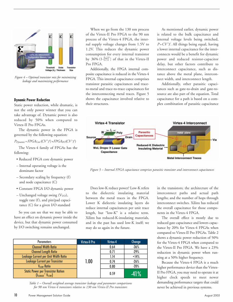
When we go from the 130 nm processof the Virtex-II Pro FPGA to the 90 nmprocess of the Virtex-4 FPGA, the inter-nal supply voltage changes from 1.5V to1.2V. This reduces the dynamic powerconsumption for every internal transistorby of that in the Virtex-IIPro FPGA.
Additionally, the FPGA internal com-posite capacitance is reduced in the Virtex-4FPGA. This internal capacitance comprisestransistor parasitic capacitances and trace-to-metal and trace-to-trace capacitances forthe interconnecting metal traces. Figure 5shows the capacitance involved relative totheir structures.
Does low-K reduce power? Low-K refersto the dielectric insulating materialbetween the metal traces in the FPGA.Lower K dielectric insulating layers doreduce internal capacitances per unit tracelength, but “low-K” is a relative term.Xilinx has reduced-K-insulating materials,and in the past has used low-K itself; wemay do so again in the future.
36% (1-[ ]2 )1.5
1.2
As mentioned earlier, dynamic poweris related to the bulk capacitance andinternal voltage levels being switched,P=CV 2ƒ. All things being equal, havinga lower internal capacitance for the inter-connects would be a benefit for dynamicpower and reduced resistor-capacitordelay, but other factors contribute tointerconnect capacitance, such as dis-tance above the metal plane, intercon-nect width, and interconnect length.
Additionally, other parasitic capaci-tances such as gate-to-drain and gate-to-source are also part of the equation. Totalcapacitance for a path is based on a com-plex combination of parasitic capacitance
in the transistors; the architecture of theinterconnect paths and actual pathlengths; and the number of hops throughinterconnect switches. Xilinx has reducedthe overall capacitance for those compo-nents in the Virtex-4 FPGA.
The overall effect is mostly due toreduced gate capacitance and lowers capac-itance by 20% for Virtex-4 FPGAs whencompared to Virtex-II Pro FPGAs. Table 2shows a dynamic power reduction of 50%for the Virtex-4 FPGA when compared tothe Virtex-II Pro FPGA. We have a 23%reduction in dynamic power when run-ning at a 50% higher frequency.
Because the Virtex-4 FPGA is a muchhigher performance device than the Virtex-II Pro FPGA, you may need to operate it athigher clock speeds to meet newerdemanding performance targets that couldnever be achieved in previous systems.
10 Power Management Solution Guide August 2005
ParametersChannel Width RatioChannel Length Ratio
Leakage Current per Unit Width RatioLeakage Current per Transistor
VCCINT RatioStatic Power per Transistor Ration
(ILEAKAGE* VCCINT)
Virtex-II Pro Virtex-4 Change0.640.711.140.740.80
0.59
-36%-29%+14%-26%-20%
1.00
-41%Table 1 – Overall weighted average transistor leakage and parameter comparisons
for 90 nm Virtex-4 transistors relative to 130 nm Virtex-II Pro transistors
Figure 4 – Optimal transistor mix for minimizingleakage and maximizing performance
Figure 5 – Internal FPGA capacitance comprises parasitic transistor and interconnect capacitances

Embedded BlocksAnother major area of improvement inpower consumption is in the area ofembedded functions. This has alwaysbeen a strength in Xilinx FPGAs, but it ismore so in the Virtex-4 FPGA, evenwhen compared to the feature-richVirtex-II Pro FPGA.
In Virtex-4 FPGAs you can take furtheradvantage of both static and dynamic powerreduction by using the embedded functions,which are built as hard-logic functions.
When embedded functions are imple-mented as hard-logic functions instead ofin configurable logic blocks and program-mable interconnects, there is a lot lessstatic and dynamic power consumed. Thisis because far fewer transistors are used forhard, fixed logic than for programmablelogic. Additionally, there are no transistorsneeded to make connections for intercon-nects in the embedded functions, becausethere are no programmable interconnects.
Xilinx has carefully studied some of thefunctions that engineers like you havestruggled with and that we have alsofound tedious to implement within the
FPGA programmable logic. The newembedded functions lower power by 80-95% compared to their configurable logicblocks and routed counterparts in pro-grammable silicon.
Comprehensive Power Planning ToolsAnother useful thing in planning power isthat Xilinx data sheets show you both typ-ical and maximum power consumptionnumbers. Maximum numbers are forworst-case process, temperature, and volt-age, but many designers are very happy towork with typical numbers, depending ontheir application and the number of partsbeing used in one system.
One additional very useful thing thatyou can take advantage of in planning forpower consumption in Xilinx FPGAs arepower planning tools. Xilinx web powertools are available for estimating powerearly in the design cycle. Also, as part of theXilinx design flow, XPower looks in moredetail at a mapped or routed design. Bothcan be found, along with power applicationnotes, by searching the Xilinx website forthe phrase “Xilinx Power Tools.”
ConclusionXilinx has made profound improvements inboth static and dynamic power in the Virtex-4 90 nm family of FPGAs when comparedto Virtex-II Pro FPGAs – and (we believe) incomparison to our competitors. We havedone this through a multi-pronged, purpose-ful approach in the areas of reduced leakagecurrent, reduced dynamic power consump-tion, and embedded functions, withoutcompromising performance. These, alongwith comprehensive power planning tools,make the Virtex-4 device an excellent choicefor a high-performance FPGA system.
For more information about power con-sumption in Virtex-4 and other XilinxFPGAs, visit www.xilinx.com/products/design_resources/design_tool/grouping/power_tools.htm.
August 2005 Power Management Solution Guide 11
ParametersVCCINT
CTOTAL (rel.)fMAX (rel.)
Power at Same Frequency
Power at fMAX
Virtex-II Pro Virtex-4 Change1.20.81.5
1.15
1.73
1.51.01.0
2.25
2.25
-20%-20%+50%
-23%-49%
Parameters
QDR II SRAM Interface
SPI-4.2 Core
Virtex-II Pro Virtex-4Logic SliceReduction
Logic SlicePower Reduction
550 slices 125 slices 77% 89%5000 slices 3900 slices 22% 61%
Logic slice power reduction = 100* 1 – 0.5Virtex-4 slice count
Virtex-II Pro slice count( )%
Note: The factor of 0.5 above comes from the fact that Virtex-4 power per slice is 1/2 of the Virtex-II Pro power per slice because of the 50% dynamic power reduction in Virtex-4 devices compared to Virtex-II Pro devices.
Table 2 – Chart showing changes in internal FPGA in Virtex-4 devices compared to Virtex-II Pro devices and the effect on dynamic power
Table 3 – QDR II SDRAM and SPI-4.2 core benefit in reduced power consumption from significant logic cell reduction due to new Virtex-4 ChipSync block
Virtex-4 Embedded Functions andReduction of Dynamic Power
• PowerPC – 50% power reductioncompared to Virtex-II Pro PowerPC
– 10:1 power reduction over FPGAfabric-built version
• DSP – XtremeDSP™ slice greatlyreduces logic cells, which previously needed many filtering functions
– 20:1 power reduction over Virtex-IIPro separated multiply/accumulatefunctions
• SSIO – New ChipSync™ blockreduces logic cell count for SSIO(source synchronous I/O) designs
– Significant logic cell savings for vari-ous memory and networking inter-face designs leads to reduction inoverall power up to 9:1 for selecteddesigns (see Table 3)
• Embedded Ethernet MAC(s) – Noneed to use logic and interconnectfor MAC function, which saves>3,000 logic cells for the Xilinximplementation
• FIFO – SmartRAM™ memoryincludes built-in FIFO controllers,which can save hundreds of logiccells per FIFO and greatly simplifydesign as well


August 2005 Power Management Solution Guide 13
© 2005 Xilinx, Inc. All rights reserved. XILINX, the Xilinx logo, and other designated brands included herein are trademarks of Xilinx, Inc.All other trademarks are the property of their respective owners.
The debate over which high-performance 90 nmFPGA has the lowest power is “heating up,” and forgood reason. The industry has crossed a criticalinflection point at 90 nm, where performancecompetes with power and thermal budgets.Customers want as much performance as possible;increasingly, however, the decision about whichFPGA to use is based on which device consumes theleast amount of power. This white paper discussesperformance versus power consumption in 90 nmFPGAs and how the Virtex™-4 family provides thebest of both worlds: high performance and lowpower consumption.
White Paper: Virtex-4 Family
WP223 (v1.1) May 12, 2005
Power vs. Performance:The 90 nm Inflection Point
By: Anil Telikepalli
R

14 Power Management Solution Guide August 2005
White Paper: Power vs. Performance: The 90 nm Inflection PointR
Introduction Excessive power is expensive in many ways. It creates the need for special design andoperational considerations – requiring everything from heat sinks to fans to sophisticated heat exchangers. Even the cost of building larger power supplies must be taken into consideration. Overall, increased power requires more of everything, including: more area on the PCB, a larger chassis, more floor space, and larger air conditioning systems. The costs continue to compound.Perhaps the most critical issue is the effect excessive power can have on reliability. As the junction temperatures rise, transistors consume more power, thereby further increasing the temperature of the device. Continuously operating systems with junction temperatures running from 85°C to over 100°C increases reliability issues. Fortunately, Xilinx encountered the first evidence of this 90 nm inflection point in the early development stages of Spartan™-3 FPGAs, the first Xilinx FPGA family for the 90 nm process. Xilinx began immediately developing new ways to cope with the inherent power issues posed by the 90 nm process. Consequently, when the higher-performance Virtex-4 family was introduced in September 2004, Xilinx was confidentthat the new family would simultaneously deliver the best of both worlds – the highest performance and lowest power consumption in a 90 nm FPGA.
Reducing Power in FPGAs
The Triple ChallengeThere are two major components to power consumption in FPGAs: static power, anddynamic power. Inrush current is another factor that can occur when the FPGA ispowered on. Each component poses a unique challenge. For the 90 nm FPGA, the most challenging component is static power.
Static PowerStatic power consumption occurs as a result of leakage current in the transistors thatcomprise the FPGA. As transistors get smaller (with each new process), their leakagecurrent increases. This principle is one of the major reasons the 90 nm process crossesa major inflection point (Figure 1).
Figure 1: 90 nm Inflection Point
1990 1995 2005 2010 2015 20200.0000001
0.0001
0.01
1
100500 350 180 90 45 2265130250
InternationalTechnology Roadmapfor Semiconductors(ITRS) 2001, 2002.Courtesy: Moore’s LawMeets Static Power,Computer, December 2003,IEEE Computer Society
Static Power Significant at 90 nm
No
rmal
ized
Po
wer
Technology Node (nm)
Static Power (leakage)
2000
Dynamic Power
wp223_01_040705

August 2005 Power Management Solution Guide 15
White Paper: Power vs. Performance: The 90 nm Inflection PointR
For the first time, static power is threatening to eclipse dynamic power as the component responsible for the greatest amount of total power consumption in an FPGA. This is partly due to the fact that as processes get smaller, the core voltagedecreases; consequently, the rate of increase in dynamic power drops, despite the increase in frequency that regularly accompanies a new process. In contrast, below 0.25 microns static power has grown exponentially with each new process.This is where the inflection point really becomes a critical factor for the FPGAs and where Xilinx has established a substantial lead. Smaller transistors are faster, but they leak more. However, unlike ASICs, ASSPs, and microprocessors, Xilinx FPGAs do not need all of their transistors to switch at maximum speed. A substantial number of transistors comprise the configuration memory cells used to select logic and routing, and pass transistors used to implement the programmable interconnect routing.Configuration memory cells do not need to be fast, and programmable interconnect transistors only need to be fast from source to drain and not under gate control. Thesefactors allow leakage to be reduced without compromising performance.Virtex-4 FPGAs take advantage of the abundance of these particular types of transistors to incorporate a new process approach called “triple-oxide technology” to solve the static power problem. Figure 2 shows how Virtex-4 FPGAs consume 50% lower static power than its predecessor, the 130 nm Virtex-II Pro FPGAs.
What is Triple-Oxide Technology?For many years, Xilinx and other semiconductor vendors have used two gate-oxide thicknesses: a standard thin layer used for the vast majority of transistors and a thickoxide layer for I/O drivers. With the introduction of Virtex-4 FPGAs, Xilinx has utilized triple-oxide, which refers to a third thickness of gate oxide used in making the configuration memory cells and pass transistors.Oxide deposition thickness is a very stable and controllable process in the semiconductor industry. Semiconductor manufacturers can accurately set oxide thickness by choosing temperature, concentration, and exposure time. Figure 3 shows the Virtex-4 transistor with the middle oxide thickness used in the triple-oxide process. Although this third oxide layer is still very thin, these transistors exhibit substantially lower leakage than the standard thin-oxide low VT and regular VTtransistors used in Virtex-II Pro FPGAs and in various other parts of Virtex-4 FPGAs.
Figure 2: The use of "triple oxide" technology reverses the trend: the Virtex-4 deviceactually consumes less static power than its 130-nm predecessor.
0 200K25K
XC2VP20
XC2VP100
XC4VLX25
XC4VLX100
XC4VLX200
50K 75K 100K
Logic Cells
Rel
ativ
e S
tatic
Pow
er(W
orst
Cas
e P
roce
ss @
85°
C)
125K 150K 175K
6
5
4
3
2
1
0
Virtex-4
50% Lower Power
Virtex-II Pro
wp223_02_040805

16 Power Management Solution Guide August 2005
White Paper: Power vs. Performance: The 90 nm Inflection PointR
In addition to using triple-oxide, Xilinx optimized a number of other transistor parameters to balance performance and leakage across I/O, configuration memory, interconnect pass transistors, as well as logic and interconnect buffers (Table 1).
The use of triple-oxide technology in Virtex-4 devices dramatically reduced the static power component for the entire family.Other optimizations were made to reduce leakage and hence, static power. These include enhancements to gate length, VT and oxide thickness. The combination of these effects on leakage and performance is shown in Figure 1.As mentioned earlier, a comparison of relatively equivalent devices from both the 130 nm Virtex-II Pro family and the 90 nm Virtex-4 family reveals 50% less static power consumed by the Virtex-4 device (Figure 2). This is the first time in FPGA history that static power decreased when moving to a new smaller process. Incontrast, Stratix II FPGAs consume two times more power than previous 130 nmStratix FPGAs (Figure 4).
Figure 3: Virtex-4 Transistor Middle Oxide Thickness
Source Channel Drain
Gate
Source MetalConnection
Drain Metal Connection
wp223_03_040705
Triple-Oxide Technology
Three varyinggate oxidethicknesses
Table 1: Triple-Oxide Technology and Other Transistor Parameters Used for Power Optimization
Function Oxide ThicknessVoltage Threshold
(VT)Channel Length Speed Leakage
I/O Thick High Longest Fast LowestConfig Memory Medium Medium Long Slow LowInterconnect Pass Gates
Medium Low/Medium Short Fast
SourceDrain
Low
Logic and Interconnect Buffers
Thin Low Short Very Fast Medium/High

August 2005 Power Management Solution Guide 17
White Paper: Power vs. Performance: The 90 nm Inflection PointR
Dynamic PowerThe three contributing elements to dynamic power in the FPGA core are voltage,frequency, and parasitic capacitance. Fortunately, as previously mentioned, the corevoltage and capacitance decrease with each new smaller process, which lowers dynamic power. If designs require higher operating frequencies, dynamic powerincreases. The well-known formula for dynamic power that applies here is:
P = CV2f Equation 1
In addition, dynamic power is proportional to the data toggle rate.One major area of improvement in power consumption is in the area of embeddedfunctions. This has always been a strength in Xilinx FPGAs, but it is more so in the Virtex-4 FPGA, even when compared to the feature-rich Virtex-II Pro FPGA. When embedded functions are implemented as hard-logic functions instead of configurable logic blocks and programmable interconnects, less static and dynamicpower are consumed. This is because far fewer transistors are used for hard, fixed logic rather than programmable logic. Additionally, transistors are not needed for interconnects in the embedded functions, because there are no programmable interconnects. These hard IP cores occupy far less real estate, deliver much higher performance, andconsume 80-95% less power than soft IP versions of the same functions. In addition, by making these hard IP cores programmable and parameterizable, Xilinx provides designers with the flexibility they have come to expect from an FPGA. No other FPGA vendor provides so many hard IP cores for common functions.Functions that Xilinx provides as hard IP cores in Virtex-4 FPGAs include:• 450 MHz PowerPC™ processors for all microcontroller and embedded processing
applications with an APU interface for hardware acceleration. A soft implementation would invariably consume several thousand look-up tables (LUTS) and flip-flops (FFs). Virtex-4 PowerPC processors also contain their own dedicated 16 Kbyte instruction and 16 Kbyte data cache. In addition to providing much better performance, these optimized cache memories consume much less power than building the equivalent-sized cache out of internal FPGA block memory.
• 500 MHz XtremeDSP™ slice for simple math and filters to complex high-performance DSP functions. With 40 op-modes and the ability to cascade multiple
Figure 4: Stratix-II Exhibits a Typical Increase in Worst-case Static Power Consumption Expected in Transitioning to the 90 nm Process – Without Triple-Oxide!
0 25K 50K 75K 100K 125K 150K 175K 200K
1S802S15
2S180
Logic ElementsR
elat
ive
Wor
st C
ase
Sta
tic P
ower
8
7
6
5
4
3
2
1
0Stratix
2X Higher PowerStratix-II
wp223_04_040805

18 Power Management Solution Guide August 2005
White Paper: Power vs. Performance: The 90 nm Inflection PointR
slices without extra logic, each DSP slice functionality implemented as a soft corewould cost anywhere from tens to hundreds of LUTs and FFs.
• 500 MHz Digital Clock Managers (DCM) and Phase Matched Clock Dividers (PMCD) that support clock synthesis, clock management, and phase matching. Unlike embedded PLLs, DCMs and PMCDs do not require special supply rails.
• ChipSync™ block in every I/O with built-in SERDES and data-alignment function to simplify source-synchronous interfaces in memory, networking, and telecom applications. Implemented as soft IP, each ChipSync block control circuitry would consume tens to hundreds of LUTs and FFs.
• 622 Mb/s - 10.3125 Gb/s RocketIO™ transceivers with built-in Physical Coding Sublayer (PCS) and Physical Media Attachment (PMA). With support for 8B/10B, 64B/66B, custom coding, elastic buffers, clock-data recovery, and multiple equalization options, implementing this functionality in soft IP would cost thousands of LUTs and FFs per transceiver. An external SERDES typically consumes much more power because the FPGA to external SERDES is typically high-performance parallel I/O. These parallel I/O can burn far more power than the Serial I/O channels.
• Tri-mode Ethernet MACs that run at 10/100/1000 Mb/s and can interface directly with RocketIO transceivers. Here again, a soft IP implementation would consume a few thousand LUTs and FFs.
• Smart RAM memory with distributed RAM and block RAM. Each LUT has built-in circuits to turn it into a distributed RAM/ROM, as well as a 16-bit shift-register. Each block RAM has built-in ECC for error correction and built-in control circuits to implement an asynchronous FIFO. All this functionality implemented in soft IP would consume hundreds of LUTs and FFs per block RAM.
Besides the obvious advantages associated with moving these commonly used blocksinto hard IP, one must not overlook the inherent contribution the Xilinx Advanced Silicon Modular Block (ASMBL) architecture makes to the Virtex-4 dynamic power advantage. Because each of the three families – the LX, FX, and SX – is meant to satisfy distinct requirements for a particular application domain (logic, embedded processing, and signal processing), their standard ratio of logic cells, memory, I/O, DSP, processors, etc., has been optimized for that domain. Consequently, the Virtex-4device is the first FPGA to offer domain-optimized dynamic power consumption (Table 2).
Inrush CurrentWhen voltage is initially applied to an FPGA, its internal circuitry undergoes states of ambiguity while configuration storage latches and other circuits are programmed sequentially. The internal contention that occurs during powerup can produce spikesof inrush current that measure in multiple amps. This inrush current often requires the
Table 2: The Virtex-4 Domain-optimized Functions that Substantially Improve Dynamic Power Efficiency
Functions Virtex-4 LX Virtex-4 SX Virtex-4 FX
Logic Cells 14 to 200K 23 to 55K 12 to 140KEmbedded Memory 0.9 to 6 Mb 2.3 to 5.7 Mb 0.6 to 10 MbDCMs 4 to 12 4 to 8 4 to 20XtremeDSP Slices 32 to 96 125 to 512 32 to 192SelectIO Signalling 240 to 960 320 to 640 240 to 896RocketIO Transceivers N/A N/A 0 to 24 channelsPowerPC Processors N/A N/A 1 or 2 processorsEthernet MACs N/A N/A 2 or 4 embedded blocks

August 2005 Power Management Solution Guide 19
White Paper: Power vs. Performance: The 90 nm Inflection PointR
use of expensive regulators, and larger, more expensive power supplies. To properly configure the FPGA, the power supply must be able to handle the large in-rush currents even if the device operates at much lower dynamic current levels duringoperation. This is especially true if the clock frequency of the FPGA during normal operation does not push the maximum limits.Xilinx eliminated nearly all inrush current in Virtex and Spartan series FPGAs a fewyears ago by embedding innovative housekeeping circuitry to prevent this contention from occurring.
PowerEstimations
The heat of competition in the FPGA marketplace can sometimes make it difficult for customers to obtain objective, fair-handed assessments of performance and power claims. So how does one determine which high-performance 90 nm FPGA family consumes the lowest total power, including static and dynamic power measured at the design’s operating temperature?
In an attempt to keep a level playing field and the comparisons on an apples-to-apples basis, the Xilinx Web Power Tool v4.1 based on extensive characterization data was used to estimate power for the Virtex-4 devices. Altera’s PowerPlay 2.1 powerestimation tool was used to do the same for relatively equivalent logic density Stratix II parts. To keep the static power comparison simple, only the core voltage supply is examined. Temperature invariant auxiliary voltage supplies (VCCAUX and VCCPD) are intentionally excluded. Stratix II FPGAs require additional voltage supply rails and power for every PLL used – these are also not included in the comparison.If a hard IP block is available in Stratix II, it is used in the comparison; if not, the equivalent soft IP, using the logic utilization published for Stratix II implementations, is used. Because Virtex-4 FPGAs have more hard IP functions than Stratix II, and each hard IP function has more programmable features and options than Stratix II, it is difficult to compare “equivalent” functions; however, the comparison was executedon as much of an “apples-to-apples” basis as driven by the products.The following results are offered for consideration, and since both tools are readily available, everyone is encouraged to perform the same or similar comparisons themselves. The results are compelling.
66% - 73% Less Static PowerFigure 5 compares the static power at Tj = 85°C using Xilinx WPT v4.1 vs. Stratix IIPowerPlay v2.1. Table 4 shows the detailed data.
Figure 5: Static Power Estimations
XC4VLX
15
Sta
tic P
ower
Devices with Equivalent Logic Cells
Virtex-4 FPGAsStratix II FPGAs
wp223_05_040805
66%67%67%67%71%73%
2S15
XC4VLX
252S
30
XC4VLX
602S
60
XC4VLX
802S
90
XC4VLX
100
2S13
0
XC4VLX
160
2S18
0
20 Power Management Solution Guide August 2005
White Paper: Power vs. Performance: The 90 nm Inflection PointR
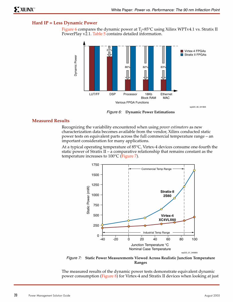
Hard IP = Less Dynamic PowerFigure 6 compares the dynamic power at Tj=85°C using Xilinx WPTv4.1 vs. Stratix II PowerPlay v2.1. Table 5 contains detailed information.
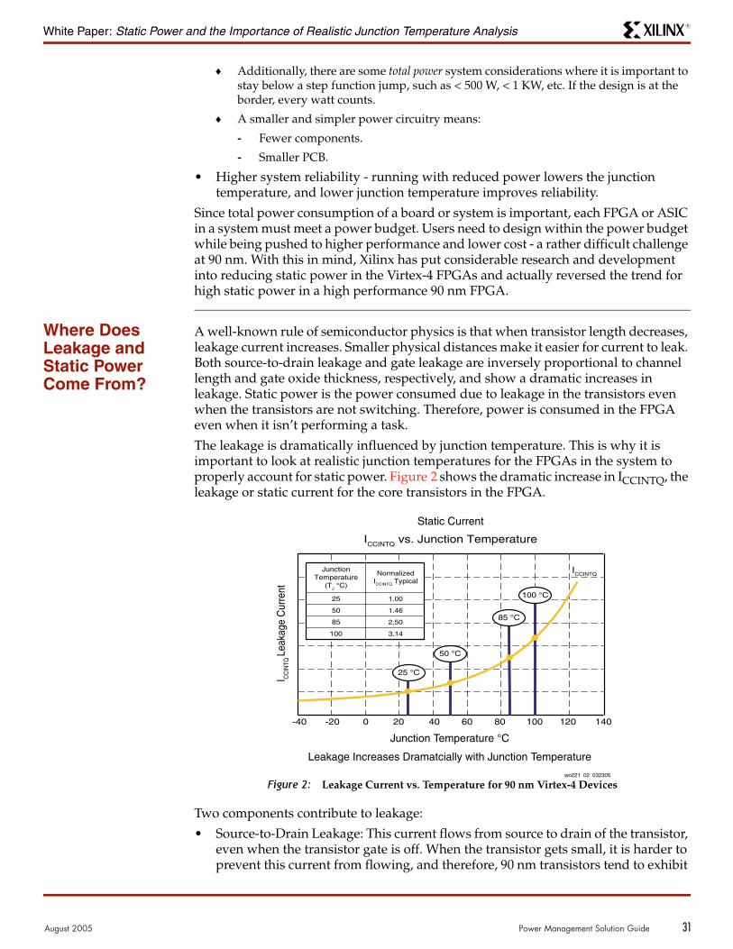
Measured ResultsRecognizing the variability encountered when using power estimators as newcharacterization data becomes available from the vendor, Xilinx conducted static power tests on equivalent parts across the full commercial temperature range – an important consideration for many applications.At a typical operating temperature of 85°C, Virtex-4 devices consume one-fourth thestatic power of Stratix II – a comparative relationship that remains constant as the temperature increases to 100°C (Figure 7).
The measured results of the dynamic power tests demonstrate equivalent dynamic power consumption (Figure 8) for Virtex-4 and Stratix II devices when looking at just
Figure 6: Dynamic Power Estimations
LUT/FF DSP Processor 18KbBlock RAM
EthernetMAC
Dyn
amic
Pow
er
Various FPGA Functions
Virtex-4 FPGAsStratix II FPGAs
wp223_06_041805
83%82%86%
23%
Figure 7: Static Power Measurements Viewed Across Realistic Junction Temperature Ranges
Commercial Temp Range
40 60 80 100-40 -20 0 20
Junction Temperature °CNominal Case Temperature
Sta
tic P
ower
(m
W)
1750
1500
1250
1000
750
500
250
0
Stratix-II2S60
Virtex-4XC4VLX60
wp223_07_040805
Industrial Temp Range

August 2005 Power Management Solution Guide 21
White Paper: Power vs. Performance: The 90 nm Inflection PointR
LUTs and FFs. A more dramatic result (Figure 9) is obtained when testing block RAM configurations of equivalent sizes. In large part, the difference is due to the availabilityof optimally sized 18K bit memories from Xilinx. The smaller Stratix II 4K bit block RAMs consume nearly the same amount of power as the Virtex-4 18K bit block RAMs.Most customer designs either need ultra-small distributed RAM or medium-level memories built using 18K bit blocks – prompting Xilinx to move from 4K bit memories three product generations ago.Although Stratix II FPGAs also have DSP blocks that can be connected using adder trees built out of logic resources, the Virtex-4 XtremeDSP slice provides the unique advantage of cascading multiple slices without additional logic. For many DSP functions, this gives a big advantage on speed and power. To test the dynamic power for DSP designs, a 64-tap FIR filter is used. The filter has 63 section asymmetrical taps with 18-bit data stream and fixed 18-bit coefficients. The Virtex-4 FPGA uses 63 XtremeDSP slices in a single column; one slice is used for stimulus. The Stratix II FPGA uses four tap sections in each DSP block, which are added together using nine 3-input adder tree structure. Stratix II ALMs are used for stimulus. Figure 10 shows the Virtex-4 FPGA consuming 2.35x (or 60%) lower dynamic power than Stratix II for DSP designs.The more astonishing result is found for the VCCINT core voltage and the VCCAUX(2.5V) in the Virtex-4 device and the VCCPD (3.3V) supply in Stratix II. The VCCAUX in the Virtex-4 FPGA is used for configuration memory (some in DCMs, and some in I/O pre-drivers). The VCCPD supply in Stratix II is used for configuration and I/O pre-drivers. In order to test I/Os, 500 LVCMOS I/Os were tested at all voltage levels (1.5V,2.5V, and 3.3V). All outputs are in DDR mode, and loads are terminated to ½ VCCIO. DC to 400 MHz frequency range was used. Shown in Figure 11, the Virtex-4 deviceconsumes lower power at all voltage levels.In Figure 12, VCCPD supply consumes four times the power of the VCCAUX supply —translating into Watts of power difference! The VCCINT supply in Stratix II also consumes three times the static power and 50% more dynamic powerThe conclusion about the tests is that the Virtex-4 device consumes much less power than Stratix II.

22 Power Management Solution Guide August 2005
White Paper: Power vs. Performance: The 90 nm Inflection PointR
Dynamic Power – Fabric
Dynamic Power – Memory
Dynamic Power - DSP (64-Tap FIR Filter)
Figure 8: Fabric Test with 25,000 LUT/ALUTs and 21,000 FFs (High Toggle Rate). Allmeasurements were taken at Tj = 85ºC.
Figure 9: FIFO/Block RAM test with 252 M4K in Stratix II and 63 Block RAM in Virtex-4FPGAs (same total storage). All measurements were taken at Tj = 85º C.
Figure 10: DSP Test: 64-Tap FIR Filter
300250200150100500Frequency (MHz)
Pow
er (
Wat
ts)
7.0
6.0
5.0
4.0
3.0
2.0
1.0
0.0
Virtex-4 XC4VLX60
Stratix II 2S60
wp223_08_040805P
ower
(W
atts
)
5.0
4.5
4.0
3.5
3.0
2.5
2.0
1.5
1.0
0.5
0.0
Virtex-4 XC4VLX60
Stratix II 2S60
300250200150100500
Frequency (MHz)wp223_09_040805
1.0
0.8
0.5
0.3
0.00 50 100 150
Frequency (MHz)
Pow
er (
Wat
ts)
200 250 300
2.35x
Virtex-4 LX60
Stratix II 2S60
WP223_10_041905

August 2005 Power Management Solution Guide 23
White Paper: Power vs. Performance: The 90 nm Inflection PointR
Dynamic Power - I/O .
Total PowerBudget Comparison
Another simple way to obtain a high-level comparison of power consumption in FPGAs is to assess the available performance and power headroom for a given power budget and target frequency. For this comparison, popular applications for high-performance FPGAs at a sweet-spot density of 60,000 logic cells were considered, e.g.,multi-service provisioning platforms in networking and telecom access markets; blade servers in storage and server markets; line cards in wireless base stations; and control cards in industrial and military/aerospace systems. Operating at an average target frequency of 200 MHz, with operating temperatures in the range of 65-100ºC, thepower budget for these applications is typically 6W per FPGA.
Using these applications as an example, the Virtex-4 FPGA meets the target frequency,well within the power budget at 4.9W. On the other hand, Stratix II FPGAs exceed thepower budget, consuming 7.9W at the target frequency. Consequently, when constrained by the 6W power budget, Stratix II delivers only 133 MHz performance (Figure 13).
Figure 11: Virtex-4 FPGAs Consume Less Power at All Three VCCIO Voltages
Figure 12: I/O Test: Stratix II shows 1.5x the VCCINT Dynamic Power and 4x the VCCPD/VCCAUX Power compared to the Virtex-4 FPGA
100
40
50
60
70
80
90
30
20
10
00 100
Frequency (MHz)
Pow
er (
mW
) -
The
veni
n Lo
ad P
wr
200 300
VCCO = 1.5 V
VCCO = 2.5 V
VCCO = 3.3 V
VCCO = 1.5 V
VCCO = 2.5 V
VCCO = 3.3 V
400
Virtex-4
Stratix II
WP223_11_041805
10
4
5
6
7
8
9
3
2
1
00 100
Frequency (MHz)
Pow
er (
W)
- F
or V
CC
INT a
ndV
CC
AU
X/V
CC
PD
200 300
VCCINT = 1.2 V
VCCAUX = 2.5 V
VCCINT = 1.2 V
VCCPD = 3.3 V
400
4.0x
Virtex-4
Stratix II
WP223_12_042005
1.5x

24 Power Management Solution Guide August 2005
White Paper: Power vs. Performance: The 90 nm Inflection PointR
Xilinx Telecom Customer’sSPI4.2 Design Comparison
Intrigued by the power consumption advantages in Virtex-4 devices, one Xilinx customer used the web power estimation tools to compare the power consumption for a SPI4.2 core implemented on Stratix II and Virtex-4 FPGAs.
The Optical Internetworking Forum's SPI4.2 parallel interface appears in numerous10-Gb/s networking and telecom applications. Because virtually all networking andtelecom equipment has stringent power and thermal budgets, the customer waspleased to discover that the estimators showed Virtex-4 devices consuming 50% lowertotal power than Stratix II for this application.Satisfied but surprised by the results, the customer decided to perform real measurements on actual implementations to verify the findings. Once again, this timewith actual lab results in hand, the customer found that Virtex-4 FPGAs consumed 50% lower total power for the SPI4.2 implementation than did the Stratix II version.The Xilinx customer’s test has been recreated using similar conditions, with similar results. The results are presented in Figure 14 and Table 3.
Figure 13: Customers Select the High-performance FPGA that Best Meets Their Power Budget
Performance (MHz)
Tot
al P
ower
(W)
1
2
3
4
5
6
0
7
100 150 200 250500
8
9
Virtex-4FrequencyHeadroom
Virtex-4Power
Headroom
Virtex-4
Stratix II
Design Example
Virtex-4 Total Power 4.9W
Stratix II Total Power 7.9W
Requirements- Power Budget = 6 Watts per FPGA- Target Frequency = 200 MHz- Worst case condition at TJ = 85˚C
128x LVCMOS 2.5V128x LVCMOS 2.5V
Stratix II 2S60Virtex-4 LX60
20K ALUT/FF20K LUT/FF
252x M4K RAM63x 18Kb Block RAM
64x DSP Blocks64x DSP Slices
wp223_13_042505
Figure 14: Customer Analysis on SPI4.2 Power Consumption
XC4VLX25 2S30 XC4VLX60 2S60
Tota
l Pow
er
Virtex-4 FPGAs in FF668 packageStratix II FPGAs in F672 package
wp223_14_041805
49%
50%3.4W
1.7W
4.2W
2.1W
SPI4.2 800 Mbps, 1 port, 128-bit User Interface

August 2005 Power Management Solution Guide 25
White Paper: Power vs. Performance: The 90 nm Inflection PointR
Note: Limited data available on the Stratix II implementation. For fair comparison, some assumptions had to be made about clocks. See Answer Record 20430 on Xilinx.com for Virtex-4 SPI4.2 power.
1 to 5 Watts lower power per FPGA
Having demonstrated substantial power savings – both in static power as a result of triple-oxide technology and in dynamic power using embedded IP – and having presented corroborating results from both power estimators and lab measurements using various designs, one might well ask, “What does it all mean for my design?”
The simplest example provides the best perspective. Using an equivalent amount ofgeneric logic and memory in Virtex-4 and Stratix II devices of equivalent density, with no consideration of other embedded IP, the Virtex-4 FPGA saved 1 - 5W in power. A design should realize at least this much power savings per every Virtex-4 FPGA used, if not better.The results are shown in Figure 15. To present the lowest bar in power savings, benefits from extensive hard IP in Virtex-4 FPGAs were not included.
Table 3: Virtex-4 vs. Stratix II Implementation
Virtex-4 Implementation Stratix II Implementation
Protocol SPI4.2 v7.2, 800 Mb/s SPI4.2 v2.2.2, 800 Mb/s
User I/F 128-bit, 1 port 128-bit, 1 port
Logic 3750 Slices: 4893 LUTs 25% toggle rate used
Tx and Rx: 10844 ALUTs (calculated from 10968 + 2588 LEs) 25% toggle rate used
Memory 306 Kb total – 17 18Kb-block RAMs used: 13 - 512 x 36 2 - 36 x 512 write and 18 x 1024 read 2 - 1024 x 9 25% toggle rate used
244 Kb total – 62 block RAMs used: 61 - M4K blocks 1 - M512 blocks 25% toggle rate used
LVDS 17 LVDS pairs for Rx and Tx: 35 pF average load Additional differential clock output
17 LVDS pairs for Rx and Tx: 35 pF average load Additional differential clock output
Clock Frequency(Assumption)
200 MHz single clock 200 MHz single clock
Figure 15: Virtex-4 Designs Consume 1 to 5 Watts Lower Power per FPGA
Static Power at TJ = 85˚C
Dynamic Power at 200MHz- 50% of LUTs & FFs in Virtex-4 device; equivalent ALUTs & FFs in correspondingStratix II device.12.5% toggle rate.
- All M4K blocks used in Stratix II device; equivalent 18Kb block RAM in corresponding Virtex-4 device
Design Details - Logic & Memory 10.0
8.0
6.0
2S15
Pow
er (W
)
4.0
2.0
0.0
Virtex-4Stratix II
wp223_15_042505
Total Power Consumption14.0
12.0
XC4VLX15
2S30
XC4VLX25
2S60
XC4VLX60
2S90
XC4VLX80
2S13
0
XC4VLX10
02S
180
XC4VLX16
0

26 Power Management Solution Guide August 2005
White Paper: Power vs. Performance: The 90 nm Inflection PointR
Power Struggle The battle to deliver maximum performance with minimum power expenditure hastaken center stage in the evolution of the FPGA. Power conservation impacts everybudget, whether technological or financial. Product acceptability, reliability and profitability depends as much or more on power efficiency as it will on performance. Virtex-4 FPGAs not only have a far superior feature set, but also exhibit a real power consumption advantage. The choice should be very clear for designers who require lower power consumption, and high-performance and functionality. Initial test results tell the story:• Up to 73% lower static power with the industry’s first triple-oxide technology• Up to 86% lower dynamic power with high-performance embedded IP The competition in the market does not end with 90 nm devices. Some interesting new dynamics arise when moving into a 65 nm node and below. Fortunately for Xilinx, one inherent value of using triple-oxide technology is that it scales nicely with each new process. As for the value of embedding hard IP wherever appropriate, it is practically an industry axiom. Xilinx has incorporated the right amount of programmableembedded IP with programmable logic to make the whole solution more flexible with higher-performance, and lower power. In the long term, customers will use only Platform FPGAs that provide the best of performance and power.
Appendix
Static Power Comparison DataTable 4 gives the comparison data for static power.
• Core static power = ICCINTQ x VCCINT. Altera data is based on PowerPlay tool v2.1 on www.altera.com. Static power for VCCPD (the Stratix II VCCAUX supply) and VCCIO does not change with temperature and is not shown. Stratix II also consumes additional power for PLL supply rails that are not shown.
• Devices of equivalent logic density are compared.
Table 4: Static Power Comparison Data
Virtex-4 Static Power Stratix II Static Power Virtex-4 Power Reduction
Typical 25°C/85°CVirtex-4 Device Typical 85°C Tj Stratix II Part Typical 85°C Tj
XC4VLX15 138 mW 2S15 515 mW 73%
XC4VLX25 231 mW 2S30 792 mW 71%
XC4VLX60 493 mW 2S60 1,478 mW 67%
XC4VLX80 640 mW 2S90 1,960 mW 67%
XC4VLX100 863 mW 2S130 2,630 mW 67%
XC4VLX160 1,117 mW 2S180 3,310 mW 66%

August 2005 Power Management Solution Guide 27
White Paper: Power vs. Performance: The 90 nm Inflection PointR
Dynamic Power Comparison DataTable 5 gives the comparison data for dynamic power.
Table 5: Dynamic Power Comparison Data
Virtex-4 Dynamic Power (Room Temperature)
Stratix II Dynamic Power (Room Temp)Virtex-4 Power Reduction
Function at 200 MHz Power Function at 200 MHz Power
1 LUT and 1FF 30% toggle rate Medium Routing
0.15 mW 1 ALUT and 1 FF 30% toggle rate Routing data unavailable
0.15 mW ~same
1 XtremeDSPSlice 18x18 MAC Registered in/out Medium (55%) toggle rate
6.6 mW 1 DSP Block 18 x18 MAC Registered in/out 50% toggle rate
8.57 mW 23%
PowerPCProcessor 16Kb I-Cache and D-Cache 2 DCMs
120 mW Soft Processor 1 - 6K I-Cache and D-Cache
879 mW 86%
18 Kb block RAM Width = 18, Depth = 1 50% read and 50% write
6.16 mW Equivalent M4K RAM Width = 18, Depth = 1 50% read and 50% write
33.98 mW 82%
Ethernet MAC - embedded 1 Gb/s, 125 MHz
27 mW Ethernet MAC - soft 1 Gb/s, 125 MHz 2500 ALUTS and 2500 FFs
160 mW 83%

Power Across the Board
LM2852Y
PVINSNS
SWEN
PGNDSGND
CIN = 22 µF
VIN = 2.85V to 5.5V
CSS = 2.7 nF
LO = 10 µH
VOUT down to 0.8VILOAD = 0A to 2A
AVIN
SS CO = 100 µF+
LM2745
SS/TRK
EAO GND
VCC
ISEN
3V to 6V
ON
OFF
Output power good
Input power
1V to 16V
VOUT = O.6V to 0.85VIN
Up to 25A loadsSD
(Bias)
PGOOD
HG
FB
LG
SYNC External Clock
Up to 1 MHz
50 kHz to 1 MHzoperating frequency
Unique current sense provides over current and short circuit protection
All ceramic or electrolyticcapacitors
Dual-purpose soft start or tracking pin
Can operate from 1.8 VIN with bias
Precision enable and sequencing
LM2852 Features• Best-in-class 60 mΩ switches provide over
95% efficiency
• Factory-programmable EEPROM for any output voltage between 0.8V to 3.3V
• Up to 1.5 MHz internal compensation easesdesigning with a variety of output capacitors
• Available in thermally enhanced, ETSSOP-14 package
LM2852 Simple SynchronousTM
2A Buck Regulator
Optimize Design of Xilinx FPGA, ASIC, and Point-of-Load Power Applications
© National Semiconductor Corporation, 2005. National Semiconductor, , and WEBENCH are registered trademarks and SIMPLE SYNCHRONOUS is a trademark of National Semiconductor. All rights reserved.
For free samples, evaluation boards, datasheetsand online design tools, visit us today at:
power.national.com
LM2745 Feature-Rich Switching Controller
Or call 1-800-272-9959
Solutions for Xilinx FPGAsDesign guides, app notes, and online toolsfor Xilinx FPGAswww.national.com/see/xilinxfpga
LM2745 Features• Output voltage adjustable down to 0.6V
• Switching frequency from 50 kHz to 1 MHz
• Startup with a pre-biased load prevents sagging of output
• Available in a TSSOP-14 package
Ideal for FPGA/DSP applications in networking,telecommunications, enterprise, and automatedtest and measurement applications

August 2005 Power Management Solution Guide 29
© 2005 Xilinx, Inc. All rights reserved. XILINX, the Xilinx logo, and other designated brands included herein are trademarks of Xilinx, Inc.All other trademarks are the property of their respective owners.
Total power consumption of a board or system isimportant; each FPGA or ASIC in a system isbeginning to be forced to meet a power budget. Withthis concern and the trend of increasing static powerwith use of high performance 90 nm FPGAs, Xilinxhas put considerable effort into reducing staticpower in the Virtex™-4 FPGAs. To this end, it isimportant to consider a realistic operatingtemperature for the FPGAs, which can easily havejunction temperature up to and in excess of 85°C. Asjunction temperature rises, static power risesexponentially, fueling this concern.
White Paper: Virtex-4 Family
WP221 (v1.0) March 23, 2005
Static Power and the Importance of Realistic Junction Temperature
Analysis
By: Matt Klein
R

30 Power Management Solution Guide August 2005
White Paper: Static Power and the Importance of Realistic Junction Temperature AnalysisR
Introduction Customers expect FPGA and ASIC vendors to reduce cost and increase performance. Typically, this was achieved in the past by reducing transistor sizes, hence increasingthe performance and decreasing the die area and cost.
Reducing transistor sizes increases transistor leakage current, and therefore static power. With 90 nm technology in FPGAs or ASICs, there is a particular challenge to reduce static power. A further problem is that leakage rises dramatically with junction temperature. This white paper describes where static power comes from and itsvariation with temperature, providing insight into how Virtex-4 FPGAs address decreasing static power. Xilinx leverages its vast experience as the industry leader, producing millions of 90 nm FPGAs, to research this issue and consequently reducepower in 90 nm Virtex-4 FPGAs.
Even though system speeds are increasing, core voltage is dropping, which reduces the rate of increase of dynamic power; however, static power is growing exponentially over time as we move to smaller and smaller technology nodes because of increasing transistor leakage. Figure 1 from the International Technology Roadmap forSemiconductors (ITRS) shows a cross-over point as the industry arrives at 90 nm and smaller technology nodes, where static power is beginning to eclipse dynamic powerfor many applications.
Decreased Power Lessens Other System Design Issues
FPGAs are being used increasingly in many applications, so reducing power consumption in FPGAs provides huge benefits to the system design. Some of the key benefits are shown below:
• Fewer thermal concerns - lower power causes smaller rise in junction temperature, preventing thermal runaway: Use smaller heat sinks or no heat sinks at all.
Allow for a simpler system thermal design requiring less airflow and smaller or fewerfans.
• Lower cost power system - reduced power requires smaller power supplies: Power supplies cost from $0.50-$1.00/Watt.
Figure 1: Static and Dynamic Power vs. Technology Node
1990 1995 2005 2010 2015 20200.0000001
0.0001
0.01
1
100500 350 180 90 45 2265130250
InternationalTechnology Roadmapfor Semiconductors(ITRS) 2001, 2002.Courtesy: Moore’s LawMeets Static Power,Computer, December 2003,IEEE Computer Society
Static Power Significant at 90 nm
Norm
aliz
ed P
ow
er
Technology Node (nm)
Static Power (leakage)
2000
Dynamic Power
wp221_01_032305
August 2005 Power Management Solution Guide 31
White Paper: Static Power and the Importance of Realistic Junction Temperature AnalysisR
Additionally, there are some total power system considerations where it is important to stay below a step function jump, such as < 500 W, < 1 KW, etc. If the design is at the border, every watt counts.
A smaller and simpler power circuitry means:
- Fewer components.
- Smaller PCB.
• Higher system reliability - running with reduced power lowers the junction temperature, and lower junction temperature improves reliability.
Since total power consumption of a board or system is important, each FPGA or ASICin a system must meet a power budget. Users need to design within the power budget while being pushed to higher performance and lower cost - a rather difficult challenge at 90 nm. With this in mind, Xilinx has put considerable research and development into reducing static power in the Virtex-4 FPGAs and actually reversed the trend for high static power in a high performance 90 nm FPGA.
Where Does Leakage and Static Power Come From?
A well-known rule of semiconductor physics is that when transistor length decreases,leakage current increases. Smaller physical distances make it easier for current to leak. Both source-to-drain leakage and gate leakage are inversely proportional to channel length and gate oxide thickness, respectively, and show a dramatic increases in leakage. Static power is the power consumed due to leakage in the transistors even when the transistors are not switching. Therefore, power is consumed in the FPGA even when it isn’t performing a task.
The leakage is dramatically influenced by junction temperature. This is why it is important to look at realistic junction temperatures for the FPGAs in the system to properly account for static power. Figure 2 shows the dramatic increase in ICCINTQ, the leakage or static current for the core transistors in the FPGA.
Two components contribute to leakage:
• Source-to-Drain Leakage: This current flows from source to drain of the transistor,even when the transistor gate is off. When the transistor gets small, it is harder to prevent this current from flowing, and therefore, 90 nm transistors tend to exhibit
Figure 2: Leakage Current vs. Temperature for 90 nm Virtex-4 Devices
ICCINTQ vs. Junction Temperature
I CC
INTQ
Le a
kage
Cur
rent
Static Current
Leakage Increases Dramatcially with Junction Temperature
0 20 40 60 80 100 120 140-20-40
50 °C
25 °C
85 °C
100 °C
3.14100
2.5085
1.4650
1.0025
NormalizedICCINTQ Typical
JunctionTemperature
(TJ °C)
Junction Temperature °C
ICCINTQ
wp221 02 032305

White Paper: Static Power and the Importance of Realistic Junction Temperature AnalysisR
source-to-drainage leakage with much greater magnitude than larger transistors,all parameters being equal. The other problem is the thickness of the gate oxide. A thinner oxide allows the transistor to be switched on and off faster, but it also increases leakage. The amount of leakage is also influenced by the thresholdvoltage of the transistor. The threshold voltage, or VT of the transistor, is the voltage between the gate and the source at which the channel conducts current to a certain extent. Small high-speed transistors need a lower threshold voltage (influenced by oxide thickness and doping) to maintain the speed with which thetransistor can be turned on and off via gate control, but this also tends to increasethe leakage because the channel of the transistor can not be turned off completely. The goal is to make fast transistors, but unfortunately, physics is against this. Another important note is that source-to-drain leakage increases exponentially with increasing temperature; in going from a junction temperature (TJ) of 25°C to 85°C, it goes up by a factor of 5x (see IS D, Figure 3, page 4).
• Gate Leakage: This current flows from gate to substrate. This component of leakage is now more substantial as transistor gate oxide thickness has decreased at the 90 nm technology node. At room temperature, the leakage from gate to substrate is larger than the source-to-drain leakage in the 90 nm fast thin oxidetransistors; however, unlike source-to-drain leakage, this gate leakage only increases marginally with increased temperature (see IGATE, Figure 3).
The net effect is that total leakage ICCINTQ = IS D + IGATE goes up by 2x - 3x between25°C and 85°C.
FPGAs and ASICs are getting larger and larger due to requirements of hardware and system designers. This means that with parts the size of the new Virtex-4 LX200, there are upwards of one billion transistors to worry about. A leakage of 10 nA per transistor amounts to a leakage of 10 A!!
There is a silver lining for FPGA manufacturers that is not applicable to ASIC manufacturers: Xilinx has solved the issue of high static power in the Virtex-4 device, a high performance 90 nm FPGA, by using triple-oxide.
Figure 3: Leakage Current Components versus Temperature for the 90 nm Virtex-4 FPGA
Static Current Components
Leakage Components vs. Junction Temperature
Junction Temperature °C
Leak
age
I CC
INTQ
0 20 40 60 80 100 120 140-20-40
IGATE
IISS→→DDIISS→→DD
Source Drain
Gate
IISS→→DD
IGATE
IS→D
ICCINTQ = IS→D + IGATE
IS→D
ICCINTQ
Gate Leakage Dominant at 25°C, Source to Drain Dominates at High Temperature°wp221_03_032305
32 Power Management Solution Guide August 2005

White Paper: Static Power and the Importance of Realistic Junction Temperature AnalysisR
What is Triple-Oxide and How Does It Affect Static Power
Triple-oxide simply means that we use a third thickness of gate oxide in making some of the transistors in the FPGA (two oxide thicknesses are used in devices like the Virtex-II Pro FPGA). Most transistors in the past had a thin oxide layer, some with NMOS or PMOS transistors that operate at either low VT or regular VT. Thick-oxide transistors are mostly used for I/O drivers.
Oxide deposition thickness is a very stable and controllable process in the semiconductor industry because it depends on temperature, concentration, and exposure time. Figure 4 shows the Virtex-4 transistor with the middle oxide thickness used in the triple-oxide process. The oxide thickness is still very, very thin, but this thicker oxide transistor has much lower leakage than the standard thin-oxide low VTand regular VT transistors used in Virtex-II Pro FPGAs and in various parts of Virtex-4 FPGAs.
Why Doesn’t Everyone Use Triple-Oxide?
If triple-oxide is such a great process, why don’t other companies like Intel or IBM use it in their own ASICs? They probably would if it benefited them. The reason they don't is that all of their transistors need to run at speed; hence, they must use the low VT, leakier transistors for everything.
Unique to SRAM-based FPGAs and in contrast to ASICs, all transistors don't need to be the smallest, fastest, high-leakage transistors. FPGAs use a large number of transistors (up to 1/3 of those in the FPGA) to hold the design-specific settings for the interconnect transistors and the logic functions. These are the configuration memorycells. Additionally, the interconnect pass transistors, while they need to be fast at passing a signal from source to drain, don't need to be switched on and off rapidly (controlled by changing the gate voltage). The connections in the FPGA are known in advance. A transistor that doesn’t need to have its gate switched rapidly doesn't need to be a thin oxide leaky transistor at all, low VT or otherwise.
Triple-Oxideand What It Does to Reduce Static Power
Xilinx already has had experience with 90 nm FPGAs for a few years through the deployment of the Spartan™-3 FPGAs. Consequently, a few important things werelearned. The Spartan-3 is a medium performance FPGA, primarily optimized for the lowest possible cost. In contrast, the Virtex-4 FPGAs are primarily optimized for very high performance along with decent cost reduction. When using 90 nm transistors of the highest performance, the leakage described above becomes very large; so what wasn't a problem in the Spartan-3 FPGAs would have been a problem in Virtex-4 devices had it not been for the early realization of this leakage issue by the Xilinx IC design team.
Figure 4: Middle Oxide Thickness Virtex-4 Transistor Used in Triple-Oxide Process and with Highlighted Portions of the Transistors
Industry’s First 90 nmTriple-Oxide Technology
Only Xilinx FPGAs Benefit From This Technology
Source Channel Drain
Gate
Source MetalConnection
Drain Metal Connection
Gate Oxide
wp221_04_032305
August 2005 Power Management Solution Guide 33

White Paper: Static Power and the Importance of Realistic Junction Temperature AnalysisR
Triple-oxide means that in addition to thin-oxide, small, fast, transistors for the FPGA core and thick-oxide, higher voltage, swing transistors for the I/O, we have introduced a third middle-thickness transistor, which can be used for configuration memory cells and interconnect pass transistors. These transistors operate at a higherthreshold voltage than the thin oxide transistors.
So, the bottom line is that if a design uses hundreds of millions of transistors in a high-performance 90 nm FPGA, the transistors can be lower leakage middle-thickness oxide, which greatly reduces leakage without compromising performance in the FPGA. The net effect is that the total FPGA leakage is substantially lower than that of a similar-sized FPGA that doesn't use triple-oxide.
If a high-performance FPGA is made without using triple-oxide to substantially lower the total leakage, not much can be done after the fact; as mentioned earlier, raising threshold voltage via doping changes or increasing oxide thickness can’t reduceleakage affecting performance.
Xilinx made smart choices at the begining of the design phase. In addition to triple-oxide, Xilinx IC designers balanced gate lengths and gate widths of transistors, voltage thresholds, and circuit design to create a high-performance 90 nm FPGA withlow leakage.
Figure 5 shows leakage amounts for the the Virtex-4 device compared to the 130 nmVirtex-II Pro device and other 90 nm high performance FPGAs at 85°C. This data is based on prediction tools and data sheets from Xilinx and prediction tools from the competing 90 nm FPGA. The Virtex-4 device has greater than 60-70 % less leakage than its competitor, which translates to 60-70 % less static power.
Xilinx has measured thousands of devices; the overall leakage, and hence static power,is low. Figure 6 shows measurements of actual parts from Xilinx and Altera, specifically the Virtex-4 XCV4LX100 and the Stratix II EP2S90.
Figure 5: Relative Leakage Current in the Virtex-4 Device versus the Competitor for Similar Logic Density
Static Current vs. Temperature
Junction Temp °C
Rel
ativ
e Le
akag
e C
urre
nt
0 20 40 60 80 100 120 140-20-40
1
2
3
4
5
6
0
7
Virtex-4
Virtex-II Pro
90nm FPGA without triple-oxideand other circuit innovations
25 °C
85 °C
100 °C
wp221_05_032305
34 Power Management Solution Guide August 2005

White Paper: Static Power and the Importance of Realistic Junction Temperature AnalysisR
The measured power savings of 2.2W for the XC4VLX100 versus the EP2S90 at 85°C is significant, especially considering that the XC4VLX100 is a larger FPGA than theEP2S90. Also note that the measured data for the Stratix II EP2S90 compared to the worst case and typical prediction data from Altera's PowerPlay Early Power Estimatorfor Stratix II, version 2.1 is much closer to the worst case prediction at 85°C junction temperatures and beyond. On the other hand, the measured data for the XC4VLX100 is actually lower than the typical predicted static power versus junction temperature from the Xilinx Virtex-4 device (see the Virtex-4 data sheethttp://www.xilinx.com/bvdocs/publications/ds302.pdf and the Web Power Toolsversions 4.0 and 4.1).
FPGA Operating Environment and Static Power
Operating environment for the FPGA must be considered carefully when looking at Static Power consumption in the high performance 90 nm FPGAs. Designers look at the normal ambient environment for various equipment that uses FPGAs, but it is the TJ of the FPGA die that is most important when looking at static power. As in Figure 2, there is 2.5 times more leakage at a junction temperature of 85°C than there is for a junction temperature near 25°C, and there is greater than 3 times more leakage at100°C than at 25 °C.
In Table 1, some of the typical junction temperatures might be from greater than 75°C to beyond 100°C, depending on the type of product.
Figure 6: Measured versus Predicted Static Power from VCCINT in Stratix II EP2S90 and Virtex-4 XC4VLX100
0 20 40 60 80 100
Stratix II 2S90 meaurement does not correspond to the shape predicted by PowerPlay 2.1Virtex-4 LX100 measurement corresponds to the Web Power 4.0 and Data Sheet.
Measured Devices vs. Predicted
Static Power from VCCINT in a Stratix II 2S90 Production Part and a Virtex-4 XC4VLX100
Junction Temperature °C
Sta
tic P
ower
(W
) fr
om V
CC
INT
Q85
XC4VLX100
EP2S90
Measured Difference 2.2 W @ 85 C°
0
1
2
3
4
5
EP2S90 Measured
EP2S90 Predicted (Typical)
XC4VLX100 Measured
XC4VLX100 Predicted (Typical)
EP2S90 Predicted (Worst Case)
wp221_06_032305
Table 1: Environmental Conditions for Various Types of Equipment
Operating Temperature Environment
Ambient Outside
Equipment TAO (°C)
AmbientInside
EquipmentTAI (°C)
Device Junction
TemperatureTJ (°C)
Type of Equipment High High High
Computing, Storage, Server Racks 45 55 75 - 85
August 2005 Power Management Solution Guide 35
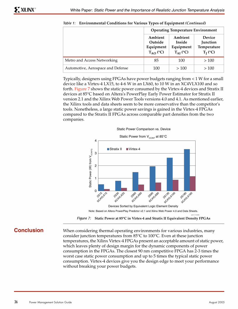
White Paper: Static Power and the Importance of Realistic Junction Temperature AnalysisR
Typically, designers using FPGAs have power budgets ranging from < 1 W for a small device like a Virtex-4 LX15, to 4-6 W in an LX60, to 10 W in an XC4VLX100 and so forth. Figure 7 shows the static power consumed by the Virtex-4 devices and Stratix II devices at 85°C based on Altera's PowerPlay Early Power Estimator for Stratix II version 2.1 and the Xilinx Web Power Tools versions 4.0 and 4.1. As mentioned earlier,the Xilinx tools and data sheets seem to be more conservative than the competitor's tools. Nonetheless, a large static power savings is gained in the Virtex-4 FPGAs compared to the Stratix II FPGAs across comparable part densities from the two companies.
Conclusion When considering thermal operating environments for various industries, many consider junction temperatures from 85°C to 100°C. Even at these junction temperatures, the Xilinx Virtex-4 FPGAs present an acceptable amount of static power,which leaves plenty of design margin for the dynamic components of power consumption in the FPGAs. The closest 90 nm competitive FPGA has 2-3 times theworst case static power consumption and up to 5 times the typical static power consumption. Virtex-4 devices give you the design edge to meet your performance without breaking your power budgets.
Metro and Access Networking 85 100 > 100
Automotive, Aerospace and Defense 100 > 100 > 100
Figure 7: Static Power at 85°C in Virtex-4 and Stratix II Equivalent Density FPGAs
Table 1: Environmental Conditions for Various Types of Equipment (Continued)
Operating Temperature Environment
Ambient Outside
Equipment TAO (°C)
AmbientInside
EquipmentTAI (°C)
Device Junction
TemperatureTJ (°C)
2S15
XC4VLX
152S
30
XC4VLX
252S
60
XC4VLX
602S
90
XC4VLX
80
2S13
0
XC4VLX
100
2S18
0
XC4VLX
160
Stratix II Virtex-4
Static Power Comparison vs. Device
Note: Based on Altera PowerPlay Predictor v2.1 and Xilinx Web Power 4.0 and Data Sheets.
Static Power from VCCINT at 85°C
Devices Sorted by Equivalent Logic Element Density
Sta
tic P
ower
(W
) fr
om V
CC
INT
Q
4
3
2
0
1
wp221_07_032305
36 Power Management Solution Guide August 2005
August 2005 Power Management Solution Guide 37
© 2005 Xilinx, Inc. All rights reserved. All Xilinx trademarks, registered trademarks, patents, and further disclaimers are as listed at http://www.xilinx.com/legal.htm. All other trademarks and registered trademarks are the property of their respective owners. All specifications are subject to change without notice.
NOTICE OF DISCLAIMER: Xilinx is providing this design, code, or information "as is." By providing the design, code, or information as one possible implementation of this feature,application, or standard, Xilinx makes no representation that this implementation is free from any claims of infringement. You are responsible for obtaining any rights you may require for your implementation. Xilinx expressly disclaims any warranty whatsoever with respect to the adequacy of the implementation, including but not limited to any warranties or representations that this implementation is free from claims of infringement and any implied warranties of merchantability or fitness for a particular purpose.
Summary This application note describes how to implement the CoolRunner™-II advanced features in the Xilinx software. These features include the DualEDGE triggered registers, clock divider,CoolCLOCK, DataGATE, Schmitt trigger inputs, and I/O termination types. HDL code examples are available for download, see Code Examples Download, page 9.
CoolRunner-II Xilinx CoolRunner-II CPLDs combine performance and low power in a single device. For more information on the architecture of CoolRunner-II CPLDs, see References, page 10. CoolRunner-II CPLDs feature enhanced clocking flexibility and provide design capabilities that significantly reduce power consumption.All design features discussed in this application note are supported in Foundation™ ISE™ and WebPACK™ ISE software from Xilinx. For more information on Xilinx software, see References, page 10.
Software Attributes
There are two main methods of attribute entry, each with their own advantages. A UserConstraint File (UCF) has the advantage of being easily edited while being separate from the design source files. It has the benefit of allowing changes without needing to re-synthesize thesource code. For more information on entering constraints with the UCF, see References, page 10.Attribute entry within the source has the advantage of not needing to maintain a separate file for the design constraints. All CoolRunner-II VHDL and Verilog attribute examples are only applicable to the XST synthesis tool.The attributes that are user definable and specific to the CoolRunner-II CPLD include: CoolCLOCK, DataGATE, Schmitt trigger input, keeper or pullup I/O termination, I/O standards, VREF, and open drain outputs. Some design constraints from this list are software selectable via the ISE Project Navigator GUI. Individual signal constraints must be explicity defined in the methods described above.Please note that several syntax and help guides for attributes exist within the Xilinx ISE Project Navigator. These help files are updated with each release of software and provide a reliable source of information. The help menu can be located from within ISE under the menu option Help | ISE Help Contents | CPLD Attributes.
DualEDGE Registers
CoolRunner-II DualEDGE triggered registers allows designers to reach unprecedentedperformance levels. CoolRunner-II CPLDs can double system performance by creatingDualEDGE triggered (DET) registers. CoolRunner-II DET registers allow data to be registeredon both the rising and falling edge of a clock.CoolRunner-II DET registers can be used for logic functions that include shift registers, counters,comparators, and state machines. Designers must evaluate the desired performance of the CPLD logic to determine use of DET registers.The DET register can be inferred in any ABEL, HDL, or schematic design. Table 1 lists the inference methods available to create a DET register in CoolRunner-II.
Application Note: CoolRunner-II
XAPP378 (v1.2) June 5, 2005
Using CoolRunner-II Advanced FeaturesR
Table 1: DET Register Inference SummaryDesign Entry Instantiation Method
ABEL Use the following syntax:QOUT:=data; QOUT.DEC=clock;
VHDL/Verilog Infer a dual edge triggered register.
Schematic Instantiate a FDDn[S][R][E] component.

38 Power Management Solution Guide August 2005
Using CoolRunner-II Advanced FeaturesR
ExamplesA designer can infer a single edge triggered (SET) register in any HDL design. A SET registeractive on the rising edge of the input clock would require the following VHDL or Verilog syntax.VHDL: if (clock’event) and (clock = ’1’) thenVerilog: always @ (posedge clock)
The required syntax to infer a CoolRunner-II DET register requires the register be active on boththe rising and falling edge of the clock. The following VHDL syntax would be used to infer a CoolRunner DET register.process (clock)beginif (clock’event) then...
end if;end process;
The following Verilog syntax would be used to infer a DET register in CoolRunner-II.always @ (negedge clock or posedge clock)...
The DET register is available with all macrocells in all devices of the CoolRunner-II family.
Clock Divider CoolRunner-II CPLDs provide additional clocking flexibility to the DET register feature with the clock divider. The CoolRunner-II clock divider provides the capability to divide an incoming clock and globally distribute the divided clock to all macrocells. The clock divider provides additional power savings by reducing the toggle frequency of the internal clock network.The CoolRunner-II clock divider is available on global clock, GCK2, and can divide the incomingclock by 2, 4, 6, 8, 10, 12, 14, and 16. The clock divider creates a 50-50 duty cycle divided clock without affecting TCO. The clock divider output is initialized low by the CPLD power up reset circuitry.The clock divider circuit includes an active high synchronous reset, referred to as CDRST. Whenthe CDRST signal is asserted, the clock divider output is disabled after the current cycle. When the CDRST signal is de-asserted the clock divider output will become active upon the first edge of GCK2. Figure 1 illustrates the CoolRunner-II clock divider.
The CoolRunner-II clock divider includes a built in delay circuit. With the delay feature enabled, the output of the clock divider will be delayed for one full count cycle. When used, the clock divider does not output a rising clock edge until after the divider reaches the terminal count value. The delay feature is either enabled or disabled upon configuration. The type of clock divider component instantiated will determine if the delay is enabled or disabled. Figure 2 illustrates a timing waveformof the CoolRunner-II clock divider with the delay enabled and disabled.
Figure 1: CoolRunner-II Clock Divider
Figure 2: Clock Divider Waveform
Global
Clock
(GCK2)
CDRST
Clock
Divide
By
2,4,6,…,16
DIV2
DIV4
DIV16
to FB 1
to FB n
x378_01_041202
1st
GCK2
CDRST
Divide by 2
Divide by 16
Divide by 2
Divide by 16
No
Delay
3rd 5th 7th 17th
Clock Cycles
Delay
Enabled
x378_02_050802
August 2005 Power Management Solution Guide 39
Using CoolRunner-II Advanced FeaturesR
Xilinx Synthesis Technology (XST) allows a clock divider component to be instantiated directly in the HDL source code. Table 2 lists the available clock divider components that can be instantiated in any ABEL, HDL, or schematic design.
VHDL ExampleTo design with the CoolRunner-II clock divider in VHDL requires both a component declaration and component instantiation. The component declaration declares the name and interface of the clock divider unit. The VHDL component declaration syntax for using a clock divide by 2, the CLK_DIV2 component is shown here.component CLK_DIV2 isport (CLKIN : in STD_LOGIC;CLKDV : out STD_LOGIC );
end component;
The component instantiation associates signals with the ports of the clock divider component. If a clock divide by 2 is desired, the CLK_DIV2 component must be instantiated. The incoming clock signal, clk, is declared on the CLKIN port and the clock divider output signal, clk_div_by_2, is declared on the CLKDV output port. The VHDL syntax is shown here for instantiating the CLK_DIV2 component.U1: CLK_DIV2port map(CLKIN => clk,CLKDV => clk_div_by_2 );
If a clock divide by 16 with a synchronous reset and start delay is desired, the CLK_DIV16RSD component must be declared and instantiated. The VHDL syntax for the component declaration is shown here.component CLK_DIV16RSD isport (CLKIN : in STD_LOGIC;CDRST : in STD_LOGIC;CLKDV : out STD_LOGIC );
end component;
The component instantiation assigns the port signals. The input clock signal, clk, is declared on the CLKIN port. The clock divider reset signal, clk_div_rst, is declared on the CDRST port. The clockdivider output, clk_div_by_16, is declared on the CLKDV port. This component will also enable the start delay circuitry in the CoolRunner-II clock divider. The syntax to instantiate the CLK_DIV16RSD component in VHDL is shown here.U1: CLK_DIV16RSD port map (CLKIN => clk, CDRST => clk_div_rst, CLKDV => clk_div_by_16 );
Verilog ExampleVerilog design entry with XST does not require a component declaration; only the component instantiation is necessary. The Verilog syntax to instantiate the CLK_DIV16RSD component is
Table 2: Clock Divider Library ComponentsComponent DescriptionCLK_DIVn Global Clock Divider Component. No support of the synchronous reset or
start delay features.Available: CLK_DIV2, 4, 6, 8, 10, 12, 14, 16
CLK_DIVnR Global Clock Divider with Synchronous Reset. No support of the start delay feature.Available: CLK_DIV2, 4, 6, 8, 10, 12, 14, 16R
CLK_DIVnSD Global Clock Divider with Start Delay. No support of the synchronous reset.Available: CLK_DIV2, 4, 6, 8, 10, 12, 14, 16SD
CLK_DIVnRSD Global Clock Divider with Synchronous Reset and Start Delay.Available: CLK_DIV2, 4, 6, 8, 10, 12, 14, 16RSD

40 Power Management Solution Guide August 2005
Using CoolRunner-II Advanced FeaturesR
shown here. The input clock signal, clk, is assigned to the CLKIN port. The clock divider reset signal, clk_div_rst, is assigned to the CDRST port. The clock divider output, clk_div_by_16, is assigned to the CLKDV port.CLK_DIV16RSD U1 (.CLKIN (clk),.CDRST (clk_div_rst),.CLKDV (clk_div_by_16) );
ABEL ExampleDesigning with clock dividers in CoolRunner-II requires both the component declaration and component instantiation. The clock divider must be declared as an external component in an ABEL design as shown here.CLK_DIV2R external (CLKIN, CDRST -> CLKDV);
Component instantiation in an ABEL design occurs by assigning an identifier to the clock divider component. In this example, U1 is the identier assigned to the clock divider component,CLK_DIV2R, using the functional_block ABEL keyword.U1 functional_block CLK_DIV2R;
The following equations illustrate the component port mapping. The input clock, clk, is mapped tothe CLKIN port. The clock divider reset signal, clk_div_rst, is mapped to the CDRST port. The clock divider output signal, clk_div_by_2, is assigned to the CLKDV output port.U1.CLKIN = clk;U1.CDRST = clk_div_rst;clk_div_by_2 = U1.CLKDV;
Notes: 1. The signal assigned to the CDRST port will automatically be mapped to the CDRST/I/O pin.2. The output of the clock divider circuit is only available as a clock input to registers within the CPLD.
The clock divider output can not be used in combinational logic or routed off-chip for external use.3. The clock divider is available on CoolRunner-II 128 macrocell devices and larger.
CoolCLOCK The CoolRunner-II CoolCLOCK feature is the technique of combining the global clock dividerand DET registers. Power savings are achieved by dividing the global clock by 2, distributing a lower frequency clock on the internal clock network, and then doubling the clock at eachmacrocell. Zero clock skew can be acheived due to the zero insertion delay of the clock dividerand the DET registers. Figure 3 illustrates the CoolRunner-II CoolCLOCK feature.
Since GCK2 is the only clock network that can be divided, the CoolCLOCK feature is only available on GCK2. The CoolCLOCK feature can be implemented by assigning an attribute to an input
Figure 3: CoolCLOCK
Input
Divide
Clock
Device
Routing Macrocell
GCK2
CDRST
DIV2
Divide
by 2
D/T/LQ
T
Latch
DualEDGE
D
Global
Divided
Clock
x378_03_041202

August 2005 Power Management Solution Guide 41
Using CoolRunner-II Advanced FeaturesR
clock. The CoolCLOCK attribute replaces the need to instantiate the clock divider and infer DETregisters. Table 3 lists the methods available to use the CoolCLOCK attribute..
Note: The CoolCLOCK feature is available on CoolRunner-II 128 macrocell devices and larger.
DataGATE CoolRunner-II designers can block specified inputs under the control of the DataGATE function.By blocking inputs, switching signals do not drive internal chip capacitance and thereby reduce overall power consumption. The last value on the input pin prior to the assertion of theDataGATE rail is latched and used by the CPLD internally. Figure 4 illustrates the DataGATEfeature in CoolRunner-II.
There are two attributes associated with the DataGATE feature in CoolRunner-II. The first attribute specifies if an input will be affected by DataGATE and the second designates the DataGATE control signal.The DataGATE feature is selectable on a per pin basis. Each input pin that uses DataGATE must be assigned a DATA_GATE attribute. Table 4 illustrates the syntax for enabling DataGATE on an input signal.
The DataGATE assertion rail can be driven from either an I/O pin or internal logic. The DataGATE enable signal is a dedicated DGE/I/O pin for each package in CoolRunner-II. Upon implementation, the software recongnizes a design using DataGATE and automatically assigns this I/O pin to the DataGATE enable control function, DGE. Internally generated DataGATE contol
Table 3: CoolCLOCK AttributeAttributeFormat Syntax Example
UCF NET <clock name> COOL_CLK; NET clk COOL_CLK;
ABEL XILINX PROPERTY 'COOL_CLK <clock name>'; XILINX PROPERTY ’COOL_CLK clk’;
VHDL attribute COOL_CLK : string;attribute COOL_CLK of <clock name>: signal is "TRUE";
attribute COOL_CLK : string;attribute COOL_CLK of clk : signal is "TRUE";
Verilog //SYNTHESIS attribute COOL_CLK of <clock name>: signal is "TRUE";Note: The comment delimiters are intentional andnecessary for XST.
//SYNTHESIS attribute COOL_CLK of clk : signal is "TRUE";
Figure 4: DataGATE Block Diagram
Data Latch
to AIM
DataGATE
Assertion Rail
Input
Pin
Configuration
Bit
X378_04_041202
Table 4: DataGate AttributeAttributeFormat Syntax Example
UCF NET <signal name> DATA_GATE; NET data_in DATA_GATE;
ABEL XILINX PROPERTY 'DATA_GATE <signal name>'; XILINX PROPERTY ’DATA_GATE data_in’;
VHDL attribute DATA_GATE : STRING;attribute DATA_GATE of <signal name>: signal is "TRUE";Note: The string attribute need only be declared once for all DATA_GATE attributes.
attribute DATA_GATE : STRING;attribute DATA_GATE of data_in : signal is "TRUE";
Verilog //SYNTHESIS attribute DATA_GATE of <signal name>: signal is "TRUE";Note: The comment delimiters are intentional andnecessary for XST.
//SYNTHESIS attribute DATA_GATE of data_in : signal is "TRUE";

42 Power Management Solution Guide August 2005
Using CoolRunner-II Advanced FeaturesR
logic can be assigned to this I/O pin with the BUFG=DATA_GATE attribute. The methods of assigning the DataGATE enable signal are shown in Table 5.
Schmitt Trigger Each CoolRunner-II I/O has multiple input buffers used for various I/O standard configurations.One of these input buffers behaves as a Schmitt trigger input and is enabled upon CPLD configuration. The Schmitt trigger input allows the board designer the flexibility to utilize the CoolRunner-II with both high speed signals as well as slow switching signals on the same device. Slowly switching signals can cause havoc on digital systems by causing doubleclocking or glitches on a CMOS input, however this can be virtually eliminated by using theSchmitt trigger input. The Schmitt trigger input use is only at the cost of a few nanosecond delay (refer to the CoolRunner-II datasheet, see References, page 10).Table 6 illustrates the attribute syntax to assign the Schmitt trigger input buffer to a specific signal..
I/O Termination CoolRunner-II pins may be terminated in the following ways: keeper (also referred to as bushold) and pullup. Usage of the keeper and the pullup circuitry is exclusive on a global basis.When one of these two (keeper and pullup) termination modes is selected for any number ofsignals, the other termination mode is no longer available to any other signal.
KeeperThe keeper circuitry provides the ability to hold the last known value on an I/O pin using weak pullup/down resistors. If an unterminated I/O pin was in high-impedence and floating, this would cause excessive leakage current. The keeper circuitry eliminates the need for external termination
Table 5: DataGate Control AttributeAttributeFormat Syntax Example
UCF NET <signal name> BUFG=DATA_GATE; NET dg_en BUFG=DATA_GATE;
ABEL XILINX PROPERTY 'BUFG=DATA_GATE <signal name>';
XILINX PROPERTY ’BUFG=DATA_GATE dg_en’;
VHDL attribute BUFG : STRING;attribute BUFG of <signal name>: signal is "DATA_GATE";Note: The string attribute need only be declared oncefor all BUFG attributes.
attribute BUFG : STRING;attribute BUFG of dg_en : signal is "DATA_GATE";
Verilog //SYNTHESIS attribute BUFG of <signal name>: signal is "DATA_GATE";Note: The comment delimiters are intentional andnecessary for XST.
//SYNTHESIS attribute BUFG of dg_en : signal is "DATA_GATE";
Table 6: Schmitt Trigger AttributeAttributeFormat Syntax Example
UCF NET <signal name> SCHMITT_TRIGGER; NET data_in SCHMITT_TRIGGER;NET clock SCHMITT_TRIGGER;
ABEL XILINX PROPERTY 'SCHMITT_TRIGGER<signal name>';
XILINX PROPERTY 'SCHMITT_TRIGGER data_in';XILINX PROPERTY 'SCHMITT_TRIGGER clock';
VHDL attribute SCHMITT_TRIGGER : STRING;attribute SCHMITT_TRIGGER of <signal name>: signal is "TRUE";Note: The string attribute need only be declaredonce for all SCHMITT_TRIGGER attributes.
attribute SCHMITT_TRIGGER : STRING;attribute SCHMITT_TRIGGER of data_in: signal is "TRUE";attribute SCHMITT_TRIGGER of clock: signal is "TRUE";
Verilog //SYNTHESIS attribute SCHMITT_TRIGGER of <signal name>;Note: The comment delimiters are intentional andnecessary for XST.
//SYNTHESIS attribute SCHMITT_TRIGGER of data_in;//SYNTHESIS attribute SCHMITT_TRIGGER of clock;

August 2005 Power Management Solution Guide 43
Using CoolRunner-II Advanced FeaturesR
that would resolve this. Table 7 illustrates the attribute syntax for specifying the keeper termination on any I/O pin.
PullupThe internal pullup allows the designer to eliminate external pullup resistors on the board, thereby reducing cost and simplifying board layout. Table 8 illustrates the attribute syntax for specifying the pullup I/O termination.
I/O Configuration
CoolRunner-II devices support multiple I/O banks in a single device, allowing for easy interfacing to different voltage standards on one chip. A device can support one I/O standardper bank (i.e., XC2C128 has two banks and can therefore support up to two I/O standards).Regardless of which I/O voltage standard is selected, any pin may be configured as an open-drain output.
I/O StandardsTable 9 lists the supported I/O standards on CoolRunner-II devices. Note that all standards are notsupported in every density.
Table 7: Keeper AttributeAttributeFormat Syntax Example
UCF NET <signal name> KEEPER; NET data_in KEEPER;NET clock KEEPER;
ABEL XILINX PROPERTY 'KEEPER <signal name>'; XILINX PROPERTY 'KEEPER data_in';XILINX PROPERTY 'KEEPER clock';
VHDL attribute KEEPER : STRING;attribute KEEPER of <signal name>: signal is "TRUE";Note: The string attribute need only be declared once for all KEEPER attributes.
attribute KEEPER : STRING;attribute KEEPER of data_in: signal is "TRUE";attribute KEEPER of clock: signal is "TRUE";
Verilog //SYNTHESIS attribute KEEPER of <signal name>;Note: The comment delimiters are intentional andnecessary for XST.
//SYNTHESIS attribute KEEPER of data_in;//SYNTHESIS attribute KEEPER of clock;
Table 8: Pullup AttributeAttributeFormat Syntax Example
UCF NET <signal name> PULLUP; NET data_in PULLUP;NET clock PULLUP;
ABEL XILINX PROPERTY 'PULLUP <signal name>'; XILINX PROPERTY 'PULLUP data_in';XILINX PROPERTY 'PULLUP clock';
VHDL attribute PULLUP : STRING;attribute PULLUP of <signal name>: signal is "TRUE";Note: The string attribute need only be declared once forall PULLUP attributes.
attribute PULLUP : STRING;attribute PULLUP of data_in: signal is "TRUE";attribute PULLUP of clock: signal is "TRUE";
Verilog //SYNTHESIS attribute PULLUP of <signal name>;Note: The comment delimiters are intentional andnecessary for XST.
//SYNTHESIS attribute PULLUP of data_in;//SYNTHESIS attribute PULLUP of clock;
Table 9: CoolRunner-II Supported I/O StandardsXC2C32A XC2C64A XC2C128 XC2C256 XC2C384 XC2C512
I/O Banks 2 2 2 2 4 4
LVTTL Yes Yes Yes Yes Yes Yes
LVCMOS33,LVCMOS25,
& LVCMOS18
Yes Yes Yes Yes Yes Yes

44 Power Management Solution Guide August 2005
Using CoolRunner-II Advanced FeaturesR
Figure 5 illustrates how to specify the default I/O standard for all pins in a design. The I/O standard can be selected in the Implement Design Process Properties window under the Basic Tab.
If a design requires multiple I/O standards on the same device, each pin must be manually declared with the appropriate I/O standard attribute. Table 10 illustrates the available I/O standard attributes that can be declared.
1.5V I/Os Yes Yes Yes Yes Yes Yes
SSTL2-1 & SSTL3-1
No No Yes Yes Yes Yes
HSTL-1 No No Yes Yes Yes Yes
Figure 5: Global I/O Standard Selection
Table 10: I/O Standard AttributesI/O Standard Attribute Name
LVTTL LVTTL
LVCMOS 3.3V LVCMOS33
LVCMOS 2.5V LVCMOS25
LVCMOS 1.8V LVCMOS18
1.5V I/O LVCMOS15
Table 9: CoolRunner-II Supported I/O StandardsXC2C32A XC2C64A XC2C128 XC2C256 XC2C384 XC2C512
August 2005 Power Management Solution Guide 45
Using CoolRunner-II Advanced FeaturesR
Table 11 illustrates the syntax for specifying an I/O standard attribute. The examples shown in Table 11 are for specifying the LVCMOS18 I/O standard. For other standards, LVCMOS18 can be replaced with the appropriate attribute name shown in Table 10.
Open DrainA signal that is grounded when "false" and is in high-impedence when "true" is considered an open-drain signal. An output on CoolRunner-II can be configured as open drain by simply declaring the OPEN_DRAIN attribute in the Xilinx software. Table 12 illustrates the syntax for specifing an open drain output with the OPEN_DRAIN attribute.
Code Examples Download
Example source code is available for download. Both VHDL and Verilog code with test benches are available for using the CoolRunner-II advanced features.THE DESIGNS ARE PROVIDED TO YOU "AS IS". XILINX MAKES AND YOU RECEIVE NO WARRANTIES OR CONDITIONS, EXPRESS, IMPLIED, STATUTORY OR OTHERWISE, AND XILINX SPECIFICALLY DISCLAIMS ANY IMPLIED WARRANTIES OF MERCHANTABILITY,NON-INFRINGEMENT, OR FITNESS FOR A PARTICULAR PURPOSE. These are only example designs, not fully functional cores. XILINX does not warrant the performance, functionality, or operation of these designs will meet your requirements, or that the operation of the designs will be uninterrupted or error free, or that defects in the designs will be corrected. Furthermore, XILINX
SSTL 2-1 SSTL2_I
SSTL 3-1 SSTL3_I
HSTL-1 HSTL_I
Table 10: I/O Standard AttributesI/O Standard Attribute Name
Table 11: I/O Standard Attribute SyntaxAttributeFormat Syntax Example
UCF NET <signal name> <I/O standard attributename>;
NET data_in IOSTANDARD=LVCMOS18;NET clock IOSTANDARD=LVCMOS18;
ABEL XILINX PROPERTY 'IOSTANDARD=LVCMOS18 <signal name>';
XILINX PROPERTY 'IOSTANDARD=LVCMOS18 data_in';XILINX PROPERTY 'IOSTANDARD=LVCMOS18 clock';
VHDL attribute IOSTANDARD : STRING;attribute IOSTANDARD of <signal name>: signal is "<I/O standard attribute name>";Note: The string attribute need only be declaredonce for all IOSTANDARD attributes.
attribute IOSTANDARD : STRING;attribute IOSTANDARD of data_in: signal is "LVCMOS18";attribute IOSTANDARD of clock: signal is "LVCMOS18";
Verilog //SYNTHESIS attribute IOSTANDARD of <signal name> is "<I/O standard attribute name>";Note: The comment delimiters are intentional and necessary for XST.
//SYNTHESIS attribute IOSTANDARD of data_in is "LVCMOS18";//SYNTHESIS attribute IOSTANDARD of clock is "LVCMOS18";
Table 12: Open Drain AttributeAttributeFormat Syntax Example
UCF NET <signal name> OPEN_DRAIN; NET data_out OPEN_DRAIN;
ABEL XILINX PROPERTY 'OPEN_DRAIN <signal name>'; XILINX PROPERTY 'OPEN_DRAIN data_out';
VHDL attribute OPEN_DRAIN : STRING;attribute OPEN_DRAIN of <signal name>: signal is "TRUE";Note: The string attribute need only be declared oncefor all OPEN_DRAIN attributes.
attribute OPEN_DRAIN : STRING;attribute OPEN_DRAIN of data_out: signal is "TRUE";
Verilog //SYNTHESIS attribute OPEN_DRAIN of <signal name>;Note: The comment delimiters are intentional andnecessary for XST.
//SYNTHESIS attribute OPEN_DRAIN of data_out;

46 Power Management Solution Guide August 2005
Using CoolRunner-II Advanced FeaturesR
does not warrant or make any representations regarding use or the results of the use of the designs in terms of correctness, accuracy, reliability or otherwise.XAPP378 - http://www.xilinx.com/products/xaw/coolvhdlq.htm
Conclusion Performance and low power have finally come together with CoolRunner-II CPLDs. The available advanced features furthur reduce power consumption and provide advanced clockingmanagement options. For additional assistance with the CoolRunner-II advanced features,please contact the Xilinx hotline or refer to the Xilinx web support (http://support.xilinx.com/).
References 1. CoolRunner-II family data sheet2. CoolRunner-II Application Notes3. Xilinx ISE design entry software4. Application Note: XAPP352: Utilizing a UCF for CoolRunner XPLA3 CPLDs

August 2005 Power Management Solution Guide 47
© 2002 Xilinx, Inc. All rights reserved. All Xilinx trademarks, registered trademarks, patents, and further disclaimers are as listed at http://www.xilinx.com/legal.htm. All other trademarks and registered trademarks are the property of their respective owners. All specifications are subject to change without notice.
NOTICE OF DISCLAIMER: Xilinx is providing this design, code, or information "as is." By providing the design, code, or information as one possible implementation of this feature,application, or standard, Xilinx makes no representation that this implementation is free from any claims of infringement. You are responsible for obtaining any rights you may require for your implementation. Xilinx expressly disclaims any warranty whatsoever with respect to the adequacy of the implementation, including but not limited to any warranties or representations that this implementation is free from claims of infringement and any implied warranties of merchantability or fitness for a particular purpose.
Summary CoolRunner™-II CPLDs are the only CPLD to combine both high performance and low powerto form the next generation CPLD. This application note describes the design methodologiesthat can be employed to obtain the lowest power possible using the CoolRunner-II CPLD byutilizing its unique power saving features.
Introduction CoolRunner-II CPLDs continue to employ the features of Fast Zero Power (FZP) technology as found in the earlier CoolRunner CPLD generations. But due to unique Xilinx design techniques,smaller geometries, and state of the art process technology, FZP technology has furtheradvanced CoolRunner-II CPLDs as the low power standard. Other CPLD manufacturers haveattempted to reproduce the FZP true CMOS technology of the CoolRunner CPLDs, but havenot been able to meet the CoolRunner benchmark. For the first time in the CPLD industry,CoolRunner-II devices deliver both true high performance and low power at the same time,along with the lowest standby current in the industry without the use of power down modes. Inaddition, these devices offer unique power saving features such as CoolCLOCK, DataGATE, and DualEDGE flip-flops.
Traditional CPLDs use sense amp type product terms to provide fast propagation delay times.Sense amp product terms are biased in a manner to detect a small change in voltage levels onthe word line which indicates a change in the logic state of the product term. The transistorbiasing constantly draws current, even at standby. With this in mind, these types of CPLDs cannot provide a low power solution, as can CoolRunner-II CPLDs. As sense amp type devicesizes become larger in macrocell count, power grows significantly since there are many moreproduct terms to consume power.
As process technology shrinks, sense amp type CPLDs will inherently consume more power to maintain performance. Smaller process technology demands lower power supply voltages thereby reducing the gain of the sense amp. Further, product term transistors leak more withthe smaller geometries. To maintain performance, a sense amp CPLD will need to be designed such that its biasing compensates for the leakage and boosts gain to detect the smaller voltageswing of the word line. Higher biasing will cause more current to flow through the bias network, thereby increasing total power consumption. Other CPLD manufacturers that use sense ampbased technology will inevitably go through a learning process to re-design their current products to compensate for the effect of ever shrinking process technology.
CMOS product terms, as used in the FZP technology, inherently consume less power when not switching states. Since CMOS logic exhibits low standby current, CoolRunner-II CPLDs use this technology to reap the benefits of low power. Additionally, CMOS technology benefits from smaller geometries where the device consumes less power and becomes faster.
Power SavingFeatures
New architectural features have been added to the CoolRunner-II product line to enhance the power saving capabilities of the FZP technology. This section describes these features and how they can be used to save power.
All new features described below are available with the XC2C128 and larger devices. The smaller devices, XC2C32 and XC2C64, do not include some features, specifically DataGATE, Clock Divider, and CoolCLOCK.
Application Note: CoolRunner-II CPLD
XAPP377 (v1.0) May 8, 2002
Low Power Design with CoolRunner-II CPLDs
R

48 Power Management Solution Guide August 2005
Low Power Design with CoolRunner-II CPLDsR
DataGATEMany times devices are connected to a data bus which are not being addressed by the masterdevice. When a CPLD is in this situation, it will use more power than necessary since the data on the bus is not useful to the CPLD, but the data lines continue to toggle, which subsequently toggles the internal logic of the CPLD. Any logic that changes state within the CPLD will consume power. Therefore, it follows that disconnecting the CPLD from the data bus when the device is not addressed conserves power, as highlighted in this example.
DataGATE solves this issue by disconnecting external signal activity from the internal logic,consequently reducing power consumption of the device. This is achieved by using a unique,software enabled, CoolRunner-II pass gate at the I/O pin (when configured as an input) whichis controlled by the DataGATE global net. This control net originates from a specific pin/macrocell and can be driven by either an external signal or an internally developed signal using logic elements. When the pass gate on the input pin is disabled by the DataGATE control net, an internal latch drives the CPLD logic network maintaining the same logic level that was present on the input pin just prior to asserting the DataGATE control net. This preserves thecurrent logic state internal to the CPLD while external data changes states.
For example, a CoolRunner-II CPLD that shares a data bus with other devices will most likelyhave its own address and typically will not be addressed continuously. Two options exist to disconnect the data bus from the CoolRunner-II CPLD when not addressed. First, if the device is addressed using a chip select signal, this signal can be assigned to the DataGATE control pin and used to isolate the inputs from the data bus. Second, if using an address bus, the address of the device can be decoded internally to the CPLD which can then be used to enable, viaDataGATE, the data bus inputs to receive data when addressed. When the CPLD is not addressed, DataGATE would disconnect the external data bus signals using address decoding internally to the CPLD. In this case, the result of the internal decoding is routed to the DataGATE pin to disconnect the toggling bus.
DataGATE can be configured to affect any or all I/O pins, with the exception of JTAG pins and the DataGATE pin itself. The above example discusses DataGATE configured to affect a few macrocell I/O pins. It may be beneficial in other applications to disconnect the system clock orclocks from the CPLD. The two elements that consume the most power are output buffers andthe clock tree. If the CPLD is not needed for a specific amount of time, the DataGATE feature could be used to gate the clock. Doing so will dramatically reduce power consumption. However, caution must be exercised when gating a clock since undesired logic transitions may occur.
There are other cases where the unique CoolRunner-II DataGATE feature is useful to reducepower. Also, DataGATE is flexible such that the entire device or only parts of the device can be isolated from external signals, depending on the application. For example, it can be used in CoolRunner-II CPLDs to enhance board troubleshooting procedures.
Schmitt TriggerCoolRunner-II Schmitt trigger inputs are useful for applications that require hysteresis on the inputs. A useful application might be where noise is an issue on specific pins. Hysteresis provides added noise immunity. Another application could implement an oscillator circuit which is constructed external to the CPLD, but CPLD logic is used to implement portions of the oscillator circuit.
To ensure the lowest power consumption in the CoolRunner-II CPLDs, disable the Schmitttrigger inputs since these types of buffers consume more power than the regular input buffer. Itis important to design and operate the system in a low noise environment when Schmitt triggers are disabled to prevent inadvertent transitions on the CPLD inputs.
Clock DividerGlobal clock networks tend to be the largest power consuming elements in CPLDs. Any effortto reduce the frequency of the global clock network greatly benefits the system with respect topower consumption. Therefore, CoolRunner-II devices have been designed to include a clock divider network on global clock, GCK2. Without introducing additional clock delays, the clock

August 2005 Power Management Solution Guide 49
Low Power Design with CoolRunner-II CPLDsR
divider has the capability of dividing the system clock by even integers ranging from 2 to 16, as shown in Figure 1.
Some systems use state machines, for example, that do not require the full speed of theexternal system clock. A clock divider is the perfect tool to reduce system power in this case.The clock divider provides an excellent alternative to adding a user defined clock divider built from logic, which would waste logic otherwise usable for more features in the design. A lower frequency on the global clock network, provided by the clock divider, will reduce the power consumed by the CoolRunner-II CPLD.
Generally speaking, designing with the slowest system clock possible will reduce power consumption. To this end, the clock divider provided in the CoolRunner-II architecture will greatly assist the designer.
DualEDGE RegistersBy utilizing both edges of the clock signal, the macrocell can do twice the work when configured as a DualEDGE flip-flop. Figure 2 displays the macrocell configured as a DualEDGE flip-flop. A system without the aid of the DualEDGE flip-flop would need to provide a clock at twice thefrequency to obtain the same work output at the macrocell. Since the macrocells with DualEDGE flip-flops operate on both the rising and falling edges of the clock, the clock networkis used more efficiently. Consequently, power consumption is reduced when the global clock net is operating at a lower frequency.
DualEDGE flip-flops further enhance the functional possibilities of the clock divider andtherefore improve power savings. The global clock can be effectively divided by odd integers of3, 5, and 7 if used with the DualEDGE flip-flop. For example, if a divide by 3 clock is desired for the design, the Clock Divider can be set to a divide by 6 and then effectively doubled by the DualEDGE flip-flop resulting in a divide by 3 characteristic. This is important to note since,again, lower clock frequencies always save power. The DualEDGE flip-flop effectively adds more functionality to the clock divider network.
Perhaps the design contains two state machines. One state machine can efficiently operate at1/4th the system clock frequency, yet the other state machine can much more efficiently operate at 1/8th the system clock frequency. DualEDGE flip-flops can be employed in conjunction with the clock divider to obtain such a scenario. The state machine running at 1/8th
Figure 1: Clock Division Circuitry for GCK2
Figure 2: Macrocell Clock Chain with DualEDGE Option Shown
X377_01_041102
ClockIn
¸2¸4¸6¸8
¸10¸12¸14¸16
GCK2
CDRST
Synch Rst
GCK0GCK1GCK2CTC
PTC
PTCx377_02_041102
D/T
CE
CK
FIFLatchDualEDGE
Q

50 Power Management Solution Guide August 2005
Low Power Design with CoolRunner-II CPLDsR
the system clock frequency can simply use the clock divider configured as divide by 8. Enabling the DualEDGE flip-flop on macrocells assigned to the other state machine and assigning the divide by 8 clock divider to those macrocells as well will yield an effective clock frequency that is 1/4th the system clock frequency. This means that the single clock divider can obtain virtual dual functionality of a divide by 8 and a divide by 4 counter. Notice that both clocks aresynchronized with each other and the system clock so that the two state machines operateconcurrently.
Summarizing the previous discussion, when utilizing the CoolRunner-II clock divider and/or the DualEDGE flip-flops, it is possible to obtain clock divisors of 2, 3, 4, 5, 6, 7, 8, 10, 12, 14 and 16.Additionally, when a group of macrocells use the clock divider and some of those macrocells use DualEDGE flip-flops, the clock divider network can effectively deliver two clock frequenciesof divisors 1-2 (using CoolCLOCK described later), 2-4, 3-6, 4-8, 5-10, 6-12, 7-14, and 8-16.When DualEDGE flip-flops are used with the clock divider, lower power is achieved while more efficiently operating the design.
CoolCLOCKCoolRunner-II CPLDs are equipped with a unique feature, CoolCLOCK, to further reduce the power consumption of the global clock network without affecting the speed of the clock. Notethat CoolCLOCK does not impose additional clock delays. As explained earlier, any efforts toreduce the clock frequency of the global clock net will significantly reduce power consumption.
CoolCLOCK reduces power consumed by the global clock net by dividing the external clockfrequency by 2 before it is applied to the global clock network. This clock division occurs early in the clock tree near the clock input buffer so that the divided clock affects the majority of the clock network. Since the global clock network contains a relatively large amount of internalcapacitance, a slower frequency will significantly reduce power consumed by this net, GCK2. This divided clock signal is then effectively doubled at the macrocell using the DualEDGEclocking feature of the flip-flops in the macrocell, shown in Figure 3. This ensures that the original clock frequency is applied to the macrocell as intended by the external system. Only macrocells that require the original clock frequency will be configured to utilize the DualEDGE flip-flop feature. Other macrocells can be configured to use the divided clock frequency tofurther reduce power when those macrocells don’t require clocking at full speed.
Figure 3: CoolCLOCK Created by Cascading Clock Divider and DualEDGE Option
GCK0GCK1GCK2CTC
PTC
PTC
X377_03_041102
D/T
CE
CK
FIFLatchDualEDGE
Q
ClockIn
÷2÷4÷6÷8
÷10÷12÷14÷16
GCK2
Synch Reset
Synch Rst

August 2005 Power Management Solution Guide 51
Low Power Design with CoolRunner-II CPLDsR
Weak Pull-up and Bus HoldAll CoolRunner-II CPLDs include I/O termination options to reduce power consumption of the I/O due to externally 3-stated busses. The I/O termination circuitry can be configured in three ways: weak pull-up, bus hold, and no termination. Pull-up and bus hold are selected on a global basis and are mutually exclusive. Subsequently, the use or absence of the selected termination is specified on a per pin basis. Weak pull-up connects a high-impedance resistive load onto theI/O pin to prevent a floating situation on the pin. Bus hold is essentially a full latch on the I/O pinwhich drives the last state present on the I/O, either High or Low, prior to the bus going to the high impedance state. Bus hold is referred to in the software as "Keeper".
Floating inputs, an input which is not driven to a High or Low logic state, can use excessive power since the voltage on the gate of the input buffer may wander to a voltage level between standard logic levels. In this case, the input buffer is driven into the linear region where the P and N channel transistors are both switched on. Therefore, to avoid this situation, I/Os can beconfigured to use internal pull-ups or bus hold circuitry. I/Os configured as inputs orbidirectional should utilize this feature if it is known that the bus to which the I/O is attached will float at some point in its regular operation.
There are some cases where weak pull-up is undesirable. If the bus is pulled down the majorityof time, current will flow through the weak pull-up to ground via the buffer, pulling the bus Low.A design such as this would benefit by using the bus hold circuitry.
A rule of thumb for any CMOS device is to not allow inputs to float. These two features ofCoolRunner-II CPLDs, weak pull-up and bus hold, will minimize the chance of consuming excessive power on input pins.
I/O termination should be considered for each application and each I/O to determine the best combination to reduce power consumption. Again, avoid floating inputs whenever possible.
Slew RateThis is a feature of the I/O structure that regulates the rate at which the output buffer changesstates. There are two modes: FAST and SLOW. Designers concerned with reducing reflections on circuit board traces, minimizing RFI or minimizing EMI should specify a SLOW slew rate.Most design engineers considering low power designs will usually be designing slower speed systems and therefore will not be as concerned with reflections. In a case such as this, the system will benefit from a lower power perspective when slew rate is specified to be FAST.
Although an I/O is configured as an output, the input buffer is still connected to the pin and therefore senses changes in voltage on that pin. If the output is configured with a SLOW slewrate, the output voltage switches states less quickly, thereby lingering longer between standard logic levels. The input buffer will therefore be driven in the linear region (the input voltage between standard logic levels) for a longer period of time than if the output was configured in the FAST slew rate mode. Current will flow through the input buffer P and N channel transistors for a longer period of time resulting in higher power consumption. It is therefore recommended to configure the output with a FAST slew rate whenever reflections are not a concern.
Power SavingTechniques
Several rules of thumb should be followed when designing any circuit with CMOS devices toreduce power consumption. A basic understanding of power consumption must be reachedprior to discussing these rules of thumb. Therefore, a derivation of the current equation forCMOS devices is necessary. Once the mathematical model of current is understood, itbecomes easy to follow the theory of the rules of thumb. To maximize power savings, the designer should apply these concepts when implementing any CMOS device.
Derivation of Current Equation in CMOS DevicesSince the CMOS device is constructed of PMOS and NMOS transistors, the dynamic model is simply a capacitive structure for each transistor. Of course, the basic structure of a capacitor is the dielectric between two plates. In this case, the dielectric of the capacitor is the oxide layer on the silicon wafer and the plates are the poly or metal gate together with the inversion layer in the channel. The interconnecting metal/poly routing is also modeled as a capacitor where the plates are the routing itself together with any underlying routing or conductive material and the dielectric is any non-conductive structure between the plates. With these capacitive structures,

52 Power Management Solution Guide August 2005
Low Power Design with CoolRunner-II CPLDsR
the CMOS device is largely modeled as a collection of capacitors. Recall the basic equation for current through a capacitor:
Breaking the derivative into its components we can extract the basic equation for frequency,which is the inverted value of a change in time, and simplify the equation:
Since the voltage for capacitive structures in CMOS devices changes as a square wave withdiscontinuities between logic HighHigh and Low and is ideally rail to rail, we can further simplifythe equation. For example, in a system of supply voltage, V, the change in voltage, dV, is V to0V as shown and reduced here:
Therefore the current equation for each capacitive structure becomes:
where:
• I = current in Amperes
• C = the capacitance of the capacitive structure in Farads
• V = the system voltage in Volts
• f = the toggle frequency of the capacitive structure in Hz
Dynamic device current is the summation of all capacitive structures toggling over time. Voltage remains the same for all equations and can be assumed to be a constant. A device of n capacitive structures can be represented as follows:
To obtain total device current, static current must be added to the dynamic current:
For illustrational purposes, it may be easier to discuss total current using a simplified version of this equation:
where:
• ICC = total device current in Amperes
• ICCQ = quiescent device current in Amperes
• C = the lumped capacitance of the device in Farads
• V = the system voltage in Volts
• f = the average device toggle frequency in Hz
Recall that to obtain power, multiply current by voltage to yield Watts.
I Ctd
dV=
I C Vd1
td---- =
I C Vd f =
Vd V2
V1
–=
Vd V 0–=
Vd V=
I C V f =
IDynamic
V Ci
i 1=
n
fi
=
ITotal
IStatic
V+ Ci
i 1=
n
fi
=
ICC
ICCQ
C+ V f =

August 2005 Power Management Solution Guide 53
Low Power Design with CoolRunner-II CPLDsR
Reduce System SpeedIt becomes obvious from the equation that for a fixed device capacitance and voltage, reducing the average device toggle rate will reduce power consumption.
Limiting the system clock speed as well as the data bus speed to slower values will reducepower consumption since average device toggle rate will become smaller. Careful analysis of the required CPLD clock speed is essential for low power design. Over-clocking the CPLD design beyond the needs of the logic unnecessarily consumes extra power. Evaluating theminimum required speed of the CPLD logic will ensure that the system clock will have a minimal effect on power consumption.
Drive Inputs to Standard Logic LevelsPower consumption will rise dramatically when a CMOS input buffer is not driven to known, standard logic levels, otherwise known as allowing the input to "float". A voltage level between standard logic levels causes the input buffer transistors, typically P and N channel, to be biasedin a manner where both are in the ON state. When biased in this way, a large amount of current will flow between the power and ground supplies of the device via this channel. It is therefore imperative to drive the input buffer to a known logic level High or Low state to turn off one ofthese two transistors and avoid this situation.
The beauty of CMOS logic is that power consumption is nearly zero when logic gates are held at a known logic input level. FZP technology found in CoolRunner-II CPLDs uses this principle to provide dramatic power savings over other CPLDs.
Further, it is advised to drive the input to the full voltage rail on a High logic level and fully to ground on a logic Low level. Even though the voltage level is within the acceptable logic levels, i.e., VIH and VIL, the closer the voltage is to the absolute voltage rails, the less current will be consumed in the input buffer. This effect is much less than the scenario where the input voltage floats between logic levels, but nevertheless can have a significant impact on total power consumption when summed across several I/Os.
Increase Input Edge SpeedCMOS device inputs that are driven by a slowly switching source will consume more power since the input spends more time biased in the linear region. Again, the linear region is found when an input is biased at a voltage between standard logic High or Low levels. When theCMOS input buffer is biased in this manner, both the P and N channel transistors are turned on, allowing a relatively large amount of current to pass to ground. The longer the buffer is biasedin this fashion, the more power will be consumed by the device. Therefore, it is recommended to quickly switch the signal as it is applied to the inputs of the CMOS device. This applies to all clock pins, dedicated input pins, or I/Os configured as inputs or bidirectional.
Eliminate Bus ConflictsOccasionally, bus conflicts occur where two output buffers are driving a line at the same time in opposite directions. This adversely affects logic performance as well as power consumption.Two drivers attempting to swing the bus at opposite voltage levels will draw excessive current.
A similar situation occurs when a bus is pulled High via a pull-up resistor, for example, and the output buffer is driving the bus Low. In this example, current will flow from the power source,through the pull-up resistor, the N channel transistor in the output buffer, and to ground.Current, in this case, is a function of the value of the pull-up resistor and the N channel impedance. A weak pull-up resistor, on the order of 10k ohms or more, is a good place to startif it is desired to use such a component. The larger the resistor, the less power will be consumed, but this will slow down the bus response time when the resistor is required to charge the bus to the High level if the bus is in the 3-state condition.
It is recommended to continuously drive a bus line High or Low with one device at a time andremove pull-up resistors whenever possible to obtain the lowest power condition. In somesituations, this may not be possible. For example, an SMBus or I2C SDA line is required to bereleased by all components but be at a High level when released. In this case, a pull-up resistoris required.

54 Power Management Solution Guide August 2005
Low Power Design with CoolRunner-II CPLDsR
Bus TerminationsA different case where pull down resistors are necessary is when shunt bus termination is required to reduce reflections in high speed designs. These terminations are usually designedto be pull down resistors whose value equals the equivalent impedance of the data bus transmission line and are positioned as close to the load pin as possible. Whenever the outputbuffer is driving a transmission line with shunt resistors, the P channel transistor will source current into the load and therefore will raise power consumption.
It may be possible to avoid using shunt termination resistors by using a very short transmissionline. The rule of thumb for a short transmission line is one whose length is less than one-sixththe electrical length of the rise time, and is described using the following equation:
where:
• Length = maximum line length in inches
• Trise = rise time in seconds
• L = the line inductance in Henries/inch
• C = the line capacitance in Farads/inch
By using the CoolRunner-II CPLD slew rate feature configured to SLOW, the rise time becomes longer. Using the above equation, it can be determined if the length of the transmission line can be effectively long enough to avoid reflections altogether. If by using the SLOW slew ratefeature, the length of the transmission line is short by the above rule of thumb, shunt bus termination resistors can be avoided thereby saving power.
If either method is not an option, insert a series termination resistor positioned at the source pin with the same value as the transmission line impedance. This option will avoid excessive power consumption (since there is no shunt load) and eliminate reflections at the source. However, aseries termination resistor will allow one reflection at the load (since the load impedance doesnot match the transmission line impedance) which implies that any component mid way between the source and the load will see two transitions: the incident wave and the single reflected wave created at the load.
Reduce System VoltageUsing the total current equation with fixed capacitance and average frequency, it becomes readily apparent that reducing system voltage will reduce power consumption, provided the system voltage remains within recommended operating specifications. Therefore, it makes sense to use a 1.8V device in lieu of a 3.3V or 2.5V device. CoolRunner-II CPLDs are 1.8V devices and therefore utilize this concept. Further, a device made with a smaller process technology, such as CoolRunner-II CPLDs, will generally have lower lumped internal capacitance values thereby reaching additional power savings. Combining these two factors with reducing average system frequency will also cut power consumption.
With any voltage device, there is a recommended operating range, and it may be advantageous to operate low in that voltage range to further reduce power consumption. Voltages that areoutside the recommended operating range may cause excessive power consumption including adverse functional performance.
Reduce Bus LoadingConnecting an external bus to a CMOS device will increase power consumption due to the loading effects of the bus on the device. The primary factor from loading is given by capacitive or resistive bus components as seen by the output buffer looking into the bus.
Capacitive loading comes in two forms: lumped and distributed. Lumped capacitance is typically found from the gate of the input buffer of other connected CMOS devices. It is also developed from any capacitive element that is attached to the bus. Distributed capacitance is present due to the routing of the trace on the PCB. Both types will charge and discharge during logic transitions based on the previous logic state of the bus. Capacitive loading will drawcurrent from the CMOS device whose output buffer is driving the bus, thereby increasing apparent power consumption of that device as seen at its power pins. To minimize power
Length1
6---
Trise
LC
------------«

August 2005 Power Management Solution Guide 55
Low Power Design with CoolRunner-II CPLDsR
consumption based on this capacitive loading effect, it is necessary to reduce the size of thelumped capacitance found in attached devices, and to shorten the PCB traces. Doing so will also increase potential system speed since reflections are less likely.
Resistive loading is usually found when devices with a resistive element to their impedance is attached to the bus. For example, a pull down resistor attached to a PCB trace will allow for current to flow from the CMOS device power rail, through the P channel of the output buffertransistor, through the resistor, and to ground, increasing observed power consumption at the CMOS device power pins. Reducing resistive loads will reduce power consumption.
Keep in mind that many components are comprised of more than one type of impedance element. For example, capacitors also have resistive and inductive elements, albeit small.
Further Power Saving TechniquesFor further discussions regarding power saving techniques, particularly those involving logic design, review XAPP346 - Low Power Tips for CoolRunner Design found at http://www.xilinx.com/xapp/xapp346.pdf. Although the referenced application note discusses CoolRunner XPLA3 CPLDs, the basic principles apply to CoolRunner-II CPLDs.
Conclusion For the first time in the CPLD industry, CoolRunner-II products combine true high speed logic with ultra low power. Unique features of the CoolRunner-II CPLD, such as CoolCLOCK and DataGATE, allow the designer to further reduce power consumption. By using these features combined with good design practice, as outlined in this document, designers can be assured that their design will experience optimal low power benefits without sacrificing high speed.
References 1. Johnson H. and Martin G. (1993): High-Speed Digital Design: A Handbook of Black Magic Prentice Hall PTR

56 Power Management Solution Guide August 2005
© 2003 Xilinx, Inc. All rights reserved. All Xilinx trademarks, registered trademarks, patents, and further disclaimers are as listed at http://www.xilinx.com/legal.htm. All other trademarks and registered trademarks are the property of their respective owners. All specifications are subject to change without notice.
NOTICE OF DISCLAIMER: Xilinx is providing this design, code, or information "as is." By providing the design, code, or information as one possible implementation of this feature,application, or standard, Xilinx makes no representation that this implementation is free from any claims of infringement. You are responsible for obtaining any rights you may require for your implementation. Xilinx expressly disclaims any warranty whatsoever with respect to the adequacy of the implementation, including but not limited to any warranties or representations that this implementation is free from claims of infringement and any implied warranties of merchantability or fitness for a particular purpose.
Summary This application note outlines the various ways designers can utilize the DataGATE feature of CoolRunner™-II CPLDs.
Introduction CoolRunner-II CPLDs deliver the lowest power consumption in today’s CPLD marketplace.Built from standard CMOS structures, they achieve the classic ICC = CVF relationship where “C” is driven capacitance, “V” is voltage swing and “F” is the switching frequency of gates drivenwithin the part. The capacitance and voltage values in the equation are essentially demanded by the 0.18 micron process, but the “F” part of the expression is due to the designcharacteristics of the customer design inside. The desire to lower the “F” aspect resulted in the DataGATE feature in CoolRunner-II CPLDs.As the name implies, the feature “gates” data. This application note shows how to get as nearto the origin of the ICC versus “F” curve as we can with today’s technology. It describes thepractical aspects of how DataGATE works, the timing model, and what you will need to do in the software to make it work. Further, it shows four different ways the circuitry can be used for power reduction, as well as for circuit debugging, printed circuit board “hot plugging,” and device security. These are just some ideas on how to use this feature, and others may come tomind as users learn to operate DataGATE.The final section of this application note lists additional application notes which cover otheraspects of Xilinx CoolRunner-II CPLDs.
Operation Figure 1 details the delivery of the DataGATE Assertion Rail throughout the I/O structure of a CoolRunner-II CPLD. This image doesn’t convey the generation of the DataGATE activationmethod, but simply the delivery of the control signal to each input pin, with independent control of whether that pin will participate in the gating action. Specifically, two items should be noted. First, each pin can be programmed to participate in the DataGATE operation or not—thestandard default is not to participate. The second aspect is that the individual pass transistors permit signal entry into the CPLD, or blocking of the input pin. Figure 2 expands the detail for a single input pin. If the input pin becomes blocked, the last driven value into the CPLD will automatically be latched and held so a solid binary value is delivered into the CPLD core. Itshould be noted that the Assertion Rail is driven from a specific macrocell within the CPLD, and that when that macrocell drives high, input data will be blocked at participating pins. If the Assertion Rail is low, data passes freely into the chip. The condition of the DataGATEAssertion Rail is manifested at a specific pin (designated DGE), which will vary from chip to chip within the CoolRunner-II family.
Application Note: CoolRunner-II CPLDs
XAPP395 (v1.2) September 22, 2003
Using DataGATE in CoolRunner-II CPLDsR

August 2005 Power Management Solution Guide 57
Using DataGATE in CoolRunner-II CPLDsR
Figure 3 details the timing action of the DataGATE operation. Specifically, the DataGATE Enable pin, if driven from an external pin, can be viewed as a clocking type function. Given that,it has standard clock type timing parameters, a setup time (TDGSU), hold time (TDGH), a minimum width (TDGW) and DataGATE recovery time (TDGR). For clarity, Figure 3 also showsthe propagation time (TPD) from input to output of a simple signal. DataGATE operation is described in detail in XAPP378, which describes how to declare the appropriate conditions in ABEL, VHDL and Verilog. DataGATE pin participation is also described, so you can easily dictate which pins will participate in the operation.
Figure 1: DataGATE Assertion Rail
Figure 2: DataGATE Assertion Rail Input Pin, Latching Old State
Figure 3: DataGATE Timing Parameters
Latch
to AIM
Latch
to AIM
Latch
to AIM
Latch
to AIM
Latch
to AIM
MC16
PLA
AIM
MC2MC1
MC16
PLA
MC2MC1
MC16
PLA
MC2MC1
MC16
PLA
MC2MC1
DataGATE Assertion Rail
XAPP_01_032503
ConfigurationBit
Data Latch
to AIM
DataGATEAssertion Rail
InputPin
XAPP_02_032503
DataGATE Enable
Data at Pin
Output Data at Pin
TPD TDGR
TDGWTDGHTDGSU
TPD
Application Note: CoolRunner-II CPLDs

58 Power Management Solution Guide August 2005
Using DataGATE in CoolRunner-II CPLDsR
Applications Simple Power savingFigure 4 shows the simplest DataGATE configuration, and possibly the most frequently usedmethod. Here, a simple external signal is delivered on a pin to the CPLD, which connects thatsignal through the Advanced Interconnect Matrix (AIM) to the DataGATE macrocell. TheDataGATE macrocell is a specific macrocell in each part, which can drive the assertion rail. The logic created at the macrocell is arbitrary, so for this example, we can assume it is a simpleconnection. Hence, when the external pin drives high, that signal drives the Assertion Rail high. When the external pin drives low, so goes the Assertion Rail. As discussed earlier, when driven low, participating and nonparticipating input pins will have their signals forwarded into the CPLD. When driven high, participating input pins will be blocked and latched, while nonparticipating pins will still pass their signals into the CPLD. It is possible for all input pins to be “gated,” so care should be used in choosing signals. Blocking clocks typically has thehighest payoff, but also the highest risk. Figure 4 shows the case where an external conditiondecides when to save power.
Timer Figure 5 expands on the idea of Figure 4, including a timeout circuit (timer) that is employed todrive the Assertion Rail whenever the timeout signal asserts. We can assume that the timer delivers a “0” when the timer is counting clocks, but when it hits a previously chosen timeoutperiod, it asserts a logical "1" and drives the blocking signal to the Assertion Rail. Becausemost timers are fairly simple counters, and frequently, it is not important to be too fussy about exactly which count value is chosen (ie, plus or minus a clock or two won’t matter), it may besmart to pick the simplest logic structure that can solve the timer problem. In all likelihood, this will be a Linear Feedback Shift Register (LFSR), which will produce most of the values of a binary counter, but in a non-consecutive order and with minimum logic beyond the macrocell flip flops. By either "And"ing the appropriate state, or choosing a state variable for directconnection to the Assertion Rail, the timer can drive the Assertion Rail as needed.
Figure 4: Simple External DataGATE Control Signal
Figure 5: DataGATE Under Control of Internal Timer
Signal drives lowto pass data
DataGATE
Assertion
Rail
AIM
External signaldrives high to enable data flow
XAPP_04_032503
Signal drives lowto pass data
DataGATE
Assertion
Rail
External clock to internal timer
TIMER
Application Note: CoolRunner-II CPLDs

August 2005 Power Management Solution Guide 59
Using DataGATE in CoolRunner-II CPLDsR
It would also be possible to use the timer circuit to lock out signals that are deemed to beinfrequently used, but periodically “wake up” to sample the pins for whatever reason that might be needed. Alternately, selected signals simply become permanently blocked at the completion of a timeout period. Another view would not have the counter counting “time,” butrather some other number of events that drive the “timer” clock input site—say, count 400interrupt signals then block this set of pins.
ControllerAs suggested earlier, any logic can be constructed to drive the Assertion Rail, so statemachines can be created, too. In this sense, external variables can be combined with state variables to create the condition that drives the rail. As described with the timer, externalsignals can create a tally that is used to power down, but also, combinations of events andstates can create the blocking event. Figure 6 shows the insertion of an arbitrary controllermodule, which includes flip flops and logic to interact with the external signals and clocks.
Another important point to consider when using DataGATE is the overall time operation of a system. At initial power-on, certain actions occur in many systems—processor bootstrap,memory initialization, memory space and I/O space definition, etc. After these initial activities, many items remain in their initial condition and stay there throughout the operation. If certain registers or logic are only used at the beginning, but free running strobe signals, clocks, or datacontinue unnecessary switching, then those logic sections might benefit from “DataGating.”
Debugging with DataGATE
Latching the input pins when the Assertion Rail blocks inputs creates an additional capability: an on-chip debugger. Logic analyzers typically capture the contents of binary signals—the“state”—by triggering on an event, then snapshotting the data into a memory buffer for later readback. Combining the previously described controller with the JTAG circuitry inherent in aCoolRunner-II permits a simpler, but effective capability. For instance, assume that most of the pins are participating in the DataGATE operation. Assume next that we wish to isolate the state of the CPLD when a certain combination of inputs and internal CPLD states occurs—say an“error” state. By creating a state machine out of scrap gates and flops within the CPLD, the inputs can be blocked and held until the JTAG circuit reads back the entire state of the CPLD for dissection and analysis with a PC and JTAG cable. Alternately, the triggering event of a logic
Figure 6: DataGATE Rail Driven by Internal State Machine Controller
Signal drives lowto pass data
DataGATEAssertion
RailExternal clock
Deb
ug T
rigge
r
Signal A
Signal B
Debug Trigger InputsXAPP_06_032503
Application Note: CoolRunner-II CPLDs

60 Power Management Solution Guide August 2005
Using DataGATE in CoolRunner-II CPLDsR
analyzer can be taken over to the CPLD and applied just as in the first, simple “power saving” model described above. Figure 7 gives some detail on how this might occur.
This model of debugging is one way to use the input latches on the CPLD, although others viewthis as a very large set of input latches that can be controlled for simple data capture at the pins.The only drawback to this is that the timing for the data capture tends to increase on the largerparts, so users should plan for a little extra time delay.
Hot Plugging with DataGATE
Hot Plugging, Hot Socketing and Live Insertion are all terms that are used interchangeably. The standard situation is this: there is a rack of equipment that is powered up, and a user needs toinsert a board into that rack without turning the power off. The methodology for this is somewhat nebulous because expectations vary widely between engineers: depending on how much they know about the situation, engineers all expect different behavior . Some expect theboard insertion to go perfectly, without any control signals being disturbed or data bits beingdropped. Others expect the board insertion to result in possible data corruption, but not in any catastrophic crashing of the systems. Experienced designers cross their fingers and are satisfied if the event doesn’t result in the rack catching on fire.
A user’s expectation should be that there will be no actual damage, but that extra care must be taken to prevent corrupt behavior. For instance, all the devices on the “cold board” areuncharged where most of the elements within the “hot” rack are charged up (bus lines,decoupling capacitors, whatever). Inserting a discharged board presents a substantial capacitive load to a system that has finite charge on it. This will require charging the “cold”board to the appropriate level before operation can occur. One solution to this has been the “extended finger” method whereby little extension tabs are placed on the cold board, soelectricity is delivered to the board before the logic enters the rack connectors; however, this
Figure 7: Debugging with DataGATE
Signal drives lowto pass data
DataGATEAssertion
RailExternal clock
Deb
ug T
rigge
r
Signal A
Signal B
Debug Trigger InputsXAPP_06_032503
Application Note: CoolRunner-II CPLDs
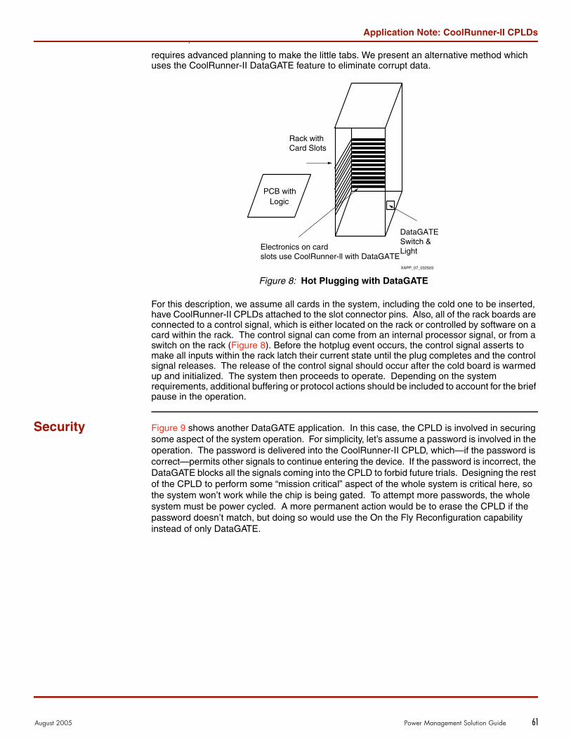
August 2005 Power Management Solution Guide 61
Using DataGATE in CoolRunner-II CPLDsR
requires advanced planning to make the little tabs. We present an alternative method which uses the CoolRunner-II DataGATE feature to eliminate corrupt data.
For this description, we assume all cards in the system, including the cold one to be inserted,have CoolRunner-II CPLDs attached to the slot connector pins. Also, all of the rack boards are connected to a control signal, which is either located on the rack or controlled by software on a card within the rack. The control signal can come from an internal processor signal, or from aswitch on the rack (Figure 8). Before the hotplug event occurs, the control signal asserts tomake all inputs within the rack latch their current state until the plug completes and the control signal releases. The release of the control signal should occur after the cold board is warmedup and initialized. The system then proceeds to operate. Depending on the systemrequirements, additional buffering or protocol actions should be included to account for the brief pause in the operation.
Security Figure 9 shows another DataGATE application. In this case, the CPLD is involved in securing some aspect of the system operation. For simplicity, let’s assume a password is involved in the operation. The password is delivered into the CoolRunner-II CPLD, which—if the password is correct—permits other signals to continue entering the device. If the password is incorrect, the DataGATE blocks all the signals coming into the CPLD to forbid future trials. Designing the rest of the CPLD to perform some “mission critical” aspect of the whole system is critical here, sothe system won’t work while the chip is being gated. To attempt more passwords, the whole system must be power cycled. A more permanent action would be to erase the CPLD if the password doesn’t match, but doing so would use the On the Fly Reconfiguration capability instead of only DataGATE.
Figure 8: Hot Plugging with DataGATE
PCB withLogic
Rack withCard Slots
Electronics on cardslots use CoolRunner-ll with DataGATE
DataGATESwitch &Light
XAPP_07_032503
Application Note: CoolRunner-II CPLDs

62 Power Management Solution Guide August 2005
Using DataGATE in CoolRunner-II CPLDsR
Conclusions DataGATE is a versatile and helpful feature designers can utilize when designing with CoolRunner-II CPLDs, although they are not required to use it and it can be used only overchosen pins, as needed.
A simple strategy for using DataGATE is to design with no initial regard for it, except in saving the macrocell that drives the assertion rail. Once the design is complete, evaluate the current drawn against the target current budget. Next, consider implementing CoolClock or other power savings options. Again, evaluate consumed current against target current. ReviewXAPP 377 for other things to try.Next, if the design does not hit its target, or you simply wish to see how low the current can betaken, then consider using DataGATE. Consider sections of your design that initially “wake up” and perform active behavior, then go “quiet” for the rest of the operation. Assuming they aredriven from active pins, can you identify some time or event that would permit them to be blocked by the DataGATE circuit? If so, define the time or event, create a logic circuit tomanifest at that time and have it drive the DataGATE rail. Evaluate the current again. If you need less current, can you include more pins? Can you slightly change the block point (in time) to include more pins? If so, alter your design and re-evaluate. Should you encounter a “tweak” that adversely affects your design, you can back up a revision to the last working one and knowthat it is better than your original solution.
Further Reading Application Noteshttp://www.xilinx.com/xapp/xapp375.pdf (Timing Model)http://www.xilinx.com/xapp/xapp376.pdf (Logic Engine)http://www.xilinx.com/xapp/xapp377.pdf (Low Power Design)http://www.xilinx.com/xapp/xapp378.pdf (Advanced Features)http://www.xilinx.com/xapp/xapp379.pdf (High Speed Design)http://www.xilinx.com/xapp/xapp380.pdf (Cross Point Switch)http://www.xilinx.com/xapp/xapp381.pdf (Demo Board)http://www.xilinx.com/xapp/xapp382.pdf (I/O Characteristics)http://www.xilinx.com/xapp/xapp383.pdf (Single Error Correction Double Error Detection)http://www.xilinx.com/xapp/xapp384.pdf (DDR SDRAM Interface)http://www.xilinx.com/xapp/xapp387.pdf (PicoBlaze Microcontroller)http://www.xilinx.com/xapp/xapp388.pdf (On the Fly Reconfiguration)http://www.xilinx.com/xapp/xapp389.pdf (Powering CoolRunner-II CPLDs)http://www.xilinx.com/xapp/xapp393.pdf (8051 Microcontroller Interface)http://www.xilinx.com/xapp/xapp394.pdf (Interfacing with Mobile SDRAM)
Figure 9: DataGATE Dynamic Security
Signal drives lowto pass data
DataGATEAssertion
RailExternal clock
Pas
swor
d C
heck
er
Password
PW Strobe
Security InputsXAPP_08_032503
Application Note: CoolRunner-II CPLDs

August 2005 Power Management Solution Guide 63
Using DataGATE in CoolRunner-II CPLDsR
CoolRunner-II Data Sheets http://direct.xilinx.com/bvdocs/publications/ds090.pdf (CoolRunner-II Family Datasheet)http://direct.xilinx.com/bvdocs/publications/ds091.pdf (XC2C32 Datasheet)http://direct.xilinx.com/bvdocs/publications/ds092.pdf (XC2C64 Datasheet)http://direct.xilinx.com/bvdocs/publications/ds093.pdf (XC2C128 Datasheet)http://direct.xilinx.com/bvdocs/publications/ds094.pdf (XC2C256 Datasheet)http://direct.xilinx.com/bvdocs/publications/ds095.pdf (XC2C384 Datasheet)http://direct.xilinx.com/bvdocs/publications/ds096.pdf (XC2C512 Datasheet)
CoolRunner-II White Papershttp://www.xilinx.com/publications/products/cool2/wp_pdf/wp165.pdf (Chip ScalePackaging)http://www.xilinx.com/publications/whitepapers/wp_pdf/wp170.pdf (Security)
Application Note: CoolRunner-II CPLDs

64 Power Management Solution Guide August 2005
© 2005 Xilinx, Inc. All rights reserved. All Xilinx trademarks, registered trademarks, patents, and further disclaimers are as listed at http://www.xilinx.com/legal.htm. All othertrademarks and registered trademarks are the property of their respective owners. All specifications are subject to change without notice.
NOTICE OF DISCLAIMER: Xilinx is providing this design, code, or information "as is." By providing the design, code, or information as one possible implementation of this feature,application, or standard, Xilinx makes no representation that this implementation is free from any claims of infringement. You are responsible for obtaining any rights you may require for your implementation. Xilinx expressly disclaims any warranty whatsoever with respect to the adequacy of the implementation, including but not limited to any warranties or representations that this implementation is free from claims of infringement and any implied warranties of merchantability or fitness for a particular purpose.
Summary This application note demonstrates how multiple devices, including VirtexTM-II, SpartanTM-3, and Spartan-3L FPGAs, can be effectively power managed by a single CoolRunnerTM-II CPLD. It is written with battery powered applications in mind.
Introduction All chips draw power, but some applications are more sensitive than others to the amountdrawn. Portable applications are sensitive simply because they draw from a battery. Most digital chips are designed to operate at 5V, 3.3V, 2.5V, 1.8V, and so forth. This does not match well with today’s battery voltages. Hence, there will be a regulator or two on most boards. Managing power will involve managing those regulators.
CoolRunner-II CPLDs were designed to operate with a core voltage of 1.8V, well suited to its 0.18 micron core, but its I/O structure supports 3.3V, 2.5V, 1.8V, and 1.5V operation. Being standard low power CMOS, the I/Os also operate within that range, but are only speed specified at those voltages.
CoolRunner-II CPLDs have been successfully used as voltage translators, logic collection sites and even power management solutions. Their “early on” behavior makes them ideal for managing other chips’ power. This application note focuses on using CoolRunner-II to manage power for Xilinx FPGAs, providing greater FPGA utility in a portable products. Additional CoolRunner-II qualities are shown to add value to reducing the portable product power budget in many cases.
The Power Equation
As expected, the starting point is physics, but CMOS power consumption can be deceptive.Simplistically, it follows an equation relating the switching speed of a logic gate output, times thevoltage range over which it swings, times the load capacitance being driven. Adding in the static leakage component says it all.
Equation 1: Power = V(VCF) + static power
where:
V = output voltage swing
C = load capacitance
F = gate output switching frequency
Static power = somewhat constant value for many parts (often negligible)
This equation is a guideline. Originally developed for a simple CMOS inverter, it shows a trend, but only suggests how to reduce power. Equation 1 drives most CMOS power estimation tools.Xilinx provides several ways to estimate power, including spreadsheets, application notes and the XPower software, available with the ISE™ design suite.
Application Note: CPLD
XAPP436 (v1.1) March 30, 2005
Managing Power with CoolRunner-II CPLDs
R

August 2005 Power Management Solution Guide 65
The CoolRunner-II SolutionR
The CoolRunner-II Solution
The CoolRunner-II approach to power management attacks both static and dynamic current. A battery is a charge reservoir with varying capabilities on voltage regulation, and in some cases an ability to be recharged. Each battery has its own qualities for delivering charge. Manybatteries can deliver high currents for brief time periods, or smaller currents for longer times.Trade-offs can and must be made.
To get a feeling for power activity, let’s look at a real world example, that was documented byPortelligent in their Report #116.02- 031023-1d. Figure 1 is a reconstruction of theirmeasurements made on an LG cell phone that was able to record video or take a picture.Figure 1 shows power use while taking a photograph, with the cell phone camera.
The steps in taking a still photo are summarized as:
1. Power up and turn on the LCD backlight2. Select the camera from menu3. Select taking a still photo4. Take the photo5. Return to the main menu6. Power down
The numbers in the diagram correspond to the activity list above. The Portelligent reportexplains the activity of the various chips within the camera, but Figure 1 shows the composite power. There are many variables at play. Several chips within the camera receive power atdifferent times. The display, camera chip and memories are involved here, but none of the standard cell phone capabilities - like making a call. That requires a different profile. Nonetheless, these actions are typical of a large number of today’s portable systems ranging from, walkie-talkies to PDAs, to video cameras, to the emerging software defined radios (SDR).3G cell phones, in particular, with their added on applications and multi-band operation takethis type of power management to new heights. In fact, these systems may rival some of the very power conscious projects like the Mars rover or other deep space probes in complexity.Power management is vital to all of these products.
Now, let’s shift our attention to Figure 2 which shows a small system using two FPGAs, anASSP and a CoolRunner-II CPLD. Note, there are also multiple regulator chips shown (LDO), deriving their voltages by regulating down 5 volts. Another approach would be to regulate downfrom a battery, which most regulators can manage.
This particular example has the FPGAs being powered through the LDOs, but the ASSP simply connects to the distributed supply through a power FET. The particular FET will depend on the channel drop that can be tolerated, the turn on voltage and the power requirements of the ASSP. All power sources are controlled from logic signals coming off CoolRunner-II pins. The idea here is simple. When CoolRunner-II remains turned on, its power consumption is only in microamps (standby), whereas the FPGA current ranges into milliamps, depending on family and density.
Figure 1: Power Profile of LG Cell Phone Taking Still Photograph
2.5
1.5
0.5
0
1
2W
atts
0 20 40
Seconds
60 80 100
1
2 3
45
6
XAPP436_01101304
Application Note: CPLD

66 Power Management Solution Guide August 2005
The CoolRunner-II SolutionR
In this example, we have combined a 150 nanometer Virtex-II FPGA and a 90 nanometer Spartan-3 FPGA. Each has different power needs, and illustrates choices and trade-offs to be made. As we will see later, the CoolRunner-II will be able to introduce an extra power down mode to the FPGAs, to reduce dynamic power. That will give a choice on whether to turn the part off, and pay for reconfiguration again, or just reduce dynamic power during standard operation. A reasonable regulator for the LDO 2 module is the TPS5003 from Texas InstrumentsTM.
The Virtex-II FPGA has reduced power up surge, but larger density parts may draw morecurrent than a portable budget allows. Each FPGA might be a candidate for shutdown, exceptwhen needed. Table 1 summarizes quiescent internal current drawn by various Virtex-II family members. The dynamic current is a function of signal switching rates within the parts, and is design dependent. To estimate the power, you can use any of the methods mentioned earlier,or simply build up the design and measure the requirement. Additional estimation resources are listed at the end. Table 2 gives similar data for Spartan-3 FPGAs.
Figure 2: Multiple Chips “Power Managed” by a CoolRunner-II CPLD
Table 1: Virtex-II FPGA Typical Internal Quiescent Currents
Virtex-II Device Typical Internal Quiescent Supply Current(1)
XC2V40 3 mA
XC2V80 5 mA
XC2V250 8 mA
XC2V500 10 mA
XC2V1000 12 mA1. Refer to the data sheet for the most accurate and up-to-date information
ASSP
LDO1
LDO2
LDO3
EN
EN3
5 Volts
1.8V
1.5V
3.3VEN1EN2
2.5V1.2V
CoolRunner-IICPLD
Spartan-3
Virtex-II
Table 2: Spartan-3/L FPGA Typical Internal Quiescent Currents
Spartan-3/L DeviceSpartan-3 Typical Internal
Quiescent Supply Current(1)Spartan-3L Typical InternalQuiescent Supply Current(1)
Spartan-3L Quiescent(1)
Max (Hibernate Mode)(2)
XC3S50 10 mA
XC3S200 20 mA
XC3S400 35 mA
XC3S1000/L 65 mA 30 mA 6 mA
XC3S1500/L 65 mA 50 mA 8 mA1. Refer to the data sheet for the most accurate and up-to-date information2. Hibernate Mode available for Spartan-3L. See DS313.
Application Note: CPLD

August 2005 Power Management Solution Guide 67
The CoolRunner-II SolutionR
Figure 3 shows how a current profile might look (averaged) over time. Usually, there is an initial surge as all on board capacitance becomes charged, various parts undergo configuration,initialization, bootstrapping, and so forth. Then things settle down, and various chips can beturned off, placed into low power, or whatever, as dictated by the application. The average current draw of this profile is substantially less than the initial surge value, so there may be apayoff for turning chips off all together, or placing them in a low power mode. Table 3 and Table 4 give configuration times in byte wide mode at maximum speed.
By lowering the average power, CoolRunner-II CPLDs can dramatically extend the battery life of a system in a way that brings the high flexibility and value of FPGAs into the portable world. Let’s show how more value is gained using CoolRunner-II DataGATE.
Figure 3: Current Profile of a System with Various Active Devices Over Time
Table 3: Virtex-II Configuration Parameters
Virtex-II Device Configuration BitsConfiguration Time in
Microseconds (at 50 MHz)
XC2V40 338,976 42.372
XC2V80 598,816 74.852
XC2V250 1,593,632 199.204
XC2V500 2,560,544 320.068
XC2V1000 4,082,592 510.324
Table 4: Spartan-3 Configuration Parameters
Spartan-3 Device Configuration BitsConfiguration Time in
Microseconds (at 50 MHz)
XC3S50 439,264 54.9
XC3S200 1,047,616 130.95
XC3S400 1,699,136 212.392
XC3S1000 3,223,488 402.936
XC3S1500 5,214,784 651.848
ICC
Time
Turn all on
CPLD
OnlyI
Add two
FPGAs
CPLD & one FPGA
ASSP,
CPLD,
one FPGA
Etc.
Application Note: CPLD
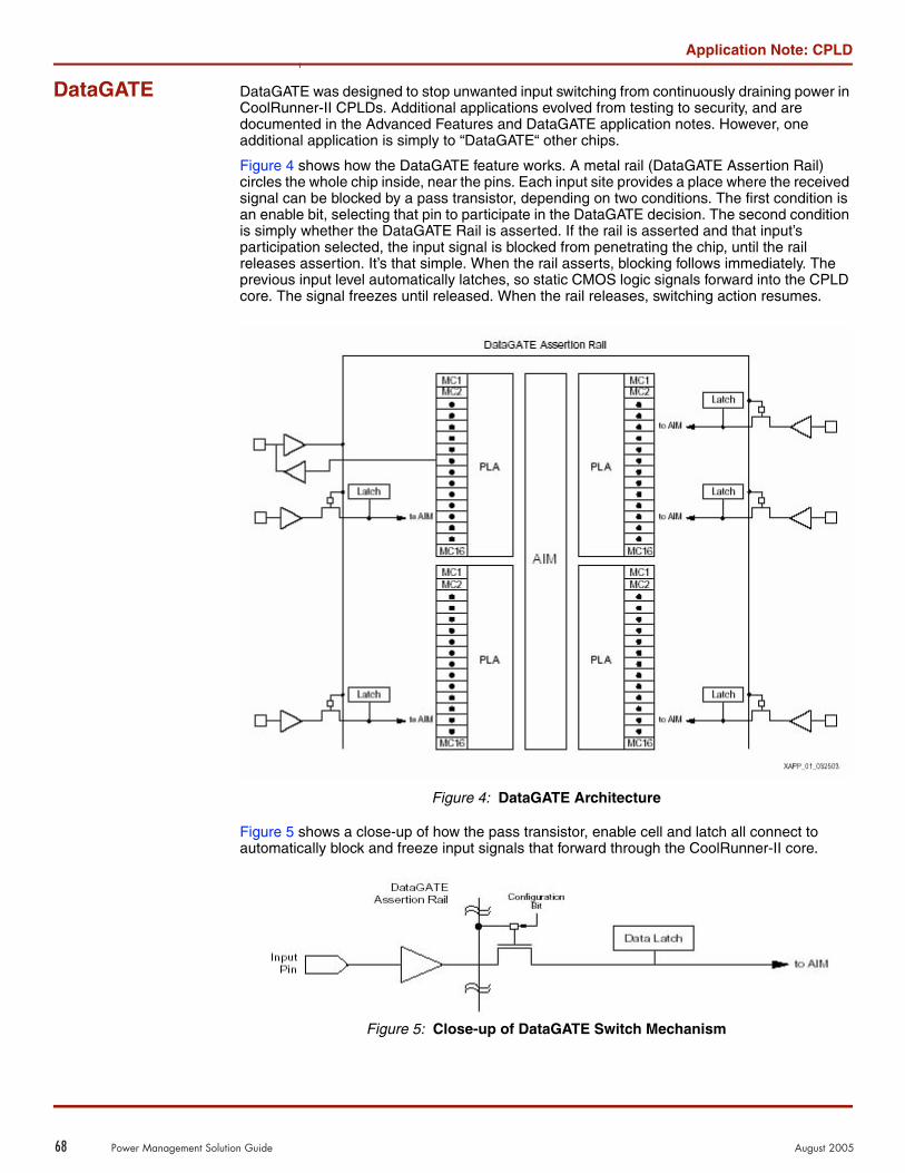
68 Power Management Solution Guide August 2005
DataGATER
DataGATE DataGATE was designed to stop unwanted input switching from continuously draining power inCoolRunner-II CPLDs. Additional applications evolved from testing to security, and aredocumented in the Advanced Features and DataGATE application notes. However, oneadditional application is simply to “DataGATE“ other chips.
Figure 4 shows how the DataGATE feature works. A metal rail (DataGATE Assertion Rail)circles the whole chip inside, near the pins. Each input site provides a place where the receivedsignal can be blocked by a pass transistor, depending on two conditions. The first condition is an enable bit, selecting that pin to participate in the DataGATE decision. The second conditionis simply whether the DataGATE Rail is asserted. If the rail is asserted and that input’s participation selected, the input signal is blocked from penetrating the chip, until the rail releases assertion. It’s that simple. When the rail asserts, blocking follows immediately. The previous input level automatically latches, so static CMOS logic signals forward into the CPLD core. The signal freezes until released. When the rail releases, switching action resumes.
Figure 5 shows a close-up of how the pass transistor, enable cell and latch all connect toautomatically block and freeze input signals that forward through the CoolRunner-II core.
Figure 4: DataGATE Architecture
Figure 5: Close-up of DataGATE Switch Mechanism
Application Note: CPLD

August 2005 Power Management Solution Guide 69
DataGATER
Figure 6 shows how signals passing through the CoolRunner-II DataGATE freeze signals toother chips. In this situation, we passed signals through the CoolRunner-II part, directly to theoutside, where they drive to other chips. These will be held at the logic level that was last on the input pad, when DataGATE asserts. Should a 3-state signal be forwarded through theCoolRunner-II output pins, it will naturally be pulled to a high or low value, by the weak keeper that is on them, thereby covering the case when a “frozen” output gets 3-stated by another condition. An interesting proposition of passing signals through the CoolRunner-II is that it might be done as a natural side product of simply translating voltage levels on signals as theyinterface through the CPLD. The DataGATE action, is really for free under those conditions,which occur frequently.
DataGATE is offered on CoolRunner-II CPLDS that have 128, 256, 384 and 512 macrocells. This extends into the hundreds of I/O pins that can be blocked as needed by the DataGATE facility. If multiple sets of pins need to be blocked, under different circumstances, then multiples of the smaller parts can be used to cover the number and condition needs of any given design.
At this point, we have not described what drives the DataGATE rail. It is very simple. One macrocell within a particular CoolRunner-II CPLD is designated as the “DataGATE” macrocell. It is identical to all other macrocells, which means any logic situation a designer sets up to drive that macrocell, asserts the DataGATE signal, if enabled in the design software. The DataGATEsignal releases whenever the logic driving that macrocell dictates. An event as simple as aswitching input can trigger the DataGATE macrocell, and an event as complex as a conditional state machine driving a timer can trigger the macrocell. Designers are free to dream upwhatever they want. It is possible to block any input chosen, including clocks, but extreme care must be used when designing that way! All, none or any subset of the input pins can beblocked. Being a reprogrammable CPLD, this facility can be used experimentally to determine the best set of signals to “freeze” and the best set of circumstances to assert and release the rail.
So, how do you know what to “freeze?” That will vary, from system to system. Here’s an example. When a microprocessor first bootstraps, it frequently sends values from its databus into a CPLD. These might be address values being loaded into comparators to select ranges ofmemory and I/O devices. Once those registers are initialized they need only compare againstthe address lines to operate. The databus connections are never needed again, but are still attached. DataGATE lets designers identify the time when the connection is no longer needed, and eliminate the extraneous switching that draws unneeded current. To learn more aboutother things you can do with DataGATE, check the references at the end.
Figure 6: DataGATE Blocking Switching Activity to Other Chips
Virtex-II
Spartan-3 ASSP
CoolRunner-II
CPLD
DataGATE
Rail
Outputs hold latch last
logic value when
DataGATE
Application Note: CPLD

70 Power Management Solution Guide August 2005
ConclusionR
Conclusion We have omitted some details. What is the power impact of unpowered I/O pins attached topowered up termination resistors? How much leakage per pin occurs if an unpowered pin is driven by a powered one? Many questions can only be answered by assessing the specific situations with the particular device’s data sheet in hand. We hope the methods described herewill have some value by simply increasing your choices on power reduction methods.
CoolRunner-II CPLDs are designed to be inherently low power devices. Additional features within them – including DataGATE, can help other chips also reduce their overall power, whenproperly applied.
References Portelligent Report #116.02-031023-1d
Estimation equation: http://www.xilinx.com/bvdocs/appnotes/xapp317.pdf
Low power design methods: http://www.xilinx.com/bvdocs/appnotes/xapp346.pdf
Decreasing power: http://www.xilinx.com/bvdocs/appnotes/xapp347.pdf
Accurate XPLA3 estimation: http://www.xilinx.com/bvdocs/appnotes/xapp360.pdf
Accurate CoolRunner-II Design estimation: http://www.xilinx.com/bvdocs/appnotes/xapp377.pdf
Powering CoolRunner-II: http://www.xilinx.com/bvdocs/appnotes/xapp389.pdf
DataGATE: http://www.xilinx.com/bvdocs/appnotes/xapp395.pdf
XPower http://www.xilinx.com/xlnx/xebiz/designResources/Power Estimator (Spartan) http://www.xilinx.com/cgi-bin/power_tool/power_Spartan3Power Estimator (Virtex-II) http://www.xilinx.com/cgi-bin/power_tool/power_Virtex2
Additional Information
CoolRunner-II Data Sheets, Application Notes, and White PapersDevice PackagesOnline StoreSpartan-3 Data Sheets, Application Notes, and White Papers
Application Note: CPLD

Would you like to write for Xcell
Publications?
It’s easier thanyou think.
Our Xcell Publishing Alliance can help you – from conceptresearch and development,
through planning and implementation, all the way
to publication and marketing.
Submit articles for our Web-based Xcell Online or any of ourprinted publications and we willassign an editor and a graphicsartist to work with you to make
your work look as good as possible. Submit your book
concepts and we will bring our broad industry resources to assist
you in planning, research, writing, editing, and marketing.
For more information on thisexciting and highly rewarding
program, please contact:
Forrest CouchManaging Editor, Xcell Publications
Get the Latest Virtex InfoDelivered to Your DesktopGet the Latest Virtex InfoDelivered to Your Desktop
Subscribe Now! www.xilinx.com/virtex4
Subscribe Now! www.xilinx.com/virtex4
R
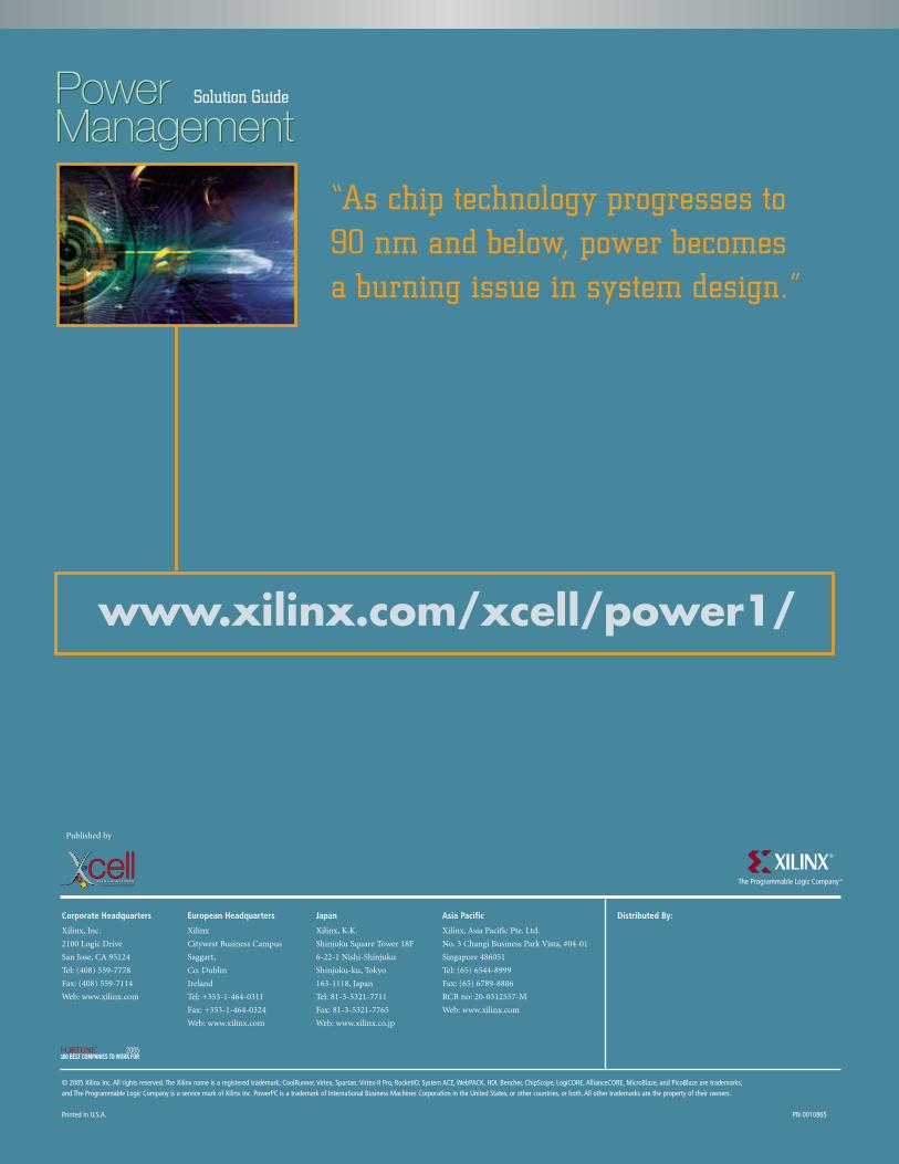
Corporate Headquarters
Xilinx, Inc.
2100 Logic Drive
San Jose, CA 95124
Tel: (408) 559-7778
Fax: (408) 559-7114
Web: www.xilinx.com
European Headquarters
Xilinx
Citywest Business Campus
Saggart,
Co. Dublin
Ireland
Tel: +353-1-464-0311
Fax: +353-1-464-0324
Web: www.xilinx.com
Japan
Xilinx, K.K.
Shinjuku Square Tower 18F
6-22-1 Nishi-Shinjuku
Shinjuku-ku, Tokyo
163-1118, Japan
Tel: 81-3-5321-7711
Fax: 81-3-5321-7765
Web: www.xilinx.co.jp
Asia Pacific
Xilinx, Asia Pacific Pte. Ltd.
No. 3 Changi Business Park Vista, #04-01
Singapore 486051
Tel: (65) 6544-8999
Fax: (65) 6789-8886
RCB no: 20-0312557-M
Web: www.xilinx.com
Distributed By:
© 2005 Xilinx Inc. All rights reserved. The Xilinx name is a registered trademark; CoolRunner, Virtex, Spartan, Virtex-II Pro, RocketIO, System ACE, WebPACK, HDL Bencher, ChipScope, LogiCORE, AllianceCORE, MicroBlaze, and PicoBlaze are trademarks;and The Programmable Logic Company is a service mark of Xilinx Inc. PowerPC is a trademark of International Business Machines Corporation in the United States, or other countries, or both. All other trademarks are the property of their owners.
Printed in U.S.A. PN 0010865
“As chip technology progresses to 90 nm and below, power becomes a burning issue in system design.”
Published by
PowerManagementPowerManagement
Solution Guide
www.xilinx.com/xcell/power1/