special-purpose operational amplifier circuits · pdf filespecial-purpose operational...
TRANSCRIPT

© 2012 Pearson Education. Upper Saddle River, NJ, 07458. All rights reserved.
Electronic Devices, 9th edition Thomas L. Floyd
Special-Purpose Operational Amplifier Circuits

© 2012 Pearson Education. Upper Saddle River, NJ, 07458. All rights reserved.
Electronic Devices, 9th edition Thomas L. Floyd
Instrumentation Amplifier
An instrumentation amplifier (IA) is a differential voltage-gain device that amplifies the difference between the voltages existing at its two input terminals.
The main purpose is to amplify small signals that may be riding on large common-mode voltages.
It is an integrated circuit that internally has three operational amplifiers and several resistors.
The key characteristics are high input impedance, high common-mode rejection, low output offset, and low output impedance.
Instrumentation amplifiers are commonly used in environments with high common mode noise such as in data acquisition systems where remote sensing of input variables is required

© 2012 Pearson Education. Upper Saddle River, NJ, 07458. All rights reserved.
Electronic Devices, 9th edition Thomas L. Floyd
Instrumentation Amplifier
Op-amps A1 and A2 are noninverting configurations that provide high input impedance and voltage gain.
Op-amp A3 is used as a unity-gain differential amplifier with high-precision resistors that are all equal in value (R3 = R4 = R5 = R6)
The gain-setting resistor, RG is connected externally.

© 2012 Pearson Education. Upper Saddle River, NJ, 07458. All rights reserved.
Electronic Devices, 9th edition Thomas L. Floyd
Instrumentation Amplifier
The overall closed-loop gain of the instrumentation amplifier is:
𝐴𝐴𝑐𝑐𝑐𝑐 = 1 +2𝑅𝑅𝑅𝑅𝐺𝐺
Where R1 = R2 = R The gain of the instrumentation amplifier can be set by the
value of the external resistor RG when R1 and R2 have a known fixed value.
The external gain-setting resistor RG can be calculated for a desired voltage gain by
𝑅𝑅𝐺𝐺 =2𝑅𝑅
𝐴𝐴𝑐𝑐𝑐𝑐 − 1

© 2012 Pearson Education. Upper Saddle River, NJ, 07458. All rights reserved.
Electronic Devices, 9th edition Thomas L. Floyd
Instrumentation Amplifier

© 2012 Pearson Education. Upper Saddle River, NJ, 07458. All rights reserved.
Electronic Devices, 9th edition Thomas L. Floyd
Instrumentation Amplifier

© 2012 Pearson Education. Upper Saddle River, NJ, 07458. All rights reserved.
Electronic Devices, 9th edition Thomas L. Floyd
Instrumentation Amplifier
Determine the value of the external gain-setting resistor RG for a certain IC instrumentation amplifier with R1 = R2 = 25 kΩ. The closed-loop voltage gain is to be 500.
Example
Solution
𝑅𝑅𝐺𝐺 =2𝑅𝑅
𝐴𝐴𝑐𝑐𝑐𝑐 − 1=
50 𝑘𝑘Ω500 − 1
≅ 100Ω

© 2012 Pearson Education. Upper Saddle River, NJ, 07458. All rights reserved.
Electronic Devices, 9th edition Thomas L. Floyd
Instrumentation Amplifier
The instrumentation amplifier is normally used to measure small differential signal voltages that are superimposed on a common-mode voltage often much larger than the signal voltage. Applications include situations where a quantity is sensed by a remote device and the resulting small electrical signal is sent over a long line subject to electrical noise that produces common-mode voltages in the line.

© 2012 Pearson Education. Upper Saddle River, NJ, 07458. All rights reserved.
Electronic Devices, 9th edition Thomas L. Floyd
AD622 Instrumentation Amplifier
An external resistor must be used to achieve a voltage gain greater than unity.
RG is connected between pins 1 and 8.
𝑅𝑅𝐺𝐺 =50.5 𝑘𝑘Ω𝐴𝐴𝑐𝑐𝑐𝑐 − 1

© 2012 Pearson Education. Upper Saddle River, NJ, 07458. All rights reserved.
Electronic Devices, 9th edition Thomas L. Floyd
AD622 Instrumentation Amplifier
What value of RG will set the gain to 35?
= 1.5 kΩ
G50.5 k 50.5 k
1 35 1v
RA
Ω Ω= =
− −

© 2012 Pearson Education. Upper Saddle River, NJ, 07458. All rights reserved.
Electronic Devices, 9th edition Thomas L. Floyd
Instrumentation Amplifiers
The bandwidth of any IA (or op-amp for that matter) is lower for higher gain. The graph shows the BW for various gains for the AD622.
What is the BW for a gain of 35?
0
Volta
ge g
ain
100Frequency (Hz)
1
1k 10k 100k 1M 10M
10
100
1000
Reading the graph, the BW is approximately 200 kHz.

© 2012 Pearson Education. Upper Saddle River, NJ, 07458. All rights reserved.
Electronic Devices, 9th edition Thomas L. Floyd
Noise Effects in IA Applications
Various types of transducers are used to sense temperature, strain, pressure, and other parameters in many types of applications.
Instrument amplifiers are generally used to process the small voltages produces by a transducer and in noisy industrial environment.
Noise in the form of common mode signals picked up from external sources can be minimized, but not totally eliminated, by using coaxial cable in which the different signal wires are surrounded by a metal mesh sheathing called a shield.
In an electrically noisy environment any common-mode signal that are induced on the signal lines are rejected because both inputs to the amplifier have the same common-mode signal.

© 2012 Pearson Education. Upper Saddle River, NJ, 07458. All rights reserved.
Electronic Devices, 9th edition Thomas L. Floyd
Noise Effects in IA Applications
However, when a shielded cable used, there are stray capacitance distributed along its length between each signal line and the shield.
The difference in these stray capacitance, particularly at higher frequencies result in a phase shift between the two common-mode signals, as illustrated.

© 2012 Pearson Education. Upper Saddle River, NJ, 07458. All rights reserved.
Electronic Devices, 9th edition Thomas L. Floyd
SHIELD GUARD
Guarding is a technique to reduce the effect of noise on the common-mode operation of an instrument amplifier by connecting the common-mode voltage to the shield of a coaxial cable.
The common-mode signal is fed back to the shield by a voltage-follower stage
The purpose is to eliminated voltage differences between the signal lines and the shield, virtually eliminating leakage current and cancelling the effects of the distributed capacitance so that the common-mode voltages are the same in both lines.
Noise Effects in IA Applications

© 2012 Pearson Education. Upper Saddle River, NJ, 07458. All rights reserved.
Electronic Devices, 9th edition Thomas L. Floyd
The voltage-follower is a low-impendence source that drives the common-mode signal onto the shield to eliminate the voltage difference between the signal lines and the shield.
When the voltage between each signal line and the shield is zero, the leakage current are also zero and the capacitive reactance become infinity large. An infinitely large Xc implies a zero capacitance
Noise Effects in IA Applications

© 2012 Pearson Education. Upper Saddle River, NJ, 07458. All rights reserved.
Electronic Devices, 9th edition Thomas L. Floyd
Instrumentation Amplifiers
The AD522 is a low-noise IA that has a Data guard output, which is connected to the shield as shown. The AD522 has a programmed gain from 1 to 1000 depending on RG. The frequency response rolls off at −20 dB/decade.
10 100 1k 10k 100k 1Mf (Hz)
60
40
20
0
(dB)Gain
G = 1000
G = 100
G = 10
G = 1
Frequency response of AD522

© 2012 Pearson Education. Upper Saddle River, NJ, 07458. All rights reserved.
Electronic Devices, 9th edition Thomas L. Floyd
Isolation Amplifiers
An isolation amplifier is designed to provide an electrical barrier between the input and output.
It consists of two electrically isolated stages: Input stage and Output stage separated by an isolation barrier so that a signal must be processed in order to be coupled across the isolation barrier.
It is used for the protection of human life or sensitive equipment in those applications where hazardous power-line leakage or high-voltage transients are possible.
Some isolation amplifiers use optical coupling or transformer coupling to provide isolation between the stages.
Modern isolation amplifiers use capacitive coupling for isolation.
In each stages, supply voltages and grounds are separated so that there are no common electrical paths between them.

© 2012 Pearson Education. Upper Saddle River, NJ, 07458. All rights reserved.
Electronic Devices, 9th edition Thomas L. Floyd
Isolation Amplifiers
A simplified block diagram for a typical capacitor coupled isolation amplifier
Notice that there are two different ground symbols are used to reinforce the concept of stage separation.

© 2012 Pearson Education. Upper Saddle River, NJ, 07458. All rights reserved.
Electronic Devices, 9th edition Thomas L. Floyd
Isolation Amplifiers
The input stage consists of an amplifier, an oscillator and a modulator.
The modulator uses a high-frequency square-wave oscillator to modify the original signal.
A small-value capacitor in the isolation barrier is used to couple the lower frequency modulated signal or dc voltage from the input to the output.
The output stage consists of a demodulator that extracts the original input signal from the modulated signal so that the original signal from the input stage is back to its original form.
When separate dc supply voltages and an input signal are applied, an amplified output signal is the result.

© 2012 Pearson Education. Upper Saddle River, NJ, 07458. All rights reserved.
Electronic Devices, 9th edition Thomas L. Floyd
Isolation Amplifiers
An isolation amplifier that uses pulse width modulation is shown

© 2012 Pearson Education. Upper Saddle River, NJ, 07458. All rights reserved.
Electronic Devices, 9th edition Thomas L. Floyd
The ISO124 is a capacitively-coupled isolation amplifier that uses pulse width modulation to transmit data across the barrier.
The ISO124 has fixed unity gain and is rated to 1500 Vrms of isolation. The frequency response is specified to 50 kHz, but high-frequency ripple due to the PW modulation may be observed on the output at higher frequencies. The supply voltages should be coupled with external capacitors to reduce noise
(7)Outputsignal
Input signal
IS0124
(1)(2)
–15 V
(15)
+15 V
(16)(9)
–15 V+15 V
1 Fµ
1 Fµ1 Fµ
1 Fµ
(10)(8)
Input Stage
Output Stage
Barrier
Output waveform
Isolation Amplifiers

© 2012 Pearson Education. Upper Saddle River, NJ, 07458. All rights reserved.
Electronic Devices, 9th edition Thomas L. Floyd
Transformer-Coupled Isolation Amplifier
Gain of the input stage:
𝐴𝐴𝑣𝑣1 =𝑅𝑅𝑓𝑓1𝑅𝑅𝑖𝑖1
+ 1
Gain of the output stage:
𝐴𝐴𝑣𝑣2 =𝑅𝑅𝑓𝑓2𝑅𝑅𝑖𝑖2
+ 1
The total amplifier gain is 𝐴𝐴𝑣𝑣(𝑡𝑡𝑡𝑡𝑡𝑡) = 𝐴𝐴𝑣𝑣1𝐴𝐴𝑣𝑣2
3656KG is an example of an isolation amplifier that uses transformer coupling to isolate the two stages. The 3656KG can have gain for both the input and output stages. The 3656KG is suited for patient monitoring applications, such as an ECG amplifier.
Rf 2
Rf1
Ri1
(10)
(7)
(6) (15)
(14)
(20)(19)
(16)(12)
Vin
Vout
+VDC
Ri2
(3)
Rs
Input Output

© 2012 Pearson Education. Upper Saddle River, NJ, 07458. All rights reserved.
Electronic Devices, 9th edition Thomas L. Floyd
Fetal Heartbeat Monitoring
A simplified diagram of an isolation amplifier in a cardiac-monitoring application is shown. In this situation, heart signals, which are very small, are combined with much larger common-mode signals caused by muscle noise, electrochemical noise, residual electrode voltage, and 60 Hz power-line pickup from the skin.

© 2012 Pearson Education. Upper Saddle River, NJ, 07458. All rights reserved.
Electronic Devices, 9th edition Thomas L. Floyd
Example: Determine the total voltage gain of the 3656KG isolation amplifier in Figure 14–15.

© 2012 Pearson Education. Upper Saddle River, NJ, 07458. All rights reserved.
Electronic Devices, 9th edition Thomas L. Floyd
The Operational Transconductance Amplifier
The operational transconductance amplifier (OTA) is a voltage-to-current amplifier in which the output current equals the gain times the input voltage. Like the conventional op-amp, the OTA has two differential input terminals, a high input impedance, and a high CMRR.
The OTA has a bias-current input terminal, a high output impedance, and no fixed open-loop voltage gain.
The voltage-to-current gain of an OTA is the transconductance,
𝑔𝑔𝑚𝑚 =𝐼𝐼𝑡𝑡𝑜𝑜𝑡𝑡𝑉𝑉𝑖𝑖𝑖𝑖

© 2012 Pearson Education. Upper Saddle River, NJ, 07458. All rights reserved.
Electronic Devices, 9th edition Thomas L. Floyd
The Operational Transconductance Amplifier
In an OTA, the transconductance is dependent on a constant (K) times the bias current (IBIAS). The value of the constant K is dependent on the internal circuit design: gm = K IBIAS
A typical relationship of the transconductance and the bias current is illustrated. The transconductance increases linearly with the bias current. The proportionality constant, K, is the slope of the line. In this case, K is approximately 16 μS/μA
The output current is controlled by the input voltage and the bias current: Iout = gmVin = K IBIAS Vin

© 2012 Pearson Education. Upper Saddle River, NJ, 07458. All rights reserved.
Electronic Devices, 9th edition Thomas L. Floyd
Basic OTA Circuits
An OTA used as an inverting amplifier with a fixed voltage gain is shown. The voltage gain is set by the transconductance and the load resistance as follows:
The transconductance of the amplifier shown is determined by the amount of bias current, which is set by the dc supply voltages and the bias resistor RBIAS .

© 2012 Pearson Education. Upper Saddle River, NJ, 07458. All rights reserved.
Electronic Devices, 9th edition Thomas L. Floyd
The voltage gain can be controlled by the amount of bias current. This can be done manually by using a variable resistor in series with RBIAS .The voltage gain can also be controlled with an externally applied variable voltage.
Basic OTA Circuits

© 2012 Pearson Education. Upper Saddle River, NJ, 07458. All rights reserved.
Electronic Devices, 9th edition Thomas L. Floyd
A Specific OTA
The LM13700 is a dual device package containing two OTAs and buffer circuits. The maximum dc supply voltages are ± 18 V. The bias current is determined by the following formula:
The positive bias voltage, +VBIAS , may be obtained from the positive supply voltage, +V

© 2012 Pearson Education. Upper Saddle River, NJ, 07458. All rights reserved.
Electronic Devices, 9th edition Thomas L. Floyd
The Operational Transconductance Amplifier
Example: The OTA in Figure is connected as an inverting fixed-gain amplifier where +VBIAS = +V. Determine the approximate voltage gain for K = 16 μS/μA.

© 2012 Pearson Education. Upper Saddle River, NJ, 07458. All rights reserved.
Electronic Devices, 9th edition Thomas L. Floyd
OTA Application: Amplitude Modulator
An OTA connected as an amplitude modulator is shown. The voltage gain is varied by applying a modulation voltage to the bias input.
When a constant-amplitude input signal is applied, the amplitude of the output signal will vary according to the modulation voltage on the bias input.
The gain is dependent on bias current, and bias current is related to the modulation voltage by the following relationship:

© 2012 Pearson Education. Upper Saddle River, NJ, 07458. All rights reserved.
Electronic Devices, 9th edition Thomas L. Floyd
OTA Application: Amplitude Modulator

© 2012 Pearson Education. Upper Saddle River, NJ, 07458. All rights reserved.
Electronic Devices, 9th edition Thomas L. Floyd
OTA Application: Amplitude Modulator

© 2012 Pearson Education. Upper Saddle River, NJ, 07458. All rights reserved.
Electronic Devices, 9th edition Thomas L. Floyd
OTA Application: Amplitude Modulator

© 2012 Pearson Education. Upper Saddle River, NJ, 07458. All rights reserved.
Electronic Devices, 9th edition Thomas L. Floyd
OTA Application: Amplitude Modulator
© 2012 Pearson Education. Upper Saddle River, NJ, 07458. All rights reserved.
Electronic Devices, 9th edition Thomas L. Floyd
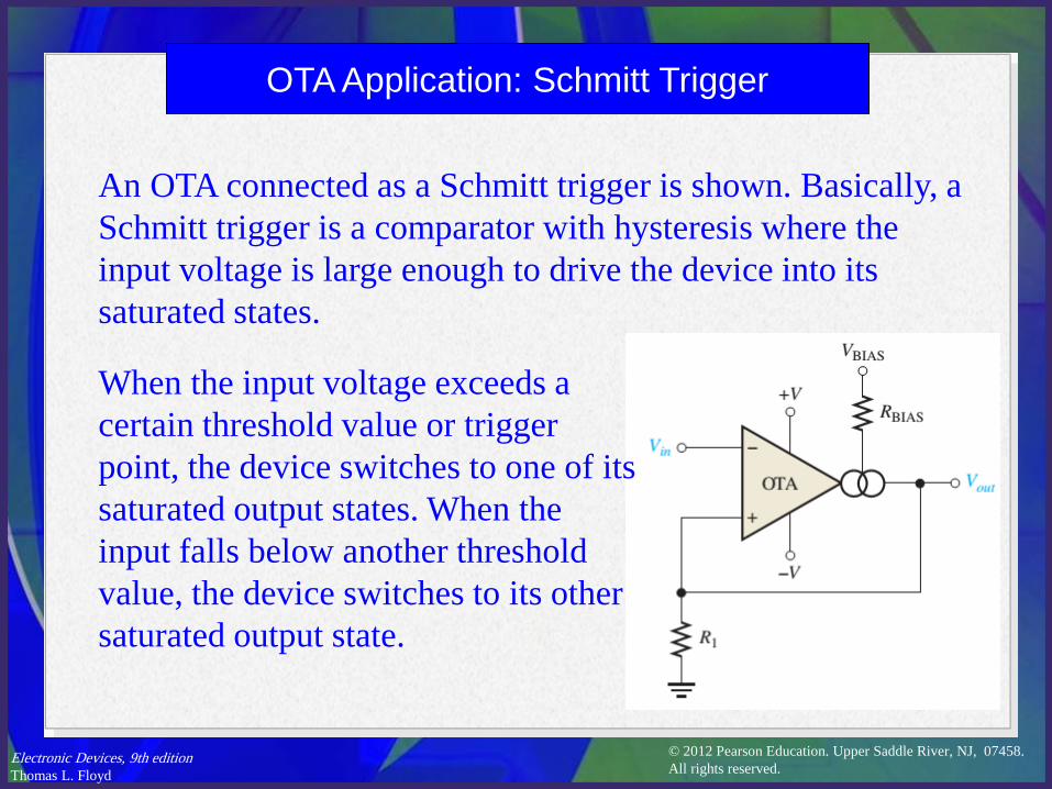
OTA Application: Schmitt Trigger
An OTA connected as a Schmitt trigger is shown. Basically, a Schmitt trigger is a comparator with hysteresis where the input voltage is large enough to drive the device into its saturated states.
When the input voltage exceeds a certain threshold value or trigger point, the device switches to one of its saturated output states. When the input falls below another threshold value, the device switches to its other saturated output state.

© 2012 Pearson Education. Upper Saddle River, NJ, 07458. All rights reserved.
Electronic Devices, 9th edition Thomas L. Floyd
OTA Application: Schmitt Trigger
In the case of the OTA Schmitt trigger, the threshold levels are set by the current through resistor R1 .The maximum output current in an OTA equals the bias current.
Therefore, in the saturated output states, Iout = IBIAS .
The maximum positive output voltage is Iout R1 and this voltage is the positive threshold value or upper trigger point. When the input voltage exceeds this value, the output switches to its maximum negative voltage, which is - Iout R1.
Since Iout = IBIAS, the trigger points can be controlled by the bias current.

© 2012 Pearson Education. Upper Saddle River, NJ, 07458. All rights reserved.
Electronic Devices, 9th edition Thomas L. Floyd
OTA Application: Schmitt Trigger

© 2012 Pearson Education. Upper Saddle River, NJ, 07458. All rights reserved.
Electronic Devices, 9th edition Thomas L. Floyd
The Logarithmic Amplifier
Log and antilog amplifiers are used in applications that require compression of analog input data, linearization of transducers that have exponential outputs, and analog multiplication and division.
They are often used in high-frequency communication systems, including fiber optics, for processing wide dynamic range signals.
The semiconductor pn junction in the form of either a diode or the base-emitter junction of a BJT provides a logarithmic characteristic.
The diode characteristic curve is shown , where VF is the forward diode voltage and IF is the forward diode current.

© 2012 Pearson Education. Upper Saddle River, NJ, 07458. All rights reserved.
Electronic Devices, 9th edition Thomas L. Floyd
The Logarithmic Amplifier
The current voltage relation is:
𝐼𝐼𝐹𝐹 = 𝐼𝐼𝑅𝑅𝑒𝑒𝑞𝑞𝑉𝑉𝐹𝐹/𝑘𝑘𝑘𝑘
Solving for VF we get:
𝑉𝑉𝐹𝐹 =𝑘𝑘𝑘𝑘𝑞𝑞
ln𝐼𝐼𝐹𝐹𝐼𝐼𝑅𝑅
The output is limited to a maximum value of approximately 0.7 V because the diode’s logarithmic characteristic is restricted to voltages below 0.7 V.

© 2012 Pearson Education. Upper Saddle River, NJ, 07458. All rights reserved.
Electronic Devices, 9th edition Thomas L. Floyd
The Logarithmic Amplifier
When a diode is placed in the feedback loop of an op-amp circuit, the output voltage is proportional to the log of the input voltage. From the circuit we have:
𝑉𝑉𝑡𝑡𝑜𝑜𝑡𝑡 = −𝑉𝑉𝐹𝐹
𝐼𝐼𝐹𝐹 = 𝐼𝐼𝑖𝑖𝑖𝑖 =𝑉𝑉𝑖𝑖𝑖𝑖𝑅𝑅1
Substituting into the formula for VF we get:
𝑉𝑉𝑡𝑡𝑜𝑜𝑡𝑡 = −𝑘𝑘𝑘𝑘𝑞𝑞
ln𝑉𝑉𝑖𝑖𝑖𝑖𝐼𝐼𝑅𝑅𝑅𝑅1
= −(0.025𝑉𝑉) ln𝑉𝑉𝑖𝑖𝑖𝑖𝐼𝐼𝑅𝑅𝑅𝑅1
The gain decreases with increasing input voltage; therefore the amplifier is said to compress signals.
R1
–
+
Op-amp Vout
+ –VF
IFIin
Vin
0 V

© 2012 Pearson Education. Upper Saddle River, NJ, 07458. All rights reserved.
Electronic Devices, 9th edition Thomas L. Floyd
The Logarithmic Amplifier
For the circuit shown, the equation for Vout is
( )R 1
0.025 V ln inout
VVI R
≅ − (IR is a constant for a given diode.)
R1
–
+
Op-amp Vout
+ –VF
IFIin
Vin
0 V
What is Vout? (Assume IR = 50 nA.)
( ) ( )( )11 V0.025 V ln
50 nA 1.0 koutV ≅ −Ω
= −307 mV
R1
–
+
Op-amp Vout
+ –VF
Vin
+11 V1.0 kΩ

© 2012 Pearson Education. Upper Saddle River, NJ, 07458. All rights reserved.
Electronic Devices, 9th edition Thomas L. Floyd
The Logarithmic Amplifier
When a BJT is used in the feedback path, the output is referred to the ground of the base connection rather than the virtual ground. This eliminates offset and bias current errors. For the BJT, IEBO (emitter-to-base leakage current) replaces IR in the equation for Vout:
( )EBO 1
0.025 V ln inout
VVI R
= −
R1
–
+
Op-amp Vout
+
–VBE
ICIin
Vin
0 V
Log amplifiers are available in IC form with even better performance than the basic log amps shown here. For example, the MAX4206 operates over 5 decades and can measure current from 10 nA to 1 mA.

© 2012 Pearson Education. Upper Saddle River, NJ, 07458. All rights reserved.
Electronic Devices, 9th edition Thomas L. Floyd
The Antilog Amplifier
An antilog amplifier is formed by connecting a transistor (or diode) as the input element as shown. We have:
𝑉𝑉𝑡𝑡𝑜𝑜𝑡𝑡 = −𝑅𝑅𝑓𝑓𝐼𝐼𝐶𝐶 , 𝐼𝐼𝐶𝐶 = 𝐼𝐼𝐸𝐸𝐸𝐸0𝑒𝑒𝑞𝑞𝑉𝑉𝐵𝐵𝐵𝐵/𝑘𝑘𝑘𝑘 𝑉𝑉𝑡𝑡𝑜𝑜𝑡𝑡 = −𝑅𝑅𝑓𝑓𝐼𝐼𝐸𝐸𝐸𝐸0𝑒𝑒𝑞𝑞𝑉𝑉𝐵𝐵𝐵𝐵/𝑘𝑘𝑘𝑘
The equation for Vout for the basic BJT antilog amp is:
EBOantilog25 mV
inout f
VV R I= −
Rf
–
+
Op-amp Vout
–
+VBE
IC
Vin
0 V
+ –IC antilog amps are also available. For example, the Datel LA-8048 is a log amp and the Datel LA-8049 is its counterpart antilog amp. These ICs are specified for a six decade range.

© 2012 Pearson Education. Upper Saddle River, NJ, 07458. All rights reserved.
Electronic Devices, 9th edition Thomas L. Floyd
The Antilog Amplifier
EXAMPLE: For the antilog amplifier in Figure, find the output voltage. Assume IEBO = 40 nA.
EBOantilog25 mV
inout f
VV R I= − = -3 V.

© 2012 Pearson Education. Upper Saddle River, NJ, 07458. All rights reserved.
Electronic Devices, 9th edition Thomas L. Floyd
Constant-Current Source
A constant-current source delivers a load current that remains constant when the load resistance changes.
From the figure we get:
𝐼𝐼𝐿𝐿 = 𝐼𝐼𝑖𝑖 =𝑉𝑉𝐼𝐼𝐼𝐼𝑅𝑅𝑖𝑖
If RL changes, IL remains constant as long as VIN and Ri are held constant
RLRi
Ii
–
+
–
+VIN
0 A0 V
IL = Ii
Constant-current source

© 2012 Pearson Education. Upper Saddle River, NJ, 07458. All rights reserved.
Electronic Devices, 9th edition Thomas L. Floyd
Current-to-Voltage Converter
A current-to-voltage converter converts a variable input current to a proportional output voltage. A basic circuit that accomplishes this is shown. From the figure we get:
𝑉𝑉𝑡𝑡𝑜𝑜𝑡𝑡 = 𝐼𝐼𝑖𝑖𝑅𝑅𝑓𝑓
Current-to-voltage converter
Ii–
+
0 VVout
Ii
Rf

© 2012 Pearson Education. Upper Saddle River, NJ, 07458. All rights reserved.
Electronic Devices, 9th edition Thomas L. Floyd
Voltage-to-Current Converter
A basic voltage-to-current converter is shown. This circuit is used in applications where it is necessary to have an output (load) current that is controlled by an input voltage. From the figure we get:
𝐼𝐼𝐿𝐿 =𝑉𝑉𝑖𝑖𝑖𝑖𝑅𝑅1
Voltage-to-current converter
Vin +
–
I = 0IL RL
R1I1

© 2012 Pearson Education. Upper Saddle River, NJ, 07458. All rights reserved.
Electronic Devices, 9th edition Thomas L. Floyd
Peak Detector
This circuit is used to detect the peak of the input voltage and store that peak voltage on a capacitor. When a positive voltage is applied to the noninverting input of the op-amp, the high-level output voltage of the op-amp forward-biases the diode and charges the capacitor. The capacitor continues to charge until its voltage reaches a value equal to the input voltage and thus both op-amp inputs are at the same voltage.
Peak detector
Vin +
–R1
Vout
Ri
C
At this point, the op-amp comparator switches, and its output goes to the low level. The diode is now reverse biased, and the capacitor stops charging. If a greater input peak occurs, the capacitor charges to the new peak

© 2012 Pearson Education. Upper Saddle River, NJ, 07458. All rights reserved.
Electronic Devices, 9th edition Thomas L. Floyd
Selected Key Terms
Instrumentation amplifier
Isolation amplifier
Operational transconductance
amplifier
Transconductance
An amplifier used for amplifying small signals riding on large common-mode voltages.
An amplifier with electrically isolated internal stages.
A voltage-to-current amplifier.
In an electronic device, the ratio of the output current to the input voltage.

© 2012 Pearson Education. Upper Saddle River, NJ, 07458. All rights reserved.
Electronic Devices, 9th edition Thomas L. Floyd
Quiz
1. A typical instrumentation amplifier has
a. high CMRR
b. unity gain
c. low input impedance
d. all of the above

© 2012 Pearson Education. Upper Saddle River, NJ, 07458. All rights reserved.
Electronic Devices, 9th edition Thomas L. Floyd
Quiz
2. When an instrumentation amplifier uses guarding, the shield is driven by a
a. low-impedance differential source
b. low-impedance common-mode source
c. high-impedance differential source
d. high-impedance common-mode source
© 2012 Pearson Education. Upper Saddle River, NJ, 07458. All rights reserved.
Electronic Devices, 9th edition Thomas L. Floyd
Quiz
3. You can achieve a higher bandwidth for an instrumentation amplifier if you
a. use guarding
b. use a larger gain setting resistor
c. capacitively couple the input signal
d. none of the above

© 2012 Pearson Education. Upper Saddle River, NJ, 07458. All rights reserved.
Electronic Devices, 9th edition Thomas L. Floyd
Quiz
4. An application where an isolation amplifier is particularly useful is when
a. the input signal has very large dynamic range
b. control of the frequency response is necessary
c. voltages could present a hazard
d. all of the above

© 2012 Pearson Education. Upper Saddle River, NJ, 07458. All rights reserved.
Electronic Devices, 9th edition Thomas L. Floyd
Quiz
5. For an OTA, the gain is determined by
a. a ratio of two resistors
b. bias current
c. a single gain setting resistor
d. the amplitude of the input signal

© 2012 Pearson Education. Upper Saddle River, NJ, 07458. All rights reserved.
Electronic Devices, 9th edition Thomas L. Floyd
Quiz
6. Transconductance is the ratio of
a. output current to input voltage
b. input current to output voltage
c. output resistance to input resistance
d. output voltage to input current
© 2012 Pearson Education. Upper Saddle River, NJ, 07458. All rights reserved.
Electronic Devices, 9th edition Thomas L. Floyd
Quiz
7. A circuit that is useful for signal compression is a
a. instrumentation amplifier
b. OTA
c. logarithmic amplifier
d. antilog amplifier

© 2012 Pearson Education. Upper Saddle River, NJ, 07458. All rights reserved.
Electronic Devices, 9th edition Thomas L. Floyd
Quiz
8. The circuit shown here is a
a. peak detector
b. current-to-voltage converter
c. voltage-to-current converter
d. isolation amplifier
Vin +
–
I = 0IL RL
R1I1

© 2012 Pearson Education. Upper Saddle River, NJ, 07458. All rights reserved.
Electronic Devices, 9th edition Thomas L. Floyd
Quiz
9. The circuit shown here is a
a. current-to-voltage converter
b. constant current source
c. logarithmic amplifier
d. antilog amp
Rf
–
+
Op-amp Vout
–
+VBE
IC
Vin
0 V
+ –

© 2012 Pearson Education. Upper Saddle River, NJ, 07458. All rights reserved.
Electronic Devices, 9th edition Thomas L. Floyd
Quiz
10. The circuit shown here is a
a. current-to-voltage converter
b. voltage-to-current converter
c. constant current source
d. peak detector
Vin +
–R1
Vout
Ri
C

© 2012 Pearson Education. Upper Saddle River, NJ, 07458. All rights reserved.
Electronic Devices, 9th edition Thomas L. Floyd
Quiz
Answers:
1. a
2. b
3. d
4. c
5. b
6. a
7. c
8. c
9. d
10. d