specifications - data-modul.com · appendix ackey 08/25/2015 01 005 show backlight life time 8...
TRANSCRIPT

TECH. CORP.
SPECIFICATIONS
CUSTOMER :
SAMPLE CODE : SH320240T-023-I03Q
MASS PRODUCTION CODE : PH320240T-023-I03Q
SAMPLE VERSION : 01
SPECIFICATIONS EDITION : 006
DRAWING NO. (Ver.) : LMD-PH320240T-023-I03Q (Ver.003)
PACKAGING NO. (Ver.) : PKG-PH320240T-023-I03Q (Ver.001)
Customer Approved
Date:
Approved Checked Designer
黃秋源黃秋源黃秋源黃秋源
Oliver Huang
石建莊石建莊石建莊石建莊
Stone Shin
黃俊清黃俊清黃俊清黃俊清
Ackey Huang
Preliminary specification for design input
Specification for sample approval
POWERTIP TECH. CORP.
Headquarters: No.8, 6th Road, Taichung Industrial Park,
Taichung, Taiwan 台中市 407工業區六路 8號
TEL: 886-4-2355-8168
FAX: 886-4-2355-8166
E-mail: [email protected]
Http://www.powertip.com.tw
NO.PT-A-005-8

PH320240T-023-I03Q Page2 SAMPLE Ver.01 SPEC Edi.006
History of Version
Date Ver. Edi. Description Page Design by
12/07/2012 01 001 New Drawing. - Ackey
12/17/2012 01 002
Modify Interface Pin Description
(LEDA->A , LEDK->K , Y2->Y+ , X2->X+ ,
Y1->Y- , X1->X-)
- Ackey
01/17/2013 01 003 New Sample. - Ackey
04/03/2014 01 004 Modify CR & Viewing Angle.
Add CN & Initcode.
6,17
Appendix Ackey
08/25/2015 01 005 Show Backlight Life Time 8 張斌
02/02/2016 01 006 Modify Initial Code Comment. 14 Ackey
Total: 32 Page

PH320240T-023-I03Q Page3 SAMPLE Ver.01 SPEC Edi.006
Contents
1. SPECIFICATIONS 1.1 Features 1.2 Mechanical Specifications 1.3 Absolute Maximum Ratings 1.4 DC Electrical Characteristics 1.5 Optical Characteristics 1.6 Backlight Characteristics 1.7 Touch Panel Characteristics
2. MODULE STRUCTURE 2.1 Counter Drawing 2.2 Interface Pin Description
2.2.1 Refer Initial code 2.3 Timing Characteristics
3. QUALITY ASSURANCE SYSTEM 3.1 Quality Assurance Flow Chart 3.2 Inspection Specification
4. RELIABILITY TEST 4.1 Reliability Test Condition
5. PRECAUTION RELATING PRODUCT HANDLING 5.1 Safety 5.2 Handling 5.3 Storage 5.4 Terms of Warranty
Appendix::::LCM Drawing
LCM Packaging Specifications
Note : For detailed information please refer to IC data sheet : Primacy(TFT LCD): Himax: HX8238-D
PH320240T-023-I03Q Page4 SAMPLE Ver.01 SPEC Edi.006
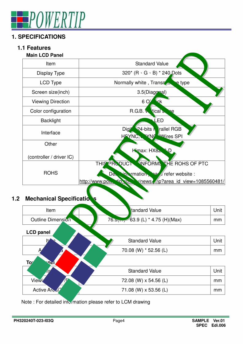
1. SPECIFICATIONS
1.1 Features
Main LCD Panel
Item Standard Value
Display Type 320* (R、G、B) * 240 Dots
LCD Type Normally white , Transmissive type
Screen size(inch) 3.5(Diagonal)
Viewing Direction 6 O’clock
Color configuration R.G.B. vertical stripe
Backlight White LED
Interface Digital 24-bits Parallel RGB
HSYNC,VSYNC.3Wires SPI
Other
(controller / driver IC)
Himax: HX8238-D
ROHS
THIS PRODUCT CONFORMS THE ROHS OF PTC
Detail information please refer website :
http://www.powertip.com.tw/news.php?area_id_view=1085560481/
1.2 Mechanical Specifications
Item Standard Value Unit
Outline Dimension 76.9(W) * 63.9 (L) * 4.75 (H)(Max) mm
LCD panel
Item Standard Value Unit
Active Area 70.08 (W) * 52.56 (L) mm
Touch panel
Item Standard Value Unit
Viewing Area(T/P) 72.08 (W) x 54.56 (L) mm
Active Area(T/P) 71.08 (W) x 53.56 (L) mm
Note : For detailed information please refer to LCM drawing
PH320240T-023-I03Q Page5 SAMPLE Ver.01 SPEC Edi.006
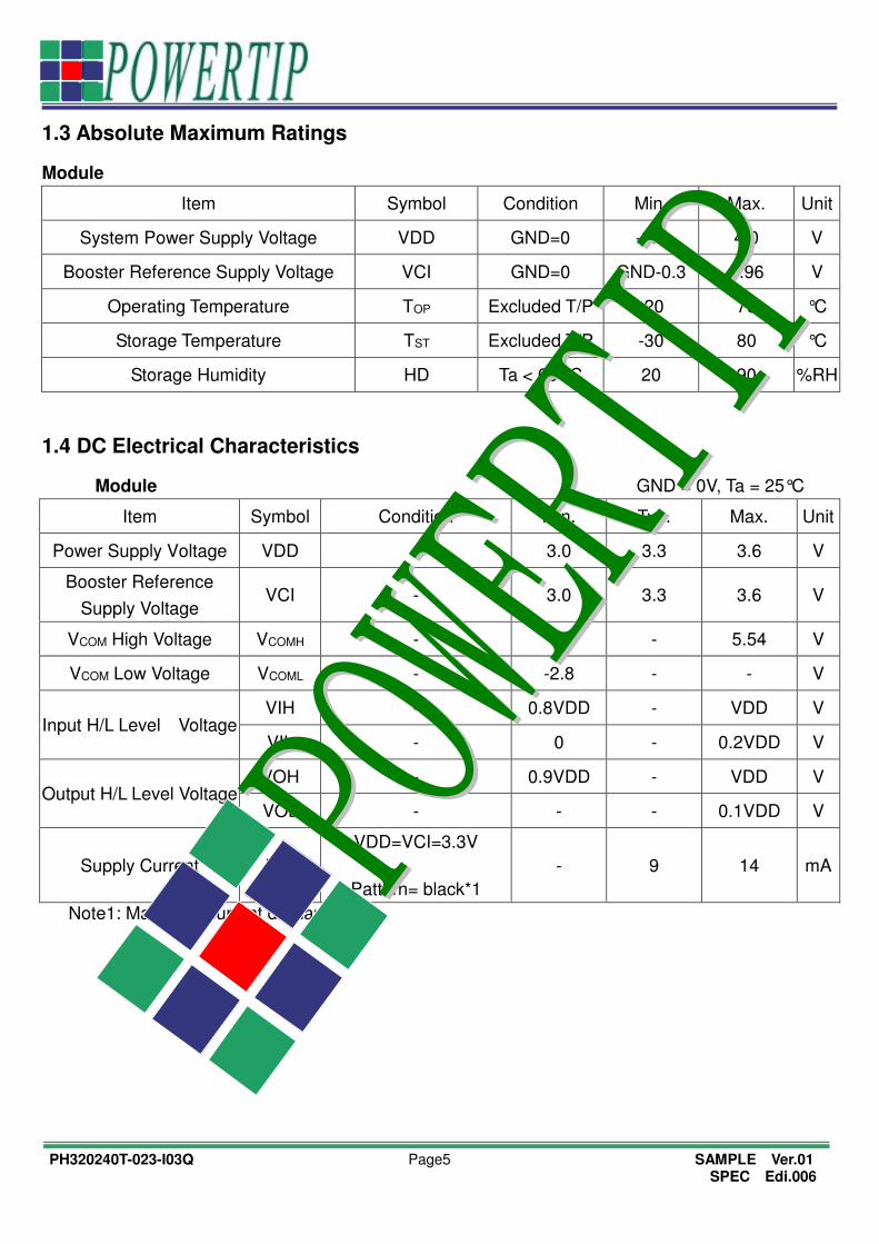
1.3 Absolute Maximum Ratings
Module
Item Symbol Condition Min. Max. Unit
System Power Supply Voltage VDD GND=0 -0.3 4.0 V
Booster Reference Supply Voltage VCI GND=0 GND-0.3 3.96 V
Operating Temperature TOP Excluded T/P -20 70 °C
Storage Temperature TST Excluded T/P -30 80 °C
Storage Humidity HD Ta < 60 °C 20 90 %RH
1.4 DC Electrical Characteristics
Module GND = 0V, Ta = 25°C
Item Symbol Condition Min. Typ. Max. Unit
Power Supply Voltage VDD - 3.0 3.3 3.6 V
Booster Reference
Supply Voltage VCI - 3.0 3.3 3.6 V
VCOM High Voltage VCOMH - - - 5.54 V
VCOM Low Voltage VCOML - -2.8 - - V
Input H/L Level Voltage VIH - 0.8VDD - VDD V
VIL - 0 - 0.2VDD V
Output H/L Level Voltage VOH - 0.9VDD - VDD V
VOL - - - 0.1VDD V
Supply Current IDD
VDD=VCI=3.3V
Pattern= black*1
- 9 14 mA
Note1: Maximum current display.

PH320240T-023-I03Q Page6 SAMPLE Ver.01 SPEC Edi.006
1.5 Optical Characteristics TFT LCD Panel VDD=VCI=3.3V, Ta=25°C
Item Symbol Condition Min. Typ. Max. unit -
Response time Tr + Tf Ta = 25°C θX, θY = 0°
- 35 53 ms Note2
Viewing angle
Top θY+
CR ≥ 10
- 60 -
Deg. Note4 Bottom θY- - 60 -
Left θX- - 60 -
Right θX+ - 60 -
Contrast ratio CR
Ta = 25°C
θX , θY = 0°
500 600 - - Note3
Color of CIE Coordinate
(With B/L & TP)
White X 0.26 0.31 0.36
- Note1
Y 0.29 0.34 0.41
Red X 0.59 0.64 0.69
Y 0.30 0.35 0.40
Green X 0.29 0.34 0.39
Y 0.55 0.60 0.65
Blue X 0.09 0.14 0.19
Y 0.03 0.08 0.13
Average Brightness
Pattern=white display IV
IF= 20 mA 260 300 cd/m2 Note1
Uniformity B 80 - - % Note1
Note1:
1:B=B(min) / B(max) × 100%
2:Measurement Condition for Optical Characteristics:
a:Environment: 25±5 / 60±20%R.H,no wind,dark room below 10 Lux at typical lamp
current and typical operating frequency.
b:Measurement Distance: 500 ± 50 ,(θ= 0°)
c:Equipment: TOPCON BM-7 fast,(field 1°),after 10 minutes operation.
d:The uncertainty of the C.I.E coordinate measurement ±0.01,Average Brightness ± 4%
1 2 3
6 5 4
7 8 9
VIEW AREA
LCM
θ θ
Colorimeter=BM-7 fast
500

PH320240T-023-I03Q Page7 SAMPLE Ver.01 SPEC Edi.006
Note2: Definition of response time: The output signals of photo detector are measured when the input signals are changed from “black” to “white”(falling time) and from “white” to “black”(rising time),
respectively. The response time is defined as the time interval between the 10% and 90% of Amplitudes.
Refer to figure as below: 100%90%10%0%
Signal (Relative value)"Black"
Tr Tf"White" "White"
Note3: Definition of contrast ratio: Contrast ratio is calculated with the following formula Photo detector output when LCD is at “White” state Contrast ratio (CR) = Photo detector output when LCD is at “Black” state
Note4: Definition of viewing angle:
Refer to figure as below:
θ X - = 90 °θ Y - = 90 °
X -Y -
θ Y + = 90 °θ X + = 90 °X +
θ Y - θ Y +θ X - θ X + Y + θ X = θ Y = 0°
ΦΦ = 0 °6 HΦ = 270 °
Φ = 90 °Φ = 180 °12H

PH320240T-023-I03Q Page8 SAMPLE Ver.01 SPEC Edi.006
1.6 Backlight Characteristics
Maximum Ratings
Item Symbol Conditions Min. Max. Unit
Forward Current IF Ta =25 - 48 mA
Power Dissipation PD Ta =25 - 540 mW
Electrical / Optical Characteristics
Item Symbol Conditions Min. Typ. Max. Unit
Forward Voltage VF IF= 20 mA - 19.2 21 V
Average Brightness
(Without LCD & TP) IV
IF= 20 mA
3800 4500 - cd/m2
Color of CIE Coordinate
(Without LCD & TP)
X 0.28 0.30 0.32 -
Y 0.28 0.30 0.32
Color White
Other Description
Item Conditions Description
Life Time Ta =25
IF= 20mA 20000 hrs
Internal Circuit Diagram
A K

PH320240T-023-I03Q Page9 SAMPLE Ver.01 SPEC Edi.006
1.7 Touch Panel Specification
1.7.1 General Standard Specification
Item Specification
Input Method Finger or stylus pen
ITO Glass T=0.7mm , 400Ω/ ±100Ω
ITO Film T=0.188mm , 400Ω/ ±150Ω Anti
Operating Temperature Range -20~70,20~90%RH(Except for dew gathering)
Operating Temperature Range -30~40,90%RH↓,41~80,60%RH↓(Except for dew gathering)
Surface Hardness 3H-prressure 500gf,45deg.
Hitting Durability 1,000,000 times min. (Tip R 8 mm & R0.8mm)
Pen Sliding Durability 100,000 times min. (Tip R0.8mm)
Insulation Impedance DC25V 1min,20MΩ↑
Light Transparency 78%min
Linearity Linearity Force 172g ±1.5% (±1.5% After environmental and life test)
Linearity Force 80gf less input with stylus pen (R0.8mm)
Activation force guarantee area: 3.0mm inside of Active Area.
Activation Force 120gf(Typical 20gf) less individual point on with stylus pen 9RR0.8mm.
Activation force guarantee area: 5.0mm inside of Active Area.
Bouncing <10ms
Impact Resistance No damage when ψ9mm steel ball is dropped on the surface from 30 cm
height at 1 time.
Flexible Pattern Heat Seal
Peeling Strength
500gf/cm(peeling upward by 90deg)
Flexible Pattern Bending
Resistance
Bending 3 times by bending radius R1.0 mm.
The requirements in 4-2 shall be satisfied
Flexible Pattern Insert/Pull
Out Resistance 5 times at least. The requirements in 4-2 shall be satisfied.
Vibration Resistance
Not in operation: The requirements in 3 to 4 shall be satisfied after sweep
vibration of 2G 15~55Hz(1 min.) is given for 30 min. each in the directions of
X, Y, Z.
Package Drop No damage to the product.(1corner edge, 2 ridges, 4 surfaces, drop
from 50 cm height)
Static load resistance
After 4.5Kg load for 1 min
is applied to the center area
(25 cm2) of the Touch panel,
the requirements in 3 and 4,
shall be satisfied.

PH320240T-023-I03Q Page10 SAMPLE Ver.01 SPEC Edi.006
1.7.2 Optical Characteristic
1.7.2.1 test by light measure device and the result should be 80%min.
1.7.3 Electrical Characteristics
1.7.3.1 Insulation Resistance.
10 MΩ or more (DC 25V 1min)
1.7.3.2 Resistance Between Terminals.
Direction X (Film side): 250Ω~ 850Ω
Direction Y (Glass side): 100Ω~ 600Ω
1.7.3.3 Linearity.
± 1.5% Measuring method, Linearity(%) = V
EV-SV X 100
± 1.5%(after environmental and life test)
V: The difference between the ideal voltage and measured voltage on the each
measuring line.
SV: Voltage of starting Points
EV: Voltage of Ending Points
1.7.3.4 Operating Voltage.
5V DC.
Max Voltage : 7V DC.
1.7.3.5 Bouncing
<10ms
1.7.4 Attention of Mounting Condition
1.7.4.1The gasket support of touch panel must be designed on the outside of Viewable area, as
well as to avoid pressing on touch panel accidentally, the enclosure must be designed
with enough clearance to panel surface.
To avoid pressing error on touch panel accidentally, please remain space between the
surface of panel and the Bezel.
1.7.4.2Bezel opening must be between Viewable area and Active area. Bezel opening must not
touch Viewable area.
1.7.4.3 We recommend elastic material made support.
PH320240T-023-I03Q Page11 SAMPLE Ver.01 SPEC Edi.006
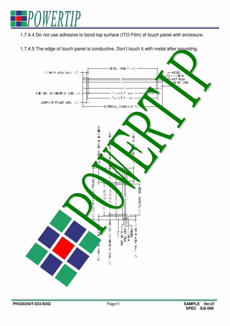
1.7.4.4 Do not use adhesive to bond top surface (ITO Film) of touch panel with enclosure.
1.7.4.5 The edge of touch panel is conductive. Don’t touch it with metal after mounting.

PH320240T-023-I03Q Page12 SAMPLE Ver.01 SPEC Edi.006
2. MODULE STRUCTURE
2.1 Counter Drawing
2.1.1 LCM Mechanical Diagram
* See Appendix
2.1.2 Block Diagram
TP

PH320240T-023-I03Q Page13 SAMPLE Ver.01 SPEC Edi.006
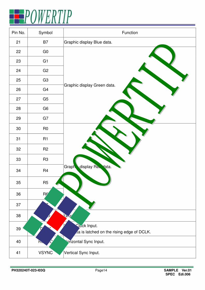
2.2 Interface Pin Description
Pin No. Symbol Function
1 A LED Anode.
2 K LED Cathode.
3 GND Ground.
4 VCI Booster Reference Supply Voltage.
5 ID Note1.
6 VDD Power Supply Voltage.
7 GND Ground.
8 RESB Reset.
9 CSB
Chip select Input:
CSB = L - selected and accessible.
CSB = H - is not selected and not accessible.
10 SCK SPI Clock Input.
11 SDO SPI Data Output.
The data is valid on the falling edge of the SCK signal.
12 SDI SPI Data Input.
The data is latched on the rising edge of the SCK signal.
13 GND Ground.
14 B0
Graphic display Blue data.
15 B1
16 B2
17 B3
18 B4
19 B5
20 B6
PH320240T-023-I03Q Page14 SAMPLE Ver.01 SPEC Edi.006
Pin No. Symbol Function
21 B7 Graphic display Blue data.
22 G0
Graphic display Green data.
23 G1
24 G2
25 G3
26 G4
27 G5
28 G6
29 G7
30 R0
Graphic display Red data.
31 R1
32 R2
33 R3
34 R4
35 R5
36 R6
37 R7
38 GND Ground.
39 DCLK Video Clock Input.
The data is latched on the rising edge of DCLK.
40 HSYNC Horizontal Sync Input.
41 VSYNC Vertical Sync Input.
PH320240T-023-I03Q Page15 SAMPLE Ver.01 SPEC Edi.006
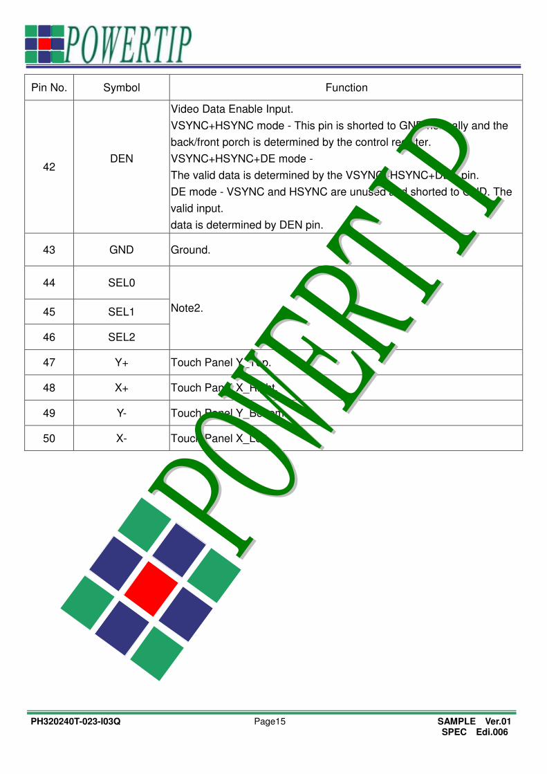
Pin No. Symbol Function
42 DEN
Video Data Enable Input.
VSYNC+HSYNC mode - This pin is shorted to GND normally and the
back/front porch is determined by the control register.
VSYNC+HSYNC+DE mode -
The valid data is determined by the VSYNC+HSYNC+DEN pin.
DE mode - VSYNC and HSYNC are unused and shorted to GND. The
valid input.
data is determined by DEN pin.
43 GND Ground.
44 SEL0
Note2. 45 SEL1
46 SEL2
47 Y+ Touch Panel Y_Top.
48 X+ Touch Panel X_Right.
49 Y- Touch Panel Y_Bottom.
50 X- Touch Panel X_Left.

PH320240T-023-I03Q Page16 SAMPLE Ver.01 SPEC Edi.006
Note1: ID code Circuit
Vendor ID (On FPC, ID resistor as specified in vendor table shall be connected to this pin, and other
side of the resistor shall be connected to GND)
R1=44.2KΩ
Note2: Define the input interface mode

PH320240T-023-I03Q Page17 SAMPLE Ver.01 SPEC Edi.006
2.2.1 Refer Initial code:
//Initial--------------------------------------------------------------
\void Initial_Main(void) // For HX8238-D
MOV DPH,#00H ;Register 0001
MOV DPL,#01H
CALL COM_SER
MOV DPH,#63H
MOV DPL,#00H
CALL DATA_SER
MOV DPH,#00H ;Register 0002
MOV DPL,#02H
CALL COM_SER
MOV DPH,#02H
MOV DPL,#00H
CALL DATA_SER
MOV DPH,#00H ;Register 0003
MOV DPL,#03H
CALL COM_SER
MOV DPH,#01100100B ;DB3 ~ DB0
MOV DPL,#01100100B
CALL DATA_SER

PH320240T-023-I03Q Page18 SAMPLE Ver.01 SPEC Edi.006
MOV DPH,#00H ;Register 0004
MOV DPL,#04H
CALL COM_SER
MOV DPH,#04H
MOV DPL,#C7H ;Parallel 24 bits
CALL DATA_SER
MOV DPH,#00H ;Register 0005
MOV DPL,#05H
CALL COM_SER
MOV DPH,#FCH
MOV DPL,#80H
CALL DATA_SER
MOV DPH,#00H ;Register 000A
MOV DPL,#0AH
CALL COM_SER
MOV DPH,#40H
MOV DPL,#08H
CALL DATA_SER
MOV DPH,#00H ;Register 000D
MOV DPL,#0DH
CALL COM_SER
MOV DPH,#00000010B
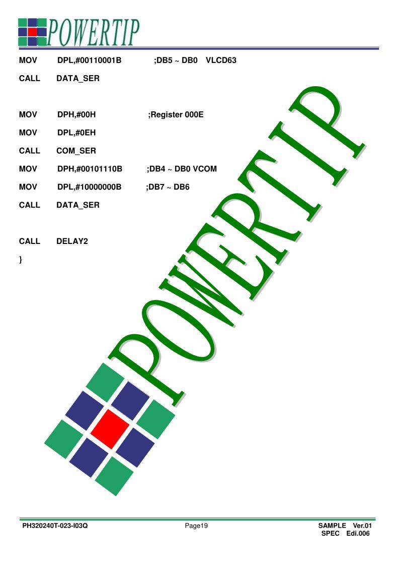
PH320240T-023-I03Q Page19 SAMPLE Ver.01 SPEC Edi.006
MOV DPL,#00110001B ;DB5 ~ DB0 VLCD63
CALL DATA_SER
MOV DPH,#00H ;Register 000E
MOV DPL,#0EH
CALL COM_SER
MOV DPH,#00101110B ;DB4 ~ DB0 VCOM
MOV DPL,#10000000B ;DB7 ~ DB6
CALL DATA_SER
CALL DELAY2

PH320240T-023-I03Q Page20 SAMPLE Ver.01 SPEC Edi.006
2.3 Timing Characteristics
Note:The interface of this module can drive by digital 24-bit data.
VSYNC
HSYNC
DCLK
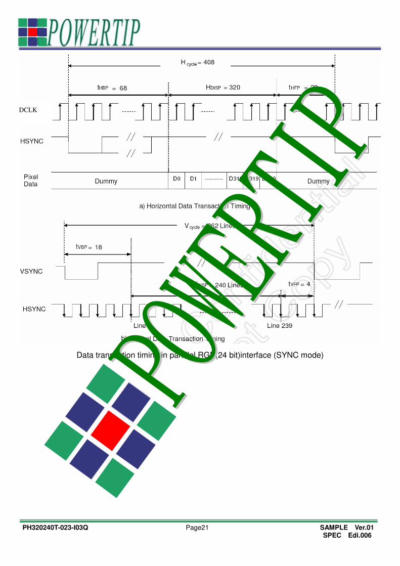
PH320240T-023-I03Q Page21 SAMPLE Ver.01 SPEC Edi.006
Data transaction timing in parallel RGB(24 bit)interface (SYNC mode)
DCLK

PH320240T-023-I03Q Page22 SAMPLE Ver.01 SPEC Edi.006
3. QUALITY ASSURANCE SYSTEM
3.1 Quality Assurance Flow Chart
Item Customer Sales R&D Q.A Manufactur
ing
Product
control Purchase
Inventory
control
Marketing
&
Design
Sample
Approval
Pilot
Run
&
Mass
Product
Ship
Out
OK
Request
Info Survey
Inquiry Project evaluation
Project Validation
Quote OK
NG
Contract
Design check
Sample test
Verification
Sample approval
NG
NG
Pilot run & Reliability test
Verification
Specification preparation
OK
Mass production
Inspection NG OK
Shipment
NG
Ship out
OK

PH320240T-023-I03Q Page23 SAMPLE Ver.01 SPEC Edi.006
Item Customer Sales R&D Q.A Manufactu
ring
Product
control Purchase
Inventory
control
Sales
Service
Q.A
Activity
1. ISO 9001 Maintenance Activities 2. Process improvement proposal 3. Equipment calibration 4. Education And Training Activities
5. Standardization Management
Info Claim
Failure analysis
Corrective action
Tracking
Analysis report

PH320240T-023-I03Q Page24 SAMPLE Ver.01 SPEC Edi.006
3.2. Inspection Specification

PH320240T-023-I03Q Page25 SAMPLE Ver.01 SPEC Edi.006

PH320240T-023-I03Q Page26 SAMPLE Ver.01 SPEC Edi.006
PH320240T-023-I03Q Page27 SAMPLE Ver.01 SPEC Edi.006

PH320240T-023-I03Q Page28 SAMPLE Ver.01 SPEC Edi.006

PH320240T-023-I03Q Page29 SAMPLE Ver.01 SPEC Edi.006

PH320240T-023-I03Q Page30 SAMPLE Ver.01 SPEC Edi.006
PH320240T-023-I03Q Page31 SAMPLE Ver.01 SPEC Edi.006
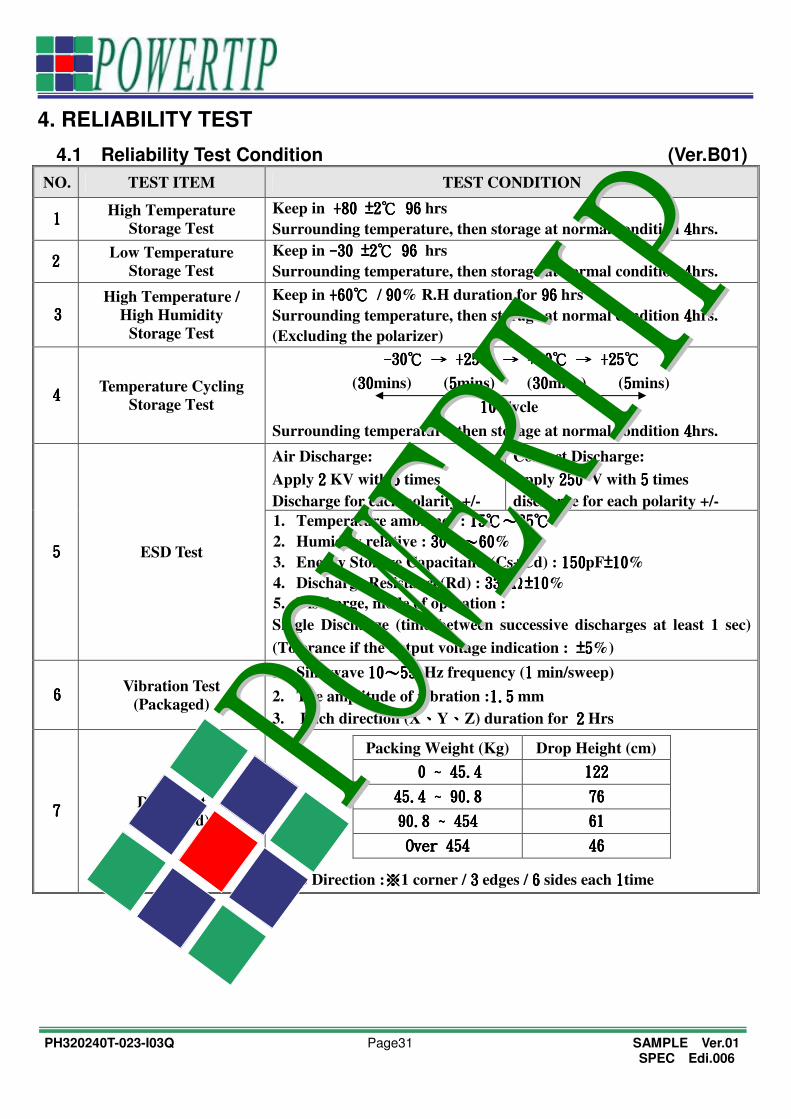
4. RELIABILITY TEST
4.1 Reliability Test Condition (Ver.B01)
NO. TEST ITEM TEST CONDITION
1111 High Temperature
Storage Test
Keep in +80+80+80+80 ±±±±2222 96969696 hrs
Surrounding temperature, then storage at normal condition 4444hrs.
2222 Low Temperature
Storage Test
Keep in ----30303030 ±±±±2222 96969696 hrs
Surrounding temperature, then storage at normal condition 4444hrs.
3333
High Temperature /
High Humidity
Storage Test
Keep in +60+60+60+60 / 90909090% R.H duration for 96969696 hrs
Surrounding temperature, then storage at normal condition 4444hrs.
(Excluding the polarizer)
4444 Temperature Cycling
Storage Test
----30303030 →→→→ ++++25252525 →→→→ +80000 →→→→ ++++25252525
(30303030mins) (5555mins) (30303030mins) (5555mins)
10101010 Cycle
Surrounding temperature, then storage at normal condition 4444hrs.
5555 ESD Test
Air Discharge:
Apply 2222 KV with 5555 times
Discharge for each polarity +/-
Contact Discharge:
Apply 250250250250 V with 5555 times
discharge for each polarity +/-
1. Temperature ambiance : 15151515~~~~35353535
2. Humidity relative : 30303030%~~~~60606060%
3. Energy Storage Capacitance(Cs+Cd) : 150150150150pF±±±±10101010%
4. Discharge Resistance(Rd) : 330330330330ΩΩΩΩ±±±±10101010%
5. Discharge, mode of operation :
Single Discharge (time between successive discharges at least 1 sec)
(Tolerance if the output voltage indication : ±±±±5555%)
6666 Vibration Test
(Packaged)
1. Sine wave 10101010~~~~55 55 55 55 Hz frequency (1111 min/sweep)
2. The amplitude of vibration :1.51.51.51.5 mm
3. Each direction (X、、、、Y、、、、Z) duration for 2222 Hrs
7777 Drop Test
(Packaged)
Drop Direction :※※※※1 corner / 3333 edges / 6666 sides each 1111time
Packing Weight (Kg) Drop Height (cm)
0 ~ 45.40 ~ 45.40 ~ 45.40 ~ 45.4 122122122122
45.4 ~ 90.845.4 ~ 90.845.4 ~ 90.845.4 ~ 90.8 76767676
90.8 ~ 45490.8 ~ 45490.8 ~ 45490.8 ~ 454 61616161
Over 454Over 454Over 454Over 454 46464646

PH320240T-023-I03Q Page32 SAMPLE Ver.01 SPEC Edi.006
5. PRECAUTION RELATING PRODUCT HANDLING 5.1 SAFETY
5.1.1 If the LCD panel breaks , be careful not to get the liquid crystal to touch your skin. 5.1.2 If the liquid crystal touches your skin or clothes , please wash it off immediately by
using soap and water.
5.2 HANDLING 5.2.1 Avoid any strong mechanical shock which can break the glass. 5.2.2 Avoid static electricity which can damage the CMOS LSI—When working with the
module , be sure to ground your body and any electrical equipment you may be using. 5.2.3 Do not remove the panel or frame from the module.
5.2.4 The polarizing plate of the display is very fragile. So , please handle it very carefully, do not touch , push or rub the exposed polarizing with anything harder than an HB pencil lead (glass , tweezers , etc.)
5.2.5 Do not wipe the polarizing plate with a dry cloth , as it may easily scratch the surface of plate.
5.2.6 Do not touch the display area with bare hands , this will stain the display area. 5.2.7 Do not use ketonics solvent & aromatic solvent. Use with a soft cloth soaked with a
cleaning naphtha solvent. 5.2.8 To control temperature and time of soldering is 320 ± 10°C and 3-5 sec. 5.2.9 To avoid liquid (include organic solvent) stained on LCM
5.3 STORAGE 5.3.1 Store the panel or module in a dark place where the temperature is 25°C ± 5°C
and the humidity is below 65% RH. 5.3.2 Do not place the module near organics solvents or corrosive gases.
5.3.3 Do not crush , shake , or jolt the module.
5.4 TERMS OF WARRANTY 5.4.1 Applicable warrant period
The period is within thirteen months since the date of shipping out under normal using and storage conditions.
5.4.2 Unaccepted responsibility This product has been manufactured to your company’s specification as a part for use in your company’s general electronic products. It is guaranteed to perform according to delivery specifications. For any other use apart from general electronic equipment, we cannot take responsibility if the product is used in nuclear power control equipment, aerospace equipment , fire and security systems or any other applications in which there is a direct risk to human life and where extremely high levels of reliability are required.

