technology roadmaps: driving industry...
TRANSCRIPT

Technology Roadmaps: Driving Industry
Collaboration
February 8, 2006Chuck Richardson

1
Topics CoveredTopics Covered
• Overview• Situation Analysis• Highlights from the Product Emulator Groups• Highlights from the Individual Roadmaps• Identified Needs• Paradigm Shifts and Strategic Concerns• Key Recommendations• Major Trends• Innovation Challenge• Closing Pb-free gaps• 2007 Roadmap

2
MissionMission
Assure Leadership of the Global Electronics Manufacturing Supply Chain for the benefit of members and the industry
Software Solutions
Marketing Design Manufacturing OrderFulfillment
Supply Chain ManagementInformation Technology
LogisticsCommunications
Business Practices
Build toOrder
Materials
Components
Customer
Equipment
MaterialsTransformation
Collaborative Design Life Cycle
SolutionsSoftware Solutions

3
MethodologyMethodology
Product Needs
Technology Evolution
GAP AnalysisResearch
Projects
Competitive Solutions
Roadmap
Industry Solution Needed
Academia
Government
iNEMIMembers
Collaborate
No Work Required
Available to Market
Place
Global Industry
Participation Disruptive
Technology

4
Industry Leaders belong Industry Leaders belong –– OEM/EMSOEM/EMS

5
Industry Leaders belong Industry Leaders belong –– SuppliersSuppliers

6
Industry Leaders belongIndustry Leaders belong
Consultants, Government, Organizations & UniversitiesConsultants, Government, Organizations & Universities

7
Attributes of iNEMI RoadmapsAttributes of iNEMI Roadmaps
• iNEMI Roadmap is customer need driven, not technology driven.
• OEM driven Product Emulator Groups (PEGs) start roadmapping process by presenting what they need to remain competitive in the world market.
• Focus of Roadmaps is on process and technology rather than end products.
• Technology Working Groups (TWGs) respond and identify gaps and showstoppers. They do not provide solutions.
• iNEMI Technical Committee prioritizes gaps and forms Technology Integration Groups (TIGs) to close them.

8
2004 Roadmap Priorities 2004 Roadmap Priorities
• Maintain strong linkages with other roadmaps.• Strengthen and realign Product Emulators. • Begin proactively globalizing roadmap. • Expand emphasis on disruptive events (business &
technical).• Expand emphasis on identifying market needs and
business situations. • Increase quantification of needs. • Prioritize Research and Deployment needs.• Increase strategic vision of the roadmap: 2009-2015• Release to industry at APEX 2005

9
Statistics for the 2004 RoadmapStatistics for the 2004 Roadmap
• > 470 Participants• > 220 Companies/organizations• 11 Countries from 3 Continents• 19 Technology Working Groups (TWGs)
(added Sensors)• 7 Product Emulator Groups (PEGs)• Over 1200 Pages of Information• Roadmaps the needs for 2005-2015

10
7 Product Emulator Groups (PEGs)7 Product Emulator Groups (PEGs)
Emulators Characteristics
Portable / Consumer High volume Consumer Products for which cost is the primary driver including Hand held, battery-powered products driven by size and weight reduction
System in a Package Complete function provided in a package to system manufacturer
Office Systems / Large Business Systems
Products which seek maximum performance from a few thousand dollar cost limit to literally no cost limit
Network / Datacom / Telecom Products
Products that serve the networking, datacom and telecom markets and cover a wide range of cost and performance targets
Medical Products Products which must operate within a highly reliable environment
Automotive Products which must operate in an automotive environment
Defense and Aerospace Products which must operate in extreme environments
Yellow = Completely new Emulator Green = Broadened focus

11
19 Technology Working Groups (TWGs)19 Technology Working Groups (TWGs)
Organic Substrates BoardAssembly Customer
RF Components & Subsystems
Optoelectronics
Displays
Energy Storage Systems
Modeling, Simulation, and Design
Modeling, Simulation, and Design
PackagingSemiconductorTechnology
Final Assembly
Mass Storage (Magnetic & Optical)
Passive Components
Product Lifecycle Information
Management (PLIM)
Product Lifecycle Information
Management (PLIM)
Test, Inspection & Measurement
Test, Inspection & Measurement
Environmentally Conscious Electronics
Environmentally Conscious Electronics
Ceramic Substrates
Thermal ManagementThermal
Management
Connectors
Sensors

12
8 Contributing Organizations8 Contributing Organizations

Situation Analysis:MarketTechnologyLegislation

14
The Expanding Digital Product BaseThe Expanding Digital Product Base
New products, enabled by new technologies, are creating a pronounced market shift in the industry:– Blurring of the lines: computers & communications– Cell phone market growth – Emergence of Wireless Products (Bluetooth, 802.11)– Digital Cameras and Personal Entertainment
Systems– Automotive electronics (add functionality of home &
office to your car plus added safety features)– Significant presence in emerging markets is an
imperative (no longer a differentiator).

15
Global Market GrowthGlobal Market Growth
• Production of computers & office products is expected to reach $379Bn in 2004 with growth of 6.2% / year to $483Bn in 2008, accounting for 37% of the electronics market – the largest segment.
• Production of netcom equipment is forecast to be $180Bn in 2004 – about 18% of the electronics industry. Internet use should increase at this segment about 6.3% / year to $230Bn in 2008.
• Portable / Consumer electronics production is reach $183Bn in 2004 increase about 5.1% / year to reach $223Bn in 2008.
• Medical electronics production is expected to be $39.5Bn in 2004(accounting for about 4.9% of the global industry), growing at 4.9% / year to 2008.
• 1.89Bn SiPs assembled in 2004. Forecast for 2008 is 3.25Bn (average growth of 12% / year).
* Market data provided by Prismark Partners, LLC

16
The End of Semiconductor ScalingThe End of Semiconductor Scaling
• The anticipated end to semiconductor scaling c. 2015 will create a major technology shift:
• Implementation of advanced, non-classical CMOS devices with enhanced drive current
• Identification, selection, and implementation of advanced devices (beyond-CMOS)
• Increased need for improved cooling• Potential need for high speed optical
communications at the backplane level• Innovative Packaging for:
– Nano size devices– Giga-function System in Package (SiP)
• Innovation must begin soon to meet the needs!

17
Technology ChangesTechnology Changes
• Growth in silicon device size is slowing
• SiP applications have become technology driver for: – Small components– packaging – assembly processes – high density substrates
• LCD & plasma displays encroaching on CRT market
• MEMS technology is making new capabilities feasible in old and new markets
• Alternative approaches to today’s established data storage technologies will develop over the next decade.

18
Global Environmental LegislationGlobal Environmental Legislation
Legislation impacting the design and recycling of electronic products is being enacted throughout the world:
• Environmental legislation in various product segments requires the electronics industry to share detailed material content data of products and components.
• To meet regional legislative requirements, manufacturers must remove environmental “Materials of Concern,” such as lead.
• The electronics industry is facing producer responsibility (recycling) legislation.

Highlights from the Product Emulator Groups
(PEGs)

20
Automotive PEG Highlights Automotive PEG Highlights
• Reliability – 100,000 miles or 10 years• Harsh Environment becoming harsher• HEV (Hybrid Electric Vehicles) creating new
opportunities For Automotive Electronics• Merging of Automotive and Consumer
Electronics • Ability to respond to environmental legislation • Substrate, component assembly, and IC package
costs should drop: – 30% in the next 5 Years
– 60% in the next 10 Years

21
System in Package PEG HighlightsSystem in Package PEG Highlights
• Broadest adoption of SiP has been for stacked memory/ logic devices & small modules (integrate mixed signal devices & passives for mobile phones).
• SiP provides more integration flexibility, faster time to market, lower R&D cost, & lower product cost for some applications (vs. SOC).
• Infrastructure issues facing SiP implementations include:• Need for low cost higher density substrates• High speed simulation tools for electrical & mechanical
analysis• Wafer level packaging• Lower cost assembly equipment• Improved materials for encapsulation • Skill set and business models vary for EMS/SAS
(Semiconductor Assembly Services)

22
Projected growth for SiPsProjected growth for SiPs
0.00
0.25
0.50
0.75
1.00
1.25
1.50
1.75
2.00
2.25
2.50
2.75
3.00
RF Cell
ular
Digital
WLA
N/Blue
toot
h
Power
Sup
ply
Autom
otive
Imag
e/Disp
layOpt
oelec
tronic
s
Other
SiP
Uni
ts (B
illio
ns)
2003
2007
Handsets51%
Satellite15%
Other4%
Infrastructure30%
Overall SiP Market: 2003 vs. 2007
Sources: Prismark (primary), Deutch Bank, Credit Suisse First Boston, Allied Business Intelligence.

23
Netcom PEG HighlightsNetcom PEG Highlights• Themes for next generation development:
– Common design tools– Common manufacturing / test capabilities – Common component specifications– Leverage across the communications hardware
industry• Telecommunications equipment is facing a crisis: ability
to manage the thermal load in next-generation systems • Need for flexible manufacturing is pervasive across entire
Netcom product portfolio • Most profound paradigm shift is change in supply chain
model, moving from completely vertically integrated companies to nearly completely horizontally integrated companies
• Two strong growth areas will be high-speed Internet access and VOIP (Voice Over IP).

Highlights from the Individual Roadmaps

25
Environmentally Conscious Electronic HighlightsEnvironmentally Conscious Electronic Highlights
To remain competitive, the electronics industry must continue to keep pace with emerging:
– Material restrictions
– End-of life requirements
– Customer preferences for energy efficient products
– Holistic design requirements
– Sustainable business practices.
26
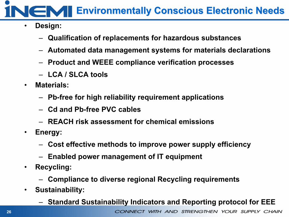
Environmentally Conscious Electronic NeedsEnvironmentally Conscious Electronic Needs• Design:
– Qualification of replacements for hazardous substances – Automated data management systems for materials declarations – Product and WEEE compliance verification processes– LCA / SLCA tools
• Materials: – Pb-free for high reliability requirement applications– Cd and Pb-free PVC cables– REACH risk assessment for chemical emissions
• Energy: – Cost effective methods to improve power supply efficiency – Enabled power management of IT equipment
• Recycling:– Compliance to diverse regional Recycling requirements
• Sustainability: – Standard Sustainability Indicators and Reporting protocol for EEE

27
Board Assembly HighlightsBoard Assembly Highlights
• Board assembly incurs most of the direct-material costs for electronics products and is critical to electronics supply chain
• Identified areas for improvement: - Efficiency and utilization of high mix/low volume lines- Set up times & adoption of factory informationintegration with real time optimization
- Ramps to volume and line flexibility- Qualification processes for materials & process development- DPMO leverage to understand package performance- DFx tools integrated with factory data systems
• Board assembly is being impacted by MEMS, optoelectronics and wireless communications packaging technology development
• Movement of board assembly to low cost areas of the world –primarily China – continues.

28
Assembly Gaps Associated With ComponentsAssembly Gaps Associated With Components
Parameter Definition 2003 2005 2007 2009 2015
Digital Terminals Maximum number of terminals to the board. That are carrying a digital signal per package
800 2900 3200 3500 3500
RF Terminals Maximum number of terminals to the board. That are carrying a RF signal per package
100 200 200 200 200
Maximum Body Size (L x W)- mm 40 52.5 70 70 70 Minimum Terminal Pitch BGA Pitch of the I/O (mm) 1.27 0.80 0.80 0.65 0.50
Minimum Terminal Pitch CSP Pitch of the I/O (mm) 0.65 0.50 0.40 0.40 0.30
Number of stack die Maximum number of stacked die in a package 4 7 8 8 8
Number of die in SiP max
Maximum number of stacked or unstacked die in a package 8 10 12 12 12
Minimum Component size
Minimum component size used in a package by type 0201 0201 01005 01005 01005
Embedded Passives N/A Few YES YES YES YES
MSL Level Moisture sensitivity level per IPC that packages are qualified 3 2 2 2 2
Max Reflow Temperature
Common reflow temperature for multi die packages. – deg C 250 260 260 260 260
Thermal conductivity critical 80% 85% 90% 90% 90% Low temperature capability <5% <5% <5% <5% <5% Pre-applied <1% 3% 5% 20% 30% Die Attach Materials
Matched CTE capability 0% 5% 7% 15% 25%
Key Current Capability
In Development Research Needed

29
Interconnection Substrates HighlightsInterconnection Substrates Highlights
• Area array components driving wiring density increases in organic substrates
• New high speed requirements demand Z axis control, signal integrity and EMI design considerations
• Integral passives are needed for both wiring density and electrical performance
• Cost expectations of iNEMI emulators may be difficult for European & North American fabricators.

30
Packaging HighlightsPackaging Highlights
• Packaging costs have become a larger part of I/C costs
• Impact of packaging is increasing, but R&D investment is not
• Packaging has become a major competitive factor due to: – rapid growth in wireless – complex consumer products
• Emerging device technologies driving new packaging requirements
• Major challenge: modeling/simulation of mechanical, thermal & electrical performance of the entire chip, package & heat removal structures as a system.

Identified Needs

32
Design Technology Design Technology -- NeedsNeeds
Design & simulation tools are main roadblocks to more rapid introduction of new technologies:
– Mechanical & reliability modeling
– Thermal & thermo-fluid simulation
– Co-design of mechanical, thermal & electrical performance of the entire chip, package & associated heat removal structures
– Simulation tools for nano devices & materials
– Improved design tools for emerging technologies like embedded passives & optoelectronic PWBs
– Integrated design & simulation tools (circuit, EM, thermal, mechanical, manufacturing, etc.) for higher functionality in mixed-mode wireless chips & modules.

33
Manufacturing Technology Manufacturing Technology -- NeedsNeeds
• Improved stencil technology or paste dispensing
• Cost effective under fill process including rework
• Equipment to close cost gap between flip chip & SMT placement
• Reconfigurability for final assembly
• SMT compatible optical assembly processes with accuracies < 10 µm
• Test procedures for optical components & electro/optical systems
• Analog test including scan and self-test technology.

34
Optoelectronics Technology Optoelectronics Technology -- NeedsNeeds
• Development of optical polymeric materials for improved multimode data transmission
• Development of multi-frequency chip-to-chip interconnections
• Combined processing of high frequency and micro optical components
• Development of optical connectors and package interfaces
• Wafer level packaging for optoelectronic systems• Cost-effective packaging for long wavelength single
mode VCSELs.
35
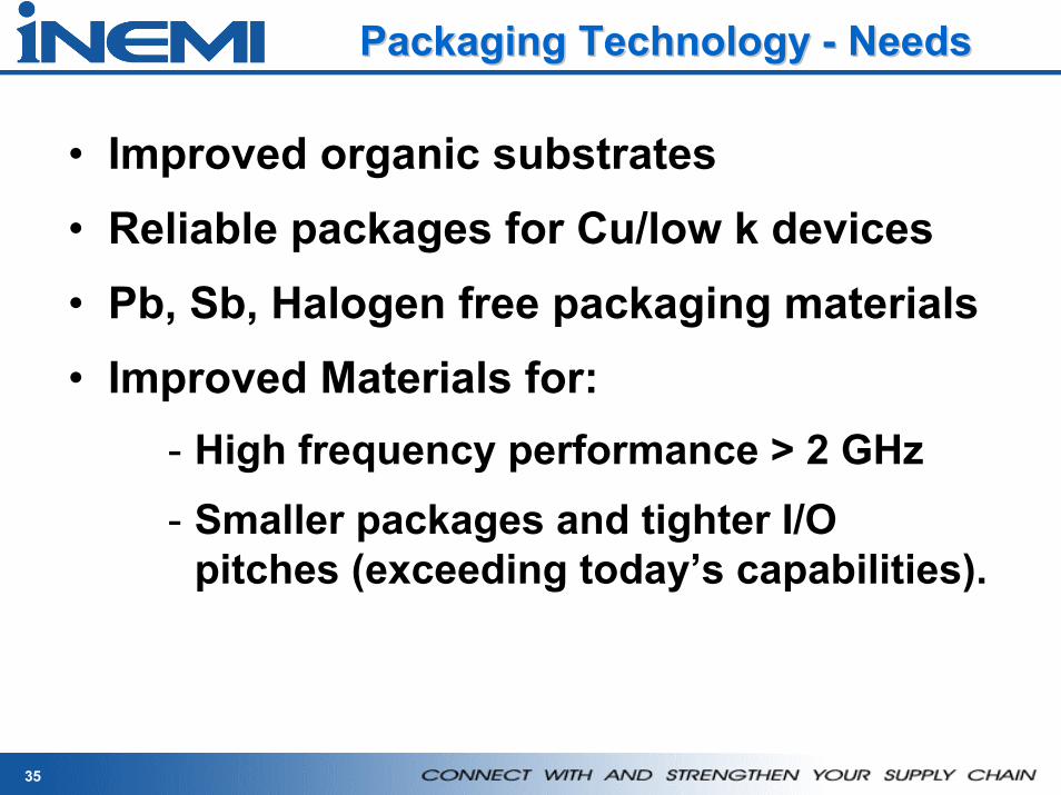
Packaging Technology Packaging Technology -- NeedsNeeds
• Improved organic substrates• Reliable packages for Cu/low k devices• Pb, Sb, Halogen free packaging materials• Improved Materials for:
- High frequency performance > 2 GHz- Smaller packages and tighter I/O
pitches (exceeding today’s capabilities).

36
Component/Subsystem Technology Component/Subsystem Technology -- NeedsNeeds
• Improved performance & reduced leakage in low power applications
• Medium power, low-loss, high-selectivity RF filters
• Improved optoelectronic subcomponents and component integration
• Low cost, high volume optical connectors
• In-circuit test technologies that are incorporated into the build process
• Cost & performance models:
– Evaluate trade offs between embedded passives and 01005 components
– Evaluate optical versus copper interconnection

37
Supply Chain Integration Supply Chain Integration -- NeedsNeeds
• Material Traceability through Product Life Cycle for:
– Environmental and Medical Regulations
– Automotive and Military Requirements.
• Further Integration of design chain/supply chain to reduce costs and improve performance throughout the product life cycle:
– Understanding customer needs (moving target)
– Critical information flow
– Timely decisions that optimize performance of entire chain rather than one node.

Paradigm Shifts & Strategic Concerns

39
Paradigm ShiftsParadigm Shifts
• Convergence of broadband communications and digital technology has increased product opportunities while creating market uncertainty:– What is the right combination of functions?– Which companies/services will win?– Trends are beginning to emerge
• System in Package functional modules are speeding the design of new portable and office system products and reducing risk to the OEM. Product examples:– Bluetooth – WiFi (802.11b,a,g) – GSM (Global System for Mobile Communication )

40
Vision of the Evolution of SiPVision of the Evolution of SiP
Source: Professor Rao Tummala, Georgia Institute of Technology-Packaging Research Center.

41
Potential Disruptive TechnologyPotential Disruptive Technology
• Rapid introduction of complex, multifunctional new products to address converging markets favors development of functional, modular components (e.g. SiP)
– Increases flexibility & shortens product design cycle & places test burden on module producers
– This architecture allows for MEMS device construction with a variety of new applications in fuel cells & life sciences (DNA/blood testing)
• Wireless applications are an important driver for semiconductor products & technologies and may stimulate disruptive solutions
• Nanotechnology has the potential to be a very disruptive technology during the period covered by the roadmap
• New energy technologies that may cause disruptive opportunities include fuel cells and high power batteries for hybrid electric vehicles.

42
Strategic ConcernsStrategic Concerns• Given flow of technology & manufacturing between
countries, many key component industries are looking for alternative business strategies to maintain leadership
• Innovative approaches to Enterprise IT & supply chain management which increase ROI in a predictable way
• EMSs are being asked to provide R&D leadership while keeping overhead low – this may not be a viable business strategy
• The materials supply base does not have adequate demand (at high enough margins) to drive many of the needed new materials
• Impact of Environmental Compliance on financials, reliability, & IT infrastructure
• Reliability of less mature material systems

Key Recommendations

44
Key Recommendations Key Recommendations iNEMI Technical Projects• Establish a SiP TIG to address process, materials, equipment, &
reliability gaps.• Establish a project in the interconnect arena that explores dimensional
stability of materials used in PWB manufacturing (driven by fine pitch and microvia technology).
• Establish a research project on new organic materials with improved properties for electronics packaging.
Design• Develop co-design capabilities of mechanical, thermal, and electrical
performance of the entire chip, package, & heat removal structures. • Develop improved design tools for emerging technologies like
embedded passives and optoelectronic PWBs.
Manufacturing Technology• Develop automated printing, dispensing, placement, and rework
equipment capable of the pitch requirements for SiP package assembly at current process speeds.

45
Key Recommendations Key Recommendations Materials Development• Low cost, higher thermal conductivity, packaging materials, such as
adhesives, thermal pastes, and thermal spreaders. • New interconnect technologies deploying nano-materials to support
decreased pitch and increased interconnect frequencies.• Characterize & improve reliability of material systems.
Energy and the Environment• Development & implementation of scientific methodologies to assess
true environmental impacts of materials and potential trade-offs for alternatives.
• Develop a common, straightforward definition of sustainability that:– Can be applied quantitatively at the business level – Can be easily communicated to stakeholders – Can be used to set targets
Technology Development• Thermal Management of high power densities• Develop reconfigurable or adaptive radio transceivers.

46
Some applications and benefits of Nanotechnology Some applications and benefits of Nanotechnology (Motorola)(Motorola)
Nano Composites: stronger, tougher, stiffer, lighter materials (adhesives, structural,thermal, electronic, optical functionality)
Nano displays: Large, lower cost and brighter displays based on embedded carbon nanotubes
Nano sensors: smaller, more sensitive Nano scale sensors for bio, optical, chemical and physical sensingNano antennas: Nano scale fractal antennas for multiple spectra and broadbandNano power: High capacity power sources (storage, conversion, advanced fuel cells, photonic energy), parasitic energy harvesting, nanobiotech related functionality

Major Trends

48
Major Trends Major Trends –– Current & FutureCurrent & Future
• Environmental considerations will expand– RoHS/WEEE is the beginning– Significant impact to supply chain/information needs – Design for Environment/Sustainability – Defensive posture has reduced industry’s influence on
regulations• Mfg. migration to low cost regions continues
– Some corrections seen due to security/logistics costs– Commodity design is following
• SiP is a major trend in portable products– Infrastructure issues need attention– Could find use in other sectors where mixed IC technologies
are used • Lack of integrated design/simulation tools is:
– Delaying new technology adoption – Impacting product time to market

49
Major Trends Major Trends –– Current & FutureCurrent & Future• The predicted end of semiconductor scaling
could have major implications:– Non classical CMOS– Beyond CMOS– Increased thermal challenges– Significant impact to packaging/interconnect
• Nanotechnology has the potential to dramatically effect electronics:– Materials– Displays– Sensors– Power
• Innovation thrusts have become very fashionable– Many are policy oriented– iNEMI can add value by creating research vision.

Innovation Challenge

51
Closing Needs through Research:Closing Needs through Research:A Challenge to be StrategicA Challenge to be Strategic
• A number of Needs have appeared since the 1994 Roadmap.
• We need be innovative and look for disruptive business & technology Solutions to these Needs.
• We need to identify the research areas that would provide the technology Solutions to these Needs. For example:– Material Needs: Nanomaterials– Manufacturing Processes: flexibility and
reconfigurability– Design: Rapid Modeling of Complex Systems

52
The Next Great ChallengeThe Next Great ChallengeThe End of Semiconductor ScalingThe End of Semiconductor Scaling
• The anticipated end to semiconductor scaling will create a major technology shift in the industry:
• Implementation of advanced, non-classical CMOS devices with enhanced drive current
• Identification, selection, and implementation of advanced devices (beyond-CMOS)
• Increased need for improved cooling• Innovative Packaging for giga-function systems
• Innovation must begin today to meet these needs• iNEMI Innovation Leadership Forum - 9/15, 9/16
• Convened key industry, government, university and business leaders
• discuss issues and develop a Research Vision that will focus investments on the right topics.

53
Innovation Forum ResultsInnovation Forum ResultsMajor Accomplishments:1. Identification and participation of leaders in
electronics manufacturing innovation.2. Great descriptions of all levels of innovation (i.e.
identification of "next big things", some level of supply chain technology related to electronics manufacturing, and innovation process/business model strategies).
3. Identification of shortcomings/limitations in government policy (related to innovation).
Next steps:1. Create Innovation/Research Vision2. Communicate to Research Stakeholders3. Develop plan for iNEMI “next big thing”.

54
Electronic Materials
$62Bn
ActiveComponents
$197Bn
IC AssemblyServices$6.2Bn
PassiveComponents
$143Bn
EMSAssembly$110Bn
2003Finished
Equipment$950Bn
VALUE CREATION IN THE SUPPLY CHAINVALUE CREATION IN THE SUPPLY CHAIN
Typical Companies
Sumitomo Bakelite,DuPont, Ablestik
Intel, STMicro,LSI Logic
Amkor, ASE, SPIL
Tyco, Molex,AVX, Sharp
Solectron, Sanmina-SCI,
Flextronics
Dell, HP, Cisco,Nokia, Teradyne,Visteon, Siemens
GrossMargin
30% 40% 12% 25% 7% 30%
OperatingMargin
10% 15% 8% 8% 2.5% 8%
R&D 7% 15% 2% 5% <1% 8%MarginValue
$6Bn $30Bn $0.5Bn $11Bn $3Bn $76Bn
R&DValue $4Bn $30Bn $0.1Bn $7Bn <$1Bn $76Bn
N94.034bes-chain
%TotalR&D 3% 25% 64%
Prismark

55
Wake Up Call: Vision Focus AreasWake Up Call: Vision Focus Areas
• Need 2005 Sputnik equivalent of “Wake up” or rallying call. Must have social value. Could it be:
– Energy: reduce imports by P% in N years…..
– Security/Safety: post 9/11….
– Health Care: ex. 30min of paperwork for every hour of patient care, 98K avoidable deaths/yr
– Data/Telecom: from New Orleans breakdown • Define national goals with specific timelines.• Rallying call with a face• Credible spokesperson should make the call
– Credibility issue with Mars landing vision• Must convince 5th precinct – the public

56
Guiding principles in the new Guiding principles in the new innovation modelinnovation model
Monolithic Product Development
Global Product development networks
Top-down control Symbiotic partnershipsGovernance
Corporate ethos Not invented here Best from anywhere
Attitude toward IP Own and protect Share and expand
Innovation processes Rigid Flexible
Success metrics Patents Customer experience
Role of customers Passive users Active co-innovators
Source: Forrester Research-Navi Radjou

Pb-free Assembly: Closing Gaps

58
Closing Gaps: Environmental Closing Gaps: Environmental Projects to Eliminate Pb SolderProjects to Eliminate Pb Solder
• 1998 Roadmap identified the technology gap.
• Phase I project developed the alloy, process, components and reliability from 1999-2002.
Results:
– The iNEMI efforts accelerated the establishment of SAC alloys as the standard and reduced the effort in each member company.
• Phase II projects have expanded the technology base to include assembly and rework of large complex PWB assemblies.

59
Closing Gaps: Environmental Closing Gaps: Environmental Projects to Eliminate Pb SolderProjects to Eliminate Pb Solder
• 2002 Roadmap identified a number of business Issues to convert to a Pb-free supply chain.
• Five Phase III project teams have addressed these supply chain transition issues.
• Phase IV projects are being established to close recently identified technology gaps:– Wave/selective solder– Mixed assemblies (Pb-free BGA’s in a SnPb assembly
process)– Pb-free surface finishes– Pb-free Rework Optimization– Pb-free DPMO– Pb-free Nano-solder– High Reliability RoHS Compliance

60
Lead-Free AssemblyChair: Edwin Bradley, PhD Motorola
Co-Chair: Rick Charbonneau
Environmentally Conscious Electronics (ECE) Technology
Integration Group (TIG)
Tin Whisker ModelingChair: George Galyon, IBMCo-Chair: Maureen Williams, NIST
Tin Whisker Users GroupChairs: Joe Smetana, Alcatel
Richard Coyle, Lucent
Lead-Free Assembly & ReworkChairs: Jerry Gleason, HP
Charlie Reynolds, IBM
Lead-Free Assembly & ReworkChairs: Jerry Gleason, HP
Charlie Reynolds, IBM
RoHS Transition Task GroupChair: Dave McCarron, DellProjects: Component Supply Chain Readiness
Chair: John OldendorfComponent and Board Marking
Chair: Vivek Gupta, IntelAssembly Process Specifications
Chair: Frank Grano, -SCIMaterials Declarations
Chair: Nancy Bolinger, IBM
Complete
Pb-free Wave Soldering Chair: Denis Barbini, Vitronics Soltec
Co-chair Paul Wang, Microsoft
Complete
Complete
Pb-free Rework OptimizationChair: Jasbir Bath, Solectron
Halogen-freeChair: Steve Tisdale, Intel
RoHS High RelChair: Mike Davisson, AgilentCo-Chair: Joe Smetana, Alcatel
Tin Whisker Accel. TestsChair: Valeska Schroeder, HPCo-Chairs: Jack McCullen, Intel
Mark Kwoka, Intersil

61
Board Assembly ProjectsBoard Assembly Projects
Board Assembly TIGChair: Tom Pearson, Intel
Pb-Free BGAs in SnPb Assemblies
Chair: Robert Kinyanjui, Sanmina-SCICo-chair: Charan Gurumurthy, Intel
Pb -Free Assembly Substrate Surface Finishes
Chair: Keith Newman, Sun Microsystems, Co-chair: Charan, Gurumurthy, Intel
SMT Reel Labeling
Chair: Patrick Figueroa, Delphi Electronics & Safety
Pb-free Nano-solder
Chair: Andrew Skipor, Motorola
Pb-free DPMO
Chair: Andrew Dugenske, Georgia Institute of Technology

2007 Roadmap

63
Roadmap Cooperation with IPCRoadmap Cooperation with IPC
• Formal 2007 iNEMI Roadmap cycle began at SMTAI, 9/30/05 .
• Product Emulator Group’s (PEG’s) started the process by reviewing emulators and suggesting changes.
• IPC is working with iNEMI to continue to improve Interconnect Substrate - Organic chapter.
• First IPC Roadmap meeting held 11/13/06 in Mesa Arizona. – iNEMI was represented by Chuck Richardson.
• 2007 iNEMI Roadmap kick-off meeting held 2/6,7/06 in conjunction with APEX 2006.– IPC was represented by Jack Fisher.

64
2007 Roadmap Schedule2007 Roadmap Schedule• 3Q2005: Select Product Sector Champions, teams and refine data
charts• 3/4Q05: Product Sector Champions Develop Emulators
– September 6, 2005 – Teleconference with P.E. Group Chairs– September 30, 2005 Roadmap Kick-off with PEG/TWG/TC at
SMTAI– November 16, 2005 European Kick-off at Productronica– December 2005 review meeting with TC on PEG Emulators
• 2004 chapter, format, Exec. Summary mailed to each TWG chair (Word 6.0) 1/4/2006
• Organizing Teleconference with TWG Chairs 1/23/2006• February 2006 PEG Workshop/TWG Kick-off at APEX Meeting in
Anaheim:– Product Sector Tables Nearly Complete – Chapter Draft Written– Cross Cut Issues Addressed
• May 8, 2006 Telecon With TWG Chairs • May 17, 2006 – Open Roadmap Presentation in Herndon, VA

65
2007 Roadmap Schedule 2007 Roadmap Schedule -- ContinuedContinued• May 18, 2006 – TC Roadmap Highlights Meeting in Herndon• May 18, 2006 – TWG/PEG Cross Cut Meeting, Herndon • May / June 2006 - Roadmap Workshop – Europe• June 27-30 - Roadmap Workshop HDP ’06 Shanghai• July 1, 2006 – TWG Drafts Due for TC Review• August 9, 2006 – TC Face-to-Face Review with TWG Chairs
in Kokomo (Delphi)• September, 2006 – Council Review of Key Issues and
Preliminary Summary @ SMTAI, Final Roadmap Chapters Due 9/22/06
• October 31, 2006 – Edit, Prepare App. A-D, Exec. Summary • November 20, 2006 – Go To “Press” • December 4, 2006 – Ship to Members • Feb, 2007 – Industry Release at APEX

CostCost--Effective Supply Chain Effective Supply Chain Technology DeploymentTechnology Deployment
• iNEMI roadmaps/gap analyses help set the agenda for electronics industry.
• iNEMI is providing the Leadership required to work emerging technologies/opportunities.
• iNEMI is Leveraging R&D investments (academia & government) to address industry’s agenda.
• Projects lead to improved deployment (faster, better, lower cost) created across supply chain.
• Standards efforts (with IPC, EIA, IEEE, and RosettaNet) are encouraging broad utilization of emerging technologies/solutions.

67
www.inemi.orgwww.inemi.orgEmail contacts:Email contacts:
Chuck Richardson Chuck Richardson
Chuck.Chuck.richardsonrichardson@@inemiinemi.org.org
Bob PfahlBob Pfahl
[email protected]@inemi.org