the-eye.euthe-eye.eu/public/books/electronic archive... · foreword...
TRANSCRIPT

€"'
DATA BOOK 1965-66

J
J)
1a sum
Mullard Pocket Data
Book
1965/66 Edition
'65•
Woisia:
tLS iLSii\
10it.-
Mullard Ltd.,
MuHard/House, Torrington Place, London, W.C.I

FOREWORD
The Milliard Pocket Data Book is presented so asto provide easy reference to the valves, cathode raytubes, semiconductor devices and components in theMullard range with which the Service Engineer is
most concerned. It is suggested that previous editionsof the Pocket Data Book are retained for reference toobsolescent types, a list of which is contained in this
edition. Information on these types may also befound in the original edition of the Mullard Main-tenance Manual.
The Equivalents List may be removed from themain book if desired.
The Data Book has been prepared by CentralTechnical Services, Mullard Ltd., who also publishthe Mullard Technical Handbook on a subscription
basis. Details of this service and further data onindividual types may be obtained from this depart-
ment.
CONTENTS
Page
Foreword.... g^yS -ELECTOR . 2
The latest Mullard intro£i$&$sJ^L* *.\ 4
Top Ten Plus. . ^lOStTELEVISIONg
Mullard Technical PubUcSSis. ... 7
Symbols and abbreviations ..... 8
Valve, cathode ray tube and semiconductor
data section .10List of earlier types and types not in common use 10
Component data section 80
Comprehensive valve, cathode ray tube and
semiconductor equivalents list . . .Insert
Page 2
Page 3
rTHE LATEST MULLARD
INTRODUCTIONS
AC128/ACI76—These two transistors form part of the newMullard harmonious range of audio transistors. When usedas a complementary output pair they make possible the designof transformerless amplifier circuits, and 3W output (speechand music) are obtainable in Class 'B* operation in mains-powered equipment.
AUI03—A television line output transistor for transistorised
portable television receivers. The AU103 has been devel-
oped for use in conjunction with the efficiency diode BY1 1 8,
BY118—The BY118 efficiency diode has been designed for use
with the AU103 line output transistor and is recommendedfor use in transistorised portable television receivers. Thediode has reverse voltage rating of 300V and a current rating
of 14A associated with fast switching characteristics andlow forward voltage drop,
BYX10—A high voltage silicon diffused rectifier enclosed in aplastic encapsulation and designed for use in transistor
television receivers. It is employed to produce h.t. supplies
(from the line output stage) for the first anode and the
focus electrode of the picture tube, and also an h.t. supply
for the video output stage.
A47-14W/A59-15W—In collaboration with leading setmakers,Mullard have deepened the tint of the faceplates on the
current range of television picture tubes. This gives
improved picture contrast ratio and reduces reflections
caused by ambient room and window lighting.
'Radiant Screen' tubes are marketed under the following
new type numbers : 1 9-inch A47- 14W and 23-inch A59- 1 5W.These were formerly AW47-91 and AW59-91 respectively.
BF109—The BF109 is a video output transistor manufacturedby the silicon mesa technique. It is designed for use in
hybrid and fully transistorised television receivers to meetthe requirements of high voltage rating and dissipation withlow feedback capacitance.
* ss^acf& fSWffl*
9*
Page 4 Page 5
TOP TEN PLUS
This Data Book contains informationon over 100 types of valves, however it
should be remembered that the bulk ofvalves in use is made up by a comparativelyfew popular and regularly stocked types.
This is why Mullard introduced the TOPTEN PLUS, to enable you to keep a compactstock of valves which will meet most of yourservicing requirements.
The Mullard Top Ten Plus can bepurchased through your wholesaler in con-venient sleeves of three. Place a regular
stock order now with your supplier for the
following types
:
ECC82 EY86 PCL83
ECL80 PCC84 PL81
EF80 PCF80 PY33
EY51 PCL82 PY81
ALWAYS ORDER MULLARD VALVESBY NAME AS WELL AS TYPE NUMBER
Page 6
MULLARD TECHNICAL PUBLICATIONSAll of the following publications are available through
normal trade channels or direct from Home Trade SalesDivision, Mullard House, at the usual trade discount. Whenordering only one copy direct from Mullard Limited, the costof postage and packing should be added.
THE MULLARD MAINTENANCE MANUAL-SECOND EDITION
A "must" for the service department, this Manualcontains information on all current replacement types ofvalve, tube, and semiconductor with a continuous supplemen-tary data sheet service. Retail price 16s. Od, Postage I/- extra.
TRANSISTOR RADIOS—CIRCUITRY AND SERVICINGContents include a simple explanation of how a transistor
works, the complex manufacturing processes involved inproducing transistors, care and methods of repairing printedwiring boards, varioi*titMft ti"tvfa.?
il/iifM'ii
r": servicing,test equipment, eta. K3tiirp?ic*«fcuDuJx^^fe6d. extra.
/ MM FLEET Sf„r ^EMBERTON.
MULLARD cfirec^&CStSO AMPLIFIERSMullard high-qu^td audio circuits— this book has already
proved itself a best-Seller arhohg-aiU amateur radio and hi-fi
reproduction enthusiasts. Retail price 8s, 63. "Postage 6d.extra.
REFERENCE MANUAL OF TRANSISTOR CIRCUITSDescriptions ofmore than 60 circuits covering both domes-
tic and industrial applications. Retail price 12s. 6d. Postage1/- extra.
Page 7

SYMBOLS & ABBREVIATIONS
1 . Base and Connections
a Anode.B Base.C Collector.E Emitter,
f Filament.ff Filament positive.
i" Filament negative.let Filament centre tap.
I Grid.h Heater.hct Heater centre tap.
hUp Heater tap.
1C Internal connection (must not be connected externally)
k Cathode.M Metallising (external) or base sleeve.
NC No connection.NP No pin.
s Internal shield.
t Fluorescent screen or target.
NOTE 1 —In valves having more than one grid, the grids are
distinguished by numbers: gl, g2, etc., gl being the
grid nearest the cathode,
NOTE 2—In multiple valves, electrodes of the different sections
are distinguished by adding one of the following
letters
:
Diode ... , dTriodc ... ... ... ... ... - t
Pentode PHexode ...
HeptodeOctode ...
Thus the grid of the triode section of a triode pentodeis denoted by gt.
NOTE 3—Two or more similar electrodes which cannot bedistinguished by any of the above means may bedenoted by adding one or more primes to indicate ofwhich electrode system the electrode forms a part.
Thus, the anode of the first diode in a double diods
yalve is denoted by a'.
Page 8
SYMBOLS & ABBREVIATIONS
l. Characteristics
fgcgmlaia(pk)max. ...
Ia(av)max. . .
.
IcICBOIfIg2Ig2+g4Ihlout max.It
pa max.Ptot max.P.I.V. max. ...
PoutraRaTambVava(pk)max, ...
VbVCEVCBVf „Vgl fVg2Vg2+g4Vhvh— k(pk)inax.
hfe
hFEL
Oj-ambGj-case
Frequency.Conversion conductance.Mutual conductance.Anode current.Maximum peak anode current.Maximum mean anode current.Collector current.Collector cut-off current (common base).Filament current.Screen-grid current.Screen-grid current (frequency changers).Heater current.Maximum output current.Target current (tuning indicators).Maximum anode dissipation.Maximum total dissipation.Maximum peak inverse voltage.Power output (for 10% distortion).Anode impedance.Anode load.Ambient temperature.Anode voltage.Maximum peak anode voltage.Supply voltage.Collector-emitter voltage.Collector-base voltage.Filament voltage.Negative grid voltage.Screen-grid voltage.Screen-grid voltage (frequency changers),I Icatcr voltage.Maximum peak voltage between heater and
cathode.Small signal current amplification factor
(common emitter).Large signal current amplification factor
(common emitter).Amplification factor.
Thermal resistance.
Page 9
DATA SECTION
LIST OF EARLIER TYPES AND TYPESNOT IN COMMON USE
AZIAZ31AZ41
CCH35CL33
DA90DAC32DAF91DCC90DF33DF64DF66DF9!DF92DF97DK32DK40DK91DL33DL35DI.64DL68DL92DL93DM70DM71DW4-350DW4-500
EA50EAC91EAF42EB34EB41ERC33EBC90EBC91EBCH12
Page 10
EBL21EC52EC90HC91EC92ECC32ECC33ECC34ECC35ECC40ECC91ECH3ECH21ECH35EF9EF22EF37AEF39EF40EF41EF42EF50EF55EF92EF93EF94EF9SEK90EL32EL33EL36EL37EL38EL4IEL42EL83EL85EL86EL90EL91EL82IEM34EY81EY91EZ35EZ40EZ4IEZ90
{See Foreword)
FC4FW4-50OFW4-SQ0
GZ30GZ32GZ33GZ37
1W4-350JW4-500
MW6-2MW22-16MW31-74MW41-1MW43-43
OA47OA71OC57OC58OC59GC60OC65OC66
PC95PEN4DDPENA+FL33PL38PY31PY32PY80PZ30
TY86F
UAF42UB41
UBL2IUC92UCH21UF42UF85UF86UL44UL46UM4URICUY1N
VP4B
IC5G/GTIH5G1N5G3Q5GT5U4G5V4G5Z4GT6A8G6F6G6J5G/GT6SK7GT6SN7GT6V6G/GT6X5GT12J7GTJ2K7GT12Q7GT12SK7GT12SN7GT25A6G25L6GT25Z4G35Z5GT4250L6GT80
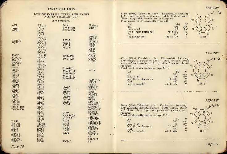
47cm (19in) Television tube. Electrostatic focusing,110° magnetic deflection angle. Metal-backed screen.
Glass safety shield bonded to the faceplate.
F'inal anode cavity connector type CTS.
Vh G-3
Ih 300Va2 4- a4 16
Va3 (focus electrode) to 400Val 400Vg for cut-off -40 to -77
A47-13W
2+ a4
A47-18W
47cm (I9in) Television tube. Electrostatic focusing,110° magnetic deflection angle. Metal-backed screenand reinforced envelope. A separate safety screen is notrequired.Final anode cavity connector type CTS,
Vh 6-3
Ih 300Va2 + a4 IS
Va3 (focus electrode) to 400Val 400Vg for cut-off -40 to -77 B8II
59cm (23in) Television tube. Electrostatic focusing,110° magnetic deflection angle. Metal-backed screen
and reinforced envelope. A separate safety screen is notrequired.
Final anode cavity connector type CTS.
VhIhVa2 4- a4Va3 (focus electrode) to 400Val 400Vg for cut-off -40 to -77
A59-11W
^V a4
Page 11
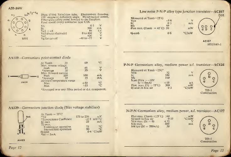
A59-16W
<fea2*°4
59cni (23in) Television tube. Electrostatic focusing.
lit) magnetic deflection angle, Metal-backed screen.
Filter-glass s;ifety panel bonded to the faceplate.
Final anode' cavity connector type CT8.
Vh fr3 V]h MO mAVa2 : a4 IS kVVa3 (focus electrode) to 400 VVal 400 VYg for cut-off -40 to -77 V
Low noise P-N-P alloy type junction transistor—AC107Dot
Measured atTamb — 25"CVcb -5-0
Ic 0-3
hfe 60Ptot max. (Tamb - 45 C) 50
Oj-amb 0-6
VroA
mW"C/mW
AC107S02/SB3-2
AA119—Germanium point-contact diode
At Tamb 25 60 "CMax. reverse voltage
Peak 45 45 VAverage 30 30 VMax. forward currentPeak 100 100 mA
*Avcrace 35 15 cnAAmbient temperature range
Max. -| 60 "CMin. -55 cc
Averaged over any 50ms period or d,c component.
P-N-P Germanium alloy, medium power a.f. transistor
—
AC126
Measured at Tamb
-
; 25C5
Vcb 32Ic 100hfe 180IClio (Vco = -10V
be,-- OmA) <I0
Ptot. max. (Tj = 75"C) 500Oj-amb in free air 0-3
VmA
uAmW
°C/mW
AA129—Germanium junction diode (Bias voltage. stabiliser)
r~>At Tamb = 25
rCDot Vd 175 to 230 raV/ Temperature Coefficient -2-3 mV/°C
nrf Id max. 20 mAyy Tj max.
Vh- Continuous operation 75 °C
zi Intermittent operation 90 °C
jL Oj-amb 0-4 °C/mWId = 5mA
AAI29
Page 12
N-P-N Germanium alloy, medium power, a.f. transistor—AC127
Ptot max. (Tamb <:25 C) 340 mWOj-amb in free air 0-37 c C/mWVeil max. (If: — 0) -f.32 Vk'M max. 500 mAhi E typ (Ic = 500mA) 50
TO-tConstruction
Page 13

AC128, 2-AC128—P-N-P Germanium alloy high gain transistor.Class A and B output stages
TO-lConstruction
Measured at Tamb — 25°CVci! (Ie = 0)Icm max.hFE (Ie = 300 mA,VCB = 0)
Icbo (Yen = -10V,Ie = 0)
Ptot max.Gj-amb in free air
-321
60 to 175
10700
0-29
VA
nAmW°C/mW
AD14G—P-N-P power junction transistor
ePtot max. (Tease <375°C) 35 WOj-case 1-5 °C/WVcb max. (Ie = 0) -55 V*1c(av) max. 3-0 AKfelOc = 1A) 30-100•Averaged over any 20ms period.
AF102—P-N-P alloy diffused junction transistor
interlead shieldand metal case
Ptot max. (Tamb <45°C)Oj-ambVCB max. (Ie = 0)
5006
-25
mW°C/mW
V
(a b r c\ooo ol
Icm max.it typ(lE = POmA,Vcb = -12V)
Cobs typ (Ik = 1'OmA,Vcb = -12V)
hfc min. (Ie ^ 10mA,Vcb = -12V)
10
130
HI
20
mAMc/s
pF
TO-7Construction
Page 14
R.F. P-N-P alloy diffused junction transistor
—
AF114
Ptot max. (Tamb <45'C) 50 mWOj-amb 0*6 "C/mWVcb max. (Ie = 0) -20 VIcm max. 10 mAfrtyp (Ie = 1'OmA,Vcb = 6V) 75 Mc/s
Cobs tvp (Ie - 1'OmA, Vcb = 6VAF1J4 (lOOMc/s) 2'
5
pFAF115 (lOOMc/s) 2-5 pF
At frequencies below 10' 7 Mc/s the feedback capacitancein grounded emitter (Coes) is approximately 3'5pF, at
IE = 1 .0 mA, VCB = 6V
0< i'/"(
interlead shieldand metal case
TO-7Construction
R.F. P-N-P alloy diffused junction transistor
—
AF115
Measured at Tamb — 25'CVcb -20 VIc(Ar) max. 10 mAf 1-0 kc/shfe 150Ptot max, (Tamb = 45°C) 50 mWOj-amb s£0-6 °C,'mWPower gain (f = 100 Mc/s) 13 dB
interlead shieldand metal case
TO-7Construction
R.F. P-N-P alloy diffused junction transistor—AF116
Measured at Tamb = 25°CVcb -20Jc(Ar) max. 10f 10hfe 150Ptot max. (Tamb = 45°C) 50Oj-amb <0*6Power gain (f = 107 Mc/s) 25
VmAkc/s
mW°C/mW
dB
interlead shieldand metal case
TO-7Construction
Page 15

and metal case
AF117—R.F. P-N-P alloy diffused junction transistorinterlead shield
Measured at Tamb = 25 "CVceIc(Ar) max.f
hfePlot max. (Tamb = 45'C)Gj-ambPower gain (f = 450 kc/s)
TO-7Construction
R.F. P-N-P alloy diffused junction transistor—AF125
-20 V10 mAMl kc/s
15050 mWsr;o-6
cC/mW42 dB
AF118—R.F. P-N-P alloy diffused junction transistor
Interlead shieldand metal case
/ear c\looo ol
Measured at Tamb = 25°CVcBmax. (Ie = 0) -70 VIc(Ar) max. . 30 mAfT 175 Mc/shfe 180Ptotmax. (Tamb - 45°C) 250 mWOj-amb (in free air) 0-25 'C|mWOj-amb (with cooling fin) 0T2 "C/mW
TO-7Construction
AF124—R.F. P-N-P alloy diffused junction transistor
shield
TO-38Construction
Ptot max. (Tamb <45 DC)
Oj-ambVcb max. (Ie = 0)Icm max.fT typ (Ie — 1 '0mA,Vcb ^ -6V)
Cobs typ (Ie = I -OmA, Vcb =AF J 24 (100Mc/s)AF125 (tOOMc/s)
At frequencies below 10-7 Mc/s the feedback capacitancein grounded emitter (Coes) is approximately 3-5pF, atIe = 1-OmA, Vce = -6V.
40 mW0-75 T/mW
20 V10 mA75 Mc/s= -6V)2-5 PF25 pF
Ptot max. (Tamb <45 CC) 40Oj-amb '0-75
Vcb max. (Ie =^ 0) -20Icm max. 10fT typ (Ie =- I -OmA,Vch = -6V) 75
Cobs typ (It-: = I -0mA, Vcb = -6V)AF124 (iOOMc/s) ' 2-5
AF125 (IOOMc/s) 2-5At frequencies below 10-7 Mc/s the feedback capacitancein grounded emitter (Coes) is approximately 3-5pF, atIe = 1 0mA, Vce = -6V.
shield.
TO-18Construction
R.F. P-N-P alloy diffused junction transistor—AF126mWPtot max. (Tamb =s:45"C) 40
Oj-amb 0-75 "C/mWVcb max. (Ie =- 0) -20 VIcm max. JO mAfT typ (Ie = l'OmA,Vcb =--- -6V) 75 Mc/s
Cobs typ (IE = 1 -OmA, Vcb = -6V)AFI24 (100 Mc/s) 2-5 pFAFI25 (100 Mc/s) 2-5 pF
At frequencies below 10-7 Mc/s the feedback capacitancem grounded emitter (Coes) is approximately 3-5pF, atIt = I -0mA, Vce = -6V.
shield
AF126
TO-18Construction
R.F. P-N-P alloy diffused junction transistor—AF127Ptot max. (Tamb <45"C) 40Oj-amb 0-75Vcb max. (Ie = 0) -20ICM max, 10frtyp(lE "•=> 1-OmA,Vcb = -6V) 75
Cobs typ (Ie = 1 -OmA, Vcb = -6V)AF124 (100 Mc/s) 2*5AF125 (100 Mc/s) 2-5
At frequencies below 10-7 Mc/s the feedback capacitancein grounded emitter (Coes) is approximately 3-5pF, atIe = POmA, Vce = -6V.
mWcC/mW
VmA
Mc/s
pFpF
shield
AFI27TO-18
Construction
Page 16 Page 17

AFI78—R.F. P-N-P alloy diffused junction transistor
Measured at Tamb = 25°CVcb max. (Ie = 0)Icm max.f
hfefT tvp (iE=ro,VCB = -12V)
Ptot max. (Tamb = <45°C)Oj-amb max.
AFI78TO-12
Construction
AF179—R.F. P-N-P alloy diffused junction transistor
shield
-25 V10 mA1-0 kc/s
>20
180 Mc/s75 mW0-6 "C/mW
[11/b e
AFI79
TO-12Construction
Measured at Tamb = 25:;C
Vcb -25 V1cm max'. 15 mAJu 40 pAVbe -290 to -370 mVPtot max. (Tamb = 25°C) 140 mWOj-amb <0-32 °C/m\V
25"C
Icm max.fPower gainNoise factorPtot max. (Tamb = 25°C)Oj-amb
2525
200186-0
1560-32
VmA
Mc/sdBdBmW
•C/raW
L
AFI0OTO-12
Construction.
Page 18
AF180—R.F. P-N-P alloy diffused junction transistor
' Measured at TambVcb max. (1e = 0)
R.F. P-N-P alloy diffused junction transistor—AF181
Measured at Tamb = 25"C shieldVcb (Ie - 0) 30 V /Icm max. 20 mA c ^-^/fl 180 Mc/s /^AMax. gain 35 dB (° A-Control range >56 dB PPtot max. (Tamb = 25°C) 156 mW V° V6j-amb <0-32 °C/mW
b <z
AFISiTO-12
Construction
R.F. P-N-P alloy diffused junction transistor—AF186
Measured at Tamb.= 25°C shieldVcb 25 V /Icm max. 15 mA c _/f 800 Mc/s ^riPower gain >8-0 dB f° A_Noise factor (Rs = 50n) <10 dB ( PPtot max. (Tamb = 45°C) 90 mW \!!/Oj-amb max. 0'5 X/mW
b <z
AFI8STO-18
Construction
Germanium P-N-P diffused alloy power transistor—AU101
Measured at Tamb = 25°C «Vcb 120 V J\r ^^Ic 10 A s"*w ^^-xhFEIcbo {-Vcb =. 120V
30(o o)
IE = 0mA) <10 mA ^>^® ^SPtot max. 10 W c 7^—^^Tj max. (cont) 90 oC b
TO-3Construction
Page 19

AU103—P-N-P Germanium alloy, power transistor for line
deflection output stages
Measured at Tamb = 25"CVch (|E=» 0)1c max.hFK min. (1c " 10A,Vcs = -l-0V, Tj = 25
CC)IcnofVru --15SV,
IR - 0)Ptot max. (Tamb <85
r
'C)
Oj-amb max,TO-3
Construction
J 5510
VA
15
10101-5
mAW"C/W
AW21-11^a2* °4 21cm (8Hn) Television tube for
use in portable transistor
receivers. Electrostatic focus-
ing. 90" Magnetic deflection.
Final anode cavity connector type CT8.vh n-5Ih 60Va2 + a4 12Va3 (focus electroJ e) to 400Val 400Vg for cut-off -32 to -69
Metal-backed screen.
VmAkVVVV
AW36-8036cm (I4in) Television tube. Electrostatic focusing.
90" Magnetic deflection. Incorporates ion trap. Ion
trap magnet IT9. centring magnet BC 11. Metal-backed
screen.Final anode cavity connector type CT8.
Vh 6-3 Vlh 300 mAVa3 4-aS 12 kVVa2 + a4 {focus
electrode) -55 to + 145 VVal 300 VVg for cut-off -40 to -80 V
B12A
AW43-80
43cm (Xlin) Television tube. Electrostatic focusing.
90° Magnetic deflection. Incorporates ion trap. Jon
trap magnet IT9, centring magnet BC1 1 . Metal-backed
screen.Final anode cavity connector type CT8.
VhlhVa3 + a5Va2 + a4ValVg for cut-off
6-3
30016
to 200300
-40 to -80
VmAkVVVV
B12A
AW36-20 AW43-88
B12A
36cm (14in) Television tube. Electrostatic focusing.70° magnetic deflection. Incorporates ion trap. Ion
trap magnet 119, centring magnet BC11. Metal-backedscreen.
Final anode cavity connector type CT8.VhlhVa3 + a
5
Va2 4- a4 (focuselectrode)
ValVgl for cut-olf
6330012
-55 to -I- 145300
-40 to -80
VmAkV
VVV
43cm (I7in) Television tube. Electrostatic focusing.
110° Magnetic deflection. Metal-backed screen.
Final anode cavity connector type CT8.
Vh 6'3 Vlh 300 mAVa2 + a4 16 kVVa3 (focus electrode) to 400 VVal 400 VVg for cut-off -38 to -94 V
Page 21
Page 20

AW43-89
43cm (17in) Television tube. Electrostatic focusing.110" Magnetic deflection. Short neck. Metal-backedscreen.Final anode cavity connector type CT8.
Vh 6-3 VIh 300 mAVa3 16 kVVa2 (focus electrode) to 400 VVal 500 VVg for cut-off -35 to -75 V
AW53-8053cm (21 in) Television tube. Electrostatic focusing.90° Magnetic deflection. Incorporates ion trap. Iontrap magnet IT9, centring magnet BC11. Metal-backedscreen.Final anode cavity connector type CT8.
VhlbVa3 + a5Va2 + a4ValVg for cut-off
6-3
30016
to 200300
-40 to -80
AW47-90
03 NP %,o 2+a4
47cm (19in) Television tube. Electrostatic focusing.1 10
3 Magnetic deflection. Metal-backed screen.
Final anode cavity connector type CT8.
Vh 6-3
Ih 300Va2 + a4 16
Va3 (focus electrode) to 400Val 400Vg for cut-off -38 to -94
VmA.kVVVV
AW47-91A47-14W
2 4 47cm (19in) Television tube. Electrostatic focusing.1 10° Magnetic deflection. Metal-backed screen.
Final anode cavity connector type CT8.
Vh 6*3 Vlh 300 mAVa2 +' a4 1
8
kVVa3 (focus electrode) to 400 VVal 400 VVg for cut-off -40 to -77 V
53cm (2 (in) Television tube. Electrostatic focusing.1 10° Magnetic deflection. Metal-backed screen.Final anode cavity connector type CT8.
Vh 6-3 VIh 300 mAVa2 4- a4 16 kVVa3 (focus electrode) to 400 VVat 400 vVg for cut-off -38 to -94 V
53cm (21 in) Television tube. Electrostatic focusing.110° Magnetic deflection. Short neck. Metal-backedscreen.
Final anode cavity connector type CT8.
Vh 6-3Ih 300Va3 isVa2 (focus electrode) to 400Val 500Vg for cut-off -35 to -75
VmAkVVVV—
Page 22
AWEJ-eo
B12A
AW53-88
B8H
AW53-890.2 NP
AW53-B9
BSH
Page 23

AW59-90
59cm (23in) Television tube. Electrostatic focusing.
1 10° Magnetic deflection. Metal-backed screen.
Final anode cavity connector type CT8,
Vh 6-3 VIh 300 raAVa2 4- a4 16 kVVa3 (focus electrode) to 400 VVai 400 VVg for cut-off -38 to -94 V
BSH
AW59-91A59-15W
58cm (23in) Television tube. Electrostatic focusing.
110 g Magnetic deflection. Metal-backed screen.
Final anode cavity connector type CT8.
Vh 6-3 VIh 300 mAVa2 + a4 18 kVVa3 (focus electrode) to 400 VVat 400 VVg for cut-off -40 to -77 - V
BSH
BA114—Silicon junction diode
At Tamb = 25SC
Vd (Id = 0-2mA) >0-5 VVd (Id = 30mA) <0-8 VId max. 20 mATamb max. -J- 90 °cTamb min. -55 cc6j-amb (in free air) <0-4 "C/mW
Page 24
Gold-bonded silicon diode—BA11SMax. reverse voltage 150 VMax, forward currentPeak 50 mAAverage 2-0 mA
Max. Vr- at If of(at Tamb = 25'C)lOOpA 0-8 V10mA. 3 V
Tamb max. 70 cc
N-P-N Silicon mesa transistor for video output stages—BF109
Measured at Tamb = 25 =CVcb max. (Ie = 0)Icm max.hFB (Vcb = +10V,
fc -» 10 mA)Icbo(Vcb = +135,
IE » 0)Plot max.ft min.Oj-amb (in free air)
+ 13550
20
1001-2
80250
VmA
uAW
Mc/s=
'C/W
Silicon junction mains rectifier—BY100Max. recurrent P.I.V.Max, average forward currentTamb sgSO'CTamb >50"C
Max. surge current (max.duration = 10ms)
M ax. recurrent peakMax. reverse current at
reverse voltage of 800VMax. forward voltage at
forward current =» 5-0ATamb max,
IMPORTANT: The metal envelope is in contact withthe cathode connection—it should never be connectedditeclly to the receiver chassis.
a o-o
550450
555-C
18
1*3
70
mAmAAA
HA
V
vtf
—
4
BYI0O
I
Page 25

BY114—Silicon junction rectifier
l*—*
Max. recurrent P.I.V. 450 VMax. average forward
current 550 mAMax. surge current
(max. duration 10ms) 55 AMax. recurrent peak 5 AMax. reverse current at
reverse voltage of450V 10 "A
Max. forward voltage at
forw; ard current of5-0A 1-5 V
Tamb max. 70 CC
BY118—Silicon rectifier diode, for line deflection circuits
Vrrm max.If (AV) maxVf max. (Tj
If = 14A)Ir max, (Tj -
Vrm = 300V)Tj max.Oj-amb max.
.100
5
25:
"~C,
5°C,
1-2
100150
5
uA'C
"C/W
Page 26
BYX10—Silicon rectifier diode. Plastic encapsulation
Anoda Vrwm max. 800 VVrrm max. 1-6
If (AV) max. 200kVmA
Rad tip on cathoda sidaVf(TJ = 25"C, If = 1-3A) 1-6
Ir (Tj = 125'C,V
Vrwm - 800 V) 50 uABYXIO Tj max. 125
Bj-amb 0-2 °c/wDO-14
Construction
Line output beam tetrode (pa max. = 10W)—CL30/20P4
lbVhVa max.Vg2 max.~va(pk)max.Ik max.pg2 max.
VfIf
VaVg2Vgllalg2gmHgl-g2
20038
40025060
1504-0
Efficiency diode—CY30/U301
Ifa 200 mAVh 28 VP.I.V. max. 4-5 kVla max. 150 mAV(h-k) max. 900 V
CY30/U30I
Octal
Single diode a.f. pentode—DAF96
14 V 922567-5
mAV ad/cTT
67-5 V /y»-1:5 V ..JOa170 uA ICl
55 |iA. Vo1
17016
uA/V
DAF94
B7G
Page 27
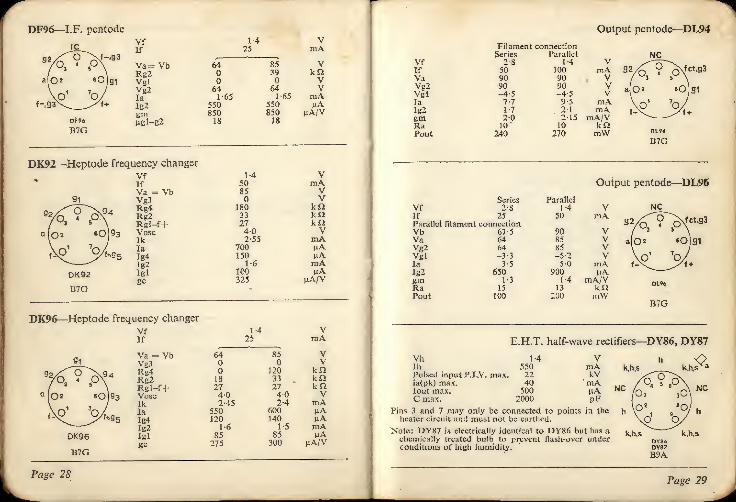
DF96—I.F. pentode
DK92—Heptode frequency changer
14 V25 mA
64 85 V39 kn
V64 64 V
1- 55 1-65 mAS30 550 jiA850 850 |iA/VIS IS
1-4 V50 mA85 V
V180 km33 kn27 kO40 V2-55 mA
700 "A150 jiA
1-6 mA100 uA325 uA/V
DK96—Heptode frequency changer
vfIf
DK96
14 V25 mA
64 85 VV
120 kn18 33 kfl27 27 kn40 40 V2 -45 2-4 mA
550 600 uA120 140 UA
1-6 15 mA85 85 pA275 300 uA/V
B7G
Page 28
Filament connectionSeries Parallel
Vf 2-8 1-4 VIf 50 100 mAVa 90 90 VVg2 90 90 VVgl -4-5 -4-5 Vla 7-7 9-5 mAIg2 1-7 21 mAgm 2-0 2-15 mA/VRa 10' 10 knPout 240 270 mW
Output pentode—DL94
fct,g3
B7G
Series
Vf 2-8
if 25Parallel filament connectionVb 67-5
Va 64Vg2 64Vgl -3-3
la 3-5
Ig2 650gm 1-3
Ra 15Pout 100
Parallel
l<4 V50 mA
90 V85 V85 V-5*2 V5-0 mA
900 mA1-4 mA/V
13 kn200 mW
Output pentode—DL96
fcts3
B7G
E.H.T. half-wave rectifiers—DY86, DY87
Vh 1-4
lh 550Pulsed input P.I..V. max. 22ia(pk) max, 40lout max. 500C max. 2000
Pins 3 and 7 may only be connected to points in theheater circuit and must not be earthed.
Note: DY87 is electrically identical to DYS6 hut has achemically treated bulb to prevent flash-over underconditions of high humidity.
Page 29

EABC8G—Triple diode triode
6-3 V450 mA
100 250 V-1-0 -3-0 V0-8 1-0 mA1-45 1-4 mA/V
70 70
B9A
Page 30
Double diode pentode—EBF80
VhIhVa - VbRg2Vg2Vg3TtklaIg2gmngi-e2
6-3
3002509585
3005-01-752-2
13B9A
6-3 V300 mA
6-3 12-6 25 VV
6-3 12-6 25 V2-2 2-2 2-2 M£20-12 0-45 1-7 mA004 0'14 0-5 mA0-45 10 2-1 mA/V0-65 10 0-2 Mfl
Double diode pentode for use in hybrid car radios—EBF83VhIh
VaVg3Vg2RgllaIg2gmra 0-65 1-0 0-2 MSi
B9A
Double diode variable-mu r.f. pentode—EBF89
VhIh
VaVg3Vg2Vgllamgmra
Pg'-g2B9A
Page 31
6-3 V300 mA
250 250 VV
so 100 V-1-0 -2-0 V90 9 mA2-7 2-7 mA4-5 3-8 mA/V0-9 1-0 Mil20 20

ECC81—R.F. double triode (separate cathodes)
Scries ParallelVh 12-6 63 VJh 150 300Characteristics (each section)Va 200 250 VVg -1-0 -2-0 Vla 11-5 10 m A.gm 6-7 5-5 niA/VJ-i 70 60
ECC82—Double triode (separate cathodes)
SeriesVh 12'6Ih 150Characteristics (each section)Va 100Vg ola 11-8gm 3'1
H 19-5
ECC83—Double triode (separate cathodes)
SeriesVh 12-6
,Ih 150Characteristics (each section)Va 100Vg -1-0
r la 0-5
gm 1 .25
net *10°
Page 32
Parallel6-3 V
300 mA.
250 V-8-5 V10-5 mA.2-2 mA/V17
Parallel6-3 V
300 mA250 V-20 V1-2 mA14 mA/V
100
R.F. double triode (separate cathodes)—ECC84
Ih 330Characteristics each section)
Va 90Ve -I "5
gm o-O
3 24
R.F. double triode (separate cathodes)—ECC85
Vh 6-3
Ih 435Characteristics (each section)
Va 250Vg -2-3
Ia io
gm 5'9
H 57
V.H.F. double triode (separate cathodes)—ECC88
Vh 6-3
Ih 365Characteristics (each section)
Va 90Vg -1-3
la 15
gm 12'5
£ 33
Page 33

ECC804/6/30L2—Double triode (separate cathodes)
ECCB04/6/3OL2
Vh 6-3
lh 300Characteristics (each section)
Va 200Vg -7-7
la 10gm 3-4
p 18
B9A
VniA
VV
niAmA/V
ECF80—-Triode pentode (separate cathodes)
s- 3 V430 mA
Triode Pentode100 250 V
200 V-2-0 3-2 V14 7-0 mA—
,
1-8 mA5 5-5 mA/V
20 — '
B9A
Vh IH Vlh 450 mA
kp.
P Triode Pentodes Va 150 250 V
Vg2 110 Vkt Vgl -to -0-9 V
la 18 10 mAIg2 -
—
3-5 mAgm 8-5 5-2 mA/Vt^ 40 —
Page 34
ECF82—Triode pentode (separate cathodes)
Triode hexode frequency changer—ECH42VhlhVal> = VbVS2 + g4KkRa3 -r St1*3 -: &lah
w- -g4gcVatlat
'
6-3
23025085ISO47
2003-0
30750904'8
B8A
Triode hcptodc frequency changer—ECH81VhlhVah = VbRg2 + g4Rg3 -r gt
RklabIg2 + g4lg3 + gtgcVatlat
6*3
3002502247140
3-256-7
200775100
4-5
Triode heptode for use in hybrid car radios—ECH83VhlhVah = VbVg2 + g4Vgllah.
Jg2 + g4IS + gtVosc(r.m,£.)geraVatlat
Vb
6-3 V300 mA12-6 V12-6 V
V100 nA350 pA32. [iA1:2 V
160 pA/V3-8 Ma12-6 V
750 pA
k,35
B9A
Page 35

ECH84—Triode heptode for noise cancelled sync, separator
B9A
Vh 6-3 VIh 300 mA
Triode HeptodeVa 50 135 VVg3 — VVg2 4- g4 — 14 VVgl Vla 3 1-7 mAIg2 + g4 .
—
900 HAgm 3-7 2:2 mA/Vu 50 —Vg3(Ia = 20uA) — -2 VVgl (la = 20mA) — -i-S VIa(Va = 200V,Vg = -llV) <100 — HA
ECL80—Triode output pentode (pa max. = 3-5W)6-3 V
300 mATriode 1'entodc100 200 V— 200 V— V-2-3 -8-0 V4-0 17-5 mA— 3-3 mA1-4 3-3 mA/V
17-5 —— 11 kn— 1-4 w
ax, = 5-4WJ6-3 V
780 mATriode Pentode100 250 V— 250 V
3-5 28 mA— 5-7 mA-22-5 V
2-5 50 mA/V— 9-0 kfi— 3-4 W
ECL82
Page 36
Triode output pentode (pa max. = 5-4W)—ECL83
vhIh
VaVg2lalg2VglgrnraRaPout
6-3 V600 mA
Triode Pentode200 200 V
200 V2-4 27 mA— 4-4 mA
-1-5 -13 V2-5 5-0 mA/V
34 65 kn— 7-5 kn— 2-5 wB9A
VhIn.
VaVg2laIg2Vglgmra
RaPout
Triode output pentode (pa max, -—- 9W)
—
ECL86
6-3 V700 mA
Triode Pentode250 250 V
i
—
250 V1-2 36 mA
.
—
60 mA-1-9 -7-0 V
1-G 10 mA/V62 48 kn— 70 kn— 40 w
B9A
VhIhVaVg2Vg3RklaIg2gmH£l-£2
6-3
300170170
160102-5
7*450
High slope r.f, pentode
—
EF80
B9A
Page 37

EF83—Variable-mu a.f. voltage amplifying pentode
6-3 V200 mA250 V
V50 V-1-6 V4-0 mA115 mA!<€ mA/V
10
B9A
EF85--Variable-mi r.f. pentode
h Vhh
<""cTs Ih
Vh = -- Va
h
f°
o4 %
7°1a
Ri:2VE 2
Rk\r> 2 •O/ Is
31
kEFB5
03
yz Ig2gm
B9A
6-3 V300 mA250 V60 kfi100 V160 SI
10 mA2-5 mA6-0 mA/V
EF86—Low noise a.f. voltage amplifying pentode
s\0 3
h Vh
9>\a Ih
Va
tOA s Vg3Vg2
( Oy33Vglla
oy Ig2_~>si gmMgl-g2
EFB4
B9A
6-3
200250
140-2-03-0
6002-0
38
VmAVVVV
mAUA
mA/V
Page 38
Variable-mii r.f. pentode—EF89
vhlhVaVg3Vg2RklaIg2gm
6-3
200250
100160
9-03-03-6
High slope r.f. pentode—EF91
VhlhVaVg2Vg3Rkla
Ig2gmMgl-g2
6-3
300250250
160102-67-6
70
VmAVVVn
mAmA
mA/V
UK5 *W k*)
Vhlh
VaVg2Rklalg2gm
V.H.F, pentode—EF95
k,g3,s
Page 39
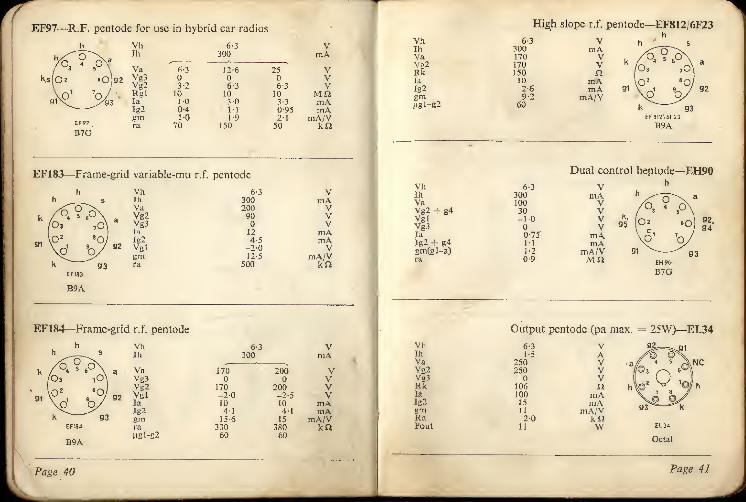
EF97—R.F. pentode for use in hybrid car radios
6-3
300
6-3
3-2
10100-41*0
70
12-6
6-3
103-01-1
1'9
150
25
6-3
103-30-952-1
50
6-3
30020090
124-5
-2-012-5
500
VBlA
VVV
MfimAmA
mA/V
EF183—Frame-grid variabk-mu r.f. pentode
h VmAVVV
mABlAV
mA/Vkfi
VhIhVaVg2Rklalg2gtapgl-g2
High slope r.f. pentode—EF812/6F23h
6-3 V h300 mA o170 V
nUX
170150
V£1
tO\
10 mA \o 2 «oi2-69-2
mAmA/V
31 \o1 V60 k S3
EF812\&F23
B9A
Dual control heptode—EH90Vh 6-3 V h
IhVaVg2 + g4
30010030
mAVV
& b. so) nVgtVg3
-l'O VV
lalg2 + g4
0-75M mA
mA31 ^ " S3gm(gl-a) 1-2 mA/V
ra 0-9 Mfi £H9C
B7G
EF184—Frame-grid r.f. pentode
.
Page 40
H£l-g2
6-3 V300 mA
170 200 VV
170 20 i) V-2-0 -2-5 V10 10 mA41 4-1 mA15-6 15 mA/V
330 380 kfi60 60
Output pentode (pa max. = 25W)
—
EL34
VhIhVaVg2Vg3Rkla
Ig2gmRaPout
6-3 V1-5 A
250 V250 V
V106 n100 mA15 mA11 mA/V2-0 kfi
11 WOctal
Page 41

EL81—Line timebase output pentode (pa max.
-Xa
IhVaVg2Vg3Vg!lamgmHg!-g2
tun
B9A
8W)
6-3 V105 A
250 V250 V
. V-38-5 V32 mA2-4 mA4-6 mA/V5-1
Double output pentode (pa. max. = 2 x 6W)—ELL80Vh 6 "3
Ih 550Characteristics (each section)
Va 250
Vg2 250
*Rk 160
Ia 24
Ig2 4 '5
gm 6 ' 3
Ra 10
Pout 3
'Common to both sections B9A
EL84- -Outp ut pentode (pa max. » 12W)h
VhThVaVg2RkI a
Ig2gmRaPout
B9A
6-3
760250250135485-5
It -3
4-55-7
EL95—-Output pentode (pa max.h
6W)
VhIh
5 \ Va
«0;g2 Vg2VglV la
/01 gmRa
EL95Pout
6-3
200250250-9-0
244-5
58-02-3
VmAVVn
mAmA
mA/Vknw
vmAVVV
mAmA
mA/Vknw
VhIhVbVlRaRg-k
VgBlaIt
6-3 V300 mA250 V250 V500 kn
3 Ma-10 -10-5 V65 5 deg370 20 J-iA
20 2-3 mA
Tuning indicator—EM81h
Voltage indicator—EM84VhIhVbVtRaRg-k
VglaIt
*L
Deflection electrode connected to anode.•Length of column.
6-3 V210 mA250 V250 V470 kn
3 Mn-22 V
450 60 uA10 1-8 mA
21 mmEM34
B9A
Page 42 Page 43

EM87—Voltage indicator
VhIh
6-3
300V
mAVb 250 VVt 250 VRa 100 kS2Rg-k 3 -Mfi
Vg -10 -15 VTa 2 e 0-5 0-2 mAIt 1 1 8 2-0 ,mA*L 21 -l»3 mmDeflection electrode connected to anode.
*Lengtti of column. A negative Yahie of L indicatesoverlapping.
Full-wave rectifier—EZ80
Vh 6-3 VIh . 600 mA.Vin (r.m.s.) 2 X 350 Vlout max, 90 mAC max. 50 HFRlim min. (per anode) 300 fi
EZ80
B9A
EY5I—High voltage half-wave rectifier
6-3
90
17
350so
5000
Wircd-in
EY86, EY87—High voltage half-wave rectifier
vmAkVpAmA
VmAkVu.AmAPF
B9A
Vh 6-3
Hi 90Pulsed inputP.I.V. max. 22lout 800ia(pk) max, 40'
C max. 2000
fPins 1, 4, 6 and 9 may be used for fitting an anti-corona shield.
*PiOB 3 and 7 may only be connected to points in theheater circuit and must not be earthed.
Note: EY87 is electrically identical to EY86 but has achemically treated bulb to prevent flash-over underconditions of high humidity.
Vh 6-3
Ih 1-0
Vin(r.m.S-) 2 X 350lout max. 160C max. 50Rlim ruin, (per anode) 230
VhIhVinCr.m.s.)lout max.C max.
519
2 X'45025060
Rlim min. (per anode) 1 50
Full-wave rectifier—EZ81
V h
A Kef n -\ICV /4 s P\mA k 'O, tOV"uFa !C \°' e O/lC
EZ81
B9A
Full-wave rectifier—GZ34NP
GZ34
Octal
Page 44 Page 45

r KY50/U25—E.H.T. rectifier
/ Ih 200 mAVh 2 V 36cm (!4in> Television tube. Magnetic focusing.
s^*i P.I.V. max. 19 kV 70 J Magnetic deflection. Incorporates ion trap. Ion
/ V ia{pk) max. 25 mA trap magnet IT9./ ) la max. 0-2 mA Final anode cavitv connector tvpc CT8.
<C / Vout 16 kV Vh 6-3 VIh 300 mA
h ^far Va3 12 kVVa2 V
kh KY50/US» Va 1 250 VVg for cut-off -33 to -72 V
Wired-in
MW36-44
B12A
KY80/U26—E.H.T. Rectifier
h,v a
h,k,s Ih 350 mAVh 20 VP.I.V. max. 23-5 kVla max. 0-2 mAia(pk) max. 60 mA
h.k.s
Kvao'uz*
E9A
MW36-24
;
36cm (I4in) Television tube, Magnetic focusing.70" Magnetic deflection. Incorporates ion trap. Iontrap magnet IT9.Final anode cavity connector type CT8.
6-3
30012
250-33 to -72
VmAkVVV
MW36-24
BI2A
Page 46
MW43-69
43cm (17in) Television tube. Magnetic focusing.
IQr Magnetic deflection. Incorporates ion trap. Iontrap magnet IT9. Metal-backed screen.
Final anode cavity connector type CT8.
Vh 6-3
Ih 300Va3 14
Va2Val 300Vg for cut-off -40 to -86
BI2A
43cm (17in) Television tube. Magnetic focusing.90" Magnetic deflection. Incorporates ion trap. Iontrap magnet IT9. Metal-backed screen.
Final anode cavity connector type CT8.
Vh 6-3 Vlh ! 300 mAVa3 14 kVVa2 VVal 300 VVg for cut-off -40 to -86 V
MW43-80IC 02
Page 47
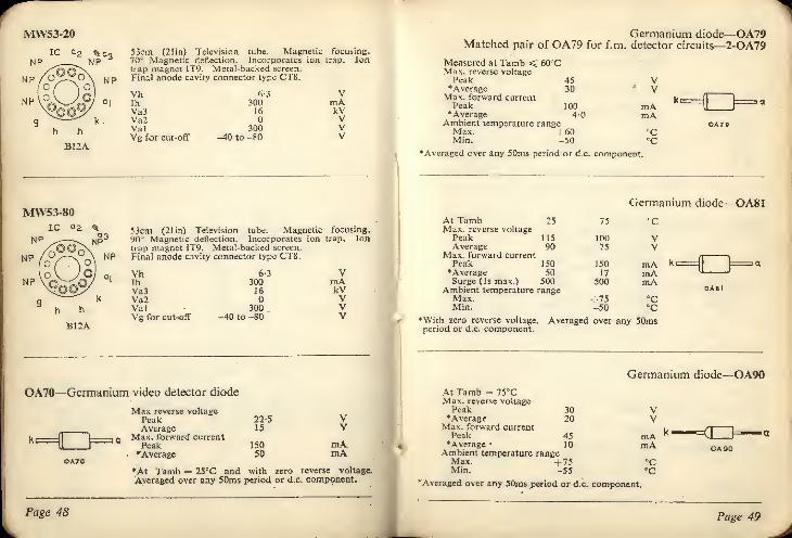
MW53-20
53cm (21 in) Television tube. Magnetic focusing.70° Magnetic deflection. Incorporates ion trap. Iontrap magnet IT9. Metal-backed screen.
Final anode cavity connector type CT8.
VhHiVa3Va2ValVg for cut-off
6-3
30016
300-40 to -80
VmAkVVVV
Germanium diode—OA79Matched pair of OA79 for f.m. detector circuits—2-OA79
Measured at Tamb < 60CMax. reverse voltagePeak 45 V
* Average 30 VMax. forward current
Peak 100 mA'Average 4-0 mA
Ambient temperature an«eMax, - 60 CCMin. -50 •e
*Averaged over any 50ms period or d.c. component.
HLJ='
53cm (21in) Television tube. Magnetic focusing.
90J Magnetic deflection. Incorporates ion trap. Iontrap magnet IT9. Metal-backed screen.
Final anode cavity connector type CT8.
VhInVa3Va2ValVg for cut-off
6-3
30016
300-40 to -80
VmAkVVVV
Germanium diode
—
OA81
At Tamb 25 75 CCMax. reverse voltagePeak 1 1
5
100 VAverage 90 75 V
Max. forward currentPeak 150 150 mA'Average 50 17 mASurge (Is max.) 500 500 mA
Ambient temperature rangeMax. + 75 °cMin. -50 'C
•With zero reverse voltage.period or d.c. component.
Averaged over any 50ms
i - I 1 1
OA70—Germanium video detector diode
=(1 \
=='
Max reverse voltagePeak 22-5 VAverage 15 V
Max. forward currentPeak 150 mA
*Average 50 mA
*At Tamb = 25 °C and with zero reverse voltage.
Averaged over any 50ms period or d.c. component.
At Tamb = 75°CMax. reverse voltagePeak 30*Average 20
Max. forward currentPeak 45'Average 10
Ambient temperature rangeMax. +75Min. -55
Germanium diode
—
OA90
mAmA"C
'Averaged over any 50ms period or d.c. component.
Page 48 Page 49

OA91—Germanium diode
At TambMax. reverse voltagePeakAverage
Max. forward current
Peak'Average
Ambient temperature range, Max.I Min.
'With zero reverse voltage,
period or d.c. component.
11590
150*50
60
10075
15017
mAm A
Averaged over any 50ms
OA2G2—Silicon junction diode
At Tamb 25 125 °C
Max. reverse voltage(peak or d.c.) 150 150 VMax. forward currentPeak 250 J 25 mAD.C. 160 48 mAAverage 88 40 mA
Ambient temperature rangeMax. |
125 "CMin. -55 cc
•Averaged over any 50ms period or d.c. component.
OA210—Silicon junction diode
'-q
At Tamb - 70°CMax, I'.l.V.
Max. forward current'
Peak (atP.I.V. max.)•AverageMax, ambient temperature
•Averaged over any 50ms period or d.c. component.
400
5
50070
AmACC
Silicon zener diode—OAZ210
Page 50
Max, forward currentPeak 250
[•Average 100Max, zener current
Peak 250•Average 40
Surge (max, duration100 us) 10
Zener voltage at zenercurrent ofImA 6-25mA 6-3
20mA 6-4•Ptot max, (without
cooling clip) 310
mAmAmAmA
Coloured
dot
r%fAveraged over any 20ms period or d.c. component
At Tamb - 253C.
KP-N-P power junction transistor—OC16W
etblue)
Vcb max. —16VcEmax. -16•Ic(av) [-5
Icbo(Vcb = -14V) 20Ptot max. (Tease m 75'Q 109j-case 1 '0
Averaged over any 20ms period.
VVAuAW
°C/W
P-N-P power junction transistor—OC19
Measured at Tj = 25'=CVce -7-0 VIc 300 mAf 10 kc/shFEL 45Icbo (Vcb - -14V) <100 pAPtot max. (Tease = 45'C) 24 wOj-case 1 °c/w
Page 51
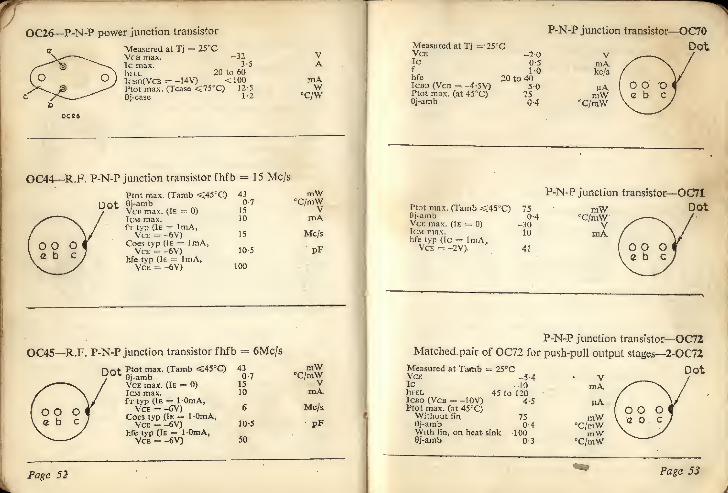
OC26—P-N-P power junction transistor
Measured at Tj = 25°CVca max. -32
Ic max. 3-5
hFEL 20 to 60
JcboCVcb = -UV) <100Ptot max. (Tease <75°C) 125Oj-case 1'2
VA
mAW
X'W
Measured atTj =-25°CVce -2*0Icf
0-51-0
hfe 20 to^ICBO (VCIJ = -4 5V) 50Ptot max. (at 45°C) 75Oj-amb 4
P-N-P junction transistor—OC70
Dot
OC44—R.F. P-N-P junction transistor fhfb = 15 Mc/s
Ptot max. (Tamb <4S°QDot Oj-amb
Vce max. (Ie = 0)
1cm max,f r tvp (Ie = I mA,Vce = -6V)
Coes typ (Ie = 1mA,Vce = -6V)
hfe typ (Ie = 1mA,Vce = -6V)
430-7
15
10
15
105
100
mWcC/mW
VmAMc/s
pF
Ptot max. (Tamb <45 CC) 75Oj-amb 0-4Vce max. (Ie - 0) -30lew max. 10hfe typ (Ec == 1mA,Vol = -2V). 41
P-N-P junction transistor—OC71Dot
OC45—R.F. P-N-P junction transistor fhfb » 6Mc/s
qq^ Ptot max. (Tamb <45°Q 43Oj-amb 0-7
Vce max. (Ie = 0) 15
Icm max. 10
fr typ (Ie = 1'OmA,Vce = -6V) 6
Coes typ (Ie = 1-OmA,Vce --6V) 10-5
hfe typ (Ie = 1-OmA,Vce - -6V) 50
mW°C/mW
VmAMc/s
pF
Page 52
P-N-P junction transistor
—
OC72Matched. pair of OC72 for push-pull output stages—2-OC72
Measured at Tamb = 25"C DotVce -5-4Ic _ioIiiel 45 to 120Icuo (Vcb as -10V) 4-5Ptot max. (at 45
;
'CjWithout fin 75Oj-amb 4With fin, on heat sink 100Oj-amb 0-3
^ Page 53

OC74—P-N-P junction transistor
2-OC74—Matched pair of OC74 for push-pull output stages
DotMeasured at Tamb = 25'
C
Vce -6-0 VIc 50 mAh« 100Icbo (VCB - -9V) 10 pAPtot max. (Tamb = 45*Q 135 mWOj-amb (in free air) <0-22 °C/mW
OC75—P-N-P junction transistor
Dot Measured at Tamb -
VceIchfeIcbo(Vcb = -4-5V)Ptot <Tamb = 45 C)Oj-amb
-2-030
904-5
75<0-4
OC78—P-N-P junction transistor
Dot Measured at Tj = 2 5CC
Vce -TOIc 125
hFEL >25ICBO(VCB = -10V) <10Oj-amb {free air) 0-25
Oj-amb (with fin, on heatsink) 015
Page 54
vmA
UAmW
cC/mW
VmAHA
°C/mW
°C/mW
P-N-P junction output transistor
Ptot max. (Tamb <45*Q 200 mW0j-amb 0-2 'C/mWVce max. (Ik - 0,
Rbe <Ik£2) -20 VTcm max. 500 mAhfe min. (Ic = 300mA) 45
P-N-P junction driver transistor—OC81DDot.
Ptot max. (Tamb =£45O I0& mW6j-amb 0-4 °C/mWVce max. (Ie = 0,
Rbe <2kO) -20 V1cm max. 50 mAhfe tvp (rE 10mA,Vce - -6V) 60
P-N-P junction transistor
Measured at Tj = 25r
'CVce -1-0 VIc 250 mAhFEL >45Icbo(Vcb = -10V) <10 ,u.A8j-amb (free air) 0-2 "C/mWOj-amb (with a clip, on.
a heat sink) CM "C/mW OC82
Page 55

OCI70—R.F. P-N-P alloy difFased junction transistor fl = 75
Mc/s
intcrload shield
and metal caseMeasured at Tamb = 25"CVce1ef
hfc
Jcno (Vcb « -6-QV)Ptot mas. (Tamb = 45 °C)Oj-ambPower gain (f — 10 Mc/s)
-6-0 V1-0 mA1-0 kc/s
1501-2 uA
50 mW=£0-6 °C/mW25 <1B
OC171—R.F. P-N-P alloy diffused junction transistor fl = 75
Mc/s
intcrlead shield
and mctaf case
/e br cs
Measured ; it Tamb = 2 5rC
Vce -6-0
IE 1-0
f 10hfc 150Ia so (Vcb = -6'0V) 1-2
Ptot max. (Tamb = 45GC) 50
Oj-amb sSO-6
Power gain (f = 100 Mc/s) 14
VmAkc/s
uAmW
°C/mWdB
ORP12—Cadmium sulphide photoconductive cell
Direction of. lightCell resistance
Tight resistance at 1000 lux
(93 Im/fl 2) and lamp colour
temperature of 2700 :K 75 to 300
Bark resistance 5*10
V cell (d.c. or pk.) max. 110
p cell max. at Tamb<40 ;C 200- 50
:C 100
TambMaximum -H 60
Minimum -"10
aMfiV
mWmW°CT
Page 56
Cadmium sulphide photoconductive cell—ORP60Cell current at 30V d.c, 54
(5-0 lm/ft 2) and lamp co'.
temperature 270O"KMinimumAverageMaximum
Max. ultimate dark currenat 300V d.c.
V cell (d.c. or pk) max.p cell max. at Tamb.<25=C= wc
I cell max.TambMaximumMinimum
lux.our
200500800t
1-5
350
70207-5
i-70^10
uAHAUA
uAV
mWmWmA
°C
Direction of light
If
Triple diode triodc (one diode having a separate cathode)—PABC80ihVh
VaVglaem
300 mA9-5 V
170 200 V-1-85 -2-3 V10 10 mA1-45 1-4 mA/V
48 50 kfl70 70
k'W03 7 o^
kt.kil,
\ k'"d,s
a'i?2
,
a'"dV.3/9
PABC80
B9A
IhVhVaVglagin
U.H.F. Frame-grid mixer/oscillator triode—PC86h
3003-8
175
-i-512144-85
mA x£TO~>vV k
/o* V ,o\V /Os 7V
mA \o 2 *omA/V
k£2i.
1
a a
PC 86
B9A
Page 57

PC88—U.H.F. Frame-grid grounded grid amplifier triode
PC900—R.F. triode
IhVhVaVglagmk 0* «0 s
W To/ ra9^^^PC TOO
B7G
Page 58
3003-8
160-1-2512 5
13-54-8
65
30040
135-1-0n-514-5
725-0
mAVVV
raAmA/V
kfl
300 rhA4-5 V
135 V-10 Vli mA13 mA/V6550 kfl
mAVVV
mAmA/V
kSl
Ih 300Vh 7-0Characteristics (each section!Va 90Vf -1-5la |2gm 6-0u. 24
Double triode (separate cathodes)—PCC84hmA
V
VV
mAmA/V
Ih 300Vh 9-0Characteristics {each section)
VaVgfagmU
Double triode (separate cathodes)—PCC85
hmAV
170-V510S-2
50
200 V-2-1 V1 1) m 45-8 mA/V
4S
B9A
lh 300Vh 7-0Characteristics (each section)Va 90Vg -13la 15gm 12-5
M 33
Frame-grid double triode—PCC88h
Page 59

PCC89—Variablc-mu frame-grid double triode.
h ih' 300
Vh '.
,'"5
Characteristics (each section)
r 36
mAV
VmAV
mA/V
PCC189—V.H.F. Variable-mu frame-grid cascode double triode
hIh 3°°
Vh 7-6
Characteristics (each section)
mAV
Vg (for 20:1reduction in gm)
Vg (for 100:1
reduction, in gm)
90-1-41512-52-5
34
-50
-9-0
VV
mAmA/V
kil
!d
L
PCC805/30L15—R.F. cascode double triode
h g i h 300
x Vh ,7-0
Mt i tu \ v' Characteristics (each section)
Va 90
k" a1
FCC805\3OLtS
B9A
Page 60
mAV
VV
mAmA/V
IhVh
VaVg2lagmu
IhVh
VaVg2VgllaIg2gmV-
IhVh
VaVg2VgllaIg2gm
Triode beam tetrode—PCE800/30FL1300 mA
9-4 V
Triode Tetrode200 170 V— 170 V10 10 mA3-4 8 mA/V18 —
PCE80O/30FL1
B9A
Triode pentode (separate cathodes)—PCF80300 mA
9 V
Triode Pentode100 170 V— 170 V-2-0 -2-0 V14 10 mA— 2-3 mA5
206-2 mA/V
Triode pentode (separate cathodes)—FCF82
h
Page 61

PCF84—Triode pentode
k.g3.s
ThVh
VaVg2Vglla1*2gm
B9A
100 mA9-0 V
Triode Pentode100 170 V
. 170 V-20 -2-0 V14 12 mA
3 mA5-0 7-5 mA/V40 400 kn
PCF86--Triode frame-grid pentode
3008
Triode100
-314
5-7
3
Pentode170150-1-2103-3
12>350
mAV
VVV
mAmA
mA/V
B9A
PCF800/30C15—V.H.F. Triode pentode
30090
k,g3,s
Page 62
Triode100
IS6-0
20
Pentode170170109-0
mAV
VV
mAmA/V
.
lhVh
VaVg2VgllaIg2gmHra
lhVh
VaVg2VgllaIg2gmMra
lhVh
VaVg2VgllaIg2gmVl'gl-g2
Triode frame-grid variable-mu pentode—PCF801
Triode pentode—PCF802300 mA9 V
Triode Pentode200 100 V—
.
100 V-2-0 -1-0 V3-5 6-0 mA— M mA3-5 5-5 mA/V70 —20 400 kn
B9A
V.H.F. Triode pentode—PCF805/30C18
K,S3,S
PCF80j;30C18
B9A(Shield completelysurrounds pentode)
Page 63

PCF806—Triode frame-grid pentode
3008-0
mAV
Triode Pentode100 170 V
150 V-3 -1-2 V14 10' mA
.
—
3-3 mA5-5 12 mA/V
17 —
PCL82—Triode output pentode (pa max. = 7W)
300 mA16 V
Triode Pentode100 170 V
no V-11-5 V
3-5 41 mA. 90 mA2-2 7-5 mA/V70 —
i
— 3-9 kn— 3-3 wB9A
300 mA12-6 V
Triode Pentode250 170 V
. . 170 V-8-5 -9-5 V10-5 30 mA
5 mA2-2 5-5 mA/V17 —
5*S kn— 2-2 w
Page 64
Triode output pentode (pa max PCL84
PCL83—Triode output pentode (pa max. = 5-4WJ
i!i
VIi
VaVg2VailaIg2
ugl-g2
WO mA15 V
Ti i d
c
Pentode200 21)0 V
, 200 V-1-7 -2-9 V3-0 18 mA
,
—
3 mA40 10-4 mA/V
16-2 130 kQ— 36
1
Triode output pentode (pa max PCL8S
iti
Vh
VaVg2VglI a
Ig2gmra
Hgl-§2
300 IKA18 V
Triode Pentode100 170 V„ .170 V
-15 V10 41 mA
27 mA5-5 7-25 mA IV
9 25 kQ— 7-0
Triode output pentode (pa max. (pentode)
IhVh
VaVg2Vglla
Ig2gmraHgl-g2
300 mA13-3 V
rriode Pentode230 230 V
i
—
230 V-1-7 -5-7 V1-2 39 mA
,
—
6-5 mA1-6 10-5 mA/V
45 kn— 21
9WJ—PCL86h
Page 65

PCL88/30PL14—Triode output beam tetrode
ft
h
"O5 * \
70\32
IhVh
Vakq\0 S
9tV
s oJkt
>atVg2lagm
PCL8B/30PLI4
B9A
300 mA16 V
Triodf Tetrode100 170 V—
,
170 V10 50 mA4-3 7-3 mA/V18 _^
IhVhVaVg3Vg2VgllaIg2Rkgm
H.F. screened pentode (pa max. 3W)—PF8I8/30F5300
7'3
170
170-1-9102-6
1508-8
PCL800/30PL13—Triode output beam tetrodeh
ft s P-CIM/Oi tO\92
kq,\0 2
bP 'S\01
•O/kl
>2PCL800/30PL13
B9A
IhVh
VaVg2laIg2gnili
300 mA16 V
Triode Tetrode100 170 V
170 Vto 45 mA.— 8-7 mA,4-3 7-5 mA/V18 —
PCL801/30PL1—Triode beam tetrode (AF or field output)
300 mA13 V
Triode Tetrode200 170 V— 180 V10 32 mA3-4 7 -2 mA/VIS —
Double pentode (pa max. (output section) = 5W)—PFL200
Page 66
ihVh
VaVg2VgllaIg2gmPgl-g2
300 mA16-5 V
Amplifier Outputsection section150 170 V150 170 V-2-3 -2-6 V10 30 mA30 6-5 mA8-5 21 mA/V35 32
160 40 knB10B
Line timebase output pentode (pa max. = 12W)
IhVhVaVg2Vgllalg2gmugl-g2
30025100100-8-210070145 6
Pace 67
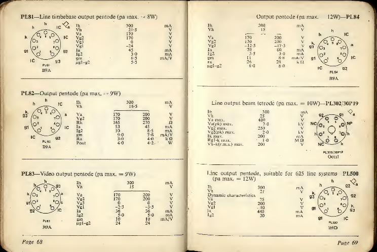
PL81—Line timbebase output pentode (pa max. = 8W)
300 mA21-5 V170 V170 V
V-24 V45 mA.3-0 mA6-5 mA/V5-5
PL82—Output pentode (pa max. = 9W)
300 mA16-5 V
170 200 V170 200 V165 270 n53 45 mA10 8-5 mA9 7-6 mA/V3-0 4-0 kfi40 4-2 W
B9A
PL83—Video output pentode (pa max. = 9W)
IhVh
VaVg2Vg3VgllaIg2
Pin Sm_
„„, ^El-S2B9A
300 mA15 V
170 200 V170 200 V
V-2-3 -3-5 V36 36 mA5-0 5-0 mA10 10 mA/V24 24
Page 68
Output pentode (pa max. = I2W)—PL84
ihVh
VaVg2VgllaIg2gmraMg I-g2
300 mA13 V
170 200 V170 200 V-12-5 -17-3 V70 60 mA3-3 3-0 mA
11 B-8 mA/V26 28 kii80 8-0
Line output beam tetrode (pa max. = I0W)-
Jh 300Vh 25Va max. 400V;i(pk) max. 7Vg2 max. 250Vg2(pk) max. 2-0Ik max. 200Rgl-k max. 10Vh-k(r.m.s.) mux. 200
PL302/30P19
Line output pentode, suitable for 625 line systems—PL500(pa max. = 12WJ
Ih 300Vh 27Dynamic characteristicsVa 75Vg2 200Vgt -10la 440tg2 20
Page 69

rPL8D1/30PJ2—-Beam tetrode (A,F. or field output, pa max,
h
k,bp
6W)
300 mA12-6 V
170 V)KQ V-!©-3 V31 mA7-3 tnA5 kQ2'25 W
IhVhP.I.V. max.Ia(av) max,C max.vh-k(pk) max.
(cathode positive)
300174-75
15040
4'75
Booster diode—PY81
PL820—Line timebase output pentode (pa max. — 8W)
B9A
LPage 70
300 mA21 5 V
170 200 V170 200 V
V-22 -28 V45 40 mA3-0 2-R mA6-2 6-0 mA/V5-5 5 5
PY33—Ha If-wave rectifier
a
NP a
/ * 5 \ NP
IhVhP.I.V. max.
30029
700
mAVV
(o 3 ^ p\[O
2 V iQj
Vin(r.m.s.) 200 V
h h
lout max.C max.Rlim min.
32520015
mA
n
NP KPY33
Octal
•
III
VhP.I.V.Vin(r.m.s.) max,lout max.C max.Rlim min.
Ill
VhP.I.V, max.Ia(av) max.vh-k(pk) max.(cathode positive)
30019
700250ISO6045
300306-6
220
6-6
Half-wave rectifier—PY82
PYB2
B9A
mAVkVmA jc
kV
Booster diode—PY88
h O
Page 71
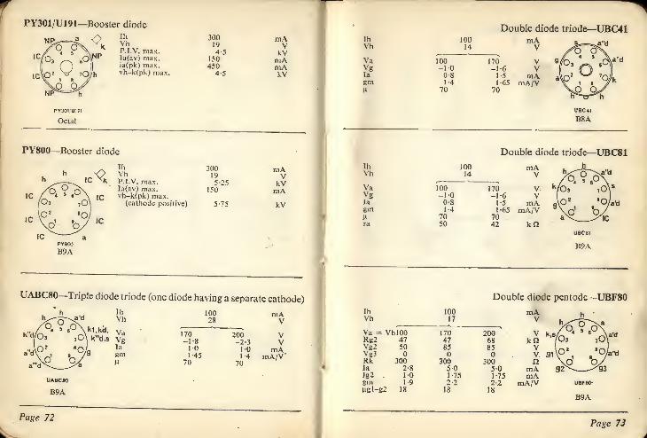
PY301/U191—Booster diode
IhVhP.I.V. max,la(av) max.ia(pk) max.vh-k(pk) max.
PY30i/Ut?l
Octal
PY800—Booster diode
VhP.I.V. max.Ia(av) max.vh-k(pk) max.
(cathode positive)
300194-5
150450
4-5
300195-25
150
5-75
niAVkVmAmAkV
mAVkVmA
kV
UABC80—Triple diode triode (one diode having a separate cathode)
h
,«y * s 6U \kt.kd,
k dfo 3 7o\ k'"d,s
Ih
Vh
VaVr
.. In 1 'cv
\p 0/lagmM
UABC80
B9A
100 mA28 V
370 200 V-1-8 -2-3 V1-0 10 mA145 1-4 raA/V
70 70
Page 72
Double diode triode—UBC41Jh 100 mAVh 14 V
Va 100 370 VVg -10 -1-6 Vla 0-8 1-5 mAgm 1-4 65 mA/VV. 70 70
B8A
Double diode triode—UBC81Ih 100 hVh 14 V
V-
7q t ,o\Va 100 170 k/Oj tO\s
Vg -10 -16 Vla 08 15 mA
3fe &gm 1'4 1-65 mA/VM 70 70 •x>^« ,s*tra 50 42 kfl
uecai
B9A
Double diode pentode—UBF80
Ih 100 mAVh 17 V
Va = VblOO 170 200 VKr2 47 47 68 kiiVr2 50 85 85 Vv«a VRk 300 300 300 £1Ja 2-8 5 5-0 mAIg2 10 1-75 1-75 mAgm 1-9 2-2 2-2 mA/VUgl-i 2 18 18 18
B9A
Page 73

UBF89—Double diode r.f. pentode
ugl-g2
UCC84—Double triode (separate cathodes)
Ih 100Vh 21
Characteristics (each section)
Va 90Vg -1-5
gm o m
v 24
100 mA19 V
100 200 VV
too 100 V-2 -1-5 V8-5 11 itiA
2-8 3-3 mA3-5 4'5 m,4/V
300 600 kii20
UCC85—Double triode (separate cathodes)
mAV
VV
mAmA/V
Ih 100 mAVh 26 V
Characteristics (each section)
Ya 170 200 VVg -1-5 -2-1 Vla 10 10 mAgm 6-2 5-8 mA/Vg 50 48
B9A
Page 74
Ihvh
VaVg2VgJlaTg2gmP
Triode pentode (separate cathodes)—UCF80h
"O
100 mA27 V
Triode Pen kx!e100 170 V— 170 V-2-0 -2 V14 10 mA— 2-8 mA50 6-2 mA/V20
—
Triode hexode frequency changer—UCH42Ih 100 mAVh 14 V
Vah = Vb 100 no 200 VRk 180 180 180 nRftS-fgt 47 47 47 knIg3+gt 100 200 200 jiAVg2-ig4 43 70 85 Vlag 1-2 21 3 mAIg2-fg4 1-5 2-6 30 mAgc 530 670 750 jiA/VVat 70 HI 85 VIat 31 5-7 S*2 mA B8A
Triode heptode frequency changer—UCH81Ih 100 mAVh 19 V
Vah^Vb 170 200 VRg2-!-g4 )0 10 knRg3
:gt 47 47 kn
Rk 150 150 QVg2-i g4 102 119 VIah 3-2 3-7 mAIg2rg4 6-8 8-1 mAIg3+gt 200 230 VtAgc 750 775 pA/VVat 102 120 VIat 4-5 5-4 mA
s fv
B9A
Page 75

UCL82—Triode output pentode (pa max. = 7W)
B9A
Ih 100 mAVh 50 V
Triode PentodeVa 100 200 VVg2 — 200 Vla 3-5 35 mAIg2 70 mAVgl -16 Vgm 2-5 6-4 mA/VRa 5 6 kfiPout — 3 5 W
UCL83—Triode output pentode (pa max. = 5-4W)
ioo38
Triode170
-1-516
2-
82
Pentode170170-9-53055-5
5-52-2
rnAV
VvV
mAmA
mA/V
k(lW
B9A
UF41—Variable-mu r.f. pentode
k,gj
ihVh
Va=VbRg2RklaIg2gmHgl-g2
10012-6
10039330
3-31-01-9
18
17039330
6-01-752-2
18
20039330
7'22-1
2-3
18
mAV
VknQ
mAmA
mA/V
Page 76
IhVh
VaVg3
laIg2gm
High slope r.f. pentode—UF8GIh 100Vh 19Va 170Vg2 170Rk 160la 10Ig2 2-5gm 7-4Hgl-g2 50
Variable-mu r.f. pentode—UF89
100 mA12-6 V
170 200 VV
15 24 kn130 130 a11 11-1 mA3-9 3 8 mA3-8 3-85 mA/V
B9A
Output pentode (pa max. = 9W)—UL41Ih 100 mAVh 45 V
Va 100 170 200 VVr2 100 170 200 VRk 165 165 270 nla 29 53 45 mAm 5-5 10 8-5 mAgm 8 9-5 8-2 mA/VRa 3 3 4-3 knPout 1-35 4-2 4-2 w
k,g3
B8A
Page 77

wUL84—Output pentode (pa max. = 12W)
10045
170 200170 •
170 27070 605-0 4-1
10 8-82-4 2-45-6 5-2
B9A+Vg2(b) = 200V, Rg2 = 470 12
raAV
VVa
mAmA
mA/Vknw
Half-wave rectifier—UY85Ih tooVfa 38Vin(r.m.s.) 250lout max. 110Cmax. 100Ttlim min, 100
UY95
B9A
UM80—Tuning indicator
B9A
UY41—Half-wave rectifier
10019
200200500
3-0
-1045-7
350
-14507010
mAVVV
tnMfi
VdegmAHA
mAVV
mAuFn
Page

rrMINIATURE ELECTROLYTIC CAPACITORS
TOLERANCES WORKINGTEMPERATURES
LEAKAGE CURRENT
-JO to 4-100%for Minimum: -40'
C
After 5 minutes operation at
can size IN 20X: Il<80 x lO^CV-10 to +50% for Maximum con- After prolonged operation at
can sizes tinuous: 20CC: 11<16 x I03CV2N-6N Size IN 60°C
1 Other sizes 70CC After continuous operation at
max. temp.: Ils£80x lO^CVwhere: 11 is leakage current in
microampsC is capacitance in
farads, V is max, voltage in
volts
DIMENSIONS
Can size
BODYLeads (mm)
Length (mm) Dia. (mm)
IN 10-5 3-4 0-6 (23 s.w.g. approx.) x 34
2N 10-5 4-8 0-6 (23 s.w.g, approx.) X 34 '
3N 10-5 61 0-6 (23 s.w.g. approx.) X 34
4N 18-5 6-7 0-8 (21 s.w.g. approx.) X 34
5N 18-5 8-3 0-8 (21 s.w.g. approx.) X 34
6N 18-5 104 0-8 (21 s.w.g. approx.) x 34
Page 80
MINIATURE ELECTROLYTIC CAPACITORS (Cont.)
Capacitance(UF)
M ax.
Voltage(V)
Type No.Insulated
Cansize
1008-0
6 44-02-51-6
100-64
2-5
406410016025-040640
C426AS/A10C426AS/B8C426AS/C6-4C426AS/D4C426AS/E2-5C426AS/F1-6C426AS/G1C426AS/HO-64
IN
40320251601006-4
402-5
2-5
.406-4
1001602540-064
C426AR/A40C426AR/B32C426AR/C25C426AR/D16C426AR/EI0C426AR/F6-4C426AR/G4C426AR/H2-5
2N
8C-064050032-0
2012-5
85
2-54-06-4
10016-0254064
C426AR/A80C426AR/B64C426AR/C50C426AR/D32C426AR/E20C426AR/F12-5C426AR/G8C426AR/H5
3N
160-0125-0100 -0
6404025-0160100
2-54-06-4
10016025-040-0640
C426AR/A160C426AR/B125C426AR/C10OC426AR/D64C426AR/E40C426AR/F25C426AR/G16C426AR/H10
4N
320250-02000125-0800503220-0
2-5
406-4
10016-02540-0640
C426AR/A320C426AR/B250C426AR/C200C426AR/D125C426AR/E80C426AR/F50C426AR/G32C426AR/H20
5N
Page 81

MINIATURE ELECTROLYTIC CAPACITORS (Cont.)
Max.Capacitance voltage Type No, Can
(MF) (V) Insulated size
5000 2-5 C426AR/A5004000 40 C426AR/B400320-0 6-4 C426AR/C320200 100 C426AR/D200 6NJ 25-0 160 C426AR/E125800 25 C426AR/F8050 40 C426AR/G5032 640 C426AR/H32
For details of C426AN and C426AM ranges refer to
previous data book.
Page 82
POLYESTER CAPACITORS
Unless otherwise slated these characteristics refer to 20CC ± 5°,
750 ± 50mm Hg and 60 ± 15% relative humidity,
CAPACITANCE TOLERANCE: ± 10%.MAXIMUM WORKING VOLTAGE: (at temperature up to 85°C>
160V d.c. or 90V r.m.s (f<l kc's) for C296AA series
400V d.c. or 200V r.m.s (f^;500 c/s) for C296AC series
TEST VOLTAGE: 480V d.c. for 125V range for 1 second.1,200V d.c, for 400V range for 1 second,
INSULATION RESISTANCE:(a) at 20^ Capacitance values <0-33 uF I.R.> 50kMfl
Capacitance values > 33 uF RC product 16-5kMfi.uF
(b) at 85X Capacitance values <0-33 uF T.R. > 2-OkMHCapacitance values > 0-33 pp RC product 600 Mil,
uFPOWER FACTOR: <60 X I0"4 at 1 kc/s.
TEMPERATURE RANGE: -40 to + 100=C. For temperaturesbetween 80 and 100"C max., the working voltage should bederated by 0-9%/ t
C.
160V Range
Capacitance Type NumberDimensions in mm
Max.diameter
Max. bodylength
Connectingwire dia.
0-01 C296AA/AI0K 7
21 0-7
(22 s.w.g.
approx.)
0015 C296AA/A15K 7
0-022 C296AA/A22K 7
0-033 C296AA/A33K 7-5
0-047 C296AA/A47K 8
068 C296AA/A68K 9
0-1 C296AA/AI00K 10-5 0-8
(21 s.w.g.
approx.)015 C296AA/A15QK n.
/ 15*17 FLEET ST.,1
REMBEJ&ADIO &
Page 83

POLYESTER CAPACITORS (Com.)
160V Range
Capacitance
amType Number
Dimensions in mmMax,
diameterMax, body
lengthConnectingwire dia.
0-22 C296AA/A220K| 10
35 0-8
(21 s.w.g.
approx.)
0-33 C296AA/A330K[ 12
0-47 C296AA/A470K 14
0-68 C296AA/A680K 16
1-0 C296AA/A1M 18-5
400V Range
Capacitance(MF)
Type NumberDim :n si oils in mm
Max,diameter
Max. bodylength
Connectingwire dia.
0-001 C296AC/AIK 8
21
7
00015 C296AC/AIK5 9
0-0022 C296AC/A2K2 8
0-0033 C296AC/A3K3 8
00047 C296AC/A4K7 8-5
0-0068 C296AC/A6K8 7-5 (22 s.w.g.approx.)
O-01 C296AC/A10K 7-5
0-015 C296AC/A15K 7-5
0-022 C296AC/A22K 8-5
0-033 C296AC/A33K 10 0-8(21 s.w.g.
approx.)0-047 C296AC/A47K 11-5
POLYESTER CAPACITORS (Cont.)
^1
400V Range
Capacitance(MF)
Type NumberDimensions in mm
Max.diameter
Max. body Connectinglength wire dia.
068 C296AC/A68K 9-5
08
01 C296AC/A100K 11
015 C296AC/A150K 12-5
022 C296AC/A220K 14 5 35 (21 s.w.g.
0-33 C296AC/A330K 17approx,)
0-47 C296AC/A470K 195
MINIATURE FOIL CAPACITORS
CAPACITANCE TOLERANCE: ±20%WORKING VOLTAGE: 40V d.e.TEST VOLTAGE (for Is max.): 90V d.c.INSULATION RESISTANCE at 20°C: lOkMfiPOWER FACTOR: s£0-015.TEMPERATURE RANGE: -40 to +8S°C
Capac-itance
0»F)
Type No. Colour Code Max. bodydimensions (mm)
1, h. b.
1st 2nd 3rd 4th
001 C28OAA/PI0K Brown Black Orange Black 12 10 4-0
0022 C2S0AA/P22K Red Red Orange Black 12 10 4-0
047 C280AA/P47K Yellow Violet Orange Black 12 10 4001 C280AA/PI00K Brown Black Yellow Black 12 12 6-0
Page 84 Page $5

VOLTAGE DEPENDENT RESISTORSV.D.R, have a resistance value which varies with theapplied voltage and have been designed for applications in
t.v, receivers and other electronic and electrical equipment
ROD-TYPEMAXIMUM DISSIPATION (Tamb = 40°C): '800 mWTypical Application
:
E298ED/A258 : Damping the primary of frame out-put transformers to prevent ringing and flashover.E29SZZ/06: Rectification of asymmetric pulses (e.g.
to provide a negative voltage for a.g.c. purposes.)The connecting wires are of tinned copper and have adiameter of 0-8mm (21 s.w.g. approx.) and an approxi-mate length of 28mm.
Type No.
E298ED/A256
E298ZZ/06
ReferenceVoltage for
a current of
(V) (mA)
470
950
10
20
D'medians(mm)
Max.; Max.dia. body
length
4-5
4-5
20
20
ColourDot
blackblue
DISC-TYPEMAXIMUM DISSIPATION (Tamb = 40°C): 500 mW
(E299CD/A344: 800 mW)The connecting wires are of tinned copper and have adiameter of 0-Smm (21 s.w.g. approx.) and a length of50mm ._ E299CD/A344 type has solder tags.
Type No.
E299DC/P338
E299DC/P342
E299CD/A344
E299DC/P346
Referencej
Voltage <
for current •
of 1mA Max(V) dia.
Dimensions(mm)
68
100
120
150
Max.thickness
Colour Coding
5-5
6
6-0
70
orange, orange,grey
orange, yellow,.red
orange, yellow,yellow
orange, yellow,blue
Page 86
3
5
s*8
IP
u a
IIm
^8 S
8 8 8IN n wi
SO
8 8
?,s £.c fj3 £j3 3u u U U * m
3 s 3 i § a s 3 S g
oj; o£ ejs n*; g »
u C »> 'C B 'C s S !> uS If 11 i'i 1 §i§
i a i iiijpee »o ono »o c u
3m 3 — 3S 3m,u.SW VX tfl M H
o io w r~— —i M oi
< < < < <> > > > >
Page 87
A

RADIO &TELEvJsi01^
KAYS ELECTRIC
/ 15-17 FLEET ST*
/ PEMBERTON.21ADIO & TELEVISION'3&L: WIGAN 82969,
Mullard Ltd.Milliard House, Torrington Place, London, W.C. 1
.
Printed in England 3539/C88/45M/86S
1
>'

Milliard
<J. .**