€¦ · the oscillator circuit in correct phase and magnitude. therefore, un damped electrical...
TRANSCRIPT
Unit-IV
Oscillators: Oscillator principle, condition for oscillations, types of oscillators, RC-phase shift
and Wein bridge oscillators with BJT and FET and their analysis, Generalized analysis of LC
Oscillators, Hartley and Colpitt’s oscillators with BJT and FET and their analysis, Frequency and
amplitude stability of oscillators.
Oscillators
An electronic circuit used to generate the output signal with constant amplitude and
constant desired frequency is called as an oscillator. It is also called as a waveform generator
which incorporates both active and passive elements. The primary function of an oscillator is to
convert DC power into a periodic signal or AC signal at a very high frequency. An oscillator
does not require any external input signal to produce sinusoidal or other repetitive waveforms of
desired magnitude and frequency at the output and even without use of any mechanical moving
parts.
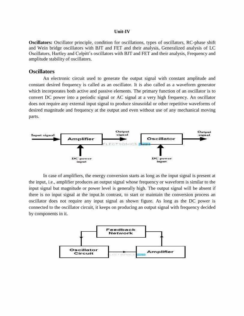
In case of amplifiers, the energy conversion starts as long as the input signal is present at
the input, i.e., amplifier produces an output signal whose frequency or waveform is similar to the
input signal but magnitude or power level is generally high. The output signal will be absent if
there is no input signal at the input.In contrast, to start or maintain the conversion process an
oscillator does not require any input signal as shown figure. As long as the DC power is
connected to the oscillator circuit, it keeps on producing an output signal with frequency decided
by components in it.
www.JntukMaterials.com

The above figure shows the block diagram of an oscillator. An oscillator circuit uses a
vacuum tube or a transistor to generate an AC output. The output oscillations are produced by
the tank circuit components either as R and C or L and C. For continuously generating output
without the requirement of any input from preceding stage, a feedback circuit is used.
From the above block diagram, oscillator circuit produces oscillations that are further
amplified by the amplifier. A feedback network gets a portion of the amplifier output and feeds it
the oscillator circuit in correct phase and magnitude. Therefore, un damped electrical oscillations
are produced , by continuously supplying losses that occur in the tank circuit.
Oscillators Theory
The main statement of the oscillator is that the oscillation is achieved through positive
feedback which generates the output signal without input signal. Also, the voltage gain of the
amplifier increases with the increase in the amount of positive feedback. In order to understand
this concept, let us consider a non-inverting amplifier with a voltage gain ‘A’ and a positive
feedback network with feedback gain of β as shown in figure.
Let us assume that a sinusoidal input signal Vs is applied at the input. Since the amplifier
is non-inverting, the output signal Vo is in phase with Vs. A feedback network feeds the part of
Vo to the input and the amount Vo fed back depends on the feedback network gain β. No phase
shift is introduced by this feedback network and hence the feedback voltage or signal Vf is in
phase with Vs. A feedback is said to be positive when the phase of the feedback signal is same as
www.JntukMaterials.com

that of the input signal. The open loop gain ‘A’ of the amplifier is the ratio of output voltage to
the input voltage, i.e.,
A = Vo/Vi
By considering the effect of feedback, the ratio of net output voltage Vo and input supply Vs
called as a closed loop gain Af (gain with feedback).
Af = Vo/Vs
Since the feedback is positive, the input to the amplifier is generated by adding Vf to the Vs,
Vi = Vs + Vf
Depends on the feedback gain β, the value of the feedback voltage is varied, i.e.,
Vf = β Vo
Substituting in the above equation,
Vi = Vs + β Vo
Vs = Vi – β Vo
Then the gain becomes
Af = Vo/ (Vi – β Vo)
By dividing both numerator and denominator by Vi, we get
Af = (Vo / Vi)/ (1 – β) (Vo / Vi)
Af = A/ (1- A β) since A = Vo/Vi
Where Aβ is the loop gain and if Aβ = 1, then Af becomes infinity. From the above expression, it
is clear that even without external input (Vs = 0), the circuit can generate the output just by
feeding a part of the output as its own input. And also closed loop gain increases with increase in
amount of positive feedback gain. The oscillation rate or frequency depends on amplifier or
feedback network or both.
Barkhausen Criterion or Conditions for Oscillation
The circuit will oscillate when two conditions, called as Barkhausen’s criteria are met.
These two conditions are
1. The loop gain must be unity or greater
2. The feedback signal feeding back at the input must be phase shifted by 360 degrees
(which is same as zero degrees). In most of the circuits, an inverting amplifier is used to
produce 180 degrees phase shift and additional 180 degrees phase shift is provided by the
feedback network. At only one particular frequency, a tuned inductor-capacitor (LC
circuit) circuit provides this 180 degrees phase shift.
Let us know how these conditions can be achieved.
www.JntukMaterials.com
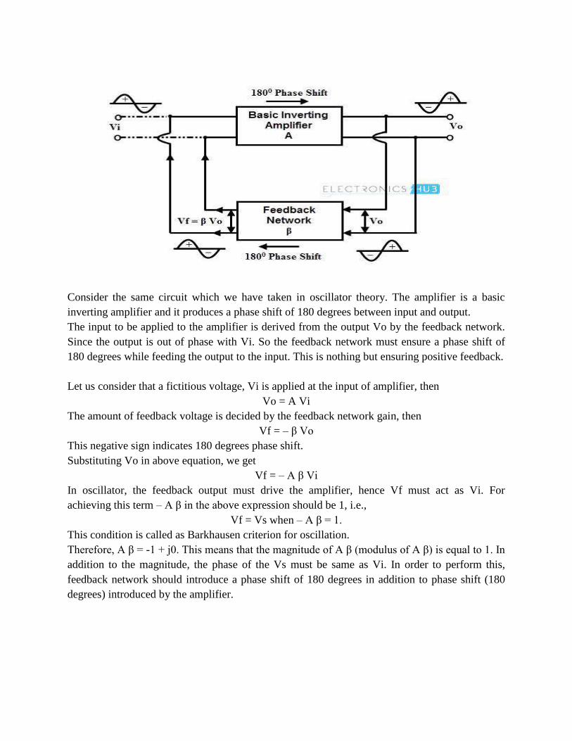
Consider the same circuit which we have taken in oscillator theory. The amplifier is a basic
inverting amplifier and it produces a phase shift of 180 degrees between input and output.
The input to be applied to the amplifier is derived from the output Vo by the feedback network.
Since the output is out of phase with Vi. So the feedback network must ensure a phase shift of
180 degrees while feeding the output to the input. This is nothing but ensuring positive feedback.
Let us consider that a fictitious voltage, Vi is applied at the input of amplifier, then
Vo = A Vi
The amount of feedback voltage is decided by the feedback network gain, then
Vf = – β Vo
This negative sign indicates 180 degrees phase shift.
Substituting Vo in above equation, we get
Vf = – A β Vi
In oscillator, the feedback output must drive the amplifier, hence Vf must act as Vi. For
achieving this term – A β in the above expression should be 1, i.e.,
Vf = Vs when – A β = 1.
This condition is called as Barkhausen criterion for oscillation.
Therefore, A β = -1 + j0. This means that the magnitude of A β (modulus of A β) is equal to 1. In
addition to the magnitude, the phase of the Vs must be same as Vi. In order to perform this,
feedback network should introduce a phase shift of 180 degrees in addition to phase shift (180
degrees) introduced by the amplifier.
www.JntukMaterials.com
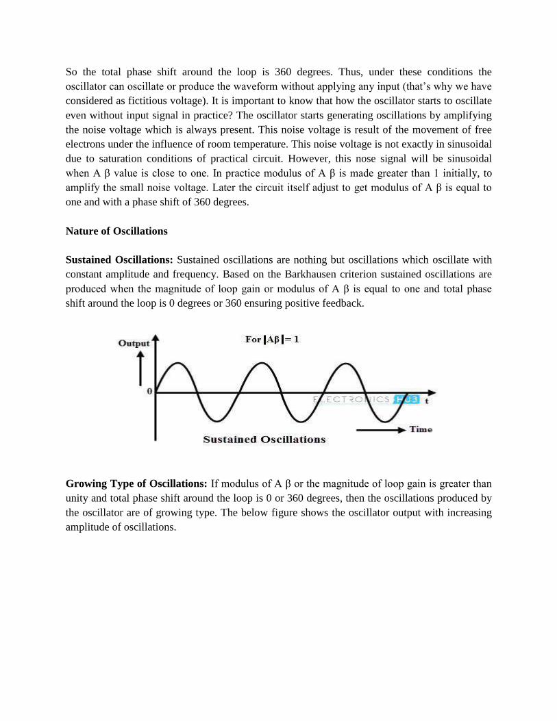
So the total phase shift around the loop is 360 degrees. Thus, under these conditions the
oscillator can oscillate or produce the waveform without applying any input (that’s why we have
considered as fictitious voltage). It is important to know that how the oscillator starts to oscillate
even without input signal in practice? The oscillator starts generating oscillations by amplifying
the noise voltage which is always present. This noise voltage is result of the movement of free
electrons under the influence of room temperature. This noise voltage is not exactly in sinusoidal
due to saturation conditions of practical circuit. However, this nose signal will be sinusoidal
when A β value is close to one. In practice modulus of A β is made greater than 1 initially, to
amplify the small noise voltage. Later the circuit itself adjust to get modulus of A β is equal to
one and with a phase shift of 360 degrees.
Nature of Oscillations
Sustained Oscillations: Sustained oscillations are nothing but oscillations which oscillate with
constant amplitude and frequency. Based on the Barkhausen criterion sustained oscillations are
produced when the magnitude of loop gain or modulus of A β is equal to one and total phase
shift around the loop is 0 degrees or 360 ensuring positive feedback.
Growing Type of Oscillations: If modulus of A β or the magnitude of loop gain is greater than
unity and total phase shift around the loop is 0 or 360 degrees, then the oscillations produced by
the oscillator are of growing type. The below figure shows the oscillator output with increasing
amplitude of oscillations.
www.JntukMaterials.com

Exponentially Decaying Oscillations: If modulus of A β or the magnitude of loop gain is less
than unity and total phase shift around the loop is 0 or 360 degrees, then the amplitude of the
oscillations decreases exponentially and finally these oscillations will cease.
Classification of oscillators
The oscillators are classified into several types based on various factors like nature of waveform,
range of frequency, the parameters used, etc. The following is a broad classification of
oscillators.
According to the Waveform Generated
Based on the output waveform, oscillators are classified as sinusoidal oscillators and non-
sinusoidal oscillators.
Sinusoidal Oscillators: This type of oscillator generates sinusoidal current or voltages.
Non-sinusoidal Oscillators: This type of oscillators generates output, which has triangular,
square, rectangle, saw tooth waveform or is of pulse shape.
According to the Circuit Components: Depends on the usage of components in the circuit,
oscillators are classified into LC, RC and crystal oscillators. The oscillator using inductor and
capacitor components is called as LC oscillator while the oscillator using resistance and
www.JntukMaterials.com

capacitor components is called as RC oscillators. Also, crystal is used in some oscillators which
are called as crystal oscillators.
According to the Frequency Generated: Oscillators can be used to produce the waveforms at
frequencies ranging from low to very high levels. Low frequency or audio frequency oscillators
are used to generate the oscillations at a range of 20 Hz to 100-200 KHz which is an audio
frequency range.
High frequency or radio frequency oscillators are used at the frequencies more than 200-
300 KHz up to gigahertz. LC oscillators are used at high frequency range, whereas RC
oscillators are used at low frequency range.
Based on the Usage of Feedback
The oscillators consisting of feedback network to satisfy the required conditions of the
oscillations are called as feedback oscillators. Whereas the oscillators with absence of feedback
network are called as non-feedback type of oscillators. The UJT relaxation oscillator is the
example of non-feedback oscillator which uses a negative resistance region of the characteristics
of the device.
Some of the sinusoidal oscillators under above categories are
Tuned-circuits or LC feedback oscillators such as Hartley, Colpitts and Clapp etc.
RC phase-shift oscillators such as Wein-bridge oscillator.
Negative-resistance oscillators such as tunnel diode oscillator.
Crystal oscillators such as Pierce oscillator.
Heterodyne or beat-frequency oscillator (BFO).
A single stage amplifier will produce 180o of phase shift between its output and input
signals when connected in a class-A type configuration.
For an oscillator to sustain oscillations indefinitely, sufficient feedback of the correct
phase, that is “Positive Feedback” must be provided along with the transistor amplifier being
used acting as an inverting stage to achieve this.
In an RC Oscillator circuit the input is shifted 180o through the amplifier stage and
180oagain through a second inverting stage giving us “180o + 180o = 360o” of phase shift which
is effectively the same as 0o thereby giving us the required positive feedback. In other words, the
phase shift of the feedback loop should be “0”.
In a Resistance-Capacitance Oscillator or simply an RC Oscillator, we make use of the
fact that a phase shift occurs between the input to a RC network and the output from the same
network by using RC elements in the feedback branch, for example.
www.JntukMaterials.com
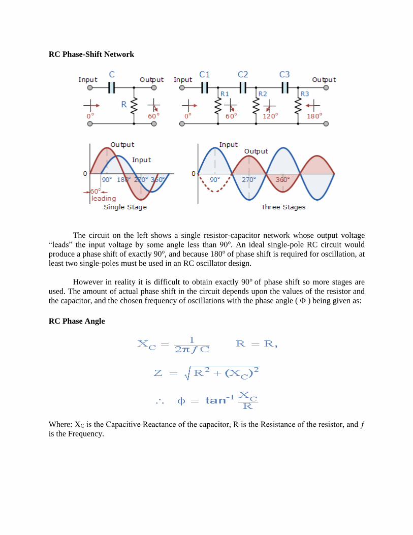
RC Phase-Shift Network
The circuit on the left shows a single resistor-capacitor network whose output voltage
“leads” the input voltage by some angle less than 90o. An ideal single-pole RC circuit would
produce a phase shift of exactly 90o, and because 180o of phase shift is required for oscillation, at
least two single-poles must be used in an RC oscillator design.
However in reality it is difficult to obtain exactly 90o of phase shift so more stages are
used. The amount of actual phase shift in the circuit depends upon the values of the resistor and
the capacitor, and the chosen frequency of oscillations with the phase angle ( Φ ) being given as:
RC Phase Angle
Where: XC is the Capacitive Reactance of the capacitor, R is the Resistance of the resistor, and ƒ
is the Frequency.
www.JntukMaterials.com
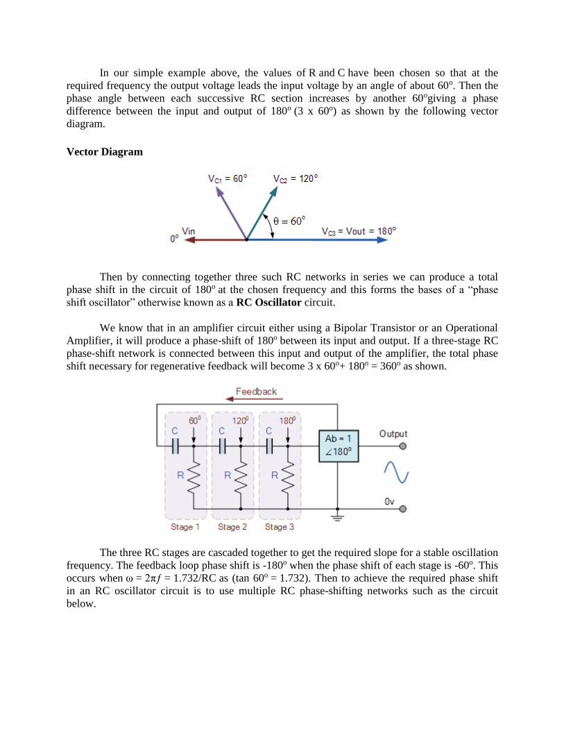
In our simple example above, the values of R and C have been chosen so that at the
required frequency the output voltage leads the input voltage by an angle of about 60o. Then the
phase angle between each successive RC section increases by another 60ogiving a phase
difference between the input and output of 180o (3 x 60o) as shown by the following vector
diagram.
Vector Diagram
Then by connecting together three such RC networks in series we can produce a total
phase shift in the circuit of 180o at the chosen frequency and this forms the bases of a “phase
shift oscillator” otherwise known as a RC Oscillator circuit.
We know that in an amplifier circuit either using a Bipolar Transistor or an Operational
Amplifier, it will produce a phase-shift of 180o between its input and output. If a three-stage RC
phase-shift network is connected between this input and output of the amplifier, the total phase
shift necessary for regenerative feedback will become 3 x 60o+ 180o = 360o as shown.
The three RC stages are cascaded together to get the required slope for a stable oscillation
frequency. The feedback loop phase shift is -180o when the phase shift of each stage is -60o. This
occurs when ω = 2πƒ = 1.732/RC as (tan 60o = 1.732). Then to achieve the required phase shift
in an RC oscillator circuit is to use multiple RC phase-shifting networks such as the circuit
below.
www.JntukMaterials.com
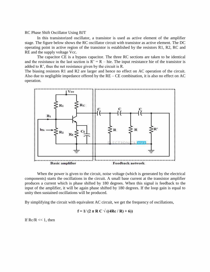
RC Phase Shift Oscillator Using BJT
In this transistorized oscillator, a transistor is used as active element of the amplifier
stage. The figure below shows the RC oscillator circuit with transistor as active element. The DC
operating point in active region of the transistor is established by the resistors R1, R2, RC and
RE and the supply voltage Vcc.
The capacitor CE is a bypass capacitor. The three RC sections are taken to be identical
and the resistance in the last section is R’ = R – hie. The input resistance hie of the transistor is
added to R’, thus the net resistance given by the circuit is R.
The biasing resistors R1 and R2 are larger and hence no effect on AC operation of the circuit.
Also due to negligible impedance offered by the RE – CE combination, it is also no effect on AC
operation.
When the power is given to the circuit, noise voltage (which is generated by the electrical
components) starts the oscillations in the circuit. A small base current at the transistor amplifier
produces a current which is phase shifted by 180 degrees. When this signal is feedback to the
input of the amplifier, it will be again phase shifted by 180 degrees. If the loop gain is equal to
unity then sustained oscillations will be produced.
By simplifying the circuit with equivalent AC circuit, we get the frequency of oscillations,
f = 1/ (2 π R C √ ((4Rc / R) + 6))
If Rc/R << 1, then
www.JntukMaterials.com
f= 1/ (2 π R C √ 6)
The condition of sustained oscillations,
hfe (min) = (4 Rc/ R) + 23 + (29 R/Rc)
For a phase shift oscillator with R = Rc, hfe should be 56 for sustained oscillations.
From the above equations it is clear that, for changing the frequency of oscillations, R and C
values have to be changed.
But for satisfying oscillating conditions, these values of the three sections must be changed
simultaneously. So this is not possible in practice, therefore a phase shift oscillator is used as a
fixed frequency oscillator for all practical purposes.
Advantages of Phase Shift Oscillators:
Due to the absence of expensive and bulky high-value inductors, circuit is simple to
design and well suited for frequencies below 10 KHz.
These can produce pure sinusoidal waveform since only one frequency can fulfill the
Barkhausen phase shift requirement.
It is fixed to one frequency.
Disadvantages of Phase Shift Oscillators:
For a variable frequency usage, phase shift oscillators are not suited because the capacitor values
will have to be varied. And also, for frequency change in every time requires gain adjustment for
satisfying the condition of oscillations.
These oscillators produce 5% of distortion level in the output.
This oscillator gives only a small output due to smaller feedback
These oscillator circuits require a high gain which is practically impossible.
The frequency stability is poor due to the effect of temperature, aging, etc. of various
circuit components.
One of the simplest sine wave oscillators which uses a RC network in place of the
conventional LC tuned tank circuit to produce a sinusoidal output waveform, is called a Wien
Bridge Oscillator.
The Wien Bridge Oscillator is so called because the circuit is based on a frequency-
selective form of the Wheatstone bridge circuit. The Wien Bridge oscillator is a two-
stage RC coupled amplifier circuit that has good stability at its resonant frequency, low distortion
www.JntukMaterials.com

and is very easy to tune making it a popular circuit as an audio frequency oscillator but the phase
shift of the output signal is considerably different from the previous phase shift RC Oscillator.
The Wien Bridge Oscillator uses a feedback circuit consisting of a series RC circuit
connected with a parallel RC of the same component values producing a phase delay or phase
advance circuit depending upon the frequency. At the resonant frequency ƒr the phase shift is 0o.
Consider the circuit below.
RC Phase Shift Network
The above RC network consists of a series RC circuit connected to a parallel RC forming
basically a High Pass Filter connected to a Low Pass Filter producing a very selective second-
order frequency dependant Band Pass Filter with a high Q factor at the selected frequency, ƒr.
At low frequencies the reactance of the series capacitor (C1) is very high so acts like an
open circuit and blocks any input signal at Vin. Therefore there is no output signal, Vout. At high
frequencies, the reactance of the parallel capacitor, (C2) is very low so this parallel connected
capacitor acts like a short circuit on the output so again there is no output signal. However,
between these two extremes the output voltage reaches a maximum value with the frequency at
which this happens being called the Resonant Frequency, (ƒr).
At this resonant frequency, the circuits reactance equals its resistance as Xc = R so the
phase shift between the input and output equals zero degrees. The magnitude of the output
voltage is therefore at its maximum and is equal to one third (1/3) of the input voltage as shown.
www.JntukMaterials.com
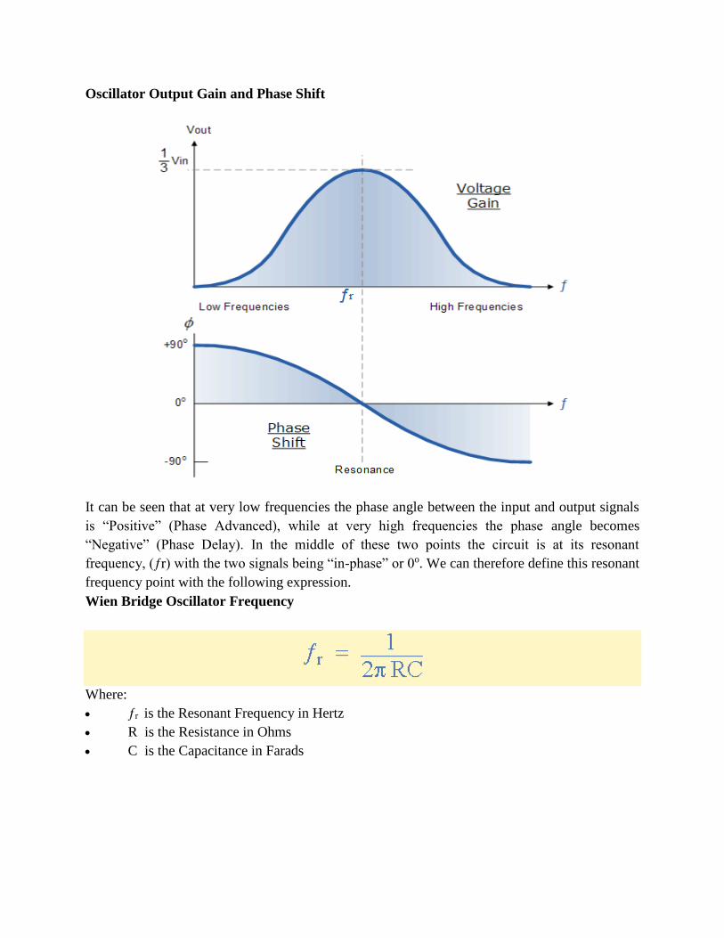
Oscillator Output Gain and Phase Shift
It can be seen that at very low frequencies the phase angle between the input and output signals
is “Positive” (Phase Advanced), while at very high frequencies the phase angle becomes
“Negative” (Phase Delay). In the middle of these two points the circuit is at its resonant
frequency, (ƒr) with the two signals being “in-phase” or 0o. We can therefore define this resonant
frequency point with the following expression.
Wien Bridge Oscillator Frequency
Where:
ƒr is the Resonant Frequency in Hertz
R is the Resistance in Ohms
C is the Capacitance in Farads
www.JntukMaterials.com

We said previously that the magnitude of the output voltage, Vout from the RC network is at its
maximum value and equal to one third (1/3) of the input voltage, Vin to allow for oscillations to
occur. But why one third and not some other value. In order to understand why the output from
the RC circuit above needs to be one-third, that is 0.333xVin, we have to consider the complex
impedance (Z = R ± jX) of the two connected RC circuits.
We know from our AC Theory tutorials that the real part of the complex impedance is
the resistance, R while the imaginary part is the reactance, X. As we are dealing with capacitors
here, the reactance part will be capacitive reactance, Xc.
The RC Network
If we redraw the above RC network as shown, we can clearly see that it consists of two
RC circuits connected together with the output taken from their junction. Resistor R1 and
capacitor C1 form the top series network, while resistor R2 and capacitor C2 form the bottom
parallel network.
Therefore the total impedance of the series combination (R1C1) we can call, ZS and the
total impedance of the parallel combination (R2C2) we can call, ZP. As ZS and ZP are effectively
connected together in series across the input, VIN, they form a voltage divider network with the
output taken from across ZPas shown.
Let’s assume then that the component values of R1 and R2 are the same at: 12kΩ,
capacitors C1 and C2 are the same at: 3.9nF and the supply frequency, ƒ is 3.4kHz.
www.JntukMaterials.com
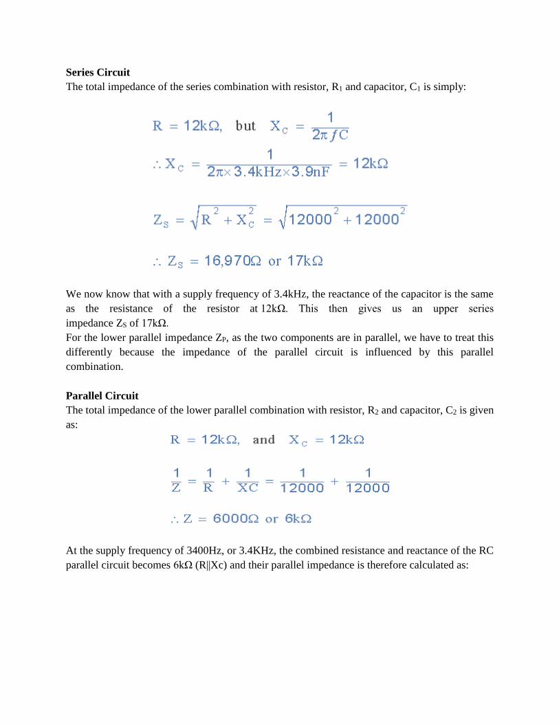
Series Circuit
The total impedance of the series combination with resistor, R1 and capacitor, C1 is simply:
We now know that with a supply frequency of 3.4kHz, the reactance of the capacitor is the same
as the resistance of the resistor at 12kΩ. This then gives us an upper series
impedance ZS of 17kΩ.
For the lower parallel impedance ZP, as the two components are in parallel, we have to treat this
differently because the impedance of the parallel circuit is influenced by this parallel
combination.
Parallel Circuit
The total impedance of the lower parallel combination with resistor, R2 and capacitor, C2 is given
as:
At the supply frequency of 3400Hz, or 3.4KHz, the combined resistance and reactance of the RC
parallel circuit becomes 6kΩ (R||Xc) and their parallel impedance is therefore calculated as:
www.JntukMaterials.com
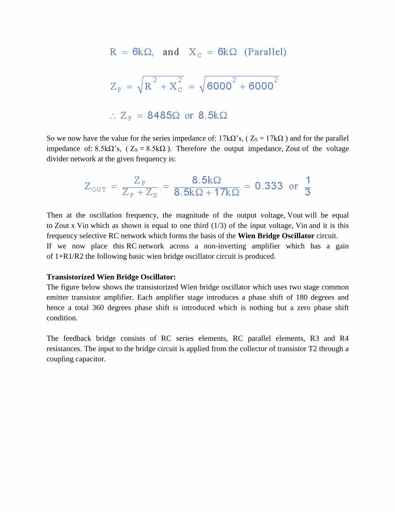
So we now have the value for the series impedance of: 17kΩ’s, ( ZS = 17kΩ ) and for the parallel
impedance of: 8.5kΩ’s, ( ZS = 8.5kΩ ). Therefore the output impedance, Zout of the voltage
divider network at the given frequency is:
Then at the oscillation frequency, the magnitude of the output voltage, Vout will be equal
to Zout x Vin which as shown is equal to one third (1/3) of the input voltage, Vin and it is this
frequency selective RC network which forms the basis of the Wien Bridge Oscillator circuit.
If we now place this RC network across a non-inverting amplifier which has a gain
of 1+R1/R2 the following basic wien bridge oscillator circuit is produced.
Transistorized Wien Bridge Oscillator:
The figure below shows the transistorized Wien bridge oscillator which uses two stage common
emitter transistor amplifier. Each amplifier stage introduces a phase shift of 180 degrees and
hence a total 360 degrees phase shift is introduced which is nothing but a zero phase shift
condition.
The feedback bridge consists of RC series elements, RC parallel elements, R3 and R4
resistances. The input to the bridge circuit is applied from the collector of transistor T2 through a
coupling capacitor.
www.JntukMaterials.com

When the DC source is applied to the circuit, a noise signal is at the base of the transistor T1 is
generated due to the movement of charge carriers through transistor and other circuit
components. This voltage is amplified with gain A and produce output voltage 180 degrees out
of phase with input voltage. This output voltage is applied as input to second transistor at base
terminal of T2. This voltage is multiplied with gain of the T2. The amplified output of the
transistor T2 is 180 degrees out of phase with the output of the T1. This output is feedback to the
transistor T1 through the coupling capacitor C. So the oscillations are produced at wide range of
frequencies by this positive feedback when Barkhausen conditions are satisfied. Generally, the
Wien bridge in the feedback network incorporates the oscillations at single desired frequency.
The bridge is get balanced at the frequency at which total phase shift is zero.
The output of the two stage transistor acts as an input to the feedback network which is applied
between the base and ground.
Feedback voltage,
Vf = (Vo × R4) / (R3 + R4)
Advantages:
Because of the usage of two stage amplifier, the overall gain of this oscillator is high.
By varying the values of C1 and C2 or with use of variable resistors, the frequency of
oscillations can be varied.
It produces a very good sine wave with less distortion
The frequency stability is good.
Due to the absence of inductors, no interference occurs from external magnetic fields.
www.JntukMaterials.com

Disadvantages:
More number of components is needed for two stage amplifier type of Wien bridge
oscillators.
Very high frequencies cannot be generated.
In many ways, the Colpitts oscillator is the exact opposite of the Hartley Oscillator we
looked at in the previous tutorial. Just like the Hartley oscillator, the tuned tank circuit consists of
an LC resonance sub-circuit connected between the collector and the base of a single stage
transistor amplifier producing a sinusoidal output waveform. The basic configuration of
the Colpitts Oscillator resembles that of the Hartley Oscillator but the difference this time is
that the centre tapping of the tank sub-circuit is now made at the junction of a “capacitive voltage
divider” network instead of a tapped autotransformer type inductor as in the Hartley oscillator.
Related Products: Oscillators and Crystals | Controlled Oscillator | MEMS Oscillators | Oscillator
Misc | Silicon Oscillators
Colpitts Oscillator:
Tank Circuit:
The Colpitts oscillator uses a capacitive voltage divider network as its feedback source.
The two capacitors, C1 and C2 are placed across a single common inductor, L as shown.
Then C1, C2 and L form the tuned tank circuit with the condition for oscillations
being: XC1 + XC2 = XL, the same as for the Hartley oscillator circuit. The advantage of this type
of capacitive circuit configuration is that with less self and mutual inductance within the tank
circuit, frequency stability of the oscillator is improved along with a more simple design. As with
the Hartley oscillator, the Colpitts oscillator uses a single stage bipolar transistor amplifier as the
gain element which produces a sinusoidal output. Consider the circuit below.
www.JntukMaterials.com

Basic Colpitts Oscillator Circuit
The emitter terminal of the transistor is effectively connected to the junction of the two
capacitors, C1 and C2 which are connected in series and act as a simple voltage divider. When
the power supply is firstly applied, capacitors C1 and C2 charge up and then discharge through
the coil L. The oscillations across the capacitors are applied to the base-emitter junction and
appear in the amplified at the collector output.
Resistors, R1 and R2 provide the usual stabilizing DC bias for the transistor in the normal
manner while the additional capacitors act as a DC-blocking bypass capacitors. A radio-
frequency choke (RFC) is used in the collector circuit to provide a high reactance (ideally open
circuit) at the frequency of oscillation, ( ƒr ) and a low resistance at DC to help start the
oscillations.
The required external phase shift is obtained in a similar manner to that in the Hartley oscillator
circuit with the required positive feedback obtained for sustained undamped oscillations. The
amount of feedback is determined by the ratio of C1 and C2. These two capacitances are
generally “ganged” together to provide a constant amount of feedback so that as one is adjusted
the other automatically follows.
www.JntukMaterials.com

The frequency of oscillations for a Colpitts oscillator is determined by the resonant frequency of
the LC tank circuit and is given as:
Where CT is the capacitance of C1 and C2 connected in series and is given as:
The configuration of the transistor amplifier is of a Common Emitter Amplifier with the output
signal 180o out of phase with regards to the input signal. The additional 180ophase shift require
for oscillation is achieved by the fact that the two capacitors are connected together in series but
in parallel with the inductive coil resulting in overall phase shift of the circuit being zero or 360o.
The amount of feedback depends on the values of C1 and C2. We can see that the voltage
across C1 is the the same as the oscillators output voltage, Vout and that the voltage across C2 is
the oscillators feedback voltage. Then the voltage across C1 will be much greater than that
across C2.
Therefore, by changing the values of capacitors, C1 and C2 we can adjust the amount of
feedback voltage returned to the tank circuit. However, large amounts of feedback may cause the
output sine wave to become distorted, while small amounts of feedback may not allow the circuit
to oscillate.
Then the amount of feedback developed by the Colpitts oscillator is based on the capacitance
ratio of C1 and C2 and is what governs the the excitation of the oscillator. This ratio is called the
“feedback fraction” and is given simply as:
www.JntukMaterials.com
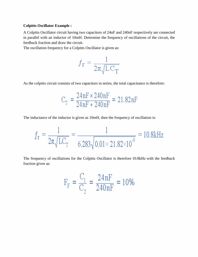
Colpitts Oscillator Example :
A Colpitts Oscillator circuit having two capacitors of 24nF and 240nF respectively are connected
in parallel with an inductor of 10mH. Determine the frequency of oscillations of the circuit, the
feedback fraction and draw the circuit.
The oscillation frequency for a Colpitts Oscillator is given as:
As the colpitts circuit consists of two capacitors in series, the total capacitance is therefore:
The inductance of the inductor is given as 10mH, then the frequency of oscillation is:
The frequency of oscillations for the Colpitts Oscillator is therefore 10.8kHz with the feedback
fraction given as:
www.JntukMaterials.com
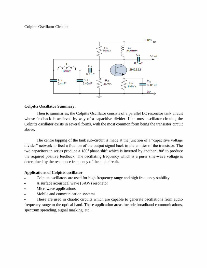
Colpitts Oscillator Circuit:
Colpitts Oscillator Summary:
Then to summaries, the Colpitts Oscillator consists of a parallel LC resonator tank circuit
whose feedback is achieved by way of a capacitive divider. Like most oscillator circuits, the
Colpitts oscillator exists in several forms, with the most common form being the transistor circuit
above.
The centre tapping of the tank sub-circuit is made at the junction of a “capacitive voltage
divider” network to feed a fraction of the output signal back to the emitter of the transistor. The
two capacitors in series produce a 180o phase shift which is inverted by another 180o to produce
the required positive feedback. The oscillating frequency which is a purer sine-wave voltage is
determined by the resonance frequency of the tank circuit.
Applications of Colpitts oscillator
Colpitts oscillators are used for high frequency range and high frequency stability
A surface acoustical wave (SAW) resonator
Microwave applications
Mobile and communication systems
These are used in chaotic circuits which are capable to generate oscillations from audio
frequency range to the optical band. These application areas include broadband communications,
spectrum spreading, signal masking, etc.
www.JntukMaterials.com
One of the main disadvantages of the basic LC Oscillator circuit we looked at in the
previous tutorial is that they have no means of controlling the amplitude of the oscillations and
also, it is difficult to tune the oscillator to the required frequency. If the cumulative
electromagnetic coupling between L1 and L2 is too small there would be insufficient feedback
and the oscillations would eventually die away to zero.
Likewise if the feedback was too strong the oscillations would continue to increase in
amplitude until they were limited by the circuit conditions producing signal distortion. So it
becomes very difficult to “tune” the oscillator. However, it is possible to feed back exactly the
right amount of voltage for constant amplitude oscillations. If we feed back more than is
necessary the amplitude of the oscillations can be controlled by biasing the amplifier in such a
way that if the oscillations increase in amplitude, the bias is increased and the gain of the
amplifier is reduced. If the amplitude of the oscillations decreases the bias decreases and the gain
of the amplifier increases, thus increasing the feedback. In this way the amplitude of the
oscillations are kept constant using a process known as Automatic Base Bias.
One big advantage of automatic base bias in a voltage controlled oscillator, is that the
oscillator can be made more efficient by providing a Class-B bias or even a Class-C bias
condition of the transistor. This has the advantage that the collector current only flows during
part of the oscillation cycle so the quiescent collector current is very small. Then this “self-
tuning” base oscillator circuit forms one of the most common types of LC parallel resonant
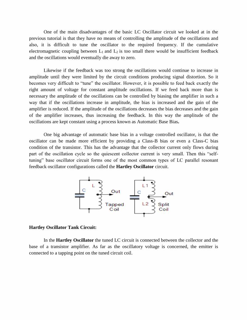
feedback oscillator configurations called the Hartley Oscillator circuit.
Hartley Oscillator Tank Circuit:
In the Hartley Oscillator the tuned LC circuit is connected between the collector and the
base of a transistor amplifier. As far as the oscillatory voltage is concerned, the emitter is
connected to a tapping point on the tuned circuit coil.
www.JntukMaterials.com

The feedback part of the tuned LC tank circuit is taken from the centre tap of the inductor
coil or even two separate coils in series which are in parallel with a variable capacitor, C as
shown.
The Hartley circuit is often referred to as a split-inductance oscillator because coil L is
centre-tapped. In effect, inductance L acts like two separate coils in very close proximity with
the current flowing through coil section XY induces a signal into coil section YZ below.
An Hartley Oscillator circuit can be made from any configuration that uses either a single
tapped coil (similar to an autotransformer) or a pair of series connected coils in parallel with a
single capacitor as shown below.
Basic Hartley Oscillator Design
When the circuit is oscillating, the voltage at point X (collector), relative to
point Y (emitter), is 180o out-of-phase with the voltage at point Z (base) relative to point Y. At
the frequency of oscillation, the impedance of the Collector load is resistive and an increase in
Base voltage causes a decrease in the Collector voltage.
Then there is a 180o phase change in the voltage between the Base and Collector and this
along with the original 180o phase shift in the feedback loop provides the correct phase
relationship of positive feedback for oscillations to be maintained.
The amount of feedback depends upon the position of the “tapping point” of the inductor.
If this is moved nearer to the collector the amount of feedback is increased, but the output taken
between the Collector and earth is reduced and vice versa. Resistors, R1 and R2 provide the
www.JntukMaterials.com

usual stabilizing DC bias for the transistor in the normal manner while the capacitors act as DC-
blocking capacitors.
In this Hartley Oscillator circuit, the DC Collector current flows through part of the coil
and for this reason the circuit is said to be “Series-fed” with the frequency of oscillation of the
Hartley Oscillator being given as.
Note: LT is the total cumulatively coupled inductance if two separate coils are used including
their mutual inductance, M.
The frequency of oscillations can be adjusted by varying the “tuning” capacitor, C or by varying
the position of the iron-dust core inside the coil (inductive tuning) giving an output over a wide
range of frequencies making it very easy to tune. Also the Hartley Oscillator produces an output
amplitude which is constant over the entire frequency range.
As well as the Series-fed Hartley Oscillator above, it is also possible to connect the tuned tank
circuit across the amplifier as a shunt-fed oscillator as shown below.
Shunt-fed Hartley Oscillator Circuit:
In the shunt-fed Hartley oscillator circuit, both the AC and DC components of the
Collector current have separate paths around the circuit. Since the DC component is blocked by
www.JntukMaterials.com
the capacitor, C2 no DC flows through the inductive coil, L and less power is wasted in the tuned
circuit.
The Radio Frequency Coil (RFC), L2 is an RF choke which has a high reactance at the
frequency of oscillations so that most of the RF current is applied to the LC tuning tank circuit
via capacitor, C2 as the DC component passes through L2 to the power supply. A resistor could
be used in place of the RFC coil, L2 but the efficiency would be less.
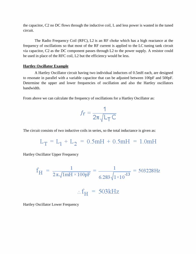
Hartley Oscillator Example
A Hartley Oscillator circuit having two individual inductors of 0.5mH each, are designed
to resonate in parallel with a variable capacitor that can be adjusted between 100pF and 500pF.
Determine the upper and lower frequencies of oscillation and also the Hartley oscillators
bandwidth.
From above we can calculate the frequency of oscillations for a Hartley Oscillator as:
The circuit consists of two inductive coils in series, so the total inductance is given as:
Hartley Oscillator Upper Frequency
Hartley Oscillator Lower Frequency
www.JntukMaterials.com
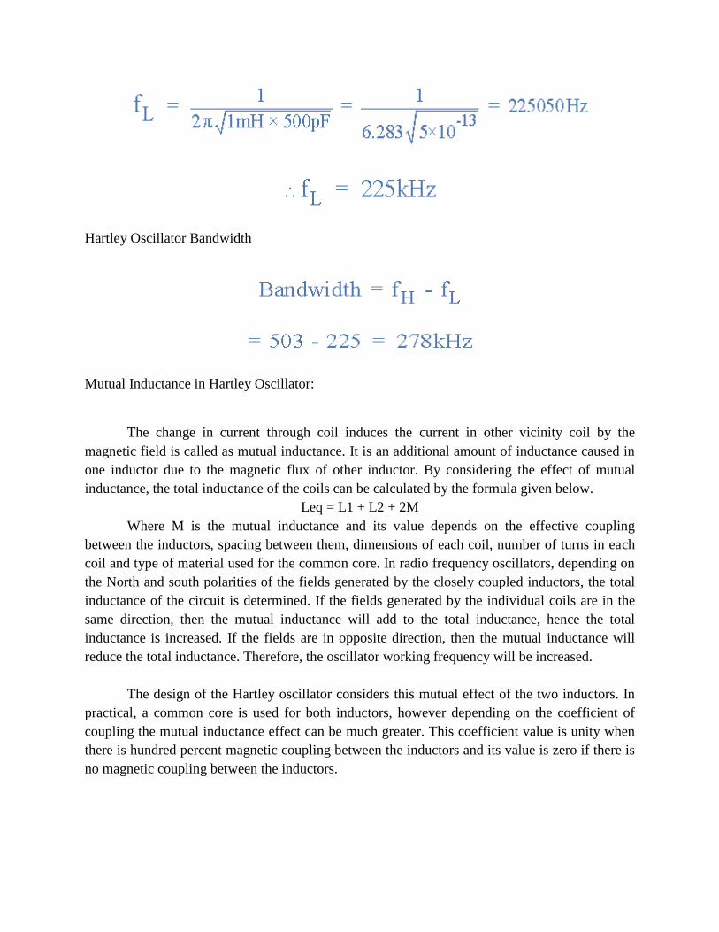
Hartley Oscillator Bandwidth
Mutual Inductance in Hartley Oscillator:
The change in current through coil induces the current in other vicinity coil by the
magnetic field is called as mutual inductance. It is an additional amount of inductance caused in
one inductor due to the magnetic flux of other inductor. By considering the effect of mutual
inductance, the total inductance of the coils can be calculated by the formula given below.
Leq = L1 + L2 + 2M
Where M is the mutual inductance and its value depends on the effective coupling
between the inductors, spacing between them, dimensions of each coil, number of turns in each
coil and type of material used for the common core. In radio frequency oscillators, depending on
the North and south polarities of the fields generated by the closely coupled inductors, the total
inductance of the circuit is determined. If the fields generated by the individual coils are in the
same direction, then the mutual inductance will add to the total inductance, hence the total
inductance is increased. If the fields are in opposite direction, then the mutual inductance will
reduce the total inductance. Therefore, the oscillator working frequency will be increased.
The design of the Hartley oscillator considers this mutual effect of the two inductors. In
practical, a common core is used for both inductors, however depending on the coefficient of
coupling the mutual inductance effect can be much greater. This coefficient value is unity when
there is hundred percent magnetic coupling between the inductors and its value is zero if there is
no magnetic coupling between the inductors.
www.JntukMaterials.com

The Hartley Oscillator Summary:
Then to summarize, the Hartley Oscillator consists of a parallel LC resonator tank circuit whose
feedback is achieved by way of an inductive divider. Like most oscillator circuits, the Hartley
oscillator exists in several forms, with the most common form being the transistor circuit above.
This Hartley Oscillator configuration has a tuned tank circuit with its resonant coil tapped to
feed a fraction of the output signal back to the emitter of the transistor. Since the output of the
transistors emitter is always “in-phase” with the output at the collector, this feedback signal is
positive. The oscillating frequency which is a sine-wave voltage is determined by the resonance
frequency of the tank circuit.
In the next tutorial about Oscillators, we will look at another type of LC oscillator circuit that is
the opposite to the Hartley oscillator called the Colpitts oscillator. The Colpitts oscillator uses
two capacitors in series to form a centre tapped capacitance in parallel with a single inductance
within its resonant tank circuit.
When a constant voltage but of varying frequency is applied to a circuit consisting of an
inductor, capacitor and resistor the reactance of both the Capacitor/Resistor and
Inductor/Resistor circuits is to change both the amplitude and the phase of the output signal as
compared to the input signal due to the reactance of the components used. At high frequencies
the reactance of a capacitor is very low acting as a short circuit while the reactance of the
inductor is high acting as an open circuit. At low frequencies the reverse is true, the reactance of
the capacitor acts as an open circuit and the reactance of the inductor acts as a short circuit.
Between these two extremes the combination of the inductor and capacitor produces a “Tuned”
or “Resonant” circuit that has a Resonant Frequency, ( ƒr ) in which the capacitive and
inductive reactance’s are equal and cancel out each other, leaving only the resistance of the
circuit to oppose the flow of current. This means that there is no phase shift as the current is in
phase with the voltage. Consider the circuit below.
Basic LC Oscillator Tank Circuit:
www.JntukMaterials.com

The circuit consists of an inductive coil, L and a capacitor, C. The capacitor stores energy
in the form of an electrostatic field and which produces a potential (static voltage) across its
plates, while the inductive coil stores its energy in the form of an electromagnetic field. The
capacitor is charged up to the DC supply voltage, V by putting the switch in position A.
When the capacitor is fully charged the switch changes to position B. The charged
capacitor is now connected in parallel across the inductive coil so the capacitor begins to
discharge itself through the coil. The voltage across C starts falling as the current through the
coil begins to rise. This rising current sets up an electromagnetic field around the coil which
resists this flow of current. When the capacitor, C is completely discharged the energy that was
originally stored in the capacitor, C as an electrostatic field is now stored in the inductive
coil, L as an electromagnetic field around the coils windings. As there is now no external voltage
in the circuit to maintain the current within the coil, it starts to fall as the electromagnetic field
begins to collapse. A back emf is induced in the coil (e = -Ldi/dt) keeping the current flowing in
the original direction. These current charges up capacitor, C with the opposite polarity to its
original charge. C continues to charge up until the current reduces to zero and the
electromagnetic field of the coil has collapsed completely.
The energy originally introduced into the circuit through the switch, has been returned to
the capacitor which again has an electrostatic voltage potential across it, although it is now of the
opposite polarity. The capacitor now starts to discharge again back through the coil and the
whole process is repeated. The polarity of the voltage changes as the energy is passed back and
forth between the capacitor and inductor producing an AC type sinusoidal voltage and current
waveform. This process then forms the basis of an LC oscillators tank circuit and theoretically
this cycling back and forth will continue indefinitely.
However, things are not perfect and every time energy is transferred from the
capacitor, C to inductor, L and back from L to C some energy losses occur which decay the
oscillations to zero over time. This oscillatory action of passing energy back and forth between
the capacitor, C to the inductor, L would continue indefinitely if it was not for energy losses
within the circuit. Electrical energy is lost in the DC or real resistance of the inductors coil, in the
dielectric of the capacitor, and in radiation from the circuit so the oscillation steadily decreases
until they die away completely and the process stops. Then in a practical LC circuit the
amplitude of the oscillatory voltage decreases at each half cycle of oscillation and will eventually
die away to zero. The oscillations are then said to be “damped” with the amount of damping
being determined by the quality or Q-factor of the circuit.
www.JntukMaterials.com

Damped Oscillations
The frequency of the oscillatory voltage depends upon the value of the inductance and
capacitance in the LC tank circuit. We now know that for resonance to occur in the tank circuit,
there must be a frequency point were the value of XC, the capacitive reactance is the same as the
value of XL, the inductive reactance ( XL = XC ) and which will therefore cancel out each other
out leaving only the DC resistance in the circuit to oppose the flow of current. If we now place
the curve for inductive reactance of the inductor on top of the curve for capacitive reactance of
the capacitor so that both curves are on the same frequency axes, the point of intersection will
give us the resonance frequency point, ( ƒr or ωr ) as shown below.
Resonance Frequency
www.JntukMaterials.com
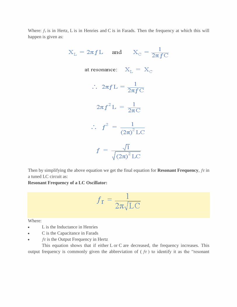
Where: ƒr is in Hertz, L is in Henries and C is in Farads. Then the frequency at which this will
happen is given as:
Then by simplifying the above equation we get the final equation for Resonant Frequency, ƒr in
a tuned LC circuit as:
Resonant Frequency of a LC Oscillator:
Where:
L is the Inductance in Henries
C is the Capacitance in Farads
ƒr is the Output Frequency in Hertz
This equation shows that if either L or C are decreased, the frequency increases. This
output frequency is commonly given the abbreviation of ( ƒr ) to identify it as the “resonant
www.JntukMaterials.com

frequency”.To keep the oscillations going in an LC tank circuit, we have to replace all the energy
lost in each oscillation and also maintain the amplitude of these oscillations at a constant level.
The amount of energy replaced must therefore be equal to the energy lost during each cycle.
If the energy replaced is too large the amplitude would increase until clipping of the
supply rails occurs. Alternatively, if the amount of energy replaced is too small the amplitude
would eventually decrease to zero over time and the oscillations would stop. The simplest way of
replacing this lost energy is to take part of the output from the LC tank circuit, amplify it and
then feed it back into the LC circuit again. This process can be achieved using a voltage
amplifier using an op-amp, FET or bipolar transistor as its active device. However, if the loop
gain of the feedback amplifier is too small, the desired oscillation decays to zero and if it is too
large, the waveform becomes distorted.
To produce a constant oscillation, the level of the energy fed back to the LC network
must be accurately controlled. Then there must be some form of automatic amplitude or gain
control when the amplitude tries to vary from a reference voltage either up or down.To maintain
a stable oscillation the overall gain of the circuit must be equal to one or unity. Any less and the
oscillations will not start or die away to zero, any more the oscillations will occur but the
amplitude will become clipped by the supply rails causing distortion. Consider the circuit below.
Basic Transistor LC Oscillator Circuit
A Bipolar Transistor is used as the LC oscillator’s amplifier with the tuned LC tank circuit acts
as the collector load. Another coil L2 is connected between the base and the emitter of the
transistor whose electromagnetic field is “mutually” coupled with that of coil L.
www.JntukMaterials.com
“Mutual inductance” exists between the two circuits and the changing current flowing in one coil
circuit induces, by electromagnetic induction, a potential voltage in the other (transformer effect)
so as the oscillations occur in the tuned circuit, electromagnetic energy is transferred from
coil L to coil L2 and a voltage of the same frequency as that in the tuned circuit is applied
between the base and emitter of the transistor. In this way the necessary automatic feedback
voltage is applied to the amplifying transistor.
The amount of feedback can be increased or decreased by altering the coupling between the two
coils L and L2. When the circuit is oscillating its impedance is resistive and the collector and
base voltages are 180o out of phase. In order to maintain oscillations (called frequency stability)
the voltage applied to the tuned circuit must be “in-phase” with the oscillations occurring in the
tuned circuit.
Therefore, we must introduce an additional 180o phase shift into the feedback path between the
collector and the base. This is achieved by winding the coil of L2 in the correct direction relative
to coil L giving us the correct amplitude and phase relationships for the Oscillators circuit or by
connecting a phase shift network between the output and input of the amplifier. The LC
Oscillator is therefore a “Sinusoidal Oscillator” or a “Harmonic Oscillator” as it is more
commonly called. LC oscillators can generate high frequency sine waves for use in radio
frequency (RF) type applications with the transistor amplifier being of a Bipolar Transistor or
FET.
Harmonic Oscillators come in many different forms because there are many different ways to
construct an LC filter network and amplifier with the most common being the Hartley LC
Oscillator, Colpitts LC Oscillator, Armstrong Oscillator and Clapp Oscillator to name a
few.
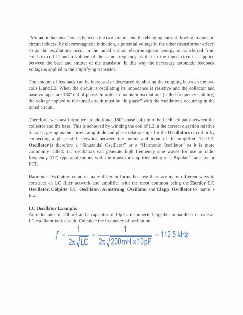
LC Oscillator Example:
An inductance of 200mH and a capacitor of 10pF are connected together in parallel to create an
LC oscillator tank circuit. Calculate the frequency of oscillation.
www.JntukMaterials.com

Then we can see from the above example that by decreasing the value of either the
capacitance, C or the inductance, L will have the effect of increasing the frequency of oscillation
of the LC tank circuit.
LC Oscillators Summary:
The basic conditions required for an LC oscillator resonant tank circuit are given as follows.
For oscillations to exist an oscillator circuit MUST contain a reactive (frequency-
dependant) component either an “Inductor”, (L) or a “Capacitor”, (C) as well as a DC power
source.
In a simple inductor-capacitor, LC circuit, oscillations become damped over time due
to component and circuit losses.
Voltage amplification is required to overcome these circuit losses and provide positive
gain.
The overall gain of the amplifier must be greater than one, unity.
Oscillations can be maintained by feeding back some of the output voltage to the
tuned circuit that is of the correct amplitude and in-phase, (0o).
Oscillations can only occur when the feedback is “Positive” (self-regeneration).
The overall phase shift of the circuit must be zero or 360o so that the output signal
from the feedback network will be “in-phase” with the input signal.
UNIT-V
Power Amplifiers:
Classification of amplifiers, Class A power Amplifiers and their analysis, Harmonic Distortions,
Class B Push-pull amplifiers and their analysis, Complementary symmetry push pull amplifier,
www.JntukMaterials.com