this document is downloaded from the digital open access ... · citation: journal of vacuum science...
TRANSCRIPT
This document is downloaded from the Digital Open Access Repository of VTT
VTT
http://www.vtt.fi P.O. box 1000 FI-02044 VTT Finland
By using VTT Digital Open Access Repository you are bound by the following Terms & Conditions.
I have read and I understand the following statement:
This document is protected by copyright and other intellectual property rights, and duplication or sale of all or part of any of this document is not permitted, except duplication for research use or educational purposes in electronic or print form. You must obtain permission for any other use. Electronic or print copies may not be offered for sale.
Title Microscopic silicon-based lateral high-aspect-ratio
structures for thin film conformality analysis
Author(s) Gao, Feng; Arpiainen, Sanna; Puurunen, Riikka L.
Citation Journal of Vacuum Science and Technology A:
Vacuum, Surfaces and Films. American Vacuum
Society. Vol. 33 (2015) No: 1, 010601
Date 2015
URL http://dx.doi.org/10.1116/1.4903941
Rights This article may be downloaded for personal use
only.

Microscopic silicon-based lateral high-aspect-ratio structures for thin film conformalityanalysisFeng Gao, Sanna Arpiainen, and Riikka L. Puurunen Citation: Journal of Vacuum Science & Technology A 33, 010601 (2015); doi: 10.1116/1.4903941 View online: http://dx.doi.org/10.1116/1.4903941 View Table of Contents: http://scitation.aip.org/content/avs/journal/jvsta/33/1?ver=pdfcov Published by the AVS: Science & Technology of Materials, Interfaces, and Processing Articles you may be interested in High aspect ratio iridescent three-dimensional metal–insulator–metal capacitors using atomic layer deposition J. Vac. Sci. Technol. A 33, 01A103 (2015); 10.1116/1.4891319 Structural analysis of Au/TiO2 thin films deposited on the glass substrate Appl. Phys. Lett. 102, 091603 (2013); 10.1063/1.4794842 Permeation measurements and modeling of highly defective Al 2 O 3 thin films grown by atomic layer depositionon polymers Appl. Phys. Lett. 97, 221901 (2010); 10.1063/1.3519476 Highly conformal film growth by chemical vapor deposition. II. Conformality enhancement through growthinhibition J. Vac. Sci. Technol. A 27, 1244 (2009); 10.1116/1.3207746 Chemical and structural properties of atomic layer deposited La 2 O 3 films capped with a thin Al 2 O 3 layer J. Vac. Sci. Technol. A 27, L1 (2009); 10.1116/1.3079632
Redistribution subject to AVS license or copyright; see http://scitation.aip.org/termsconditions. Download to IP: 130.188.8.27 On: Thu, 08 Jan 2015 09:08:48

LETTERS
Microscopic silicon-based lateral high-aspect-ratio structures for thin filmconformality analysis
Feng Gao, Sanna Arpiainen, and Riikka L. Puurunena)
VTT Technical Research Centre of Finland, Tietotie 3, 02044 Espoo, Finland
(Received 30 September 2014; accepted 1 December 2014; published 15 December 2014)
Film conformality is one of the major drivers for the interest in atomic layer deposition (ALD)
processes. This work presents new silicon-based microscopic lateral high-aspect-ratio (LHAR) test
structures for the analysis of the conformality of thin films deposited by ALD and by other
chemical vapor deposition means. The microscopic LHAR structures consist of a lateral cavity
inside silicon with a roof supported by pillars. The cavity length (e.g., 20–5000 lm) and cavity
height (e.g., 200–1000 nm) can be varied, giving aspect ratios of, e.g., 20:1 to 25 000:1. Film
conformality can be analyzed with the microscopic LHAR by several means, as demonstrated for
the ALD Al2O3 and TiO2 processes from Me3Al/H2O and TiCl4/H2O. The microscopic LHAR
test structures introduced in this work expose a new parameter space for thin film conformality
investigations expected to prove useful in the development, tuning and modeling of ALD and other
chemical vapor deposition processes. VC 2014 American Vacuum Society.
[http://dx.doi.org/10.1116/1.4903941]
I. INTRODUCTION
Atomic layer deposition (ALD) is a thin film deposition
method based on the use of repeated self-terminating (i.e.,
saturating and irreversible) chemisorption reactions.1–3 It is
already used in several industrial applications such as thin
film electroluminescent displays, dynamic random-access
memories and complementary metal–oxide–semiconductor
field effect transistors.4,5 As a multitool of nanotechnology,
ALD attracts interest in highly different fields of applications
from catalysis to coatings for flexible electronics and from
textiles to photovoltaics.
One of the key drivers for the interest in ALD is the ability
to grow conformal films, which are uniform in thickness on
complex-shaped three-dimensional (3D) substrates even when
the thickness is a fraction of a nanometer (or even a fraction
of a monolayer). Conformality of ALD films is a general
assumption and a direct result of the ideal self-terminating
ALD chemistry. Nevertheless, even for the most ideal ALD
processes, pulsing sequences need to be adjusted from those
used for planar substrates, to achieve a uniform coating inside
demanding 3D features.6,7 Also, many processes developed as
ALD in the laboratory scale and tabulated in review articles8
may contain secondary reaction paths of irreversible reactant
decomposition and undesired side-reactions of the reactants
or the gaseous reaction products,9 which decrease the film
conformality in 3D features and may even prevent the
up-scaling of the process to industrial scale.10
One reason for the fact that most ALD process studies are
carried out on planar substrates, without reporting on the film
conformality, may be the lack of test structures, which would
be easy to use, simple to analyze, and readily available.
When conformality is investigated, it is most often done in
vertical trenches etched into the silicon substrates—either
with a modest depth-to-width aspect ratio (AR) of roughly,
e.g., 5:1 (Ref. 3) or more demanding AR of about 40:1.11,12
With macroscopic lateral high-aspect-ratio (LHAR) test
structures,13,14 accurate thickness profiles along the gap have
been recorded with AR up to 200:1. Because of the macro-
scopic dimensions (gap size on the order of 100 lm), molecu-
lar flow inside these LHAR structures is reached only in high
vacuum (e.g., 10�4 Torr).
In this work, we present a new type of a silicon-based
microscopic LHAR test structure for thin film conformality
analysis. The limiting dimension of the structure is in the
hundreds of nanometers range. This allows the assumption of
molecular flow for the typical ALD pressure ranges (one to
tens of millibars), as at these pressures the mean free path of
molecules on the order of micrometers to tens of micro-
meters. We demonstrate the use of the microscopic LHAR
test structures ALD thin film conformality analysis in diverse
ways, from regular microscopy to thickness line scans and
electron microscopy. The ALD Al2O3 and TiO2 processes
from Me3Al/TiCl4 and H2O reactants are used for testing, as
these are among the oldest and most studied ALD processes.8
II. EXPERIMENT
The LHAR structures, shown schematically in Fig. 1,
were fabricated on 150 mm silicon wafers using the standard
surface micromachining techniques. First, a thermal oxide
layer, defining the gap height of the cavity (200, 500, and
1000 nm), was grown on the polished silicon surface. Next, a
a)Author to whom correspondence should be addressed; electronic mail:
010601-1 J. Vac. Sci. Technol. A 33(1), Jan/Feb 2015 0734-2101/2015/33(1)/010601/5/$30.00 VC 2014 American Vacuum Society 010601-1
Redistribution subject to AVS license or copyright; see http://scitation.aip.org/termsconditions. Download to IP: 130.188.8.27 On: Thu, 08 Jan 2015 09:08:48
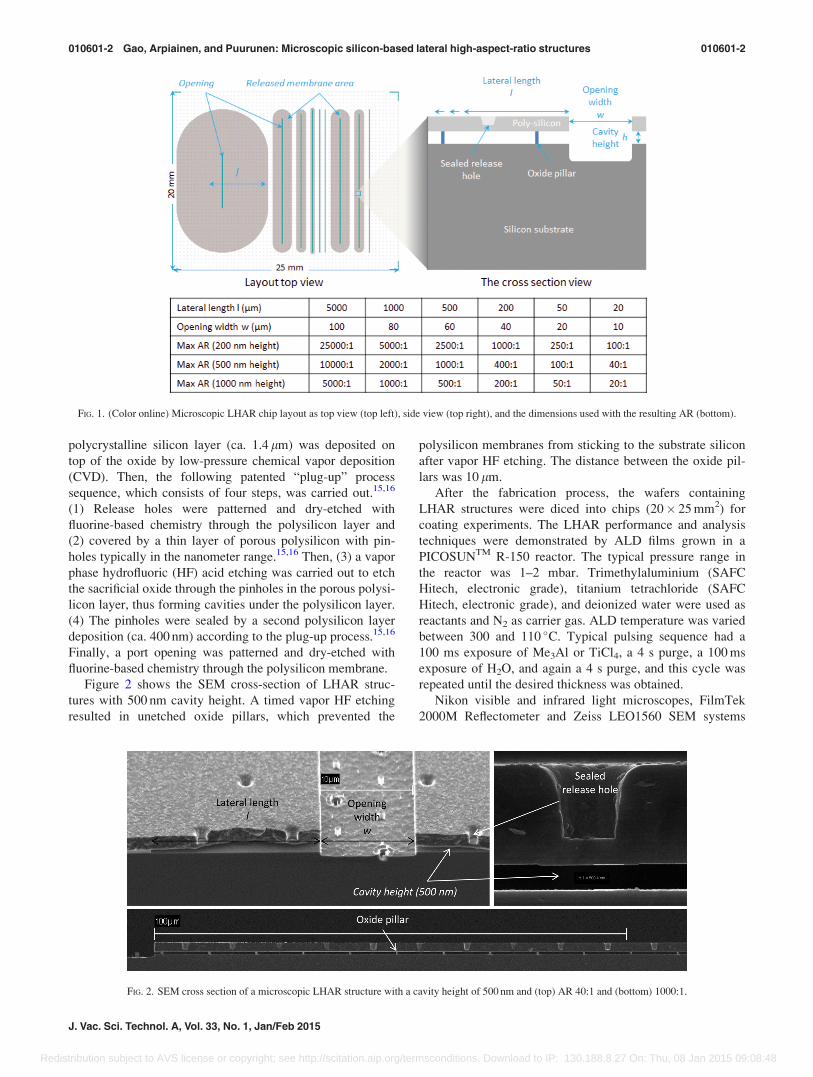
polycrystalline silicon layer (ca. 1.4 lm) was deposited on
top of the oxide by low-pressure chemical vapor deposition
(CVD). Then, the following patented “plug-up” process
sequence, which consists of four steps, was carried out.15,16
(1) Release holes were patterned and dry-etched with
fluorine-based chemistry through the polysilicon layer and
(2) covered by a thin layer of porous polysilicon with pin-
holes typically in the nanometer range.15,16 Then, (3) a vapor
phase hydrofluoric (HF) acid etching was carried out to etch
the sacrificial oxide through the pinholes in the porous polysi-
licon layer, thus forming cavities under the polysilicon layer.
(4) The pinholes were sealed by a second polysilicon layer
deposition (ca. 400 nm) according to the plug-up process.15,16
Finally, a port opening was patterned and dry-etched with
fluorine-based chemistry through the polysilicon membrane.
Figure 2 shows the SEM cross-section of LHAR struc-
tures with 500 nm cavity height. A timed vapor HF etching
resulted in unetched oxide pillars, which prevented the
polysilicon membranes from sticking to the substrate silicon
after vapor HF etching. The distance between the oxide pil-
lars was 10 lm.
After the fabrication process, the wafers containing
LHAR structures were diced into chips (20� 25 mm2) for
coating experiments. The LHAR performance and analysis
techniques were demonstrated by ALD films grown in a
PICOSUNTM R-150 reactor. The typical pressure range in
the reactor was 1–2 mbar. Trimethylaluminium (SAFC
Hitech, electronic grade), titanium tetrachloride (SAFC
Hitech, electronic grade), and deionized water were used as
reactants and N2 as carrier gas. ALD temperature was varied
between 300 and 110 �C. Typical pulsing sequence had a
100 ms exposure of Me3Al or TiCl4, a 4 s purge, a 100 ms
exposure of H2O, and again a 4 s purge, and this cycle was
repeated until the desired thickness was obtained.
Nikon visible and infrared light microscopes, FilmTek
2000M Reflectometer and Zeiss LEO1560 SEM systems
FIG. 1. (Color online) Microscopic LHAR chip layout as top view (top left), side view (top right), and the dimensions used with the resulting AR (bottom).
FIG. 2. SEM cross section of a microscopic LHAR structure with a cavity height of 500 nm and (top) AR 40:1 and (bottom) 1000:1.
010601-2 Gao, Arpiainen, and Puurunen: Microscopic silicon-based lateral high-aspect-ratio structures 010601-2
J. Vac. Sci. Technol. A, Vol. 33, No. 1, Jan/Feb 2015
Redistribution subject to AVS license or copyright; see http://scitation.aip.org/termsconditions. Download to IP: 130.188.8.27 On: Thu, 08 Jan 2015 09:08:48
were used to analyze the uncoated and coated microscopic
LHAR structures. The reflectometer has a spot size of about
5� 5 lm2 with 50� magnification.
III. RESULTS AND DISCUSSION
A. Nondestructive optical top-view analysis
The microscopic LHAR structures consist of a cavity
under a thin silicon membrane, with a center opening to
allow the penetration of gases for thin film growth. The
extent of the film growth under the membrane can be investi-
gated nondestructively through the membrane, for example,
by visible-light microscopy as well as by infrared
microscopy.
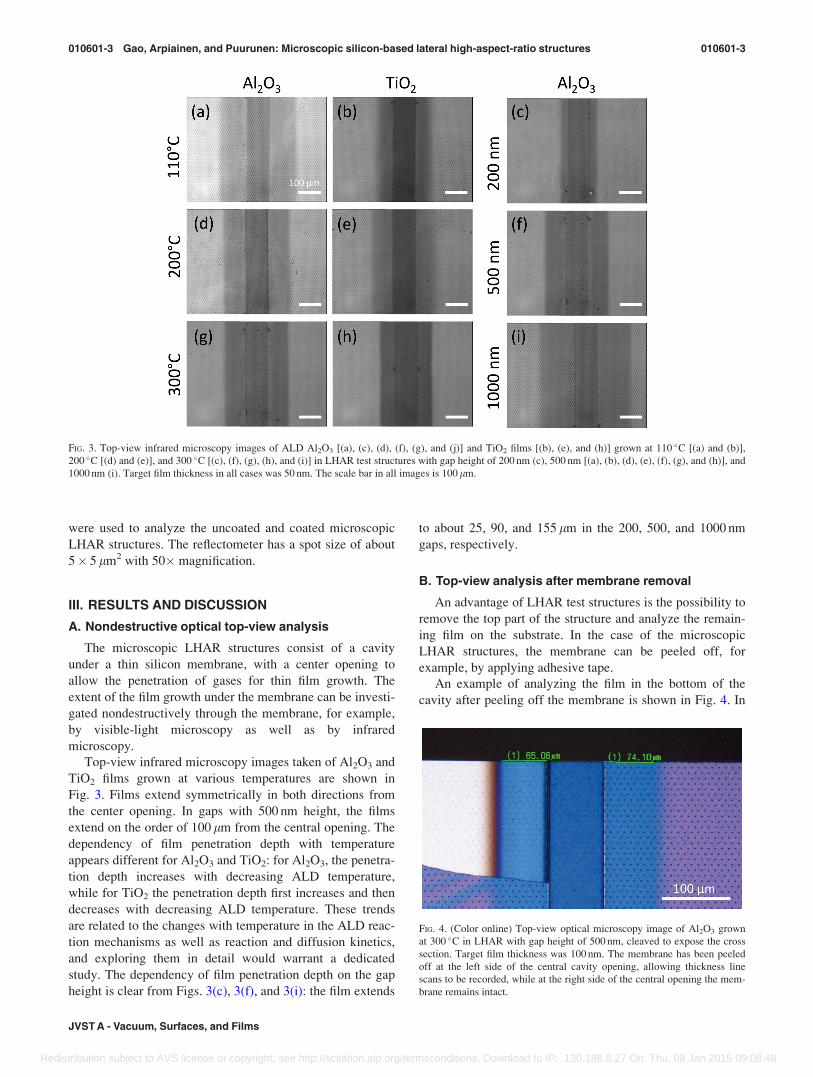
Top-view infrared microscopy images taken of Al2O3 and
TiO2 films grown at various temperatures are shown in
Fig. 3. Films extend symmetrically in both directions from
the center opening. In gaps with 500 nm height, the films
extend on the order of 100 lm from the central opening. The
dependency of film penetration depth with temperature
appears different for Al2O3 and TiO2: for Al2O3, the penetra-
tion depth increases with decreasing ALD temperature,
while for TiO2 the penetration depth first increases and then
decreases with decreasing ALD temperature. These trends
are related to the changes with temperature in the ALD reac-
tion mechanisms as well as reaction and diffusion kinetics,
and exploring them in detail would warrant a dedicated
study. The dependency of film penetration depth on the gap
height is clear from Figs. 3(c), 3(f), and 3(i): the film extends
to about 25, 90, and 155 lm in the 200, 500, and 1000 nm
gaps, respectively.
B. Top-view analysis after membrane removal
An advantage of LHAR test structures is the possibility to
remove the top part of the structure and analyze the remain-
ing film on the substrate. In the case of the microscopic
LHAR structures, the membrane can be peeled off, for
example, by applying adhesive tape.
An example of analyzing the film in the bottom of the
cavity after peeling off the membrane is shown in Fig. 4. In
FIG. 3. Top-view infrared microscopy images of ALD Al2O3 [(a), (c), (d), (f), (g), and (j)] and TiO2 films [(b), (e), and (h)] grown at 110 �C [(a) and (b)],
200 �C [(d) and (e)], and 300 �C [(c), (f), (g), (h), and (i)] in LHAR test structures with gap height of 200 nm (c), 500 nm [(a), (b), (d), (e), (f), (g), and (h)], and
1000 nm (i). Target film thickness in all cases was 50 nm. The scale bar in all images is 100 lm.
FIG. 4. (Color online) Top-view optical microscopy image of Al2O3 grown
at 300 �C in LHAR with gap height of 500 nm, cleaved to expose the cross
section. Target film thickness was 100 nm. The membrane has been peeled
off at the left side of the central cavity opening, allowing thickness line
scans to be recorded, while at the right side of the central opening the mem-
brane remains intact.
010601-3 Gao, Arpiainen, and Puurunen: Microscopic silicon-based lateral high-aspect-ratio structures 010601-3
JVST A - Vacuum, Surfaces, and Films
Redistribution subject to AVS license or copyright; see http://scitation.aip.org/termsconditions. Download to IP: 130.188.8.27 On: Thu, 08 Jan 2015 09:08:48
this case, the silicon LHAR chip was cleaved in order to ex-
pose the cross section for electron microscopy analysis. On
the left, the film under the membrane has been exposed. The
penetration of the film inside the cavity can be easily meas-
ured by visible-light microscope. In this case, the film
extends about 65 lm (AR 130:1) inside the cavity, having
the blue interference color typical for a 100 nm Al2O3 film
on Si. Beyond this point, the transition of the film interfer-
ence color through brown at 80 lm (corresponding to
�50 nm film thickness) to colorless at 90 lm reveals the
decrease of film thickness and, eventually, a bare silicon
surface. The ending profile of the film is soft, and it takes
tens of micrometers for the thickness to decrease to below
the detection level.
Perhaps the most powerful means of using the LHAR test
structure is to make thickness line scans after the membrane
has been peeled off. In the case of the microscopic LHAR
test structures, the spot size of needs to be sufficiently small
to obtain lateral thickness information.
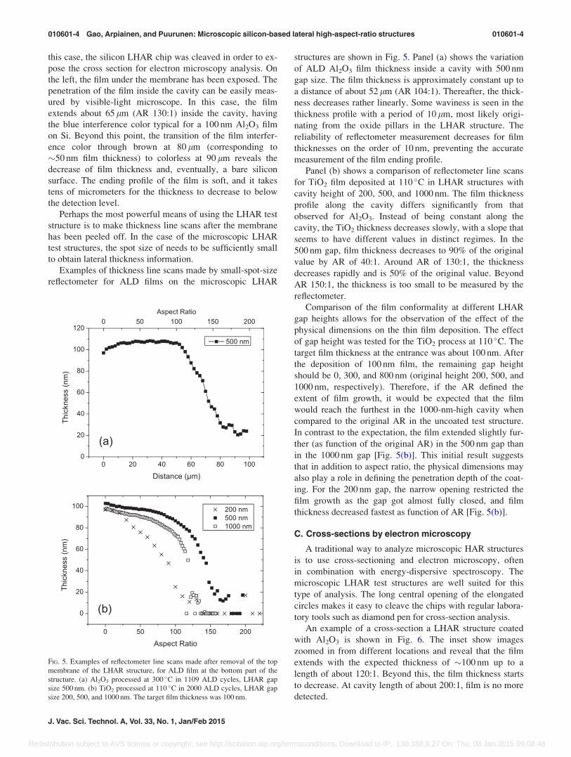
Examples of thickness line scans made by small-spot-size
reflectometer for ALD films on the microscopic LHAR
structures are shown in Fig. 5. Panel (a) shows the variation
of ALD Al2O3 film thickness inside a cavity with 500 nm
gap size. The film thickness is approximately constant up to
a distance of about 52 lm (AR 104:1). Thereafter, the thick-
ness decreases rather linearly. Some waviness is seen in the
thickness profile with a period of 10 lm, most likely origi-
nating from the oxide pillars in the LHAR structure. The
reliability of reflectometer measurement decreases for film
thicknesses on the order of 10 nm, preventing the accurate
measurement of the film ending profile.
Panel (b) shows a comparison of reflectometer line scans
for TiO2 film deposited at 110 �C in LHAR structures with
cavity height of 200, 500, and 1000 nm. The film thickness
profile along the cavity differs significantly from that
observed for Al2O3. Instead of being constant along the
cavity, the TiO2 thickness decreases slowly, with a slope that
seems to have different values in distinct regimes. In the
500 nm gap, film thickness decreases to 90% of the original
value by AR of 40:1. Around AR of 130:1, the thickness
decreases rapidly and is 50% of the original value. Beyond
AR 150:1, the thickness is too small to be measured by the
reflectometer.
Comparison of the film conformality at different LHAR
gap heights allows for the observation of the effect of the
physical dimensions on the thin film deposition. The effect
of gap height was tested for the TiO2 process at 110 �C. The
target film thickness at the entrance was about 100 nm. After
the deposition of 100 nm film, the remaining gap height
should be 0, 300, and 800 nm (original height 200, 500, and
1000 nm, respectively). Therefore, if the AR defined the
extent of film growth, it would be expected that the film
would reach the furthest in the 1000-nm-high cavity when
compared to the original AR in the uncoated test structure.
In contrast to the expectation, the film extended slightly fur-
ther (as function of the original AR) in the 500 nm gap than
in the 1000 nm gap [Fig. 5(b)]. This initial result suggests
that in addition to aspect ratio, the physical dimensions may
also play a role in defining the penetration depth of the coat-
ing. For the 200 nm gap, the narrow opening restricted the
film growth as the gap got almost fully closed, and film
thickness decreased fastest as function of AR [Fig. 5(b)].
C. Cross-sections by electron microscopy
A traditional way to analyze microscopic HAR structures
is to use cross-sectioning and electron microscopy, often
in combination with energy-dispersive spectroscopy. The
microscopic LHAR test structures are well suited for this
type of analysis. The long central opening of the elongated
circles makes it easy to cleave the chips with regular labora-
tory tools such as diamond pen for cross-section analysis.
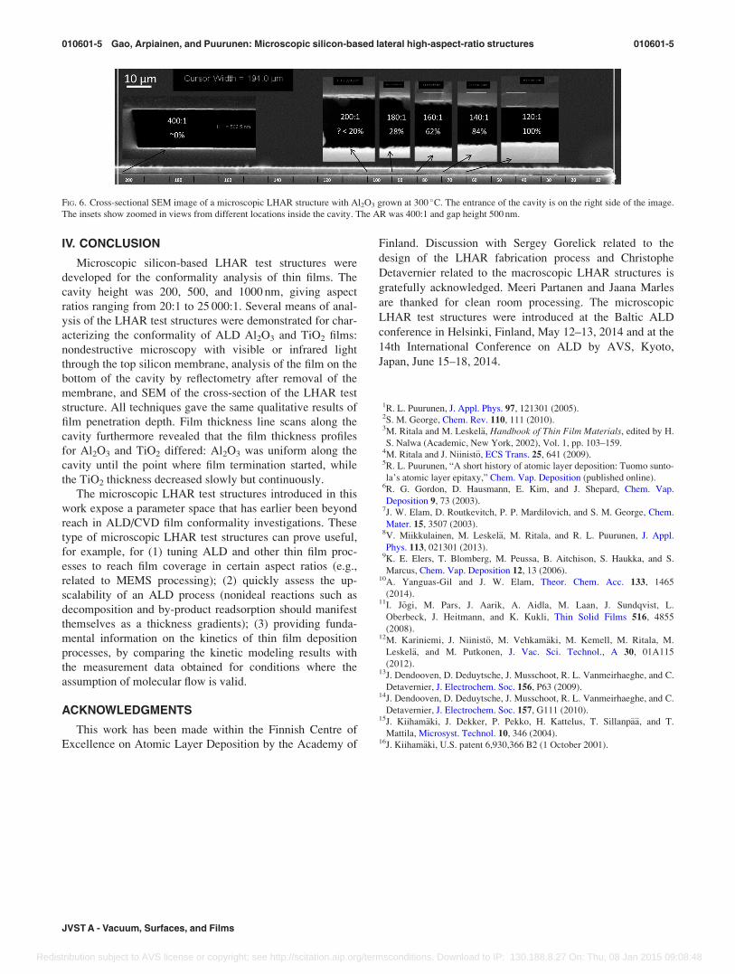
An example of a cross-section a LHAR structure coated
with Al2O3 is shown in Fig. 6. The inset show images
zoomed in from different locations and reveal that the film
extends with the expected thickness of �100 nm up to a
length of about 120:1. Beyond this, the film thickness starts
to decrease. At cavity length of about 200:1, film is no more
detected.
FIG. 5. Examples of reflectometer line scans made after removal of the top
membrane of the LHAR structure, for ALD film at the bottom part of the
structure. (a) Al2O3 processed at 300 �C in 1109 ALD cycles, LHAR gap
size 500 nm. (b) TiO2 processed at 110 �C in 2000 ALD cycles, LHAR gap
size 200, 500, and 1000 nm. The target film thickness was 100 nm.
010601-4 Gao, Arpiainen, and Puurunen: Microscopic silicon-based lateral high-aspect-ratio structures 010601-4
J. Vac. Sci. Technol. A, Vol. 33, No. 1, Jan/Feb 2015
Redistribution subject to AVS license or copyright; see http://scitation.aip.org/termsconditions. Download to IP: 130.188.8.27 On: Thu, 08 Jan 2015 09:08:48
IV. CONCLUSION
Microscopic silicon-based LHAR test structures were
developed for the conformality analysis of thin films. The
cavity height was 200, 500, and 1000 nm, giving aspect
ratios ranging from 20:1 to 25 000:1. Several means of anal-
ysis of the LHAR test structures were demonstrated for char-
acterizing the conformality of ALD Al2O3 and TiO2 films:
nondestructive microscopy with visible or infrared light
through the top silicon membrane, analysis of the film on the
bottom of the cavity by reflectometry after removal of the
membrane, and SEM of the cross-section of the LHAR test
structure. All techniques gave the same qualitative results of
film penetration depth. Film thickness line scans along the
cavity furthermore revealed that the film thickness profiles
for Al2O3 and TiO2 differed: Al2O3 was uniform along the
cavity until the point where film termination started, while
the TiO2 thickness decreased slowly but continuously.
The microscopic LHAR test structures introduced in this
work expose a parameter space that has earlier been beyond
reach in ALD/CVD film conformality investigations. These
type of microscopic LHAR test structures can prove useful,
for example, for (1) tuning ALD and other thin film proc-
esses to reach film coverage in certain aspect ratios (e.g.,
related to MEMS processing); (2) quickly assess the up-
scalability of an ALD process (nonideal reactions such as
decomposition and by-product readsorption should manifest
themselves as a thickness gradients); (3) providing funda-
mental information on the kinetics of thin film deposition
processes, by comparing the kinetic modeling results with
the measurement data obtained for conditions where the
assumption of molecular flow is valid.
ACKNOWLEDGMENTS
This work has been made within the Finnish Centre of
Excellence on Atomic Layer Deposition by the Academy of
Finland. Discussion with Sergey Gorelick related to the
design of the LHAR fabrication process and Christophe
Detavernier related to the macroscopic LHAR structures is
gratefully acknowledged. Meeri Partanen and Jaana Marles
are thanked for clean room processing. The microscopic
LHAR test structures were introduced at the Baltic ALD
conference in Helsinki, Finland, May 12–13, 2014 and at the
14th International Conference on ALD by AVS, Kyoto,
Japan, June 15–18, 2014.
1R. L. Puurunen, J. Appl. Phys. 97, 121301 (2005).2S. M. George, Chem. Rev. 110, 111 (2010).3M. Ritala and M. Leskel€a, Handbook of Thin Film Materials, edited by H.
S. Nalwa (Academic, New York, 2002), Vol. 1, pp. 103–159.4M. Ritala and J. Niinist€o, ECS Trans. 25, 641 (2009).5R. L. Puurunen, “A short history of atomic layer deposition: Tuomo sunto-
la’s atomic layer epitaxy,” Chem. Vap. Deposition (published online).6R. G. Gordon, D. Hausmann, E. Kim, and J. Shepard, Chem. Vap.
Deposition 9, 73 (2003).7J. W. Elam, D. Routkevitch, P. P. Mardilovich, and S. M. George, Chem.
Mater. 15, 3507 (2003).8V. Miikkulainen, M. Leskel€a, M. Ritala, and R. L. Puurunen, J. Appl.
Phys. 113, 021301 (2013).9K. E. Elers, T. Blomberg, M. Peussa, B. Aitchison, S. Haukka, and S.
Marcus, Chem. Vap. Deposition 12, 13 (2006).10A. Yanguas-Gil and J. W. Elam, Theor. Chem. Acc. 133, 1465
(2014).11I. J~ogi, M. Pars, J. Aarik, A. Aidla, M. Laan, J. Sundqvist, L.
Oberbeck, J. Heitmann, and K. Kukli, Thin Solid Films 516, 4855
(2008).12M. Kariniemi, J. Niinist€o, M. Vehkam€aki, M. Kemell, M. Ritala, M.
Leskel€a, and M. Putkonen, J. Vac. Sci. Technol., A 30, 01A115
(2012).13J. Dendooven, D. Deduytsche, J. Musschoot, R. L. Vanmeirhaeghe, and C.
Detavernier, J. Electrochem. Soc. 156, P63 (2009).14J. Dendooven, D. Deduytsche, J. Musschoot, R. L. Vanmeirhaeghe, and C.
Detavernier, J. Electrochem. Soc. 157, G111 (2010).15J. Kiiham€aki, J. Dekker, P. Pekko, H. Kattelus, T. Sillanp€a€a, and T.
Mattila, Microsyst. Technol. 10, 346 (2004).16J. Kiiham€aki, U.S. patent 6,930,366 B2 (1 October 2001).
FIG. 6. Cross-sectional SEM image of a microscopic LHAR structure with Al2O3 grown at 300 �C. The entrance of the cavity is on the right side of the image.
The insets show zoomed in views from different locations inside the cavity. The AR was 400:1 and gap height 500 nm.
010601-5 Gao, Arpiainen, and Puurunen: Microscopic silicon-based lateral high-aspect-ratio structures 010601-5
JVST A - Vacuum, Surfaces, and Films
Redistribution subject to AVS license or copyright; see http://scitation.aip.org/termsconditions. Download to IP: 130.188.8.27 On: Thu, 08 Jan 2015 09:08:48