ti designs compact full hd 1080p (up to 16 amps ... · design using dlp® pico™ technology ......
TRANSCRIPT
TIDUC88 – August 2016 TIDA-01226 1
Copyright © 2016, Texas Instruments Incorporated
TI Designs Compact Full HD 1080p (up to 16 Amps) Projection Display Reference Design using DLP® Pico™ Technology
Design Overview
This reference design, featuring the DLP® Pico™
0.47-inch TRP Full-HD 1080p display chipset and implemented in the DLP LightCrafter Display 4710 G2 evaluation module (EVM), enables use of full HD resolution for projection display applications such as accessory projectors, screenless displays, interactive displays, wearables (including head mounted displays), signage, industrial and medical displays. The chipset used in the design is comprised of the DLP4710 (.47 1080p) DMD, the DLPC3439 display controller and the DLPA3005 PMIC/LED driver Design Resources
TIDA-01226 Design Folder
DLPC3439 Product Folder
DLP4710 Product Folder
DLPA3005 Product Folder
TIDA-00576 Tools Folder
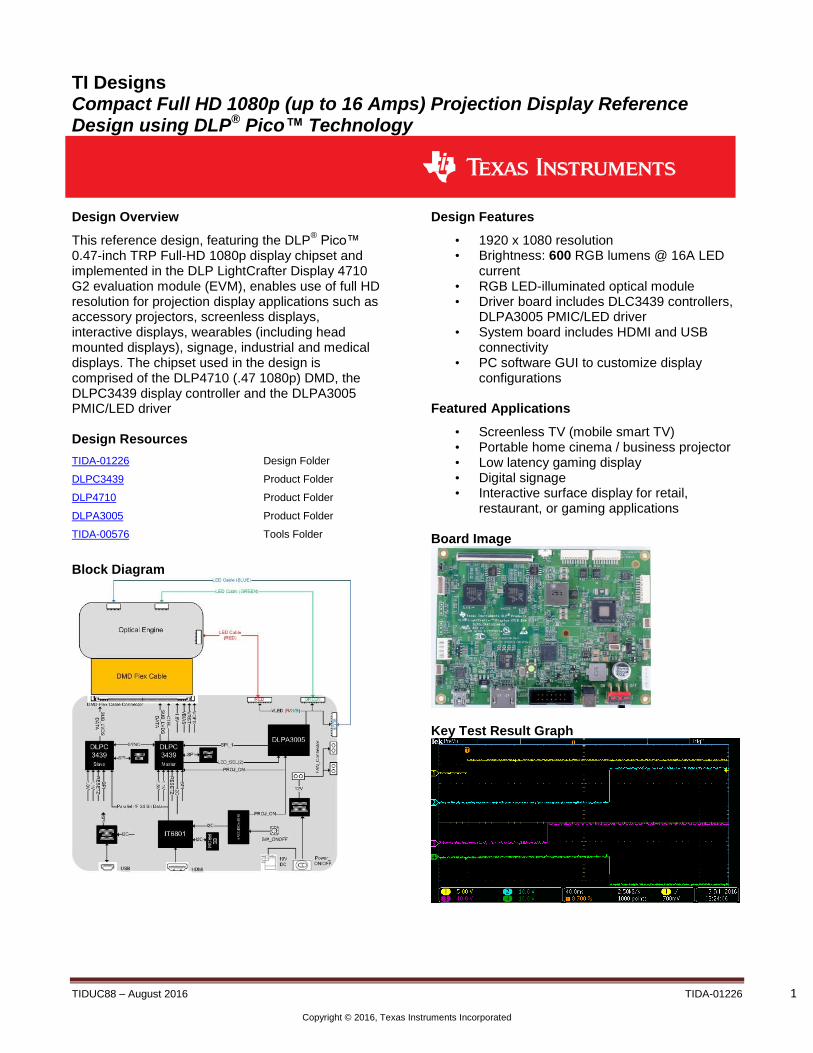
Block Diagram
Design Features
• 1920 x 1080 resolution • Brightness: 600 RGB lumens @ 16A LED
current • RGB LED-illuminated optical module • Driver board includes DLC3439 controllers,
DLPA3005 PMIC/LED driver • System board includes HDMI and USB
connectivity • PC software GUI to customize display
configurations Featured Applications
• Screenless TV (mobile smart TV) • Portable home cinema / business projector • Low latency gaming display • Digital signage • Interactive surface display for retail,
restaurant, or gaming applications Board Image
Key Test Result Graph

www.ti.com
TIDUC88 - August 2016 TIDA-01226 2
Copyright © 2016, Texas Instruments Incorporated
1 Key System Specifications
The DLP LightCrafter Display module consists of three subsystems:
1. Light engine – includes the optics, red, green, blue LEDs and a 1920 x 1080 (1080p) DMD
capable of 600 lumens out-of-the-box.
Figure 1: Optical engine specification
2. DLP Driver – includes the DLP chipset comprising of DLPC3439 Controller and DLPA3005
PMIC/LED driver with up to 16A LED current.
3. System front end – includes MSP430, ITE HDMI receiver, USB-Serial Bridge Controller and
several connectors for external inputs (HDMI, USB, etc.)
2 System Description
2.1 DLPC3439
The 2x DLPC3439 digital controllers, part of the DLP4710 (.47 1080p) chipset, supports reliable operation of the DLP4710 digital micromirror device (DMD). The DLPC3439 controller provides a convenient, multi-functional interface between system electronics and the DMD, enabling small form factor, low power, and high resolution full HD displays.
Figure 2: Functional Block Diagram
Parameter Min Typ. Max Unit
Brightness @ Red 12A / Green 16A / Blue 16A LED current
600 Lum
Red LED Current 12 A
Green / Blue LED Current 16 A
Brightness Uniformity 73 %
Offset 100 %
Focus Range (Wide) 40 120 inch
Image diagonal size 40 100 inch

www.ti.com
TIDUC88 - August 2016 TIDA-01226 3
Copyright © 2016, Texas Instruments Incorporated
2.2 DLPA3005
The DLPA3005 is a highly-integrated power management IC optimized for DLP™ Pico ™Projector systems. The DLPA3005 supports LED projectors up to 16 A per LED, enabled by an integrated high efficiency buck controller. Additionally, the drivers control the RGB switches, supporting the sequencing of R, G, and B LEDs. The DLPA3005 contains five buck converters, two of which are dedicated for DLPC low voltage supplies. Another dedicated regulating supply generates the three timing-critical DC supplies for the DMD: VBIAS, VRST, and VOFS. The DLPA3005 contains several auxiliary blocks which can be used in a flexible way. This enables a tailor-made Pico Projector system. Three 8-bit programmable buck converters can be used, for instance, to drive projector FANs or to make auxiliary supply lines. Two LDOs can be used for a lower-current supply, up to 200 mA. These LDOs are pre-defined to 2.5 V and 3.3 V. Through the SPI, all blocks of the DLPA3005 can be addressed. Features included are the generation of the system reset, power sequencing, input signals for sequentially selecting the active LED, IC self-protections, and an analog MUX for routing analog information to an external ADC.
Figure 3: System Block Diagram
2.3 DLP4710
The DLP4710 digital micromirror device (DMD) is a digitally controlled micro-opto-electromechanical system (MEMS) spatial light modulator (SLM). When coupled to an appropriate optical system, the DLP4710 DMD displays a very crisp and high quality image or video. DLP4710 is part of the chipset comprising of the DLP4710 DMD, DLPC3439 display controller and DLPA3000/DLPA3005 PMIC/LED drivers. The compact physical size of the DLP4710 coupled with the controller and the PMIC/LED driver provides a complete system solution that enables small form factor, low power, and high resolution HD displays.
www.ti.com
TIDUC88 - August 2016 TIDA-01226 4
Copyright © 2016, Texas Instruments Incorporated
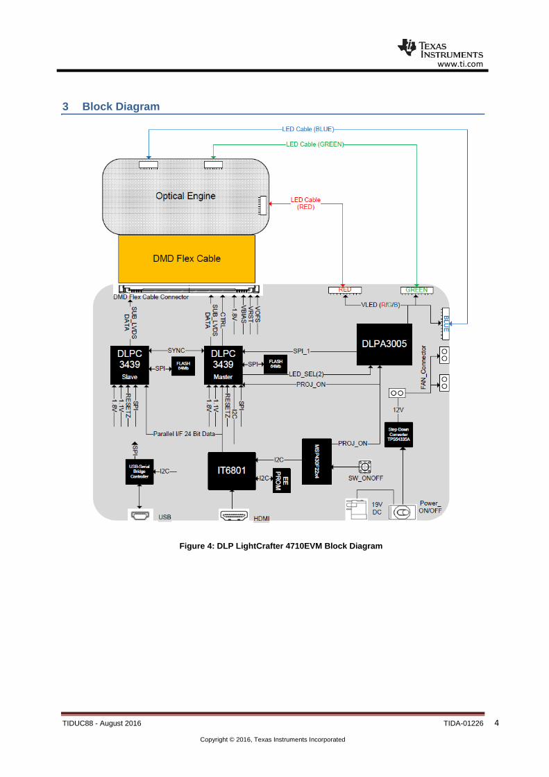
3 Block Diagram
Figure 4: DLP LightCrafter 4710EVM Block Diagram

www.ti.com
TIDUC88 - August 2016 TIDA-01226 5
Copyright © 2016, Texas Instruments Incorporated
3.1 Highlighted Products
3.1.1 DLPC3439 Features
Supports Input Image Sizes up to 1080p
24 Bit, Input Pixel Interface Support: o Parallel Interface o Pixel Clock up to 150MHz
Pixel Data Processing o IntelliBright™ Suite of Image Processing Algorithms o Image Resizing (Scaling) o Color Coordinate Adjustment o Programmable Degamma o Active Power Management Processing o Color Space Conversion
Auto DMD Parking at Power Down
Compatible with the DLPA3000 and DLPA3005 PMIC/LED Drivers
3.1.2 DLPA3005 Features
High-Efficiency, High-Current RGB LED Driver
Drivers for External Buck FETs up to 16 A
Drivers for External RGB Switches
10-Bit Programmable Current per Channel
Inputs for Selecting Color-Sequential RGB LEDs
Generation of DMD High Voltage Supplies
Two High Efficiency Buck Converters to Generate the DLPC343x and DMD Supply
Three High Efficiency, 8-Bit Programmable Buck Converters for Fan Driver Application or General Power Supply. General Purpose Buck2 (PWR6 currently supported, others may be available in the future)
Two LDOs Supplying Auxiliary Voltages
Analog MUX for Measuring internal and external nodes such as a thermistor and reference levels
Monitoring/Protections: Thermal Shutdown, Hot Die, Low-Battery, and Undervoltage Lockout (UVLO)
3.1.3 DLP4710 Features
0.47-Inch (11.93-mm) Diagonal Micromirror Array o 1920 × 1080 Array of Aluminum Micrometer-Sized Mirrors, in an Orthogonal Layout o 5.4 – Micron Micromirror Pitch o ±17° Micromirror Tilt (Relative to Flat Surface) o Bottom Illumination for Optimal Efficiency and Optical Engine Size o Polarization Independent Aluminum Micromirror Surface
32-Bit SubLVDS Input Data Bus
Dedicated DLPC3439 Display Controller and DLPA3000/DLPA3005 PMIC/LED Drivers for Reliable Operation
4 Getting Started Hardware
This getting started procedure assumes that the EVM default conditions are as shipped. 1. Power up the DLP LightCrafter™ Display 4710 EVM by applying an external DC power supply (19V DC, 4.74
A) to PWR_IN connector (J28).

www.ti.com
TIDUC88 - August 2016 TIDA-01226 6
Copyright © 2016, Texas Instruments Incorporated
External Power Supply Requirements:
Nom Output voltage: 19 VDC
Max Output Current: 4.74 A
Efficiency Level: V
NOTE: TI recommends using an external power supply that complies with applicable regional safety
standards such as UL, CSA, VDE, CCC, PSE, etc.
2. Move PS_ON/OFF slide switch (SW28) to the ON position.
+3.3V (D43) and INTZ (D57) LED will indicate when 19V power is applied.
3. Push ON/OFF switch (SW21) to turn on the DLP LightCrafter™ Display 4710 EVM.
+3.3V (D43), SYS_ON-OFF (D36), M_IRQ (D33) and S_IRQ (D34) LED will indicate that the DLP LightCrafter™
Display 4710 EVM is turned on.
4. After the DLP LightCrafter™ Display 4710 EVM is turned on, the projector will show a DLP LightCrafter™
Display splash image by default.
5. The focus and zoom of the image can be adjusted on the optical engine.
Figure 5:Optical engine with focus and zoom adjustment
6. Connect USB to the LightCrafter™ Display 4710 EVM and open the GUI for 4710 EVM on your Computer.
Then you can communicate to the EVM over the GUI software. If needed, please connect a HDMI source to
the EVM.
7. When turning off the projector, push ON/OFF switch (SW21) and then move slide switch (SW28) to the OFF
position before removing the power cable.
IMPORTANT NOTE: To avoid potential damage to the DMD, it is required to turn off the projector with the
above sequence before disconnecting the power.
5 Getting Started Firmware
The TIDA-01226 reference design needs firmware for the DLPC3439 and the MSP430. The EVM GUI connects through the USB interface of the Cypress controller to the EVM.
Focus adjustment
Zoom adjustment

www.ti.com
TIDUC88 - August 2016 TIDA-01226 7
Copyright © 2016, Texas Instruments Incorporated
5.1 DLPC3439 firmware
The DLPC3439 firmware is stored on the two 64 bit flash devices on the PCB board. The firmware contains the ARM code, LED sequences, Start up configuration, Splash images and LUT’s (Look up Table). The firmware can be downloaded on the DLP LightCrafter 4710 EVM tool folder: http://www.ti.com/tool/dlpdlcr4710evm-g2
5.2 MSP430 code
The MSP430 code is used as a front-end processor in the DLP LightCrafter 4710 EVM. It drives Proj_ON and configures the DLPC3439 for the external HDMI input. The full MSP430 code is available under the DLP LightCrafter4710EVM tool folder: http://www.ti.com/tool/dlpdlcr4710evm-g2 It can be modified by using Code Composer and can be downloaded on the MSP430 with the USB Debugging Interface.
5.3 DLP LightCrafter GUI
The GUI (Graphical User Interface) allows users to evaluate the capabilities of the DLP chipset by sending I2C commands to the DLPC3439. The DLP LightCrafter GUI is available under the DLP LightCrafter4710EVM tool folder: http://www.ti.com/tool/dlpdlcr4710evm-g2

www.ti.com
TIDUC88 - August 2016 TIDA-01226 8
Copyright © 2016, Texas Instruments Incorporated
6 Test Setup
Testing of the TIDA-01226 reference design was performed using the DLP LightCrafter Display 4710 EVM-G2 which is the TI’s implementation of the TIDA-01226 reference design. This EVM incorporates the DLP 0.47" 1080p chipset comprising of the DLP4710 DMD, DLPC3439 controller and DLPA3005 PMIC/Led Driver. The EVM and TI design enable faster development cycles for applications requiring full HD resolution and higher brightness projection display solutions. The entire test data contained below was measured on one DLP LightCrafter Display 4710 EVM-G2 to provide an example from a typical unit. Please note that performance will vary across EVMs due to variations in manufacturing. The performance data is not guaranteed
Figure 6: DLP LightCrafter 4710 EVM-G2
7 Test Data
7.1 Lumens Measurement
This section provides the lumens measured for the EVM, which is the TI’s implementation of this reference design. White Point: 6600K Lumens: 600 (ANSI)

www.ti.com
TIDUC88 - August 2016 TIDA-01226 9
Copyright © 2016, Texas Instruments Incorporated
7.2 Power Up and Power Down Timing Measurements
Power Up and Power Down timing requirements are described in detail in the DLP4710 datasheet. Key signals measured are PROJ_ON and the power supplies to the DMD- VBIAS, VOFFSET and VRESET. For more details on the timing requirements please refer the DLP4710 device datasheet. Both measurements are showing following configuration: CH 1: PROJ_ON; CH 2: VBIAS; CH 3: VOFS ; CH 4: VRST Power Up Timing Measurements
Power down Timing Measurements

www.ti.com
TIDUC88 - August 2016 TIDA-01226 10
Copyright © 2016, Texas Instruments Incorporated
7.3 Optical engine size
DLP4710 is a key component of the 0.47" 1080p chipset and enables use of full HD resolution for projection display applications. The optical engine used in this DLPDLCR4710EVM is designed for +1000 Lumens applications. Dimensions are shown in mm.
Figure 7: 1080p Optical Engine
7.4 Throw Ratio
An optical engine’s throw ratio is defined as the ratio of the distance measured from lens to screen and the width of the projected image. Throw Ratio = Distance/Width The throw ratio for the optical engine used in this ref design is 1.39

www.ti.com
TIDUC88 - August 2016 TIDA-01226 11
Copyright © 2016, Texas Instruments Incorporated
8 Design Files
8.1 Schematics
To download the Schematics for each board, see the design files at http://www.ti.com/tool/TIDA-01226
PWR4_OUT
DRST_5P5V
VRST_REF
VRST
DRST_HS
DRST_LS
SENS_FOCUS
CMP_OUT
CW_CLK
SENS_LABB
SENS3
SENS2
PAD_RESETZ
PROJ_ON
CW_PWM
CMPR_REF
J45
053261-0271 Molex
12
34
Thermistor CONN
LED_ANODE_B
3.9R570
VBIAS
ILLUM_BOOST
ILLUM_B_COMP1
ILLUM_B_COMP2
PWM_IN_CAP
THERM_PWR6
C363 1uF
C329 10uF
0R609 DNI
C333 10uF
L15 10uH
C367 1uF
C340
22uF
C348
22uF
SPI_MISO
C306 1uF
0R596
0R608
DNI
C332 1uF
C308
0.1uF
10k/1%R592
C334 0.1uF
10k/1%R591
DPP_P1P8V
C302
22uF
0R604
C305 10uF
L16 3.3uH
C327 1uF
C353
22uF
C370
1000pF
C346 0.1uF
C301
22uF
EXT_RLIM
C330 2.2uF
TP210
Q17
CSD17501Q5A
S11
S33
S22
G4
D45
D36
D27
D18
C336
22uF
C360 1uF
TP184
C319
1uF
C328 1uF
C349
22uF
C341
22uF
C354
22uF
D51
MBR0540
21
C317
0.47uF
0R600
C331 4.7uF
C312
1uF
TP187
C337
22uF
P3P3V_INTF
C326
0.1uF
VIN
Green LED Connector
Red LED Connector
VIN
VIN
VIN_LDO
VIN
DPP_P1P8V
DPP_P1P1V
U35-1
DLPA3005
DRST_5P5V3
DRST_PGND4
DRST_VIN5
DRST_HS_IND6
DRST_LS_IND2
DRST_VRST_REF1
DMD_VRESET100
DMD_VBIAS99
DMD_VOFFSET98
SPI_VIN45
SPI_MOSI49
SPI_MISO47
SPI_CS_Z48
SPI_CLK46
RESET_Z57
INTZ58
PROJ_ON56
DGND59
CH_SEL_060
CH_SEL_161
CLK_OUT43
CW_PWM_OUT44
ACMPR_REF82
ACMPR_OUT81
ACMPR_IN_LABB80
ACMPR_LABB_SAMPLE55
ACMPR_IN_177
ACMPR_IN_278
ACMPR_IN_379
THERMAL_PAD42
ILLUM_A_FB29
ILLUM_A_VIN30
ILLUM_A_BOOST28
ILLUM_HSIDE_DRIVE26
ILLUM_A_SW31
ILLUM_LSIDE_DRIVE27
ILLUM_A_PGND32
ILLUM_A_COMP138
ILLUM_A_COMP239
ILLUM_B_FB35
ILLUM_B_VIN34
ILLUM_B_BOOST33
ILLUM_B_SW36
ILLUM_B_PGND37
ILLUM_B_COMP140
ILLUM_B_COMP241
CH1_GATE_CTRL19
CH2_GATE_CTRL20
CH3_GATE_CTRL21
CH1_SWITCH_19
CH1_SWITCH_210
CH2_SWITCH_117
CH2_SWITCH_218
CH3_SWITCH_124
CH3_SWITCH_225
RLIM1_111
RLIM1_216
RLIM2_122
RLIM2_223
RLIM_K_115
RLIM_BOT_K_114
RLIM_K_213
RLIM_BOT_K_212
DPP_P2P5V
C307
22uF
VIN_LDO
VOFS
C313
22uFVBIAS
VRST
C300 10uF
LED_SEL_16
LED_SEL_06
SPI1_DIN6
PROJ_ON6,11
SPI1_CSZ06
D54
ESDA18-1K
21
D59 B0530WS-721
U35-2
DLPA3005
VIN_SYSPWR85
AGND86
PWR1_BOOST97
PWR1_VIN96
PWR1_SWITCH95
PWR1_FB94
PWR1_PGND93
PWR2_FB72
PWR2_VIN75
PWR2_SWITCH74
PWR2_PGND73
PWR2_BOOST76
PWR3_VIN88
PWR3_OUT87
PWR4_VIN90
PWR4_OUT89
PWR5_FB71
PWR5_VIN67
PWR5_SWITCH68
PWR5_PGND70
PWR5_BOOST69
PWR6_PGND62
PWR6_VIN64
PWR6_FB66
PWR6_BOOST65
PWR6_SWITCH63
PWR7_PGND54
PWR7_SWITCH53
PWR7_VIN52
PWR7_BOOST50
PWR7_FB51
SUP_5P0V92
SUP_2P5V91
ILLUM_5P5V7
ILLUM_VIN8
PWR_VIN83
PWR_5P5V84
CMP_OUT6
PARKZ5
PAD_RESETZ5
Connect the RLIM_K pins to SENSE Resistor(R595) with their own traces.Also connect the RLIM_BOT_K pinsto the bottom of the SENSE Resistorwith their own traces.
CMP_PWM6
VRST = -14V
VOFS = 10V
VBIAS = 18V
SPI1_DOUT6
C342 470pF
VIN
ILLUM_HS_DRV_Q
C358 1uF
P3P3V
C352 470pF
CH1_GATE_CTRL
ILLUM_5P5V
TP189
TRP DMD:
L18 3.3uH
Blue LED Connector
CW_PWM
CW_CLK
R581 0 DNI 10R582
ILLUM_A_COMP2
ILLUM_A_COMP1
TP180
D53
ESDA18-1K
21
CH2_GATE_CTRL
VIN
Q19
CSD17501Q5A
S11
S33
S22
G4
D45
D36
D27
D18
LED_RED_CATHODE
CH3_GATE_CTRL
LLUM_LS_DRV_Q
TP177
C321
4300pF
LED_ANODE
TP171
Q18
CSD17501Q5A
S11
S33
S22
G4
D45
D36
D27
D18
TP211
ILLUM_A_SW_L
LED_GRN_CATHODE
ILLUM_5P5V
VIN_LDO
PWR_5P5V
0.009
R595
0R586
LABB_SAMPLE
TP168
TP160
LED_RED_CATHODE
0R587
TP191
TP183
C314
22uF
DNI
CH1_GATE_RED
C309
1200pF
J40
78048-1043 Molex
123456789
10
3.9
R578
Q16
CSD17501Q5A
S11
S33
S22
G4
D45
D36
D27
D18
0R575
SPI1_CLK6
TP178
LED_ANODE
VIN
LED_GRN_CATHODE
TP181
C315
22uF
DNI
C323
10uF
C324
10uF
DLPC3439 1.1V Core
LED_ANODE
VIN
GPIO106
ILLUM_B_SW
TP163
GPIO_76
C322
0.1uF
C320
1uF
THERMISTOR_P
TP172
R579 0
SENS_LABB
SENS3
(DLPC3439_GPIO_12)
(DLPC3439_GPIO_9) LS_PWR6
R583 0
C325
0.33uFDNI
C318
0.33uFDNI
ILLUM_LS_DRV
0R571
C310
0.01uF
0R650
TP169
t
R576100k
30k/1%R574 SENS2
TP170
(DLPC3439_GPIO_11)
TP174
LS2_PWR6
D52
B240A-13-FDNI
12
D50
B240A-13-FDNI
12
DPP_P1P8V
VIN
DLPC3439 VINTF
PARKZ
D58 B0530WS-721
0R610
DNI
TP209
VOFS
ED20
PESD5V0U1BL
21
TP164
CH3_GATE_BLU
C311
15pF
TP162
ILLUM_SW
TP185
CH2_GATE_GRN
10R580
TP165
D55
ESDA18-1K
21
TP167
10R598
LED_SEL_0
0R585
P5V
DLPC3439 1.8V & DMD VDD
Q15
CSD17309Q3
S11
S33
S22
G4
D45
D36
D27
D18
300R611
TP173
LED_BLU_CATHODE
LED_ANODE
J41
78048-1043 Molex
123456789
10
0R606
3.9R572
TP182
LED_SEL_1
10R602
LED_BLU_CATHODE
VIN
LED_ANODE
J42
78048-1043 Molex
123456789
10
C304
22uF
ILLUM_HS_DRV
C303
22uF
TP166
ILLUM_B_BOOST
L14 1.5uH
TP175
TP176
V2P5
R617 10k DNI
PWR1_B
V5P0
PWR1_SW
PWR2_SW
PWR2_B
PWR1_OUT
PWR2_OUT
30.1/1%R584
PWR3_OUT
Figure 8: DLPDLCR4710EVM-G2 Schematic
www.ti.com
TIDUC88 - August 2016 TIDA-01226 12
Copyright © 2016, Texas Instruments Incorporated
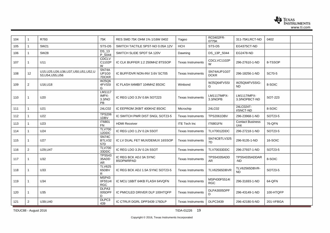
8.2 Bill of Materials
To download the Bill of Materials for each board, see the design files at http://www.ti.com/tool/TIDA-01226
Table 1: Bill of Material
Item Qty Reference Value Part Description Manufacturer Manufacturer Part Number
Alternate Part PCB Footprint
Note
1 47
C6,C49,C75,C190,C191,C225,C226,C227,C229,C233,C234,C236,C237,C238,C248,C250,C286,C287,C288,C308,C322,C326,C334,C346,C368,C369,C378,C379,C380,C381,C382,C383,C387,C388,C389,C390,C392,C393,C394,C395,C396,C397,C398,C420,C423,C424,C427
0.1uF 0.10µF ±10% 16V X7R Ceramic Capacitor
Yageo CC0402KRX7R7BB104
311-1338-1-ND 0402
2 75
C79,C89,C90,C91,C92,C93,C94,C95,C96,C97,C98,C99,C100,C101,C103,C104,C105,C106,C107,C108,C109,C110,C111,C112,C113,C114,C115,C116,C117,C118,C119,C120,C121,C122,C123,C124,C125,C126,C127,C128,C130,C131,C132,C146,C175,C176,C177,C178,C183,C186,C187,C188,C189,C194,C195,C196,C197,C198,C199,C202,C209,C211,C213,C215,C219,C220,C221,C222,C223,C224,C228,C276,C277,C278,C279
0.1uF 0.10µF ±10% 6.3V X5R Ceramic Capacitor
Yageo CC0201KRX5R5BB104
311-1408-1-ND 0201
3 3 C102,C129,C310 0.01uF 10000pF ±10% 25V X7R Ceramic Capacitor
Yageo CC0402KRX7R8BB103
311-1337-1-ND 0402
4 3 C179,C323,C412 10uF 10µF ±10% 25V X5R Ceramic Capacitor Yageo CC0805KKX5R8BB106
311-1869-1-ND 0805
5 15 C180,C181,C184,C193,C200,C206,C207,C208,C210,C212,C214,C218,C249,C273,C285
10uF 10µF ±20% 6.3V X5R Ceramic Capacitor Yageo CC0603MRX5R5BB106
311-1448-1-ND 0603
6 16 C182,C185,C192,C201,C203,C235,C245,C247,C274,C289,C320,C360,C367,C384,C386,C391
1uF 1µF ±10% 10V X5R Ceramic Capacitor Yageo CC0402KRX5R6BB105
311-1439-1-ND 0402
7 2 C216,C217 18pF 18pF ±5% 50V C0G, NP0 Ceramic Capacitor
Yageo CC0402JRNPO9BN180
311-1415-1-ND 0402
8 9 C230,C231,C232,C239,C240,C241,C2 0.1uF 0.10µF ±10% 25V X5R Ceramic Yageo CC0402KRX5R 311-1697-1-ND 0402

www.ti.com
TIDUC88 - August 2016 TIDA-01226 13
Copyright © 2016, Texas Instruments Incorporated
70,C417,C419 Capacitor 8BB104
9 2 C262,C410 0.1uF 0.10µF ±10% 50V X7R Ceramic Capacitor
Yageo CC0603KRX7R9BB104
311-1344-1-ND 0603
10 3 C263,C305,C324 10uF Multilayer Ceramic Capacitors MLCC - SMD/SMT 1206 10uF 50volt X5R +/-10%
Yageo CC1206KKX7R9BB106
GRM31CR61H106KA12L
1206
11 1 C264 220uF Aluminum Electrolytic Capacitors - SMD 50 Volts 220uF 20% 10x10.3
Lelon VZH221M1HTR-1010
140-VZH221M1HTR1010
EC-10
12 1 C266 120pF Multilayer Ceramic Capacitors MLCC - SMD/SMT 120pF 50V NPO 5%
Yageo CC0402JRNPO9BN121
603-CC402JRNPO9BN121
0402 (6 (c)); (7(c) I). Date: 03/31/16
13 5 C268,C271,C269,C416,C418 22uF 22µF ±10% 25V X5R Ceramic Capacitor Murata GRM32ER61E226KE15L
490-3889-1-ND 1210
14 4 C272,C300,C329,C333 10uF 10µF ±20% 10V X5R Ceramic Capacitor Yageo CC0603MRX5R6BB106
311-1817-1-ND 0603
15 1 C283 0.22uF 0.22µF ±10% 25V X7R Ceramic Capacitor
Yageo CC0603KRX7R8BB224
311-1803-1-ND 0603
16 10 C301,C302,C303,C304,C336,C337,C348,C349,C307,C313
22uF 22µF ±20% 35V X5R Ceramic Capacitor TDK C3216X5R1V226M160AC
445-8045-1-ND 1206
17 6 C306,C327,C328,C332,C312,C319 1uF 1µF ±10% 50V X5R Ceramic Capacitor Yageo CC0603KRX5R9BB105
311-1787-1-ND 0603
18 1 C309 1200pF 1200pF ±5% 50V C0G, NP0 Ceramic Capacitor
Yageo CC1206JRNPO9BN122
603-CC126JRNPO9BN122
1206 (6 (c)); (7(c) I). Date: 03/31/16
19 1 C311 15pF 15pF ±5% 50V C0G, NP0 Ceramic Capacitor
Yageo CC0402JRNPO9BN150
311-1017-1-ND 0402
20 1 C317 0.47uF 0.47µF ±10% 50V X5R Ceramic Capacitor
Yageo CC0603KRX7R9BB474
UMK107ABJ474KA-T
0603
21 1 C321 4300pF 4300pF ±5% 50V U2J Ceramic Capacitor Murata GRM1887U1H432JA01
490-6397-1-ND 0603
22 1 C330 2.2uF 2.2µF ±20% 6.3V X5R Ceramic Capacitor
Yageo CC0402MRX5R5BB225
311-1442-1-ND 0402
23 1 C331 4.7uF 4.7µF ±20% 6.3V X5R Ceramic Capacitor
Yageo CC0402MRX5R5BB475
311-1730-1-ND 0402
24 4 C340,C341,C353,C354 22uF 22µF ±20% 6.3V X5R Ceramic Capacitor Yageo CC0603MRX5R5BB226
311-1815-1-ND 0603
25 2 C342,C352 470pF 470pF ±10% 50V X7R Ceramic Capacitor
Yageo CC0603KRX7R9BB471
311-1078-1-ND 0603
26 2 C358,C363 1uF 1µF ±10% 25V X5R Ceramic Capacitor Yageo CC0402KRX5R8BB105
311-1698-1-ND 0402
27 1 C370 1000pF 1µF ±10% 25V X5R Ceramic Capacitor Yageo CC0603KRX7R9BB102
311-1080-1-ND 0603
28 1 C411 0.012uF 0.012µF ±10% 50V X7R Ceramic Yageo CC0603KRX7R 311-1807-1-ND 0603

www.ti.com
TIDUC88 - August 2016 TIDA-01226 14
Copyright © 2016, Texas Instruments Incorporated
Capacitor 9BB123
29 1 C413 22uF 22µF ±20% 10V X5R Ceramic Capacitor Yageo CC0805MKX5R6BB226
311-1900-1-ND 0805
30 2 C414,C415 4.7uF 4.7µF ±10% 25V X7R Ceramic Capacitor Yageo CC0805KKX7R8BB475
311-1885-1-ND 0805
31 1 C425 3300pF 3300pF ±10% 50V X7R Ceramic Capacitor
Yageo CC0402KRX7R9BB332
311-1034-1-ND 0402
32 36
ED1,ED2,ED3,ED4,ED5,ED6,ED7,ED8,ED9,ED10,ED11,ED12,ED13,ED14,ED15,ED16,ED19,D25,D26,ED21,ED22,ED17,ED18,ED20,ED23,ED24,ED25,ED26,ED27,ED36,ED37,ED38,ED39,ED40,ED41,ED42
PESD5V0U1BL.315
TVS DIODE 5VWM SOD882 NXP PESD5V0U1BL.315
568-4803-1-ND SOD882
33 1 D32 BAT54CW
DIODE ARRAY SCHOTTKY 30V SOT323
Diodes Inc. BAT54CW 568-1613-1-ND SOT323
34 11 D33,D34,D36,D44,D45,D46,D56,D57,D66,D67,D43
16-213SYGC/S530-E2/TR8
LED YELLOW-GRN CLEAR 0402 SMD Everlight 16-213SYGC/S530-E2/TR8
16-213SYGC/S530-E3/TR8-ND
0402
35 1 D51 MBR0540
DIODE SCHOTTKY 40V 500MA SOD123
ON Semi MBR0540 MBR0540T1GOSCT-ND
SOD123
36 3 D53,D54,D55 ESDA18-1K
TVS DIODE 15VWM 34VC SOD523 STMicroelectronics
ESDA18-1K 497-10767-1-ND SOD523
37 2 D58,D59 B0530WS-7
DIODE SCHOTTKY 30V 500MA SOD323
Diodes Inc. B0530WS-7 B0530WS-FDICT-ND
SOD323
38 2 D68,D69 SS0540 DIODE SCHOTTKY 40V 500MA SOD123
PANJIT SS0540 B0540W-FDICT-ND
SOD123
39 19 FB1,FB2,FB3,FB5,FB6,FB8,FB9,FB10,FB11,FB12,FB30,FB31,FB32,FB33,L5,L6,L7,L8,L9
GMLB-160808-0070S-N1
FERRITE BEAD 70 OHM 0603 1LN MAG.LAYERS GMLB-160808-0070S-N1
490-5253-1-ND 0603
40 6 FB20,FB22,FB23,FB24,FB25,FB26
GMLB-100505-0120P-N8
FERRITE BEAD 120 OHM 0402 1LN MAG.LAYERS GMLB-100505-0120P-N8
490-4004-1-ND 0402
41 1 J11 TU3007WNR-04
4 Positions Header, Shrouded Connector 0.098" (2.50mm) Through Hole, Right Angle Tin
TYU TU3007WNR-04 455-1627-ND
42 1 J18 47151-1101
HDMI Receptacle Connector 19 Position Surface Mount, Right Angle, Horizontal
Molex 47151-1101

www.ti.com
TIDUC88 - August 2016 TIDA-01226 15
Copyright © 2016, Texas Instruments Incorporated
43 1 J21 TU1501WNV-06
6 Positions Header, Shrouded Connector 0.059" (1.50mm) Through Hole Tin
TYU TU1501WNV-06 455-1661-ND
44 1 J22 104060-8017
CONN FFC FPC 80POS 0.50MM R/A Molex 104060-8017
45 1 J23 TU1501WNR-03S
3 Positions Header, Shrouded Connector 0.059" (1.50mm) Surface Mount, Right Angle Tin
TYU TU1501WNR-03S
455-1694-2-ND
46 4 J24,J43,J32,J33 TU1501WNV-03
3 Positions Header, Shrouded Connector 0.059" (1.50mm) Through Hole Tin
TYU TU1501WNV-03 455-1658-ND
47 1 J26 TU1252WNR-08S
8 Positions Header, Shrouded Connector 0.049" (1.25mm) Surface Mount, Right Angle Tin
TYU TU1252WNR-08S
WM7626TR-ND
48 1 J28 IDJ-D43B2
CON PWR JCK 2.5 X 6.0MM W/SHLD HCH IDJ-D43B2 CP-047BH-ND
49 1 J34 CH87142V200
14 Positions Header, Shrouded Connector 0.100" (2.54mm) Through Hole Gold
CviLux CH87142V200 WM6547-ND
50 1 J35 TU5005WNV-1x02
2 Positions Header, Unshrouded, Breakaway Connector 0.100" (2.54mm) Through Hole Tin
TYU TU5005WNV-1x02
WM8072-ND
51 3 J40,J41,J42 78048-1043
Headers & Wire Housings PCB HEADERS
Molex 78048-1043
52 1 J45 TU1252WNR-02S
2 Positions Header, Shrouded Connector 0.049" (1.25mm) Surface Mount, Right Angle Tin
TYU TU1252WNR-02S
WM7620TR-ND
53 1 J47 MU-05F4-24
USB - mini B USB 2.0 OTG Receptacle Connector 5 Position Surface Mount, Right Angle, Horizontal
OBJECTIVE MU-05F4-24 WM5461CT-ND

www.ti.com
TIDUC88 - August 2016 TIDA-01226 16
Copyright © 2016, Texas Instruments Incorporated
54 1 J48 TU2001WNV-06
6 Positions Header, Shrouded Connector 0.079" (2.00mm) Through Hole Tin
TYU TU2001WNV-06 455-1708-ND
55 1 L10 15uH FIXED IND 15UH 6.25A 45 MOHM SMD MAG.LAYERS MMD-10DZ-150M-M1
SRP1038A-150MCT-ND
56 1 L11 2.2uH Fixed Inductors XFL3012 Low DCR Ind 2.2 uH 20 % 1.9 A
MAG.LAYERS MLPS-3015-2R2 994-XFL3012-222MEC
57 1 L14 1.5uH FIXED IND 1.5UH 23A 3.16 MOHM MAG.LAYERS MMD-12EZ-1R5M-V1
283-4548-1-ND
58 1 L15 10uH FIXED IND 10UH 1.8A 243 MOHM SMD MAG.LAYERS MMD-04BZ-100M-S1
SRP4020TA-100MTR-ND
59 2 L16,L18 3.3uH FIXED IND 3.3UH 6A 30 MOHM SMD MAG.LAYERS MMD-06CZ-3R3M-V1
541-1009-1-ND
60 1 L21 CMM21T-900M-N
CMC 90 OHM 300MA 2 LN SMD Chilisin CMM21T-900M-N
445-5193-1-ND
61 2 Q4,Q7 2N7002P,215
MOSFET N-CH 60V 0.36A SOT-23 NXP 2N7002P,215
568-5818-1-ND SOT23
62 1 Q8 DMN26D0UT
MOSFET N-CH 20V 230MA SOT523 Diodes Inc. DMN26D0UT DMN26D0UT-7DICT-ND
SOT523
63 1 Q15 CSD17309Q3
MOSFET N-CH 30V 60A 8SON Texas Instruments CSD17309Q3 296-27250-1-ND 8SON
64 4 Q16,Q17,Q18,Q19 CSD17501Q5A
MOSFET N-CH 30V 100A 8SON Texas Instruments CSD17501Q5A 296-28437-1-ND 8SON
65 2 Q20,Q21 BCP68 TRANS NPN 20V 1A SOT223 NXP BCP68 568-6107-1-ND SOT223
66 2 Q22,Q23 MMBT2222ALT1G
TRANS NPN 40V 0.6A SOT23 ON Semi MMBT2222ALT1G
MMBT2222ALT1GOSCT-ND
SOT23
67 6 RP1,RP2,RP3,RP4,RP5,RP6 YC124-JR-0733R
RES ARRAY 4 RES 33 OHM 0804 Yageo YC124-JR-0733R
YC124J-33CT-ND 0402*4
68 45
R1,R2,R6,R139,R149,R162,R172,R173,R175,R176,R179,R209,R210,R349,R350,R351,R365,R367,R432,R433,R447,R612,R651,R652,R661,R662,R665,R666,R667,R668,R670,R671,R677,R679,R680,R685,R693,R699,R704,R706,R708,R769,R770,R795,R729
10K RES SMD 10K OHM 5% 1/16W 0402 Yageo RC0402JR-0710K
11-10KJRCT-ND 0402

www.ti.com
TIDUC88 - August 2016 TIDA-01226 17
Copyright © 2016, Texas Instruments Incorporated
69 119
R9,R109,R116,R120,R125,R140,R141,R171,R208,R211,R234,R235,R237,R239,R241,R242,R243,R356,R358,R359,R366,R368,R376,R377,R379,R387,R388,R389,R394,R395,R396,R397,R398,R399,R400,R402,R403,R404,R406,R408,R410,R411,R412,R413,R414,R415,R416,R417,R419,R425,R427,R430,R431,R435,R451,R452,R477,R478,R487,R488,R504,R505,R521,R525,R533,R534,R537,R538,R539,R540,R541,R542,R571,R579,R583,R604,R614,R615,R623,R629,R630,R631,R632,R636,R637,R638,R640,R641,R643,R644,R646,R650,R657,R659,R663,R664,R672,R673,R674,R676,R678,R682,R683,R684,R687,R688,R696,R702,R774,R775,R778,R779,R782,R798,R654,R655,R675,R619,R621
0 RES SMD 0.0OHM JUMPER 1/16W 0402
Yageo RC0402JR-070R
311-0.0JRCT-ND 0402
70 21 R12,R51,R52,R67,R68,R69,R71,R72,R73,R74,R75,R76,R121,R122,R123,R164,R182,R184,R186,R344,R584
30.1 RES SMD 30.1 OHM 1% 1/16W 0402 Yageo RC0402FR-0730R1
YAG3111CT-ND 0402
71 22
R35,R36,R37,R60,R63,R64,R65,R117,R118,R119,R142,R143,R169,R183,R185,R189,R345,R373,R393,R401,R436,R656
100K RES SMD 100K OHM 5% 1/16W 0402 Yageo RC0402JR-07100K
311-100KJRCT-ND
0402
72 2 R114,R115 43 RES SMD 43 OHM 5% 1/16W 0402 Yageo RC0402JR-0743R
311-43JRCT-ND 0402
73 6 R124,R126,R127,R136,R206,R207 7.5K RES SMD 7.5K OHM 1% 1/16W 0402 Yageo RC0402FR-077K5
311-7.50KLRCT-ND
0402
74 1 R348 300K RES SMD 300K OHM 1% 1/16W 0402 Yageo RC0402FR-07300K
311-300KLRCT-ND
0402
75 3 R352,R524,R474 47K RES SMD 47K OHM 5% 1/16W 0402 Yageo RC0402JR-0747K
311-47KJRCT-ND 0402
76 1 R355 2M RES SMD 2M OHM 5% 1/16W 0402 Yageo RC0402JR-072M
YAG3295CT-ND 0402
77 1 R357 22K RES SMD 22K OHM 1% 1/16W 0402 Yageo RC0402FR-0722K
311-22.0KLRCT-ND
0402
78 6 R360,R361,R363,R364,R362,R622 33 RES SMD 33 OHM 5% 1/16W 0402 Yageo RC0402JR-0733R
311-33JRCT-ND 0402
79 1 R375 4.75K RES SMD 4.75K OHM 1% 1/16W 0402 Yageo RC0402FR-074K75
311-4.75KLCT-ND 0402
80 2 R378,R785 1M RES SMD 1M OHM 1% 1/16W 0402 Yageo RC0402FR-071M
311-1.00MLRCT-ND
0402
81 1 R380 1.5K RES SMD 1.5K OHM 1% 1/16W 0402 Yageo RC0402FR-071K5
311-1.50KLRCT-ND
0402
www.ti.com
TIDUC88 - August 2016 TIDA-01226 18
Copyright © 2016, Texas Instruments Incorporated
82 1 R381 3K RES SMD 3K OHM 1% 1/16W 0402 Yageo RC0402FR-073K
311-3KLRCT-ND 0402
83 6 R383,R385,R613,R616,R689,R691 180 RES SMD 180 OHM 5% 1/16W 0402 Yageo RC0402JR-07180R
311-180JRCT-ND 0402
84 5 R437,R479,R526,R527,R528 390 RES SMD 390 OHM 5% 1/16W 0402 Yageo RC0402JR-07390R
311-390JRCT-ND 0402
85 1 R443 470K RES SMD 470K OHM 1% 1/16W 0402 Yageo RC0402FR-07470K
311-470KLRCT-ND
0402
86 5 R472,R575,R596,R600,R606 0 RES SMD 0.0 OHM JUMPER 1/4W 1206 Yageo RC1206JR-070R
311-0.0ERCT-ND 1206
87 2 R480,R471 215K RES SMD 215K OHM 1% 1/16W 0402 Yageo RC0402FR-07215K
YAG3055CT-ND 0402
88 1 R482 47.5K RES SMD 47.5K OHM 1% 1/16W 0402 Yageo RC0402FR-0747K5
311-47.5KLRCT-ND
0402
89 4 R529,R530,R635,R749 2.2K RES SMD 2.2K OHM 1% 1/16W 0402 Yageo RC0402FR-072K2
311-2.20KLRCT-ND
0402
90 2 R570,R572 3.9 RES SMD 3.9 OHM 5% 1/10W 0603 Yageo RC0603JR-073R9
311-3.9GRCT-ND 0603
91 1 R574 30K RES SMD 30K OHM 1% 1/16W 0402 Yageo RC0402FR-0730K
311-30.0KLRCT-ND
0402
92 1 R576 100K THERMISTOR NTC 100K OHM 1% 0402 THINKING TSM0A104F39H1RZ
490-4803-2-ND 0402
93 1 R578 3.9 Thick Film Resistors - SMD 3.9 OHM 5% Yageo RC1210JR-073R9
603-RC1210JR-073R9L
1210
94 2 R580,R582 10 RES SMD 10 OHM 1% 1/16W 0402 Yageo RC0402FR-0710R
311-10.0LRCT-ND 0402
95 3 R585,R586,R587 0 RES SMD 0.0OHM JUMPER 1/10W 0603
Yageo RC0603FR-070R
311-0.0HRCT-ND 0603
96 2 R591,R592 10K RES SMD 10K OHM 1% 1/16W 0402 Yageo RC0402FR-0710K
311-10.0KLRCT-ND
0402
97 1 R595 0.009 Current Sense Resistors - SMD 3watts .009ohms 1%
Ralec LR2512-23R009F4
71-WSLP25129L000FEA
2512 (7(c) I). Date: 05/01/16
98 2 R598,R602 10 RES SMD 10 OHM 1% 1/10W 0603 Yageo RC0603FR-0710R
311-10.0HRCT-ND
0603
99 1 R611 300 RES SMD 300 OHM 5% 1/16W 0402 Yageo RC0402JR-07300R
311-300JRCT-ND 0402
100 8 R743,R761,R762,R763,R765,R767,R768,R797
3.3K RES SMD 3.3K OHM 5% 1/16W 0402 Yageo RC0402JR-073K3
311-3.3KJRCT-ND 0402
101 1 R744 442 RES SMD 442 OHM 1% 1/10W 0603 Yageo RC0603FR-07442R
311-442HRCT-ND 0603
102 1 R745 140K RES SMD 140K OHM 1% 1/10W 0603 Yageo RC0603FR-07140K
311-140KHRCT-ND
0603
103 1 R747 30.9K RES SMD 30.9K OHM 1% 1/16W 0402 Yageo RC0402FR-0730K9
YAG3110CT-ND 0402
www.ti.com
TIDUC88 - August 2016 TIDA-01226 19
Copyright © 2016, Texas Instruments Incorporated
104 1 R793 75K RES SMD 75K OHM 1% 1/16W 0402 Yageo RC0402FR-0775K
311-75KLRCT-ND 0402
105 1 SW21 STS-D5 SWITCH TACTILE SPST-NO 0.05A 12V HCH STS-D5 EG4375CT-ND
106 1 SW28 DS_13P_S044
SWITCH SLIDE SPDT 5A 120V Dawning DS_13P_S044 EG2478-ND
107 1 U11 CDCLVC1102PW
IC CLK BUFFER 1:2 250MHZ 8TSSOP Texas Instruments CDCLVC1102PW
296-27610-1-ND 8-TSSOP
108 12 U15,U25,U26,U36,U37,U50,U51,U52,U53,U54,U55,U56
SN74AUP1G07DCKR
IC BUFF/DVR NON-INV 3.6V SC705 Texas Instruments SN74AUP1G07DCKR
296-18256-1-ND SC70-5
109 2 U16,U18 W25Q64FVSSIG
IC FLASH 64MBIT 104MHZ 8SOIC Winbond W25Q64FVSSIG
W25Q64FVSSIG-ND
8-SOIC
110 1 U20
LM1117IMPX-3.3/NOPB
IC REG LDO 3.3V 0.8A SOT223 Texas Instruments LM1117IMPX-3.3/NOPB
LM1117IMPX-3.3/NOPBCT-ND
SOT-223
111 1 U21 24LC02 IC EEPROM 2KBIT 400KHZ 8SOIC Microchip 24LC02 24LC024T-I/SNCT-ND
8-SOIC
112 1 U22 TPS2061DBV
IC SWITCH PWR DIST SNGL SOT23-5 Texas Instruments TPS2061DBV 296-23968-1-ND SOT23-5
113 1 U23 IT6801FN
HDMI Receiver ITE Tech Inc IT6801FN Contact Business Unit
76-QFN
114 1 U24 TLV70012DDC
IC REG LDO 1.2V 0.2A 5SOT Texas Instruments TLV70012DDC 296-27218-1-ND SOT23-5
115 1 U27 SN74CBTLV3257D
IC LV DUAL FET MUX/DEMUX 16SSOP Texas Instruments SN74CBTLV3257D
296-9135-1-ND 16-SOIC
116 2 U29,U47 TLV70033DDC
IC REG LDO 3.3V 0.2A 5SOT Texas Instruments TLV70033DDC 296-27937-1-ND SOT23-5
117 1 U32 TPS54335ADDAR
IC REG BCK ADJ 3A SYNC 8SOPWRPAD
Texas Instruments TPS54335ADDAR
TPS54335ADDAR-ND
8-SOIC
118 1 U33 TLV62565DBVR
IC REG BCK ADJ 1.5A SYNC SOT23-5 Texas Instruments TLV62565DBVR TLV62565DBVR-ND
SOT23-5
119 1 U34 MSP430F5514IRGC
IC MCU 16BIT 64KB FLASH 64VQFN Texas Instruments MSP430F5514IRGC
296-31693-1-ND 64-QFN
120 1 U35 DLPA3005DPFD
IC PMIC/LED DRIVER DLP 100HTQFP Texas Instruments DLPA3005DPFD
296-43149-1-ND 100-HTQFP
121 2 U39,U40 DLPC3439
IC CTRLR DGRL DPP3439 176DLP Texas Instruments DLPC3439 296-42180-5-ND 201-VFBGA

www.ti.com
TIDUC88 - August 2016 TIDA-01226 20
Copyright © 2016, Texas Instruments Incorporated
122 1 U44 TXS0102DCU
IC VOLT-LEVEL TRANSLATOR US8 Texas Instruments TXS0102DCU 296-21931-1-ND 8-VSSOP
123 2 U45,U46 SN74AVC4T774PWR
IC BUS TRANSCVR 4BIT DL 16TSSOP Texas Instruments SN74AVC4T774PWR
296-24739-1-ND 16-TSSOP
124 1 U48 CY7C65215-32LTXI
IC USB TO SERIAL BRIDGE 32QFN Cypress CY7C65215-32LTXI
CY7C65215-32LTXI-ND
32-QFN
125 1 U49 SN74LVC1G06DCK
IC INVERTER SINGLE 1INPUT SC705 Texas Instruments SN74LVC1G06DCK
296-8484-1-ND SC70-5
126 1 U62 LM2940IMP-5
IC REG LDO 5V 1A SOT223 Texas Instruments LAM2940IMP-5 LM2940IMP-5.0/NOPBCT-ND
SOT-223
127 1 U65 SN74LVC1G08DCK
IC GATE AND 1CH 2-INP SC-70-5 Texas Instruments SN74LVC1G08DCK
296-11602-1-ND SC70-5
128 1 X3 24MHz OSC XO 24.000MHZ CMOS SMD YOKE SO3225-024000-F1A-BBA-YA
535-13158-1-ND 3.2*2.5mm
129 1 Y1 27MHz 27MHz ±30ppm Crystal 18pF 50 Ohm YOKE S5032B-027000-FA-16-30-YA
887-1093-1-ND 5*3.2mm
130 0 C11,C12,C13,C14,C204,C205,C246,C275,C385
0.1uF 0.10µF ±10% 16V X7R Ceramic Capacitor
Yageo CC0402KRX7R7BB104
311-1338-1-ND 0402
131 0 C318,C325 0.33uF 0.33µF ±10% 6.3V X5R Ceramic Capacitor
Yageo CC0402KRX5R5BB334
311-1683-1-ND 0402
132 0 C426 33nF 0.033µF ±10% 16V X5R Ceramic Capacitor
Yageo CC0402KRX5R7BB333
311-1695-2-ND 0402
133 0 D50,D52 B240A-13-F
DIODE SCHOTTKY 40V 2A SMA Diodes Inc. B240A-13-F B240A-FDICT-ND DO-214AC, SMA
134 0 FB4,FB7
GMLB-160808-0070S-N1
FERRITE BEAD 70 OHM 0603 1LN MAG.LAYERS GMLB-160808-0070S-N1
490-5253-1-ND 0603
135 0 FB21
GMLB-100505-0120P-N8
FERRITE BEAD 120 OHM 0402 1LN MAG.LAYERS GMLB-100505-0120P-N8
490-4004-1-ND 0402
136 0 J20 TU5005WNV-1x02
2 Positions Header, Unshrouded, TYU TU5005WNV-1x02
WM8072-ND
137 0
R3,R4,R107,R108,R128,R129,R382,R384,R653,R669,R681,R694,R698,R707,R709,R790,R791,R792,R390,R374,R485,R486,R784,R617,R794,R353
10K RES SMD 10K OHM 5% 1/16W 0402 Yageo RC0402JR-0710K
11-10KJRCT-ND 0402

www.ti.com
TIDUC88 - August 2016 TIDA-01226 21
Copyright © 2016, Texas Instruments Incorporated
138 0
R131,R132,R145,R148,R150,R151,R177,R178,R197,R198,R220,R221,R240,R354,R386,R392,R409,R418,R481,R489,R535,R536,R610,R618,R620,R624,R639,R658,R660,R686,R690,R692,R701,R740,R757,R758,R759,R760,R764,R766,R771,R772,R780,R781,R799,R581,R609,R695,R697,R700,R703,R705,R776,R777,R796
0 RES SMD 0.0OHM JUMPER 1/16W 0402
Yageo RC0402JR-070R
311-0.0JRCT-ND 0402
139 0 R369,R370,R371,R372 100 RES SMD 100 OHM 5% 1/20W 0201 Yageo RC0201JR-07100R
311-100NCT-ND 0201
140 0 R407,R483,R788,R789 100K RES SMD 100K OHM 5% 1/16W 0402 Yageo RC0402JR-07100K
311-100KJRCT-ND
0402
141 0 R608,R750 0 RES SMD 0.0 OHM JUMPER 1/4W 1206 Yageo RC1206JR-070R
311-0.0ERCT-ND 1206
142 0 R783 330 RES SMD 330 OHM 5% 1/16W 0402 Yageo RC0402JR-07330R
311-330JRCT-ND 0402
143 0 U28,U63 SN74AUP1G07DCKR
IC BUFF/DVR NON-INV 3.6V SC705 Texas Instruments SN74AUP1G07DCKR
296-18256-1-ND SC70-5
144 0 R144 7.5K RES SMD 7.5K OHM 1% 1/16W 0402 Yageo RTT027501FTH 311-7.50KLRCT-ND
Ralec
145 0 C284 2.2nF 2200pF ±10% 16V X7R Ceramic Capacitor
Yageo CC0201KRX7R7BB222
311-1602-1-ND 0201
146 0 C314,C315 22uF 22µF ±20% 35V X5R Ceramic Capacitor TDK C3216X5R1V226M160AC
445-8045-1-ND 1206
147 0 J29,J30 TU5005WNV-1x03
3 Positions Header, Unshrouded TYU TU5005WNV-1x03
WM8073-ND
148 0 U64 TPS3808G01DRV
IC VOLT SUPERVISOR ADJ 6SON Texas Instruments TPS3808G01DRV
296-23656-1-ND 6-SON
www.ti.com
TIDUC88 - August 2016 TIDA-01226 22
Copyright © 2016, Texas Instruments Incorporated
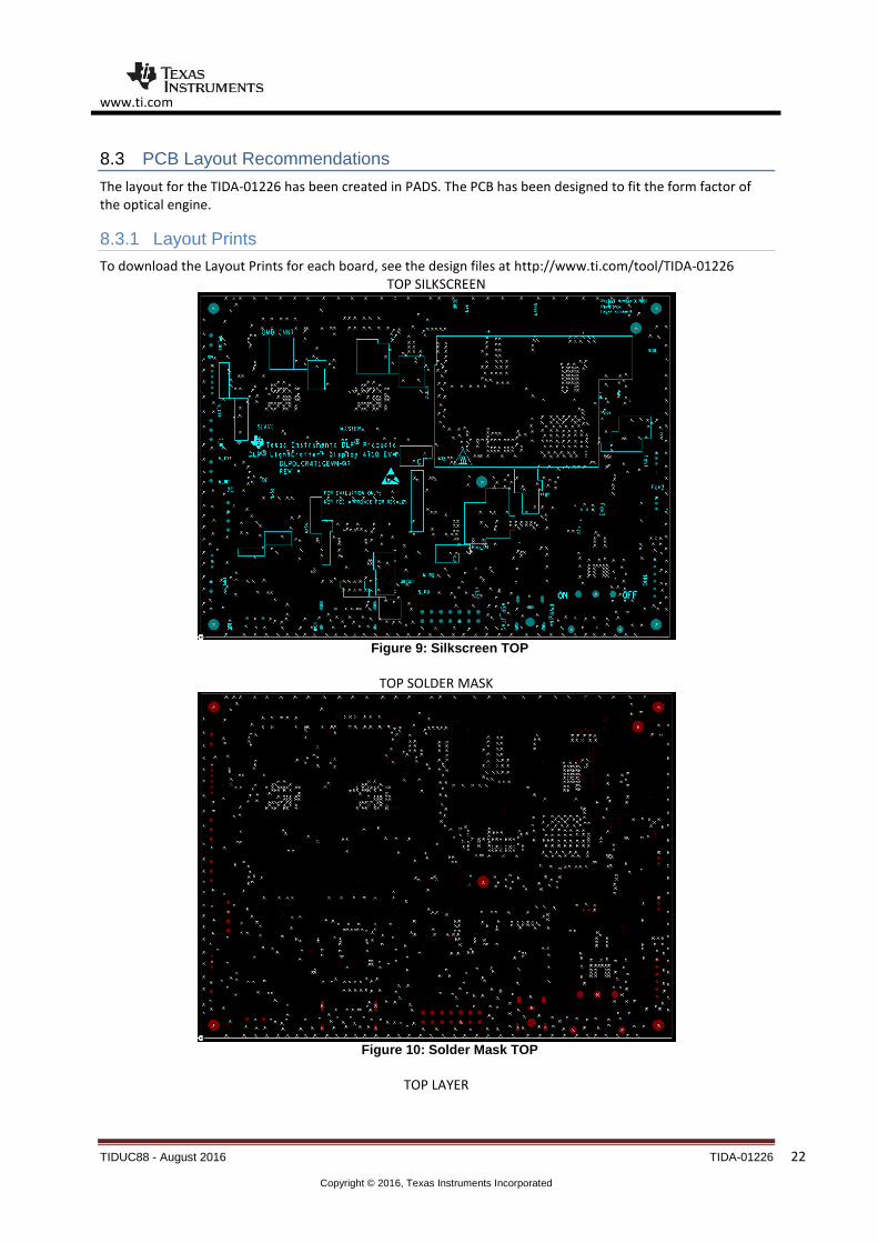
8.3 PCB Layout Recommendations
The layout for the TIDA-01226 has been created in PADS. The PCB has been designed to fit the form factor of the optical engine.
8.3.1 Layout Prints
To download the Layout Prints for each board, see the design files at http://www.ti.com/tool/TIDA-01226 TOP SILKSCREEN
Figure 9: Silkscreen TOP
TOP SOLDER MASK
Figure 10: Solder Mask TOP
TOP LAYER
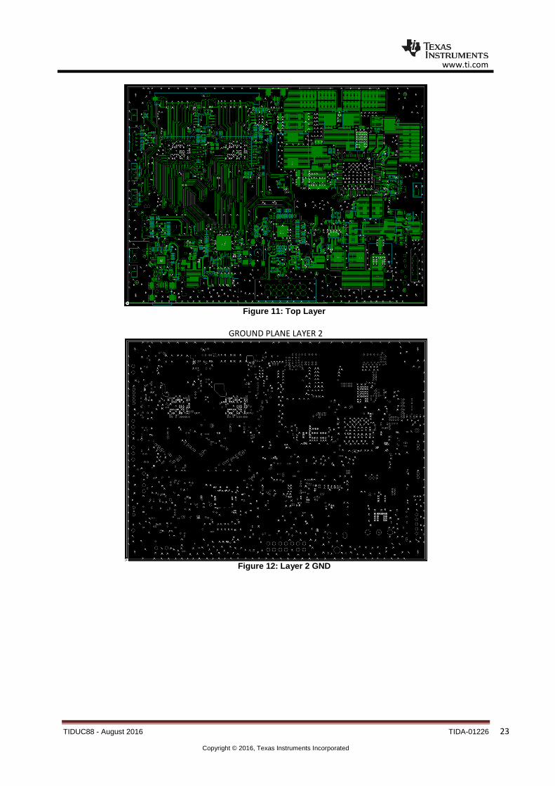
www.ti.com
TIDUC88 - August 2016 TIDA-01226 23
Copyright © 2016, Texas Instruments Incorporated
Figure 11: Top Layer
GROUND PLANE LAYER 2
Figure 12: Layer 2 GND
www.ti.com
TIDUC88 - August 2016 TIDA-01226 24
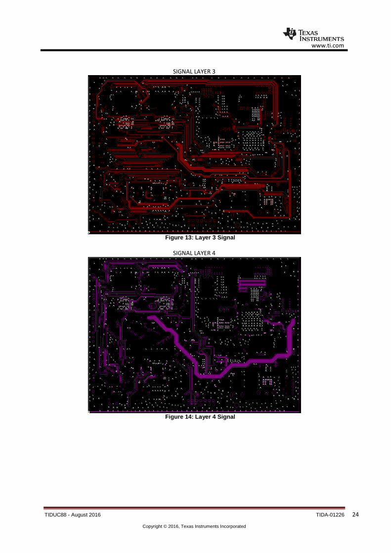
Copyright © 2016, Texas Instruments Incorporated
SIGNAL LAYER 3
Figure 13: Layer 3 Signal
SIGNAL LAYER 4
Figure 14: Layer 4 Signal

www.ti.com
TIDUC88 - August 2016 TIDA-01226 25
Copyright © 2016, Texas Instruments Incorporated
PWR LAYER 5
Figure 15: PWR Layer 5
BOTTOM LAYER
Figure 16: Bottom Layer
BOTTOM SOLDER MASK
www.ti.com
TIDUC88 - August 2016 TIDA-01226 26
Copyright © 2016, Texas Instruments Incorporated
Figure 17: Bottom Solder Mask
BOTTOM SILKSCREEN
Figure 18: Bottom Silkscreen

www.ti.com
TIDUC88 - August 2016 TIDA-01226 27
Copyright © 2016, Texas Instruments Incorporated
MECHANICAL DIMENSIONS
Figure 19: Mechanical Dimensions

www.ti.com
TIDUC88 - August 2016 TIDA-01226 28
Copyright © 2016, Texas Instruments Incorporated
8.4 PADS Project
The PADS project files for each board can be downloaded from http://www.ti.com/tool/TIDA-01226
Figure 20: Layout
www.ti.com
TIDUC88 - August 2016 TIDA-01226 29
Copyright © 2016, Texas Instruments Incorporated
8.5 Layout Guidelines
The layout guidelines shown here are subsets of the guidelines included in the component datasheets. Please also refer to the DLPC3439, DLP4710 and DLPA3005 datasheet for more information.
8.5.1 DLPC3439 Layout Guidelines
TI recommends 1-oz. copper planes in the PCB design to achieve needed thermal connectivity.
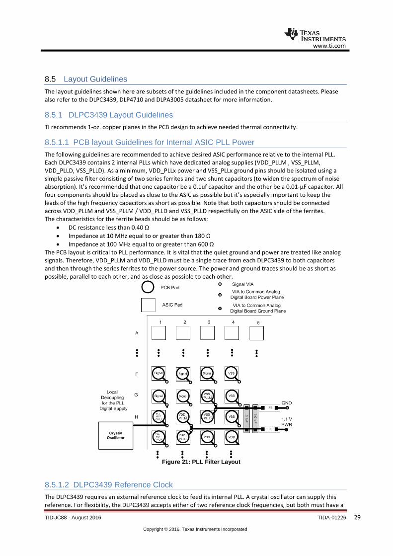
8.5.1.1 PCB layout Guidelines for Internal ASIC PLL Power
The following guidelines are recommended to achieve desired ASIC performance relative to the internal PLL. Each DLPC3439 contains 2 internal PLLs which have dedicated analog supplies (VDD_PLLM , VSS_PLLM, VDD_PLLD, VSS_PLLD). As a minimum, VDD_PLLx power and VSS_PLLx ground pins should be isolated using a simple passive filter consisting of two series ferrites and two shunt capacitors (to widen the spectrum of noise absorption). It’s recommended that one capacitor be a 0.1uf capacitor and the other be a 0.01-µF capacitor. All four components should be placed as close to the ASIC as possible but it’s especially important to keep the leads of the high frequency capacitors as short as possible. Note that both capacitors should be connected across VDD_PLLM and VSS_PLLM / VDD_PLLD and VSS_PLLD respectfully on the ASIC side of the ferrites. The characteristics for the ferrite beads should be as follows:
DC resistance less than 0.40 Ω
Impedance at 10 MHz equal to or greater than 180 Ω
Impedance at 100 MHz equal to or greater than 600 Ω The PCB layout is critical to PLL performance. It is vital that the quiet ground and power are treated like analog signals. Therefore, VDD_PLLM and VDD_PLLD must be a single trace from each DLPC3439 to both capacitors and then through the series ferrites to the power source. The power and ground traces should be as short as possible, parallel to each other, and as close as possible to each other.
Figure 21: PLL Filter Layout
8.5.1.2 DLPC3439 Reference Clock
The DLPC3439 requires an external reference clock to feed its internal PLL. A crystal oscillator can supply this reference. For flexibility, the DLPC3439 accepts either of two reference clock frequencies, but both must have a

www.ti.com
TIDUC88 - August 2016 TIDA-01226 30
Copyright © 2016, Texas Instruments Incorporated
maximum frequency variation of ±200 ppm (including aging, temperature, and trim component variation). The two DLPC3439 devices require a single dedicated oscillator where the oscillator output drives both DLPC3439 devices. The oscillator must drive the PLL_REFCLK_I pin on each DLPC3439 and the PLL_REFCLK_O pins should be left unconnected. The external oscillator must be able to drive at least a 15-pF load. Routing length from the oscillator to each DLPC3439 should be closely matched.
8.5.1.3 Number of Layer Changes
Single-ended signals: Minimize the number of layer changes
Differential signals: Individual differential pairs can be routed on different layers, but the signals of a given pair should not change layers.
8.5.1.4 Terminations
No external termination resistors are required on DMD_HS differential signals.
The DMD_LS_CLK and DMD_LS_WDATA signal paths should include a 43-Ω series termination resistor located as close as possible to the corresponding ASIC pins.
The DMD_LS_RDATA signal path should include a 43-Ω series termination resistor located as close as possible to the corresponding DMD pin.
DMD_DEN_ARSTZ does not require a series resistor.
Please refer to the DLPC3439 datasheet for length specifications.
8.5.1.5 Routing Vias and Stubs
There should be no more than two vias on any DMD_HS_signal.
Any and all vias on DMD_HS signals should be located as close to the ASIC as possible.
There should be now more than two vias on the DMD_LS_CLK and DMD_LS_WDATA signals.
Any and all vias on the DMD_LS_CLK and DMD_LS_WDATA signals should be located as close to the ASIC as possible.
Stubs should be avoided.
8.5.2 DLPA3005 Layout Guidelines
For switching power supplies, the layout is an important step in the design, especially when it concerns high peak currents and high switching frequencies. If the layout is not carefully done, the regulator could show stability issues and/or EMI problems. Therefore, it is recommended to use wide and short traces for high current paths and for their return power ground paths. For the DMD HV regulator, the input capacitor, output capacitor, and the inductor should be placed as close as possible to the IC. In order to minimize ground noise coupling between different buck converters it is advised to separate their grounds and connect them together at a central point under the part. For the DMD HV regulator, the recommended value for the capacitors is 1 µF for VRST and VOFS, 470 nF for VBIAS. The inductor value is 10 µH. The high currents of the buck converters concentrate around pins VIN, SWITCH and PGND (Figure 22). The voltage at the pins VIN, PGND and FB are DC voltages while the pin SWITCH has a switching voltage between VIN and PGND. When the FET betweenpins 52 – 53 is closed the red line indicates the current flow while the blue line indicates the current flow when the FET between pins 53 – 54 is closed. These paths carry the highest currents and must be kept as short as possible. For the LDO supply to the DMD, it is recommended to use a 1 µF/16 V capacitor on the input and a 10 µF/6.3 V capacitor on the output of the LDO assuming an input voltage of 12 V. For LDO bucks, it is recommended to use a 1 µF/16 V capacitor on the input and a 1 µF/6.3 V capacitor on the output of the LDO.

www.ti.com
TIDUC88 - August 2016 TIDA-01226 31
Copyright © 2016, Texas Instruments Incorporated
Figure 22: High AC Current Paths in a Buck Converter
The trace to the VIN pin carries high AC currents. Therefore the trace should have the lowest possible resistance to prevent voltage drop across the trace. Additionally the decoupling capacitors should be placed as close to the VIN pin as possible. The SWITCH pin is connected back and forth between the VIN or GND. This means a square wave voltage is present on the SWITCH pin with amplitude of VIN, and containing high frequencies. This can lead to EMI problems if not properly handled. To reduce EMI problems a snubber network (RSN7 & CSN7) is placed at the SWITCH pin to prevent and/or suppress unwanted high frequency ringing at the moment of switching. The PGND pin sinks high current and should also be connected to a star ground point such that it does not interfere with other ground connections. The FB pin is the sense connection for the regulated output voltage which is a DC voltage; no current is flowing through this pin. The voltage on the FB pin is compared with the internal reference voltage in order to control the loop. The FB connection should be made at the load such that I•R drop is not affecting the sensed voltage.
8.5.2.1 SPI Connections
The SPI interface consists of several digital lines and the SPI supply. If routing of the interface lines is not done properly, communication errors can occur. The SPI lines should not be routed close to potential interfering sources. Noise cntamination can be prevented by ensuring that the SPI ground line is routed together with the digital lines as much as possible to the respective pins. The SPI interface should have a dedicated ground connection to the DGND of the DLPA3005 (Figure 23). This prevents ground noise between SPI ground references of DLPA3005 and DLPC due to the high current in the system.

www.ti.com
TIDUC88 - August 2016 TIDA-01226 32
Copyright © 2016, Texas Instruments Incorporated
Figure 23: SPI Connections
Interfering sources should be kept away from the interface lines as much as possible. Especially high current lines such as neighboring PWR_7 should be routed carefully. If PWR_7 is routed too close to for instance the SPI_CLK it could lead to false clock pulses and thus communication errors.
8.5.2.2 RLIM Routing
RLIM is used to sense the LED current. To accurately measure the LED current, the RLIM _K_1,2 lines should be connected close to the top-side of measurement resistor RLIM, while RLIM_BOT_K_1,2 should be connected close to the bottom-side of RLIM. The switched LED current is running through RLIM. Therefore a low-ohmic ground connection for RLIM is strongly advised.
8.5.2.3 LED Connection
The wiring from the external RGB switches to the LEDs carries large switching currents. Special attention needs to be paid to these connections. Two perspectives apply to the LED-to-RGB switches wiring:
1. The resistance of the wiring, Rseries 2. The inductance of the wiring, Lseries
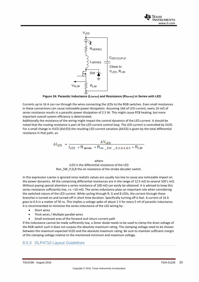
The location of the parasitic series impedances are depicted in Figure 24.
www.ti.com
TIDUC88 - August 2016 TIDA-01226 33
Copyright © 2016, Texas Instruments Incorporated
Figure 24: Parasitic Inductance (LSeries) and Resistance (RSeries) in Series with LED
Currents up to 16 A can run through the wires connecting the LEDs to the RGB switches. Even small resistances in these connections can cause noticeable power dissipation. Assuming 16A of LED current, every 10 mΩ of series resistance results in a parasitic power dissipation of 2.5 W. This might cause PCB heating, but more important overall system efficiency is deteriorated. Additionally the resistance of the wiring might impact the control dynamics of the LED current. It should be noted that the routing resistance is part of the LED current control loop. The LED current is controlled by VLED. For a small change in VLED (ΔVLED) the resulting LED current variation (ΔILED) is given by the total differential resistance in that path, as:
where rLED is the differential resistance of the LED
Ron_SW_P,Q,R the on resistance of the strobe decoder switch.
In this expression Lseries is ignored since realistic values are usually too low to cause any noticeable impact on the power dynamics. All the comprising differential resistances are in the range of 12.5 mΩ to several 100’s mΩ. Without paying special attention a series resistance of 100 mΩ can easily be obtained. It is advised to keep this series resistance sufficiently low, i.e. <10 mΩ. The series inductance plays an important role when considering the switched nature of the LED current. While cycling through R, G and B LEDs, the current through these branches is turned-on and turned-off in short time duration. Specifically turning off is fast. A current of 16 A goes to 0 A in a matter of 50 ns. This implies a voltage spike of about 1 V for every 5 nH of parasitic inductance. It is recommended to minimize the series inductance of the LED wiring by:
Short wires
Thick wires / Multiple parallel wires
Small enclosed area of the forward and return current path If the inductance cannot be made sufficiently low, a Zener diode needs to be used to clamp the drain voltage of the RGB switch such it does not surpass the absolute maximum rating. The clamping voltage need to be chosen between the maximum expected VLED and the absolute maximum rating. Be sure to maintain sufficient margin of the clamping voltage relative to the mentioned minimum and maximum voltage.
8.5.3 DLP4710 Layout Guidelines
www.ti.com
TIDUC88 - August 2016 TIDA-01226 34
Copyright © 2016, Texas Instruments Incorporated
There are no specific layout guidelines for the DMD as the DMD is typically connected using a board to board connector to and a flex cable. The flex cable provides the interface of data and ctrl signals between the DLPC3439 controller and the DLP4710 DMD. Some layout guideline for the flex cable interface to the DMD are:
Match lengths for the LS_WDATA and LS_CLK signals.
Minimize vias, layer changes, and turns for the HS bus signals.
Minimum of two 220-nF decoupling capacitor close to VBIAS.
Minimum of two 220-nF decoupling capacitor close to VRST.
Minimum of two 220-nF decoupling capacitor close to VOFS.
Minimum of four 220-nF decoupling capacitor close to VDDI and VDD.

www.ti.com
TIDUC88 - August 2016 TIDA-01226 35
Copyright © 2016, Texas Instruments Incorporated
8.6 Gerber files
To download the Gerber files for each board, see the design files at http://www.ti.com/tool/TIDA-01226
Figure 25: Gerber Layer 1

www.ti.com
TIDUC88 - August 2016 TIDA-01226 36
Copyright © 2016, Texas Instruments Incorporated
8.7 Assembly Drawings
To download the Assembly Drawings for each board, see the design files at http://www.ti.com/tool/TIDA-01226
Figure 26: Assembly TOP

www.ti.com
TIDUC88 - August 2016 TIDA-01226 37
Copyright © 2016, Texas Instruments Incorporated
9 Software Files To download the software files for this reference design, please see the link at http://www.ti.com/tool/DLPDLCR4710EVM-G2
10 References
1. Texas Instruments E2E Community, https://e2e.ti.com/support/dlp__mems_micro-electro-mechanical_systems
2. Texas Instruments DLPC3439 datasheet http://www.ti.com/lit/ds/symlink/dlpc3439.pdf 3. Texas Instruments DLPA3005 datasheet http://www.ti.com/lit/ds/symlink/dlpa3005.pdf 4. Texas Instruments DLP4710 datasheet http://www.ti.com/lit/ds/symlink/dlp4710.pdf

IMPORTANT NOTICE FOR TI REFERENCE DESIGNS
Texas Instruments Incorporated (‘TI”) reference designs are solely intended to assist designers (“Designer(s)”) who are developing systemsthat incorporate TI products. TI has not conducted any testing other than that specifically described in the published documentation for aparticular reference design.TI’s provision of reference designs and any other technical, applications or design advice, quality characterization, reliability data or otherinformation or services does not expand or otherwise alter TI’s applicable published warranties or warranty disclaimers for TI products, andno additional obligations or liabilities arise from TI providing such reference designs or other items.TI reserves the right to make corrections, enhancements, improvements and other changes to its reference designs and other items.Designer understands and agrees that Designer remains responsible for using its independent analysis, evaluation and judgment indesigning Designer’s systems and products, and has full and exclusive responsibility to assure the safety of its products and compliance ofits products (and of all TI products used in or for such Designer’s products) with all applicable regulations, laws and other applicablerequirements. Designer represents that, with respect to its applications, it has all the necessary expertise to create and implementsafeguards that (1) anticipate dangerous consequences of failures, (2) monitor failures and their consequences, and (3) lessen thelikelihood of failures that might cause harm and take appropriate actions. Designer agrees that prior to using or distributing any systemsthat include TI products, Designer will thoroughly test such systems and the functionality of such TI products as used in such systems.Designer may not use any TI products in life-critical medical equipment unless authorized officers of the parties have executed a specialcontract specifically governing such use. Life-critical medical equipment is medical equipment where failure of such equipment would causeserious bodily injury or death (e.g., life support, pacemakers, defibrillators, heart pumps, neurostimulators, and implantables). Suchequipment includes, without limitation, all medical devices identified by the U.S. Food and Drug Administration as Class III devices andequivalent classifications outside the U.S.Designers are authorized to use, copy and modify any individual TI reference design only in connection with the development of endproducts that include the TI product(s) identified in that reference design. HOWEVER, NO OTHER LICENSE, EXPRESS OR IMPLIED, BYESTOPPEL OR OTHERWISE TO ANY OTHER TI INTELLECTUAL PROPERTY RIGHT, AND NO LICENSE TO ANY TECHNOLOGY ORINTELLECTUAL PROPERTY RIGHT OF TI OR ANY THIRD PARTY IS GRANTED HEREIN, including but not limited to any patent right,copyright, mask work right, or other intellectual property right relating to any combination, machine, or process in which TI products orservices are used. Information published by TI regarding third-party products or services does not constitute a license to use such productsor services, or a warranty or endorsement thereof. Use of the reference design or other items described above may require a license from athird party under the patents or other intellectual property of the third party, or a license from TI under the patents or other intellectualproperty of TI.TI REFERENCE DESIGNS AND OTHER ITEMS DESCRIBED ABOVE ARE PROVIDED “AS IS” AND WITH ALL FAULTS. TI DISCLAIMSALL OTHER WARRANTIES OR REPRESENTATIONS, EXPRESS OR IMPLIED, REGARDING THE REFERENCE DESIGNS OR USE OFTHE REFERENCE DESIGNS, INCLUDING BUT NOT LIMITED TO ACCURACY OR COMPLETENESS, TITLE, ANY EPIDEMIC FAILUREWARRANTY AND ANY IMPLIED WARRANTIES OF MERCHANTABILITY, FITNESS FOR A PARTICULAR PURPOSE, AND NON-INFRINGEMENT OF ANY THIRD PARTY INTELLECTUAL PROPERTY RIGHTS.TI SHALL NOT BE LIABLE FOR AND SHALL NOT DEFEND OR INDEMNIFY DESIGNERS AGAINST ANY CLAIM, INCLUDING BUT NOTLIMITED TO ANY INFRINGEMENT CLAIM THAT RELATES TO OR IS BASED ON ANY COMBINATION OF PRODUCTS ASDESCRIBED IN A TI REFERENCE DESIGN OR OTHERWISE. IN NO EVENT SHALL TI BE LIABLE FOR ANY ACTUAL, DIRECT,SPECIAL, COLLATERAL, INDIRECT, PUNITIVE, INCIDENTAL, CONSEQUENTIAL OR EXEMPLARY DAMAGES IN CONNECTION WITHOR ARISING OUT OF THE REFERENCE DESIGNS OR USE OF THE REFERENCE DESIGNS, AND REGARDLESS OF WHETHER TIHAS BEEN ADVISED OF THE POSSIBILITY OF SUCH DAMAGES.TI’s standard terms of sale for semiconductor products (http://www.ti.com/sc/docs/stdterms.htm) apply to the sale of packaged integratedcircuit products. Additional terms may apply to the use or sale of other types of TI products and services.Designer will fully indemnify TI and its representatives against any damages, costs, losses, and/or liabilities arising out of Designer’s non-compliance with the terms and provisions of this Notice.IMPORTANT NOTICE
Mailing Address: Texas Instruments, Post Office Box 655303, Dallas, Texas 75265Copyright © 2016, Texas Instruments Incorporated