timing analysis - sisoft timing-ver09.pdf · this paper highlights timing analysis as one of ......
TRANSCRIPT

1 | P a g e
TIMING ANALYSIS
CONCEPT TO PRACTICE
IN
SIGNAL INTEGRITY

2 | P a g e
ABSTRACT:
This paper highlights timing analysis as one of the key issues that must be incorporated into the design methodology for engineers performing pre-layout solution space analysis to identify topology and termination schemes or post layout verification to validate physical implementation of designs.
This white-paper is targeted for engineers practicing in the area of signal integrity using the Quantum-SI tool or engineers and engineering students who are learning timing analysis methodologies as part of their signal integrity training. The reader is assumed to be familiar with waveform propagation over interconnects and signal integrity terminology, such as interconnect delays, flight-times, reflections, crosstalk, etc. It is also assumed that readers are familiar with component output/input timing parameters, like clock-to-data-valid, setup and hold times, as well as clock-related parameters, like jitter and skew.
AUTHOR BIOGRAPHY: Haluk Katircioglu is a lecturer in the Computer Engineering Department, School of Engineering, San Jose State University. He teaches graduate courses including the High-Speed Digital System Design course, as well as undergraduate courses within the department. He has extensive experience from silicon design to platform design and signal integrity working at Intel corporation. Peter LaFlamme, applications engineer, SiSoft Inc.
Shilpa Srinivasan is a graduate student specilizing in system design, graduating in May 2017. She has systems engineering experience from Tata Consultancy Services Ltd.
ACKNOWLEDGEMENTS:
Sisoft Inc. for the donation of the QSI software to the Computer Engineering Department for use in the High-Speed Digital System Design Course. Steve Silva, SiSoft Inc. for reviewing and commenting on the paper. TRADEMARKS:
SiSoft, Quantum-SI,TransferNet, are trademarks of Signal Integrity Software, Inc.

3 | P a g e
INTRODUCTION With the advent of high-speed digital design, signal integrity has become a critical issue, resulting in increasing challenges to the design engineers. As data communication speeds increase beyond 10 Gbps, designing for optimal signal integrity becomes a mandate to ensure reliable data. In high speed board/package design, designers are trying to eliminate or minimize all the impedance mismatches along the high speed signal path. Although the main focus of Signal Integrity is on both quality and timing of signals, the timing parameters pose special constraints on the circuits and interconnects at very high speeds (allowing sufficient setup and hold time at the receiver and also considering the clocking techniques used). While simulation tools have also gone through extensive development phases in the industry in order to meet the higher accuracy challenge in analysis at higher speeds, timing analysis methods, specifically, seem to differ among the commercially available software tools. This white-paper is only a review of the timing analysis methodology used in the Quantum-SITM tool. It includes review of waveform quality, slew rate, timing parameters and interconnect delay data for every edge of every waveform, as well as providing details on entering timing parameters so as to enable timing margin calculations in the tool. For a complete description of the design simulation methodology, readers should refer to the QSI documents. The organization of the paper is as follows: First, an introduction is presented on the timing analysis concept. This is followed by in depth descriptions of common-clock and source synchronous interfaces and the QSI methodology for validating the timing of these interfaces. It is recommended that the reader use the documents listed below as a reference while reading the paper: QSI_Users_Guide from SiSoft.com – for information on how to use the tool and timing files
QSI_Tutorials from SiSoft.com – for information on how to use the tool and timing files
DDR2 Design Kits, Signal Integrity Software, Inc. – for specific examples on memory interface simulations and timing analysis
Features and Implementation of High-performance 667Mbs and 800Mbs DDRII Memory Systems, DesignCon2005, Dail Robert Cox, Micron Technology, Inc. Randy Wolff, Micron Technology, Inc.; Doug Burns, Signal Integrity Software, Inc.; Barry Katz, Signal Integrity Software, Inc. Walter Katz, Signal Integrity Software, Inc. – for detailed information on memory interface simulations
JESD79F, JESD79-2F, JESD79-3F, JESD79-4A DDRx SDRAM SPECIFICATIONs – for DDR interface industry standards
DDR, DDR2, DDR3, DDR4 datasheets, Micron Technology, Inc – for information on memory device parameters
4 | P a g e
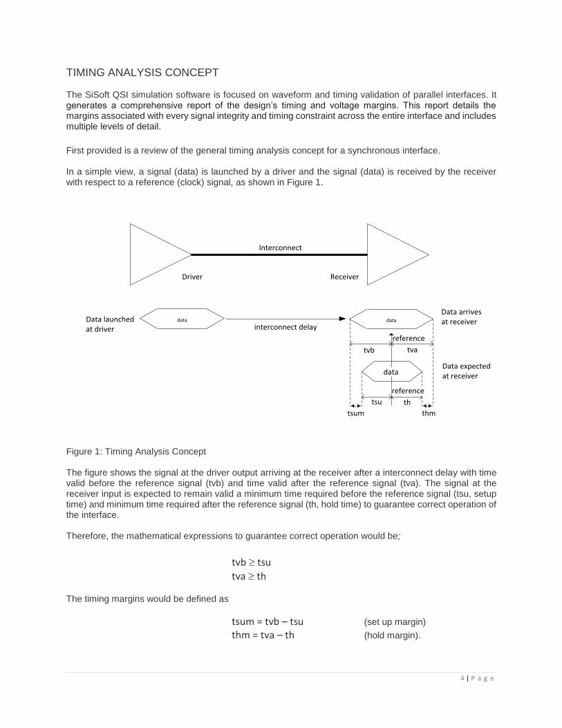
TIMING ANALYSIS CONCEPT The SiSoft QSI simulation software is focused on waveform and timing validation of parallel interfaces. It generates a comprehensive report of the design’s timing and voltage margins. This report details the margins associated with every signal integrity and timing constraint across the entire interface and includes multiple levels of detail.
First provided is a review of the general timing analysis concept for a synchronous interface. In a simple view, a signal (data) is launched by a driver and the signal (data) is received by the receiver with respect to a reference (clock) signal, as shown in Figure 1.
Figure 1: Timing Analysis Concept The figure shows the signal at the driver output arriving at the receiver after a interconnect delay with time valid before the reference signal (tvb) and time valid after the reference signal (tva). The signal at the receiver input is expected to remain valid a minimum time required before the reference signal (tsu, setup time) and minimum time required after the reference signal (th, hold time) to guarantee correct operation of the interface. Therefore, the mathematical expressions to guarantee correct operation would be;
tvb tsu
tva th The timing margins would be defined as
tsum = tvb – tsu (set up margin) thm = tva – th (hold margin).
Driver Receiver
data
interconnect delay
Interconnect
tvb tva
data
tsu th
data
tsum thm
reference
Data launched at driver
Data arrives at receiver
Data expected at receiver
reference

5 | P a g e
The signal at the driver is launched with known timing parameters (from the data sheet of the component) with respect to a reference signal (for example: clock signal). Normally the same reference signal is used at the driver and the receiver. Calculations of the valid-before and valid-after times at the receiver could be performed and derived through modeling of the IO buffers and simulations to determine the propagation delay across the interconnect.
The types of interfaces will be discussed to further the details of computation of timing margins with respect to the reference signals used in the interfaces. At the lower part of the timing diagrams describing interfaces, margin equations are shown for calculations using the datasheet parameters. The QSI equations with translated parameters are given within the text explaining the diagrams. The synchronous interface first described here is referred to as a common clock interface.
COMMON-CLOCK INTERFACE Synchronous interfaces in early systems, were common-clock, like PCI, PCIx and SDR memory. SDR (single-data rate) SDRAMs, though earlier memory technology but still used in systems today, are designed with a reference signal supplied to both the driver and the receiver from the same source. Such a design is commonly referred to as a common-clock interface and is described in Figure 2. Figure 2: Common-clock Interface Concept The driver sends the data signal with respect to the clock, named clkD, and the receiver receives the data signal with the clock clkR. The timing parameters of the data with respect to the clock at the driver and the receiver are provided in the respective data sheets. The simulation software tools would determine the propagation delays on all the interconnects. Timing margins of the data signal are affected by the clock skew which is defined as the difference between the arrival times of the clock signal at the driver and receiver inputs. The clock skew is calculated from the clkD and clkR propagation delays plus the skew between the outputs of the clock source and the jitter that the clock source may have.
A COMMON-CLOCK INTERFACE EXAMPLE: Setup skew timing and hold skew timing are shown in the timing diagrams in Figure 3 and Figure 4, respectively. Therefore, the margin equations can be written as
Driver Receiver
data interconnect
clock buffer
clkD clkRclkD interconnect clkR interconnect
clkSkew@buffer
clock skew

6 | P a g e
tsum = tCYC – tCOmax – tfltDmax – tsu – tsetupskew thm = tCOmin _ tfltDmin – th - tholdskew The margins, tsum and thm are computed by QSI based on the tflDmax and tfltDmin determined as a result of the simulations. tCYC, tCOmax, tCOmin, tsu, th and tjitter are parameters that are obtained from the datasheets and need to be entered into the QSI tool so the margins can be calculated. In QSI, UI = tCYC as shown in the Transfer Net of the Data signal Max Tco = tCOmax Max Data Etch Delay = tfltDmax Setup = tsu setup skew = (-) tsetupskew Min Tco = tCOmin Min Data Etch Delay = tfltDmin Hold = th hold skew = (+) tholdskew jitter = tjitter The equations used for margin calculations in QSI are: setup margin = UI - Max Tco - Max Data Etch Delay + Setup Skew - Setup hold margin = Min Tco + Min Data Etch Delay - Hold Skew - Hold setup skew = Clock Skew Min + Min Target Clock Etch Delay - Max Source Clock Etch Delay - Jitter hold skew = Clock Skew Max + Max Target Clock Etch Delay - Min Source Clock Etch Delay Setup Skew is the clock skew condition that creates the worst case setup margin and is equal to the difference between the latest source (driver) clock and the earliest target (receiver) clock. If the value is negative as shown in the timing diagram, it reduces setup margin. Hold Skew is the clock skew condition that creates the worst case hold margin and is equal to the difference between the earliest source (driver) clock and latest target (receiver) clock. If the value of the skew is positive as shown in the timing diagram, it reduces hold margin. TCO, clock-to-output parameter for the data signal needs to be entered in the driver timing file (.tmg file) as follows: DELAY R CLK *TO DATA MIN_TCO MAX_TCO MIN_TCO MAX_TCO with syntax DELAY <Edge> <Clock Timing Group> *TO <Data Timing Group> <Tco Min> <Tco Max> Similarly setup and hold times should be entered in the receiver timing file: SETHLD DATA *TO R CLK SETUP HOLD with syntax SETHLD <Data Timing Group> *TO <Edge> <Clock Timing Group> <Setup Time> <Hold Time> For other forms of the DELAY statement, QSI User Manual should be referred to. The clock skew also needs to be included in the calculations, therefore needs to be provided to the simulation tool, in this case QSI.

7 | P a g e
Figure 3: Timing Diagram for a common-clock interface - setup margin
tsutsum thmth
clkD@driver
tclkD
interconnect
delay min
(Min Source
Clock
Etch Delay )
tCOmax
data@driver
data@receiver
tfltDmin
(Min Data
Etch Delay )
tfltDmax
(Max Data
Etch Delay )
clkD@buffer
tCYC
tclkD
interconnect
delay max
(Max Source Clock
Etch Delay)
clkR@buffer
clkR@receiver
tclkSkewMin@buffer
early clock
tclkSkewMax@buffer
tCOmin
setup skew
tCYC = tCOmax + tfltDmax +tsu + tsum +tsetupskew
tCOmax
reference
clock
tclkR
interconnect
delay min
(Min Target
Clock Etch
Delay)
tclkR
interconnect
delay max
(Max Target Clock
Etch Delay )
setupmargin
holdskew
tsetupskew = tclkSkewMin@buffer + tclkR interconnect delay min – tclkD interconnect delay max – tjitter
tsum = tCYC - tCOmax - tfltDmax - tsetupskew - tsu
late clock
tCOmin
tfltDmin
(Min Data
Etch Delay )
tfltDmax
(Max Data
Etch Delay )
BLACK line arrows and labels: Data sheet parameters or calculated or simulated parameters
RED line arrows and labels: QSI parameters – used in .tmg files – translated from data-sheet parameters
BLUE line arrows and labels: Delays determined by QSI simulations
GREEN line arrows and labels: (r) rising edge, (f) falling or () both rising and falling edge setup, hold margin
Dashed lines point to labels
Faded color line arrows and labels are those not considered for calculations described in this figure
Max TCO
setup
tjitter
jitter
tjitter
jitter
Clock Skew Min
jitterjitter
tjitter
tsetupskew
8 | P a g e
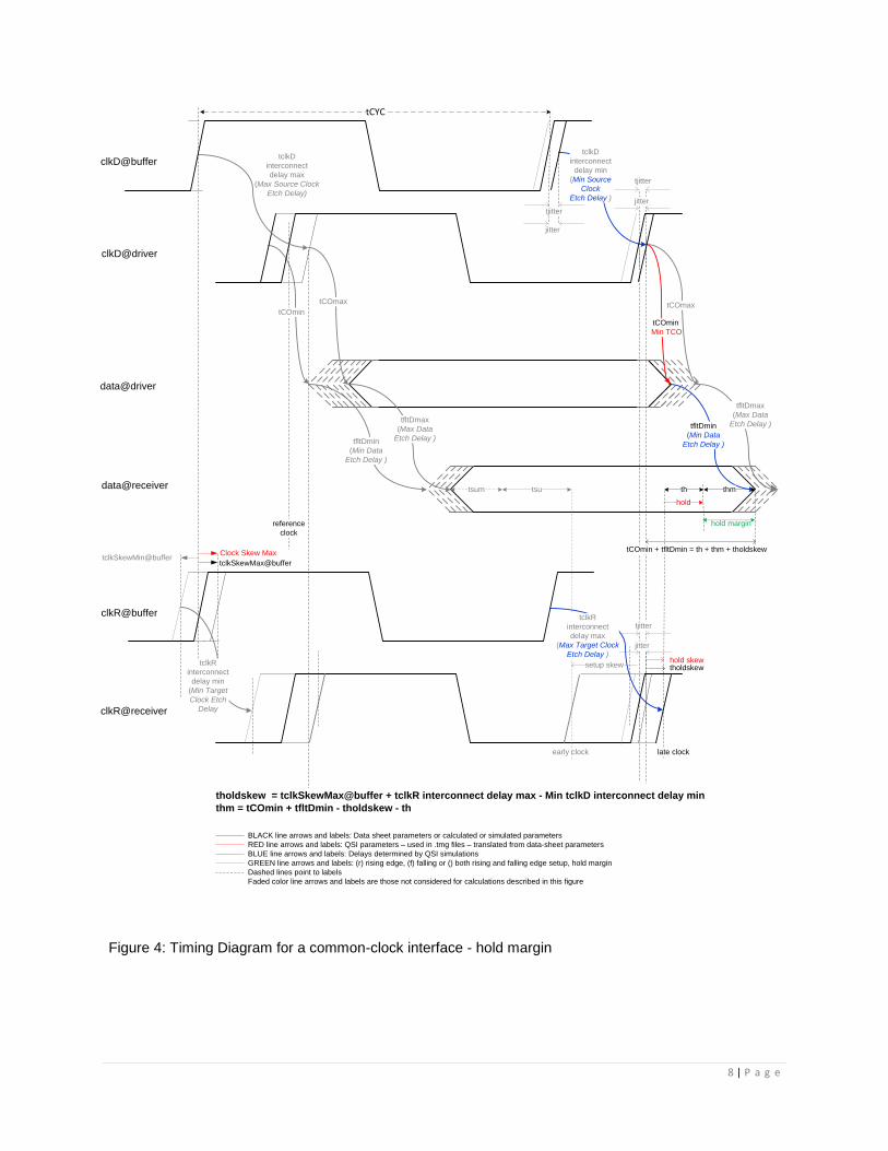
Figure 4: Timing Diagram for a common-clock interface - hold margin
thmth
clkD@driver
tclkD
interconnect
delay min
(Min Source
Clock
Etch Delay )
tCOmax
data@driver
data@receiver
tfltDmin
(Min Data
Etch Delay )
tfltDmax
(Max Data
Etch Delay )
clkD@buffer
tCYC
tclkD
interconnect
delay max
(Max Source Clock
Etch Delay)
clkR@buffer
clkR@receiver
tclkSkewMin@buffer
early clock late clock
tclkSkewMax@buffer
tCOmin
tCOmax
reference
clock
tclkR
interconnect
delay min
(Min Target
Clock Etch
Delay
hold margin
hold skew
tholdskew = tclkSkewMax@buffer + tclkR interconnect delay max - Min tclkD interconnect delay min
thm = tCOmin + tfltDmin - tholdskew - th
tCOmin + tfltDmin = th + thm + tholdskew
tfltDmax
(Max Data
Etch Delay )tfltDmin
(Min Data
Etch Delay )
tCOmin
tsutsum
setup skew
BLACK line arrows and labels: Data sheet parameters or calculated or simulated parameters
RED line arrows and labels: QSI parameters – used in .tmg files – translated from data-sheet parameters
BLUE line arrows and labels: Delays determined by QSI simulations
GREEN line arrows and labels: (r) rising edge, (f) falling or () both rising and falling edge setup, hold margin
Dashed lines point to labels
Faded color line arrows and labels are those not considered for calculations described in this figure
Min TCO
tjitter
jitter
tjitter
jitter
hold
Clock Skew Max
tclkR
interconnect
delay max
(Max Target Clock
Etch Delay )
jitter
tjitter
tholdskew
9 | P a g e
There are two ways to specify the clock-skew into the simulations: User-defined clock skew: If the clock distribution is not being simulated along with the data signals, the user can specify a skew amount in the clock skew file which is accessed from the Setup |Clock Skew menu item in the main GUI window. One of the formats of the clock skew statement is: <source_designator/clock_pin name> <target_designator/clock_pin name> <SetupSkew> <HoldSkew> Here is an example of a clock skew statement: Driver/clkD Receiver/clkR -0.50 0.50 This also requires that in the IBIS models of the components (source of the data signal) and the target of the data signal) have clock-pins named clkD and clkR respectively. This is an easy and quick form of specifying clock skew if no clock distribution simulations are to be performed. As an example, for a PCI(x) interface, the maximum clock skew is specified in the interface standard documents. Therefore, the clock need not be simulated at the same time as the data and other clock-dependent signals. However, the clock distribution topology can be simulated separately to ensure that the routing is within compliance with the specified clock skew. Dynamic clock skew is a term referring to the total clock skew between the clock buffer and the data driver and receiver components. It is based upon pin-to-pin clock skew (if different outputs on the clock source) and interconnect delays from the clock source to the driver and the clock source to the receiver. The pin-to-pin clock skew is a datasheet specification of the clock device and the interconnect delays are determined through simulation. Therefore, a model for the clock buffer and clock distribution topology must be included in the simulations. Quantum-SI combines clock skew between the output clock pins, jitter and interconnect delays to dynamically compute the worst-case setup skew and hold skew. Dynamic clock skew calculations are performed on a corner-by-corner basis. The timing model (.tmg file) for the clock buffer must have a CLOCK_SKEW statement between the output clock PINDEFs to define the timing relationship between the output pins and their pin-to-pin skew. The CLOCK_SKEW statement can be written as shown below: CLOCK_SKEW <Edge> <Clock Timing Group> *TO <Clock Timing Group> <Min> <Max> Example: CLOCK_SKEW R clkD *TO clkR tclkSkewMin tclkSkewMax Jitter is an additional parameter that factors into the setup and hold margin calculations. It can be set in the transfer net properties dialog which is accessed from the QSI GUI. Jitter is defined as cycle-to-cycle jitter and will affect setup margins for synchronous systems.
10 | P a g e
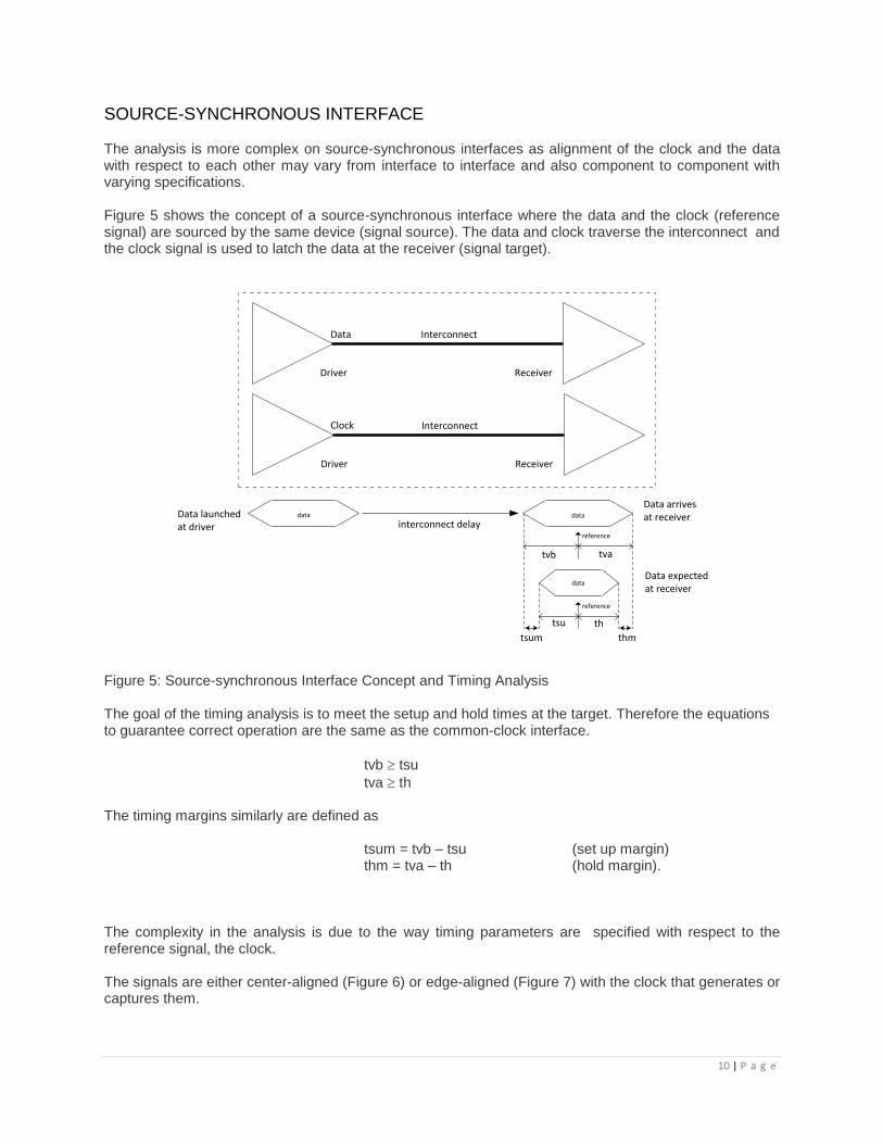
SOURCE-SYNCHRONOUS INTERFACE The analysis is more complex on source-synchronous interfaces as alignment of the clock and the data with respect to each other may vary from interface to interface and also component to component with varying specifications. Figure 5 shows the concept of a source-synchronous interface where the data and the clock (reference signal) are sourced by the same device (signal source). The data and clock traverse the interconnect and the clock signal is used to latch the data at the receiver (signal target). Figure 5: Source-synchronous Interface Concept and Timing Analysis The goal of the timing analysis is to meet the setup and hold times at the target. Therefore the equations to guarantee correct operation are the same as the common-clock interface.
tvb tsu
tva th The timing margins similarly are defined as tsum = tvb – tsu (set up margin) thm = tva – th (hold margin). The complexity in the analysis is due to the way timing parameters are specified with respect to the reference signal, the clock.
The signals are either center-aligned (Figure 6) or edge-aligned (Figure 7) with the clock that generates or captures them.
Driver Receiver
Interconnect
Driver Receiver
Interconnect
Data
Clock
data
interconnect delay
tvb tva
data
tsu th
data
tsum thm
reference
reference
Data launched at driver
Data arrives at receiver
Data expected at receiver
11 | P a g e
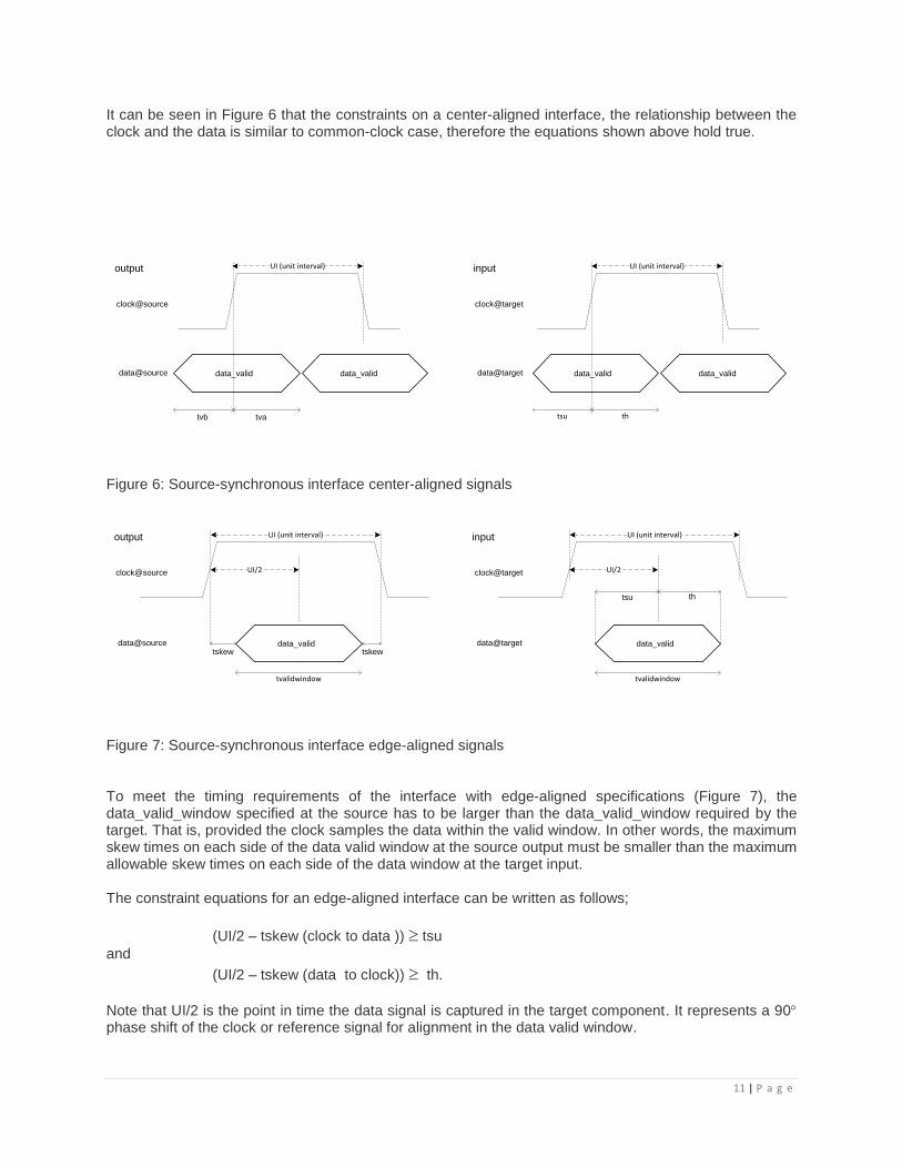
It can be seen in Figure 6 that the constraints on a center-aligned interface, the relationship between the clock and the data is similar to common-clock case, therefore the equations shown above hold true.
Figure 6: Source-synchronous interface center-aligned signals
Figure 7: Source-synchronous interface edge-aligned signals
To meet the timing requirements of the interface with edge-aligned specifications (Figure 7), the data_valid_window specified at the source has to be larger than the data_valid_window required by the target. That is, provided the clock samples the data within the valid window. In other words, the maximum skew times on each side of the data valid window at the source output must be smaller than the maximum allowable skew times on each side of the data window at the target input. The constraint equations for an edge-aligned interface can be written as follows;
(UI/2 – tskew (clock to data )) tsu
and
(UI/2 – tskew (data to clock)) th.
Note that UI/2 is the point in time the data signal is captured in the target component. It represents a 90 phase shift of the clock or reference signal for alignment in the data valid window.
clock@source
data_valid data_valid
data@source
output UI (unit interval)
tvatvb
clock@target
tsu
data_valid data_valid
th
data@target
input UI (unit interval)
clock@source
data@source
output UI (unit interval) input
UI/2 clock@target
tvalidwindow
data@target
UI (unit interval)
data_valid
th
UI/2
tvalidwindow
data_valid
tsu
tskew tskew

12 | P a g e
In the QSI timing files (.tmg files) data-to-clock relationships at the output of the source are described with a DELAY_SKEW statement and at the target with a SETHLD statement, Figure 8.
Figure 8: Timing Relationship between the Data and Clock Signals at the Driver and Receiver in a Source-Synchronous Interface Source (output) “_SKEW_MIN” and “_SKEW_MAX” parameters Target (input) “_SETUP” and “_HOLD” parameters Figure 9: Definition of “_SKEW_MIN”, “_SKEW_MAX”, “_SETUP” and “_HOLD” parameters for center- aligned signal relationship
Data
Clock (reference signal)
DELAY_SKEW SETHLD
data_validdata@source
clock@source
RSKEW_MIN
RSKEW_MAX
FSKEW_MIN
FSKEW_MAX
data_invaliddata_validdata_invalid
UI
data_validdata@target
clock@target
_RSETUP
data_invaliddata_validdata_invalid
_RHOLD _FSETUP
_FHOLD

13 | P a g e
The timing parameters are entered with the delay-skew and sethld statements in the QSI .tmg files with values (depending on whether the signals are center-aligned on edge-aligned) as described in general form below: DELAY_SKEW R CLOCK *TO DATA DATA_RSKEW_MIN DATA_RSKEW_MAX DELAY_SKEW F CLOCK *TO DATA DATA_FSKEW_MIN DATA_FSKEW_MAX SETHLD DATA *TO R CLOCK DATA_RSETUP DATA_RHOLD SETHLD DATA *TO F CLOCK DATA_FSETUP DATA_FHOLD DELAY_SKEW statement defines data-invalid window with respect to the clock at the driver with respect to standard load. SETHLD statement defines data-to-clock setup and hold requirement at the receiver. The parameters “_SKEW”, “_SETUP” and “_HOLD” are defined, for center-aligned and edge-aligned signals as shown in Figures 9 and 10 respectively. In most cases the datasheet does not provide timing parameters in the form that QSI requires. Hence these datasheet parameters need to be expressed in a format QSI can use. Data sheet timing parameters have to be translated into “_SKEW” , “_SETUP” and “_HOLD” values such that QSI can calculate the margins correctly. Source (output) _SKEW_MIN and _SKEW_MAX parameters Target (input) “_SETUP” and “_HOLD” parameters Figure 10: Definition of “_SKEW_MIN”, “_SKEW_MAX”, “_SETUP” and “_HOLD” parameters for edge- aligned signal relationship
data@source
clock@source
data_valid data_invaliddata_invalid
RSKEW_MINRSKEW_MAX
FSKEW_MIN FSKEW_MAX
data@target
clock@target
data_invalid
_RSETUP
UI/2
data_valid data_invalid
_RHOLD
Rising edge clock shifted 900
UI
UI/2
14 | P a g e
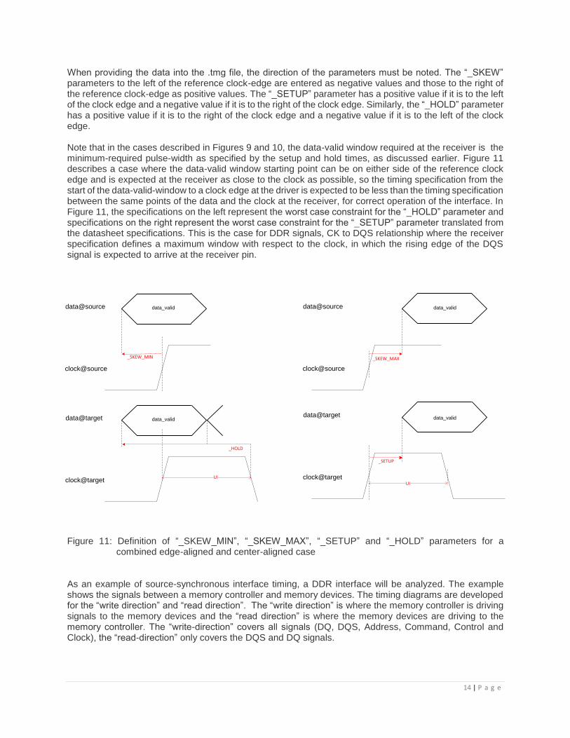
When providing the data into the .tmg file, the direction of the parameters must be noted. The “_SKEW” parameters to the left of the reference clock-edge are entered as negative values and those to the right of the reference clock-edge as positive values. The “_SETUP” parameter has a positive value if it is to the left of the clock edge and a negative value if it is to the right of the clock edge. Similarly, the “_HOLD” parameter has a positive value if it is to the right of the clock edge and a negative value if it is to the left of the clock edge. Note that in the cases described in Figures 9 and 10, the data-valid window required at the receiver is the minimum-required pulse-width as specified by the setup and hold times, as discussed earlier. Figure 11 describes a case where the data-valid window starting point can be on either side of the reference clock edge and is expected at the receiver as close to the clock as possible, so the timing specification from the start of the data-valid-window to a clock edge at the driver is expected to be less than the timing specification between the same points of the data and the clock at the receiver, for correct operation of the interface. In Figure 11, the specifications on the left represent the worst case constraint for the “_HOLD” parameter and specifications on the right represent the worst case constraint for the “_SETUP” parameter translated from the datasheet specifications. This is the case for DDR signals, CK to DQS relationship where the receiver specification defines a maximum window with respect to the clock, in which the rising edge of the DQS signal is expected to arrive at the receiver pin.
Figure 11: Definition of “_SKEW_MIN”, “_SKEW_MAX”, “_SETUP” and “_HOLD” parameters for a combined edge-aligned and center-aligned case As an example of source-synchronous interface timing, a DDR interface will be analyzed. The example shows the signals between a memory controller and memory devices. The timing diagrams are developed for the “write direction” and “read direction”. The “write direction” is where the memory controller is driving signals to the memory devices and the “read direction” is where the memory devices are driving to the memory controller. The “write-direction” covers all signals (DQ, DQS, Address, Command, Control and Clock), the “read-direction” only covers the DQS and DQ signals.
data@target
clock@target
_SETUP
data@source
clock@source
_SKEW_MAX
UI
data_validdata@target
clock@target
_HOLD
data_valid
data@source
clock@source
_SKEW_MIN
data_valid
UI
data_valid

15 | P a g e
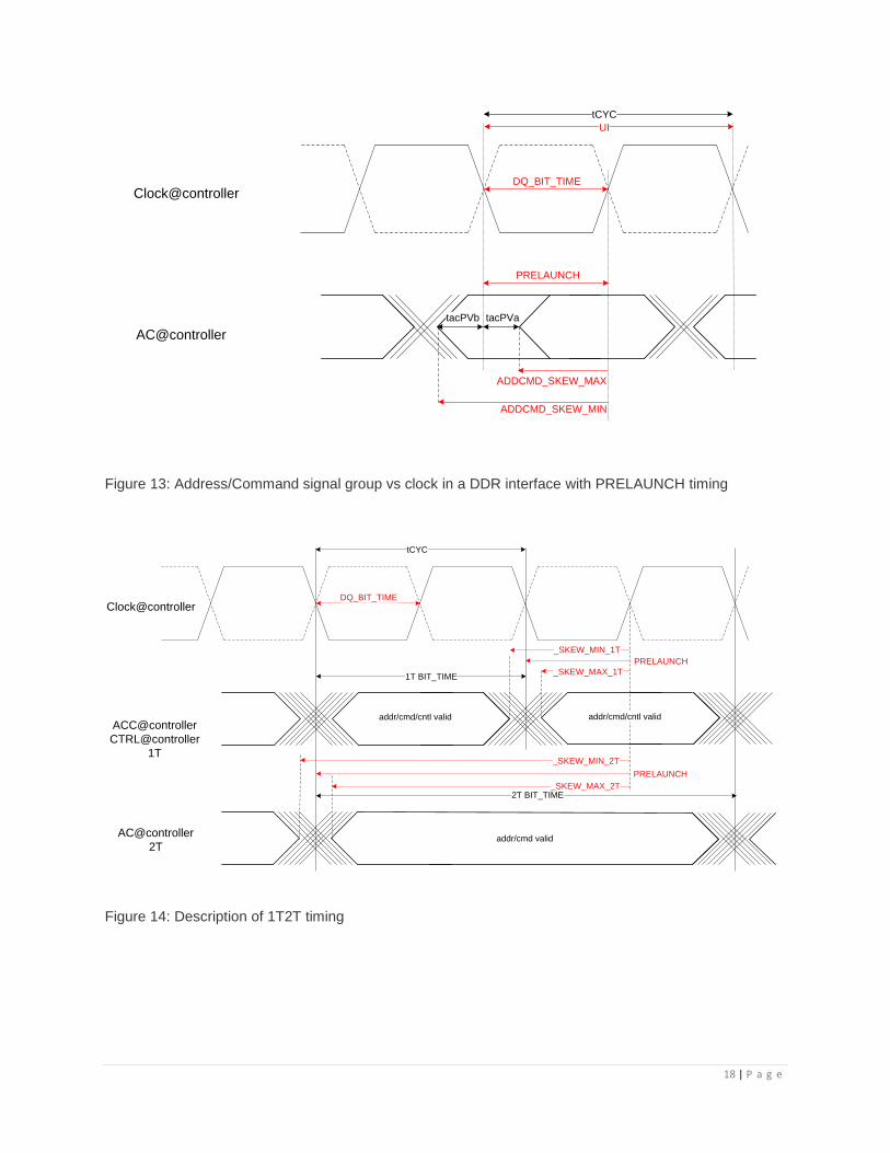
A SOURCE SYNCHRONOUS INTERFACE EXAMPLE: Given below are timing diagrams for a DDR interface, involving address, command, control and data bus signals. A differential clock is used to control the timing of all the signals in the interface. Additionally, a bidirectional strobe signal is used to time the data bus signals in both the “write” and “read” directions. Address/Command/Control (ACC) signals) are captured by the rising edge of the positive component of the differential clock at the memory devices. ACC signals are center-aligned with the clock. The values of the tVB and tVA parameters are specified in the memory controller datasheets and are in general the same for the address and command signals; however, they may be different for the control signals, specifically when the address and command signals are produced by the earlier clock edge for heavily loaded configurations (1T, 2T timing). In heavily-loaded interfaces the address and command signals are connected to all memory components as opposed to control signals connected to a smaller number of components being selected for data transmission depending on the data bus width. With “1T” clocking, a new address and command can be issued on every clock cycle. “2T” timing holds the address and command bus valid for two clock cycles. Figure 12 below shows the ACC signal with respect to the interface clock at the driver and also the receiver end with the datasheet parameters normally specified. Additionally, the parameters entered into the QSI timing files (.tmg files) are marked on the diagrams as they are calculated from the datasheet parameters. QSI calculates the delays from the driver to the receiver. Based on the interconnect delay values that QSI determines through simulations and the parameters entered into the timing file, setup margin and hold margin calculations are done using the equations derived from the parameters as shown on the diagram. Only the rising edge of the clock is used to generate and capture the signal. However timing is analyzed on both the rising and falling transitions of the ACC signals with reference to the rising edge of the clock. QSI uses the following final equations to determine the margins:
Data R/F
Clock R/F
Margin QSI Equation
R R setup RminC – RmaxD – RmaxDS – Rsetup
R R hold UI + RminD + RminDS – RmaxC – Rhold - Jitter
F R setup RminC – FmaxD – RmaxDS – Rsetup
F R hold UI + FminD + RminDS – RmaxC – Rhold - Jitter where UI corresponds to the clock period RminC corresponds to “Min Clock Etch Delay” RmaxC corresponds to “Max Clock Etch Delay” RmaxD corresponds to “Max ACC Etch Delay – rising edge” FmaxD corresponds to “Max ACC Etch Delay – falling edge” RminD corresponds to “Min ACC Etch delay – rising edge” FminD corresponds to “Min ACC Etch delay – falling edge” RmaxDS corresponds to “ _Skew_Max with respect to clock rising edge” RminDS corresponds to “ _Skew_Min with respect to clock rising edge” Rsetup corresponds to “ _Setup to clock rising edge” Rhold corresponds to “_Hold from clock rising edge” Jitter corresponds to “Jitter” (cycle-to-cycle jitter)
16 | P a g e
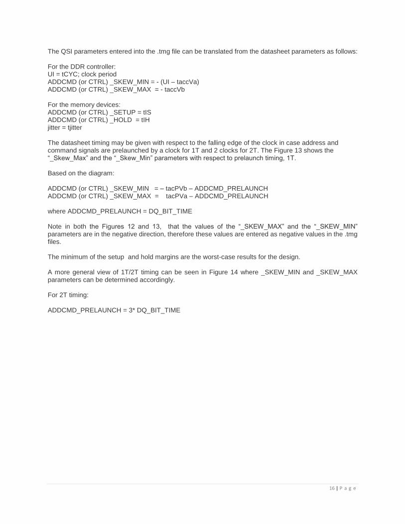
The QSI parameters entered into the .tmg file can be translated from the datasheet parameters as follows: For the DDR controller: UI = tCYC; clock period ADDCMD (or CTRL) _SKEW_MIN = - (UI – taccVa) ADDCMD (or CTRL) _SKEW_MAX = - taccVb For the memory devices: ADDCMD (or CTRL) _SETUP = tIS ADDCMD (or CTRL) _HOLD = tIH jitter = tjitter The datasheet timing may be given with respect to the falling edge of the clock in case address and command signals are prelaunched by a clock for 1T and 2 clocks for 2T. The Figure 13 shows the “_Skew_Max” and the “_Skew_Min” parameters with respect to prelaunch timing, 1T. Based on the diagram: ADDCMD (or CTRL) _SKEW_MIN = – tacPVb – ADDCMD_PRELAUNCH ADDCMD (or CTRL) _SKEW_MAX = tacPVa – ADDCMD_PRELAUNCH where ADDCMD_PRELAUNCH = DQ_BIT_TIME Note in both the Figures 12 and 13, that the values of the “_SKEW_MAX” and the “_SKEW_MIN” parameters are in the negative direction, therefore these values are entered as negative values in the .tmg files. The minimum of the setup and hold margins are the worst-case results for the design. A more general view of 1T/2T timing can be seen in Figure 14 where _SKEW_MIN and _SKEW_MAX parameters can be determined accordingly. For 2T timing: ADDCMD_PRELAUNCH = 3* DQ_BIT_TIME

17 | P a g e
Figure 12: Address/Command/Control signal group vs clock in a DDR interface
taccVb taccVa
tIS tIH
tfltACCmax
(Max ACC
Etch Delay )ADDCMD_SKEW_MIN
ADDCMD_SKEW_MAX
tfltACCmin
(Min ACC
Etch Delay )
Hmargin
CTRL_SKEW_MAX
CTRL_SKEW_MIN
ADDCMD_SETUP
CTRL_SETUP
ADDCMD_HOLD
CTRL_HOLD
Clock@controller
ACC@controller
CTRL@controller
ACC@memory
CTRL@memory
Clock@memory
tclk interconnect delay min
(Min Clock Etch Delay)
tclk interconnect delay max
(Max Clock Etch Delay)
tjitter
tsum = taccVb – tfltACCmax + tclk interconnect delay min – tIS
thm = taccVa + tfltACCmin – tclk interconnect delay max – tIH – tjitter
tCYC
UI jitter
SUmargin
BLACK line arrows and labels: Data sheet parameters or calculated or simulated parameters
RED line arrows and labels: QSI parameters – used in .tmg files – translated from data-sheet parameters
BLUE line arrows and labels: Delays determined by QSI simulations
GREEN line arrows and labels: (r) rising edge, (f) falling or () both rising and falling edge setup, hold margin
Dashed lines point to labels
ADDCMD_SKEW_MIN CTRL_SKEW_MIN
18 | P a g e
Figure 13: Address/Command signal group vs clock in a DDR interface with PRELAUNCH timing
DQ_BIT_TIME
Clock@controller
ACC@controller
CTRL@controller
1T
tCYC
AC@controller
2T
1T BIT_TIME
2T BIT_TIME
_SKEW_MIN_1T
_SKEW_MAX_1T
_SKEW_MAX_2T
_SKEW_MIN_2T
addr/cmd valid
addr/cmd/cntl valid addr/cmd/cntl valid
PRELAUNCH
PRELAUNCH
Figure 14: Description of 1T2T timing
DQ_BIT_TIME
ADDCMD_SKEW_MIN
ADDCMD_SKEW_MAX
Clock@controller
AC@controller
tCYC
UI
tacPVb tacPVa
PRELAUNCH
19 | P a g e
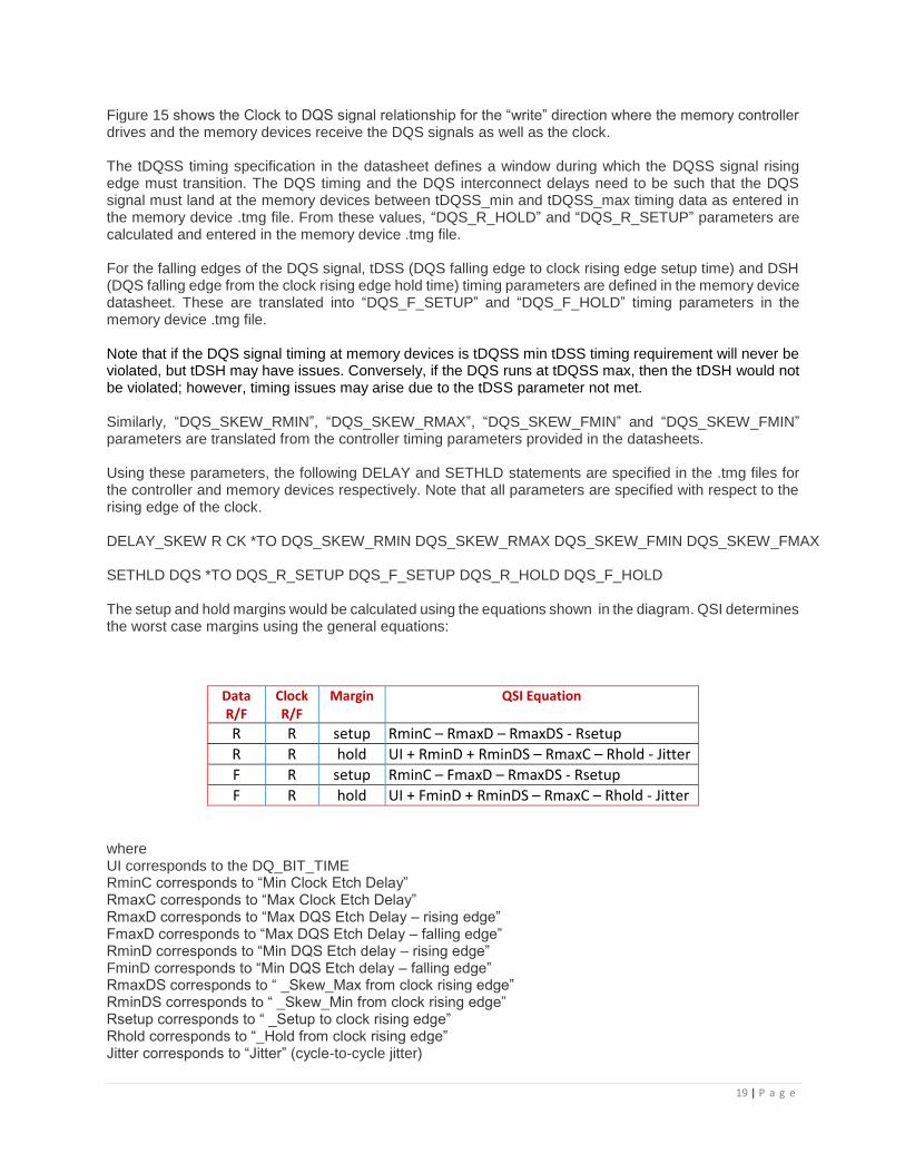
Figure 15 shows the Clock to DQS signal relationship for the “write” direction where the memory controller drives and the memory devices receive the DQS signals as well as the clock. The tDQSS timing specification in the datasheet defines a window during which the DQSS signal rising edge must transition. The DQS timing and the DQS interconnect delays need to be such that the DQS signal must land at the memory devices between tDQSS_min and tDQSS_max timing data as entered in the memory device .tmg file. From these values, “DQS_R_HOLD” and “DQS_R_SETUP” parameters are calculated and entered in the memory device .tmg file. For the falling edges of the DQS signal, tDSS (DQS falling edge to clock rising edge setup time) and DSH (DQS falling edge from the clock rising edge hold time) timing parameters are defined in the memory device datasheet. These are translated into “DQS_F_SETUP” and “DQS_F_HOLD” timing parameters in the memory device .tmg file. Note that if the DQS signal timing at memory devices is tDQSS min tDSS timing requirement will never be violated, but tDSH may have issues. Conversely, if the DQS runs at tDQSS max, then the tDSH would not be violated; however, timing issues may arise due to the tDSS parameter not met. Similarly, “DQS_SKEW_RMIN”, “DQS_SKEW_RMAX”, “DQS_SKEW_FMIN” and “DQS_SKEW_FMIN” parameters are translated from the controller timing parameters provided in the datasheets. Using these parameters, the following DELAY and SETHLD statements are specified in the .tmg files for the controller and memory devices respectively. Note that all parameters are specified with respect to the rising edge of the clock. DELAY_SKEW R CK *TO DQS_SKEW_RMIN DQS_SKEW_RMAX DQS_SKEW_FMIN DQS_SKEW_FMAX SETHLD DQS *TO DQS_R_SETUP DQS_F_SETUP DQS_R_HOLD DQS_F_HOLD The setup and hold margins would be calculated using the equations shown in the diagram. QSI determines the worst case margins using the general equations:
Data R/F
Clock R/F
Margin QSI Equation
R R setup RminC – RmaxD – RmaxDS - Rsetup
R R hold UI + RminD + RminDS – RmaxC – Rhold - Jitter
F R setup RminC – FmaxD – RmaxDS - Rsetup
F R hold UI + FminD + RminDS – RmaxC – Rhold - Jitter where UI corresponds to the DQ_BIT_TIME RminC corresponds to “Min Clock Etch Delay” RmaxC corresponds to “Max Clock Etch Delay” RmaxD corresponds to “Max DQS Etch Delay – rising edge” FmaxD corresponds to “Max DQS Etch Delay – falling edge” RminD corresponds to “Min DQS Etch delay – rising edge” FminD corresponds to “Min DQS Etch delay – falling edge” RmaxDS corresponds to “ _Skew_Max from clock rising edge” RminDS corresponds to “ _Skew_Min from clock rising edge” Rsetup corresponds to “ _Setup to clock rising edge” Rhold corresponds to “_Hold from clock rising edge” Jitter corresponds to “Jitter” (cycle-to-cycle jitter)
20 | P a g e
Figure 15: Clock to DQS Signal Relationship at the Memory Controller and Memory Devices
Jitter Jitter
tjitter tjitter
DQ_BIT_TIME
tclk interconnect delay min
(Min Clock Etch Delay)
tdqsSkewmin
DQS_SKEW_RMAX
tDQSSmin
tDQSSmax
DQS_R_SETUP
tDSS tDSH
DQS_F_SETUP
Clock@controller
DQS@controller
DQS@memory
Clock@memory
tclk interconnect delay max
(Max Clock Etch Delay)
DQS_SKEW_FMIN
DQS_SKEW_FMAX
tdqsSkewmax
tdqsSkewmin
tdqsSkewmax
UI
tdqs interconnect delay min
(Min DQS Etch Delay)
DQS_R_HOLD
tCYC
rtsum (rSUmargin) = – tdqsSkewmax – tdqs interconnect delay max + tclk interconnect delay min + tDQSS_max
rthm (rHmargin) = – tdqsSkewmin + tdqs interconnect delay min – tclk interconnect delay max + tDQSS_max – Jitter
ftsum (fSUmargin) = 1/2tCYC – tdqsSkewmax – tdqs interconnect delay max + tclk interconnect delay min – tDSS
fthm (fHmargin) = 1/2tCYC – tdqsSkewmin + tdqs interconnect delay min – tclk interconnect delay max – tDSH – Jitter
Max Clock Etch Delay – Min
Clock Etch delay + Jitter
tDSH
DQS_F_HOLD
Max Clock Etch Delay – Min
Clock Etch delay + Jitter
fSUmargin
fHmargin
tDQSS_max
rSUmarginrHmargin
BLACK line arrows and labels: Data sheet parameters
RED line arrows and labels: QSI parameters – used in .tmg files – translated from data-sheet parameters
BLUE line arrows and labels: Delays determined by QSI simulations
GREEN line arrows and labels: (r) rising edge, (f) falling or () both rising and falling edge setup, hold margin
Dashed lines point to labels
tDQSS_min
DQS_SKEW_RMIN
tdqs interconnect delay max
(Max DQS Etch Delay)
21 | P a g e
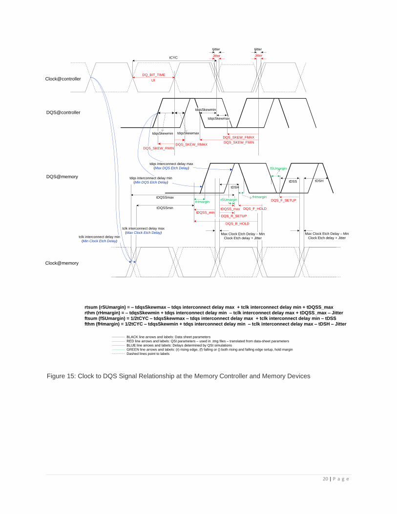
From the diagram, it can be written for the controller that: DQS_SKEW_RMIN = - tdqsSkewmin DQS_SKEW_RMAX = tdqsSkewmax DQS_SKEW_FMIN = - tdqsSkewmin – DQ_BIT_TIME DQS_SKEW_FMAX = tdqsSkewmax – DQ_BIT_TIME and similarly for the memory devices that: DQS_R_SETUP = -tDQSS_max DQS_R_HOLD = tDQSS_min + DQ_BIT_TIME Note the value of tDQSS_min is negative. See below. DQS_F_SETUP = tDSS DQS_F_HOLD = tDSH – DQ_BIT_TIME where, from memory device datasheets: tDQSS_min = tDQSSmin (datasheet) – clock period = – 0.25 * clock_period tDQSS_max = tDQSSmax (datasheet) – clock period = 0.25 * clock_period Note in the diagram that the values of the “DQS_Skew_FMax” and the “DQS_Skew_FMin” and “DQS_Skew_RMIN” parameters and also “_R_SETUP”, “_RHOLD”, “_FHOLD” parameters are in the negative direction, therefore these values are entered as negative values in the .tmg files. Figure 16 describes the timing for the DQS and DQ (and DM) signals for a write operation where the controller drives both the DQS and DQ signals and the memory devices receive them. The timing relationship between DQS and DQ are given in the controller and memory devices datasheets. Note that “DQ_SKEW_MIN” and “DQ_SKEW _MAX” parameters need to have negative values after being translated from datasheet parameters. Also note that data, DQ signal is sampled at both the rising edge and the falling edge of the DQS signal. Therefore, the DELAY_SKEW and SETHLD statements will be provided for the rising and falling edges separately as follows: For the controller: DELAY_SKEW R DQS *TO DQ DQ_SKEW_MIN DQ_SKEW_MAX DELAY_SKEW F DQS *TO DQ DQ_SKEW_MIN DQ_SKEW_MAX And for the memory devices: SETHLD DQ *TO R DQS DQ_SETUP DQ_HOLD SETHLD DQ *TO F DQS DQ_SETUP DQ_HOLD The setup and hold margins would be calculated using the equations shown in the diagram. The QSI determines the worst case margins using the general equations:
22 | P a g e
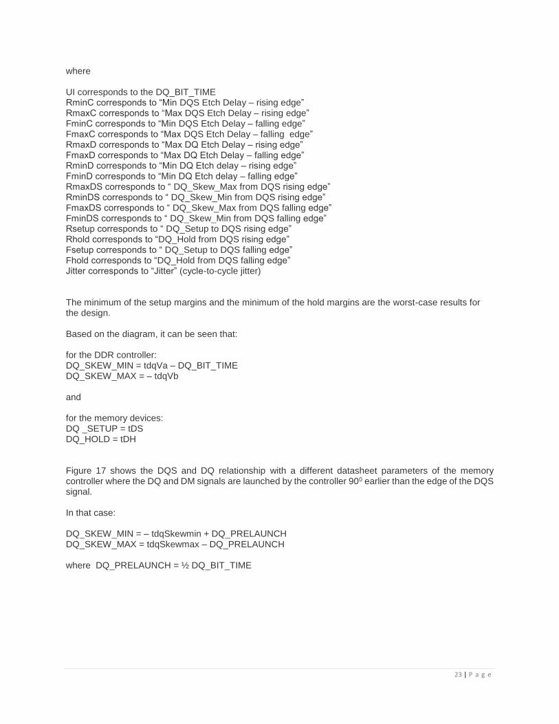
Figure 16: DQS to DQ Signal Relationship at the Memory Controller and Memory Devices for a “Write” Operation
Data R/F
Clock R/F
Margin QSI Equation
R R setup RminC – RmaxD – RmaxDS - Rsetup
R R hold UI + RminD + RminDS – RmaxC – Rhold - Jitter
R F setup FminC – RmaxD – FmaxDS - Rsetup
R F hold UI + RminD + FminDS – FmaxC – Fhold - Jitter
F R setup RminC – FmaxD – RmaxDS - Rsetup
F R hold UI + FminD + RminDS – RmaxC – Rhold - Jitter
F F setup FminC – FmaxD – FmaxDS - Fsetup
F F hold UI + FminD + FminDS – FmaxC – Fhold - Jitter
tdqVb tdqVa
tDS tDH
DQ_BIT_TIME
tfltDQmax
(Max DQ
Etch Delay )DQ_SKEW_MIN
DQ_SKEW_MAX tfltDQmin
(Min DQ
Etch Delay )
DQS interconnect delay max
(Max DQS Etch Delay)
DQS interconnect delay min
(Min DQS Etch Delay)
HmarginSUmargin
DQ_SETUP
DQ_HOLD
DQS@controller
DQ@controller
DQ@memory
DQS@memory
Jitter
DQ_SKEW_MIN
DQ_SKEW_MAX
tsum = tdqVb – tfltDQmax + tDQS interconnect delay min – tDS
thm = tdqVa + tfltDQmin – tDQS interconnect delay max – tDH – Jitter
BLACK line arrows and labels: Data sheet parameters
RED line arrows and labels: QSI parameters – used in .tmg files – translated from data-sheet parameters
BLUE line arrows and labels: Delays determined by QSI simulations
GREEN line arrows and labels: (r) rising edge, (f) falling or () both rising and falling edge setup, hold margin
Dashed lines point to labels
tjitter
tsum thm
23 | P a g e
where UI corresponds to the DQ_BIT_TIME RminC corresponds to “Min DQS Etch Delay – rising edge” RmaxC corresponds to “Max DQS Etch Delay – rising edge” FminC corresponds to “Min DQS Etch Delay – falling edge” FmaxC corresponds to “Max DQS Etch Delay – falling edge” RmaxD corresponds to “Max DQ Etch Delay – rising edge” FmaxD corresponds to “Max DQ Etch Delay – falling edge” RminD corresponds to “Min DQ Etch delay – rising edge” FminD corresponds to “Min DQ Etch delay – falling edge” RmaxDS corresponds to “ DQ_Skew_Max from DQS rising edge” RminDS corresponds to “ DQ_Skew_Min from DQS rising edge” FmaxDS corresponds to “ DQ_Skew_Max from DQS falling edge” FminDS corresponds to “ DQ_Skew_Min from DQS falling edge” Rsetup corresponds to “ DQ_Setup to DQS rising edge” Rhold corresponds to “DQ_Hold from DQS rising edge” Fsetup corresponds to “ DQ_Setup to DQS falling edge” Fhold corresponds to “DQ_Hold from DQS falling edge” Jitter corresponds to “Jitter” (cycle-to-cycle jitter) The minimum of the setup margins and the minimum of the hold margins are the worst-case results for the design. Based on the diagram, it can be seen that: for the DDR controller: DQ_SKEW_MIN = tdqVa – DQ_BIT_TIME DQ_SKEW_MAX = – tdqVb and for the memory devices: DQ _SETUP = tDS DQ_HOLD = tDH Figure 17 shows the DQS and DQ relationship with a different datasheet parameters of the memory controller where the DQ and DM signals are launched by the controller 900 earlier than the edge of the DQS signal. In that case: DQ_SKEW_MIN = – tdqSkewmin + DQ_PRELAUNCH DQ_SKEW_MAX = tdqSkewmax – DQ_PRELAUNCH where DQ_PRELAUNCH = ½ DQ_BIT_TIME
24 | P a g e
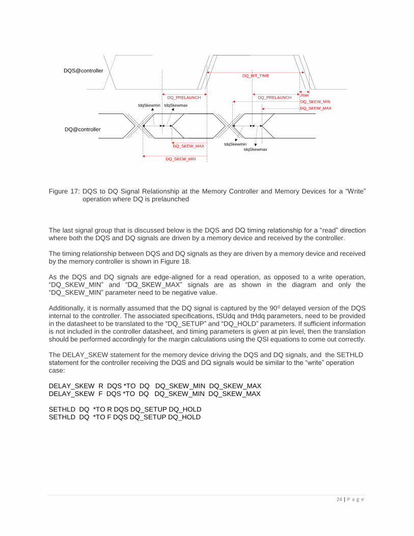
Figure 17: DQS to DQ Signal Relationship at the Memory Controller and Memory Devices for a “Write” operation where DQ is prelaunched The last signal group that is discussed below is the DQS and DQ timing relationship for a “read” direction where both the DQS and DQ signals are driven by a memory device and received by the controller. The timing relationship between DQS and DQ signals as they are driven by a memory device and received by the memory controller is shown in Figure 18. As the DQS and DQ signals are edge-aligned for a read operation, as opposed to a write operation, “DQ_SKEW_MIN” and “DQ_SKEW_MAX” signals are as shown in the diagram and only the “DQ_SKEW_MIN” parameter need to be negative value. Additionally, it is normally assumed that the DQ signal is captured by the 900 delayed version of the DQS internal to the controller. The associated specifications, tSUdq and tHdq parameters, need to be provided in the datasheet to be translated to the “DQ_SETUP” and “DQ_HOLD” parameters. If sufficient information is not included in the controller datasheet, and timing parameters is given at pin level, then the translation should be performed accordingly for the margin calculations using the QSI equations to come out correctly. The DELAY_SKEW statement for the memory device driving the DQS and DQ signals, and the SETHLD statement for the controller receiving the DQS and DQ signals would be similar to the “write” operation case: DELAY_SKEW R DQS *TO DQ DQ_SKEW_MIN DQ_SKEW_MAX DELAY_SKEW F DQS *TO DQ DQ_SKEW_MIN DQ_SKEW_MAX SETHLD DQ *TO R DQS DQ_SETUP DQ_HOLD SETHLD DQ *TO F DQS DQ_SETUP DQ_HOLD
DQ_SKEW_MIN
DQ_SKEW_MAX
DQS@controller
DQ@controller
Jitter
DQ_SKEW_MIN
DQ_SKEW_MAX tdqSkewmin tdqSkewmax
DQ_PRELAUNCH DQ_PRELAUNCH
DQ_BIT_TIME
tdqSkewmin
tdqSkewmax
25 | P a g e
Figure 18: DQS to DQ Signal Relationship at the Memory Controller and Memory Devices for a “Read” Operation The DELAY_SKEW statement for the memory device driving the DQS and DQ signals, and the SETHLD statement for the controller receiving the DQS and DQ signals would be similar to the “write” operation case:
tHdq
DQ_BIT_TIME
DQ_SKEW_MIN
tfltDQmin
(Min DQ
Etch Delay )
DQS interconnect delay max
(Max DQS Etch Delay)
DQS interconnect delay min
(Min DQS Etch Delay)
DQ_SETUP
DQ_HOLD
DQS@memory
DQ@memory
DQ@controller
DQS@controller
tQH
tDQSQ
tCH (min tHP)
DQS@controller
delayed 900
Controller_read
_DQS_Delay
tCYC
DQ_SKEW_MAX DQ_SKEW_MIN
DQ_SKEW_MAX
tfltDQmax
(Max DQ
Etch Delay )
tSUdq
tCL (min tHP)
tsum = – tDQSQ – tfltDQmax + DQS interconnect delay min + 1/2UI – tSUdq
thm = (tCH – tQSH) + tfltDQmin – DQS interconnect delay max – tHdq – 1/2UI – tjitter
Controller_read
_DQS_Delay
Controller_read_DQS_Delay
UI/2
Controller_read
_DQS_Delay
SUmargin Hmargin
DQ_BIT_TIME
UI
Jitter
BLACK line arrows and labels: Data sheet parameters or calculated or simulated parameters
RED line arrows and labels: QSI parameters – used in .tmg files – translated from data-sheet parameters
BLUE line arrows and labels: Delays determined by QSI simulations
GREEN line arrows and labels: (r) rising edge, (f) falling or () both rising and falling edge setup, hold margin
Dashed lines point to labels
tHP
tQHS
Data Valid Window
Clock@memory
tjitter

26 | P a g e
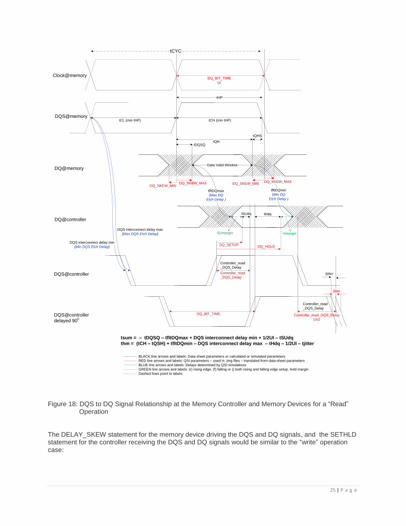
DELAY_SKEW R DQS *TO DQ DQ_SKEW_MIN DQ_SKEW_MAX DELAY_SKEW F DQS *TO DQ DQ_SKEW_MIN DQ_SKEW_MAX SETHLD DQ *TO R DQS DQ_SETUP DQ_HOLD SETHLD DQ *TO F DQS DQ_SETUP DQ_HOLD Given the .tmg file parameters as shown in the diagram, the QSI equations used are:
Data R/F
Clock R/F
Margin QSI Equation
R R setup RminC – RmaxD – RmaxDS - Rsetup
R R hold UI + RminD + RminDS – RmaxC – Rhold - Jitter
R F setup FminC – RmaxD – FmaxDS - Rsetup
R F hold UI + RminD + FminDS – FmaxC – Fhold - Jitter
F R setup RminC – FmaxD – RmaxDS - Rsetup
F R hold UI + FminD + RminDS – RmaxC – Rhold - Jitter
F F setup FminC – FmaxD – FmaxDS - Fsetup
F F hold UI + FminD + FminDS – FmaxC – Fhold - Jitter where UI corresponds to the clock period RminC corresponds to “Min DQS Etch Delay – rising edge” RmaxC corresponds to “Max DQS Etch Delay – rising edge” FminC corresponds to “Min DQS Etch Delay – falling edge” FmaxC corresponds to “Max DQS Etch Delay – falling edge” RmaxD corresponds to “Max DQ Etch Delay – rising edge” FmaxD corresponds to “Max DQ Etch Delay – falling edge” RminD corresponds to “Min DQ Etch delay – rising edge” FminD corresponds to “Min DQ Etch delay – falling edge” RmaxDS corresponds to “ DQ_Skew_Max from DQS rising edge” RminDS corresponds to “ DQ_Skew_Min from DQS rising edge” FmaxDS corresponds to “ DQ_Skew_Max from DQS falling edge” FminDS corresponds to “ DQ_Skew_Min from DQS falling edge” Rsetup corresponds to “ DQ_Setup to delayed-DQS rising edge” Rhold corresponds to “DQ_Hold from delayed-DQS rising edge” Fsetup corresponds to “ DQ_Setup to delayed-DQS falling edge” Fhold corresponds to “DQ_Hold from delayed-DQS falling edge” Jitter corresponds to “Jitter” (cycle-to-cycle jitter) The minimum of the setup margins and the minimum of the hold margins are the worst-case results for the design. Based on the diagram, it can be seen that: for the memory devices: DQ_SKEW_MIN = (tCH – tQHS) – DQ_BIT_TIME DQ_SKEW_MAX = tDQSQ

27 | P a g e
Figure 19: DQS to DQ Signal Relationship at the Memory Controller and Memory Devices for a “Read” Operation – alternative datasheet parameters
DQ_BIT_TIME
DQ_SKEW_MIN
tfltDQmin
(Min DQ
Etch Delay )
DQS interconnect delay max
(Max DQS Etch Delay)
DQS interconnect delay min
(Min DQS Etch Delay)
DQ_SETUP
DQ_HOLD
DQS@memory
DQ@memory
DQ@controller
DQS@controller
tQH
tDQSQ
tCH (min tHP)
Controller_read
_DQS_Delay
tCYC
DQ_SKEW_MAX DQ_SKEW_MIN
DQ_SKEW_MAX
tfltDQmax
(Max DQ
Etch Delay )
tCL (min tHP)
tsum (Sumargin) = – tDQSQ – tfltDQmax + DQS interconnect delay min + tdSkewMax
thm (Hmargin) = (tCH – tQSH) +tfltDQmin – DQS interconnect delay maxy – UI + tdSkewMin – tjitter
Controller_read
_DQS_Delay
UI
BLACK line arrows and labels: Data sheet parameters
RED line arrows and labels: QSI parameters – used in .tmg files – translated from data-sheet parameters
BLUE line arrows and labels: Delays determined by QSI simulations
GREEN line arrows and labels: (r) rising edge, (f) falling or () both rising and falling edge setup, hold margin
Dashed lines point to labels
tHP
tQHS
Data Valid Window
Clock@memory
tdSkewMax
tdSkewMin
SUmargin Hmargin
Jitter
tjitter
28 | P a g e
and for the DDR controller: DQ _SETUP = tSUdq – CONTROLLER_READ_DQS_DELAY DQ_HOLD = tHdq + CONTROLLER_READ_DQS_DELAY Alternatively, the skew requirements of the DQ signals may be given with respect to the DQS signal at the pin of the memory controller in the datasheet. This scenario is described in Figure 19 with the tdSkewMax and tdSKewMin delays. In this case: DQ _SETUP = – tdSkewMax DQ_HOLD = tdSkewMin – DQ_BIT_TIME All other equations would remain the same.
SUMMARY Timing analysis is a critical step in calculating the setup and hold margins for a signal transmission line with a driver and receiver in synchronous systems. The simulation tools offer options to be able to complete the timing analysis; they almost all require some programming and/or correct data entry. Some data translation is definitely required. Considering that timing parameters are described in many different ways in the datasheets, the QSI tool is one of the simulation tools in the market where data translation into the tool is relatively easy.