tiris rf-module ic for automotive ri-rfm-006a - ti.com · tiris rf-moduleic for automotive...
TRANSCRIPT

TIRIS RF-Module IC for AutomotiveRI-RFM-006A
Reference Guide
December 1996
SCBU036

TIRIS RF-Module IC for Automotive
RI-RFM-006A
Reference Guide
Literature Number: SCBU036
December 1996

Contents
1 Overview.................................................................................................................... 42 Features..................................................................................................................... 43 TIRIS™ System Configuration (Schematic Diagram)........................................................ 44 Internal Block Diagram and Pin Assignment .................................................................. 55 Description of Pins...................................................................................................... 66 Function and Operation ............................................................................................... 6
6.1 General ............................................................................................................ 6
6.2 Sending Mode .................................................................................................... 7
6.3 Receiving Mode .................................................................................................. 7
7 Electrical Specifications............................................................................................... 97.1 Absolute Maximum Rating ...................................................................................... 9
7.2 Recommended Operating Conditions........................................................................ 10
8 Input-Output Specifications ........................................................................................ 108.1 Transmitter Signal I/O Timing................................................................................. 10
8.2 Receiver Signal I/O Timing.................................................................................... 11
9 Dimensional Outline Drawing – 16-pin SOP .................................................................. 1210 Applied Circuit Configuration – Example...................................................................... 1211 Typical Transmitter Circuit Configuration..................................................................... 1312 Typical Receiver Circuit Configuration......................................................................... 1413 Typical Antenna Circuit Configuration ......................................................................... 1514 Precautions for Mounting and Actual Use .................................................................... 16
14.1 Power Supply Line ............................................................................................. 16
14.2 Wiring for Antenna Circuit ..................................................................................... 17
15 Package ................................................................................................................... 18
SCBU036–December 1996 Table of Contents 3Submit Documentation Feedback

1 Overview
2 Features
3 TIRIS™ System Configuration (Schematic Diagram)
TIRIS transponder
ControllerSerial
transmission
TIRIS RF-module
RI45538NS
TIRIS Read-Write SystemTransmitter-receiver
Antenna
FSK
ASK
Reference GuideSCBU036–December 1996
TIRIS RF-Module IC for Automotive
RI-RFM-006A is a CMOS-technology based RF-module IC which integrates all transmitter-receiverfunctions required for constructing a TIRIS Read-Write System into one single chip.
RI-RFM-006A consists of a transmitter signal control logic which generates signals for transmission andfor sending the data you wrote to a remote TIRIS transponder, and a receiver amplifies and demodulatesfrequency shift keyed (FSK) signals received from this transponder.
Therefore, RI-RFM-006A is beneficially usable for constructing, in particular, a compact TIRIS Read- WriteSystem at a reduced cost. Furthermore, demodulation of the FSK signals received in its receiver from aremote transponder is entirely digitized; this completely eliminates the need of regulations and lessens thenumber of required external parts, thus enhancing the operational reliability of the system.
The TIRIS RF-Module IC for Automotive Application, RI-RFM-006A, provides the following featuresamongst others:
• It incorporates a transmitter circuit with power selector and an open drain transmission powerpredriver.
• Also incorporated are a receiver signal amplifier and a digitized FSK signal demodulator.• I/O specifications: Conform to TIRIS standard RF-module specifications, with available signals of
TXCT–, RXDT– (1) and RXCK only.• Operating supply voltage: 4.5 V to 5.5 V• Operating temperature range: –40°C to 85°C• Package: 16-pin SO package• Structure: CMOS process
(1) For RXDT– signals, this RF-module has a reverse polarity in relation to TIRIS standard RF-modules. See the section “Description ofPins” for more information.
TIRIS RF-Module IC for Automotive4 SCBU036–December 1996Submit Documentation Feedback

www.ti.com
4 Internal Block Diagram and Pin Assignment
161
2
3
4
5
6
7
8 9
10
11
12
13
14
15DIGITAL
DEMODULATOR
CONTROL
LOGIC
TRANSMITTER
NCH OPEN DRAIN
PCH OPEN DRAIN
MOS INVERTER
MOS INVERTER
MOS INVERTER
A3OP
A3IN
A2OP
A2IN
A1OP
A1IN
TXLO
TXHI OSCI
OSCO
GND
VCC
TPC
TXCT-
RXDT-
RXCK
OSCILLATOR
Internal Block Diagram and Pin Assignment
Name I/O Function Name I/O Function
A3OP CMOS INVERTER-3/FSK SIGNAL OUTPUT OSCI OSCILLATOR INPUT(17.1776MHz typ.)
A3IN CMOS INVERTER-3/FSK SIGNAL INPUT OSCO OSCILLATOR OUTPUT
A2OP CMOS INVERTER-2 OUTPUT GND GND(POWER SUPPLY)
A2IN CMOS INVERTER-2 INPUT VCC VCC(POWER SUPPLY)
A1OP CMOS INVERTER-1 OUTPUT TPC TX-POWER Hi/Lo SELECT SIG. INPUT
A1IN CMOS INVERTER-1 INPUT TXCT– TX-OUTPUT CONTROL SIGNAL INPUT
TXLO TX-OUTPUT(NCH OPEN DRAIN OUTPUT) RXDT– RX-DATA("L"="1","H"="0") OUTPUT
TXHI TX-OUTPUT(PCH OPEN DRAIN OUTPUT) RXCK RX-DATA CLOCK OUTPUT
SCBU036–December 1996 TIRIS RF-Module IC for Automotive 5Submit Documentation Feedback

www.ti.com
5 Description of Pins
6 Function and Operation
6.1 General
Description of Pins
Pin # Signal I/O Description
1 A3OP O Signal output from CMOS inverter-3 amplifier; this pin is connected to the internal FSKsignal digital demodulator.
2 A3IN I Signal input to CMOS inverter-3 amplifier; if an external circuit is used to amplify FSKsignals, the amplified signals are input through this pin.
3 A2OP O Signal output from CMOS inverter-2 amplifier.
4 A2IN I Signal input to CMOS inverter-2 amplifier.
5 A1OP O Signal output from CMOS inverter-1 amplifier.
6 A1IN I I 16. Signal input to CMOS inverter-1 amplifier.
7 TXLO Negative Negative level output of transmission signals; this output drives the n-channel MOSFETopen drain used as antenna driver.
output
8 TXHI Positive open Positive level output of transmission signals; this output drives the p-channel MOSFETdrain output used as antenna driver.
9 OSCI I Signal input to 17.1776 MHz master clock oscillator.
10 OSCO O Signal output from 17.1776 MHz master clock oscillator.
11 GND – Negative power supply.
12 VCC – Positive power supply.
13 TPC I, w/pull-up Input of transmission power selection signals (High-Low). A Low level signal inputresistor through this pin substantially lowers the power during transmission
14 TXCT– I, w/pull-up Input of transmission output control signals (Transmit-Receive Mode Selector). A Lowresistor level signal input through this pin outputs a transmission signal to either “TXLO/TXHI”
pin while a High level signal input turns the mode to Receive and activates the internalFSK signal digital demodulator.
15 RXDT– O Serial output of demodulated FSK signal bit data. Negative level output when the bitdata received from the remote transponder is “1”, and positive level output when it is“0”.Note: The RI-RFM-006A has a reverse polarity in relation to TIRIS standardRF-modules.
16 RXCK O Synchronous clock output of demodulated FSK signal data; a clock signal synchronizedwith the “RXDT-“ signal is output.
This RF-module IC counts on two operating modes:Sending Mode – This mode is active when the “TXCT–“ pin is set to L-level. A remote TIRIStransponder can be charged up and ID code can be sent to that transponder in this mode.Receiving Mode – This mode is active when the “TXCT–“ pin is set to H-level. FSK signals sent from aremote TIRIS transponder are received and demodulated in this mode.
Therefore, by switching over these modes using an external controller, data communications with a TIRIStransponder can be made.
Note that this RF-module IC is exclusively designed to provide the user with a simple signalmodulator-demodulator (modem) function for data communications with a remote TIRIS transponder,based on the appropriate data modulation-demodulation specifications. And therefore, it does notincorporate error detection, data allotment nor other similar data processing functions in terms of protocoland data formats.
6 TIRIS RF-Module IC for Automotive SCBU036–December 1996Submit Documentation Feedback

www.ti.com
6.2 Sending Mode
7 8
RI45538NS
TXLO TXHI
Master clock frequency divided by 128
(Ref. frequency, resulting: 134.2 kHz)
"A"
MOSFET(PCH)
MOSFET(NCH)
6.3 Receiving Mode
Internal master clock
Signals discriminated
at A3OP terminal
Clock counts 11 2 3 4 5 6 XX-1 2 3 4 5 6 7
Function and Operation
(*) In both transmit and receive modes, this RF-module IC modulates and demodulates signals by logicaloperation based on the incorporated master clock. This means that the modulating-demodulatingperformance characteristics of this IC are directly affected by the frequency accuracy and variation of itsmaster clock (normal frequency is 17.1776 MHz). Therefore, the user is requested to select an oscillatingelement or an external clock which is compatible with the remote TIRIS transponder to be used (see thesection describing the specifications “fexc”, “fL” and “fH”).
In the Sending Mode, the frequency of the IC master clock (normal value: 17.1776 MHz) is divided by 128.The resulting clock signal then has a frequency of 134.2 kHz (normal value). This resulting signal is outputas a composite signal for “TXHI” and “TXLO” terminals (pins) to drive the MOSFET which is incorporatedas an antenna resonance circuit driver, as illustrated below.
When the IC is in the Receiving Mode, its “TXHI” terminal is fixed at positive level and the “TXLO” at highimpedance. As a result, the output terminal “A” of the MOSFET used as an antenna resonance circuitdriver is fixed at negative level.
Note that when the IC is in the Sending Mode, its “RXDT–“ terminal is always fixed at positive level and asa consequence, the IC’s FSK signal demodulator remains deactivated although data clock signals, whichare transmitted at a frequency resulting from division of the “A3IN” terminal signal frequency by 16, areoutput to the “RXCK”.
In the Receiving Mode, the frequency-shift-keyed data signals are sequentially digitized to discriminatetheir frequencies by binary notation (high-low) and demodulate them into bit strings consisting of bit data“1” and “0”.
For binary discrimination of signal frequencies between high and low, the frequency level of eachFS-keyed signal is measured from its leading edge at the “A3OP” terminal through to the next leadingedge by count of the internal master clock, as shown below. The threshold for this counted value (x in thediagram below) is fixed at 132; when the clock count is over 132, it results in a negative level output at the“RXDT–“ terminal (bit data ”1”), and when the clock count does not reach 132, a positive level output atthe same terminal (bit data “0”), respectively.
SCBU036–December 1996 TIRIS RF-Module IC for Automotive 7Submit Documentation Feedback

www.ti.com
Internal frequency
discriminating signals
Signal discriminated
at A3OP terminal
RXDT- terminal
output signals
DATA VALID DATA VALID
A3OP terminal signal
RXCK terminal output
DATA VALIDRXDT- terminal output
15 16 1 2 3 4 5 6 7 8 9 10 11 12 13 14 15 16 1 2 3
One bit data group (16 waves)
4 waves 4 waves8 waves
Function and Operation
As the normal frequency of the internal master clock is 17.1776 MHz, one clock count is equivalent to130.133... kHz (17.1776 MHz divided by 132 = 130.133... kHz). Accordingly, a signal is identified as bitdata “1” with the resulting negative level output at the “RXDT–“ terminal when the signal frequency at the“A3OP” terminal is 130.133... kHz or less, and it is identified as bit data “0” with the resulting positive leveloutput at the “RXDT–“ terminal when the signal frequency at the “A3OP” terminal is over 130.133... kHz.
An additional feature is included to maximize the stability of the above-mentioned FSK signaldemodulating system based on binary notation: the system incorporates a circuit which disables definitionof an “RXDT–“ signal unless more than four consecutive FS-keyed signal waves are identified within thesame frequency band during binary discrimination. This protects the once defined “RXDT–“ signal in thebit data form from being affected by sporadic events. For instance, even when its discrimination result issporadically inverted due to some noise effects, it is not affected if only three or less consecutive FSkeyedsignal waves are identified at the “A3OP” terminal. (See the diagram below.)
Note: For the timing between “A3OP” and “RXDT–“ signals, refer to the section describing “Input-OutputSpecifications”.
The signals demodulated through the above-mentioned process are sequentially output from the “RXDT–“terminal in bit strings (“1” or “0”). To delimit these continuous bit strings, clock signals are output from the“RXCK” terminal in synchronization with each bit data.
In normal operating conditions (when data communication can be properly performed between theRI-RFM-006A and a TIRIS transponder), each bit data group sent from the remote transponder iscomposed of sixteen consecutive signal waves belonging to the same frequency band (consisting of twowave groups, 134.2-kHz high and 123.2-kHz low in terms of normal values). Therefore, clock signals at afrequency resulting from a simple division of the “A3OP” terminal signal frequency by 16, are output fromthe “RXCK” terminal. Then, each “RXCK” clock signal is controlled for output so that its first transition fallsafter four consecutive “A3OP” signal waves from the “RXDT–“ signal change point. This enables anexternal controller to obtain the relevant bit data without fail provided that each “RXDT–“ signal is fetchedwell timed with the first transition of each “RXCK” signal. (See the diagram below.)
8 TIRIS RF-Module IC for Automotive SCBU036–December 1996Submit Documentation Feedback
www.ti.com
A3OP terminal signal
RXCK terminal output
RXDT- terminal output
14 1 2 3 4 5 6 7 8 9 10 11 12 13 14 15 16 1
DATA="0"
16
DATA="1"
1513
(each duration is equivalent to four A3OP terminal
Timing is controlled so that these durations are uniform
7 Electrical Specifications
7.1 Absolute Maximum Rating
Electrical Specifications
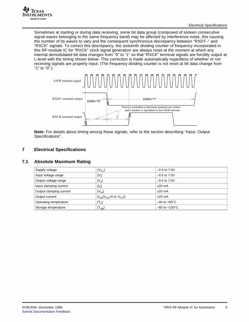
Sometimes at starting or during data receiving, some bit data group (composed of sixteen consecutivesignal waves belonging to the same frequency band) may be affected by interference noise, this causingthe number of its waves to vary and the consequent synchronous discrepancy between “RXDT–“ and“RXCK” signals. To correct this discrepancy, the sixteenth dividing counter of frequency incorporated inthis RF-module IC for “RXCK” clock signal generation are always reset at the moment at which anyinternal demodulated bit data changes from “0” to “1” so that “RXCK” terminal signals are forcibly output atL-level with the timing shown below. This correction is made automatically regardless of whether or notreceiving signals are properly input. (The frequency dividing counter is not reset at bit data change from“1” to “0”.)
Note: For details about timing among these signals, refer to the section describing “Input- OutputSpecifications”.
Supply voltage (VCC) –0.5 to 7.0V
Input voltage range (VI) –0.5 to 7.0V
Output voltage range (Vo) –0.5 to 7.0V
Input clamping current (Iik) ±20 mA
Output clamping current (Vok) ±20 mA
Output current (Iout(Vout=0 to VCC)) ±25 mA
Operating temperature (TA) –40 to +85°C
Storage temperature (Tstg) –65 to +150°C
SCBU036–December 1996 TIRIS RF-Module IC for Automotive 9Submit Documentation Feedback

www.ti.com
7.2 Recommended Operating Conditions
7.2.1 Recommended Operating Conditions
7.2.2 Electrical Characteristics (VCC=5.0V, TA=25°C)
8 Input-Output Specifications
8.1 Transmitter Signal I/O Timing
TXCT-
TXHI+TXLO
tdl(TX)
tc(TX)
twh(TX)
twl(TX) tdh(TX)
TX=
Input-Output Specifications
MIN MAX UNIT
Supply voltage, VCC 3.5 5.5 V
High-level input voltage, VIH 0.7 VCC V
Low-level input voltage, VIL 0.2 VCC V
Operating free-air temperature, TA –40 85 °C
PARAMETER CONDITIONS MIN TYP MAX UNIT
Vth Hysteresis voltage 1.7 V
IOH High-level output current VOH=3.7V 6.8 mA
(TXHI) 20 mA
(A2OP,A3OP) 73 µA
(A1OP) 144 µA
IOL Low-level output current VOH=0.5V –6.8 mA
(TXLO) –20 mA
(A2OP,A3OP) –72 µA
(A1OP) –144 µA
Ci Input capacitance 7.4 pF
ICC Supply current 35 mA
Note: Unless otherwise specified, all the voltage values indicated above are those measured versus the“GND” pin of this RF-module IC.
TIRIS RF-Module IC for Automotive10 SCBU036–December 1996Submit Documentation Feedback

www.ti.com
8.2 Receiver Signal I/O Timing
A3OP
RXCK
RXDT-
tdh(RXCK) tdl(RXCK)
twh(RXCK)
tc(RXCK)
ts(RXDT)
tw(RXDT)
th(RXDT)
twh(A3OP) tc(A3OP)
DATA VALID
td(RXDT)
Input-Output Specifications
ITEM SIGNAL MIN TYP MAX UNIT
Delay time between TXCT– and TX trailing edges tdl(TX) 64Tc(OSC) nS
Delay time between TXCT– and TX leading edges tdh(TX) 1Tc(OSC) nS
TX cycle time tc(TX) 128Tc(OSC) nS
TX low level pulse duration twl(TX) 64Tc(OSC) nS
TX high level pulse duration twh(TX) 64Tc(OSC) nS
Note: “Tc(osc)" denotes the master clock cycle of this RF-module IC and its normal value is specified at56.3 ns (1/0.0171776). The same applies hereinafter. “TX” is defined as a composite signal of “TXLO” and“TXHI” signals.
ITEM SIGNAL MIN TYP MAX UNIT
A3OP cycle time for normal FSK signal demodulation tc(A3OP) 2Tc(OSC) nS
A3OP positive level pulse duration for normal FSK signal twh(A3OP) 1Tc(OSC) nSdemodulation
A3OP cycle time for negative level output of RXDT– tc(A3OP) 132Tc(OSC) nSsignal (bit data “1”)
Delay time between A3OP and RXCK leading edges tdh(RXCK) 1Tc(OSC) nS
Delay time between A3OP leading edge and RXCK tdl(RXCK) 1Tc(OSC) nStrailing edge
RXCK cycle time tc(RXCK) 16Tc(A3) nS
RXCK positive level pulse duration twh(RXCK) 8Tc(A3) nS
Delay time from consecutive A3OP identical signal td(RXDT) 16Tc(A3)+1Tc(OSC) nSwaves to definition of an RXDT– signal
RXDT– positive/negative level duration, definite tw(RXDT) 16Tc(A3) nS
RXDT– signal setup time in relation to RXCK signal ts(RXDT) 4Tc(A3)—1Tc(OSC nS)
RXDT– signal hold time in relation to RXCK signal th(RXDT) 4Tc(A3)–1Tc(OSC) nS
SCBU036–December 1996 TIRIS RF-Module IC for Automotive 11Submit Documentation Feedback

www.ti.com
9 Dimensional Outline Drawing – 16-pin SOP
(Dimensions in mm)
9.90~10.50
0.81(MAX) 0.35~0.510.25
1.27(TYP)
5.00~5.60 7.40~8.20
0 - 10 0.55~1.05
2.00(MAX)
0.05(MIN)0.10
–’PˆÊ‚Í‚ ‚
1 8
916
S57780 MAYMLLLLJ
0.15(TYP)
RI45538NS
10 Applied Circuit Configuration – Example
Dimensional Outline Drawing – 16-pin SOP
Note: “Tc(A3)” denotes the signal cycle at the “A3OP” terminal and the above values are based on thecondition that a bit data group composed of sixteen consecutive signal waves belonging to the samefrequency band (sent from a remote TIRIS transponder in normal operating conditions) has beenpreviously input; otherwise, the values shown in the table below shall apply.
ITEM SIGNAL MIN TYP MAX UNIT
RXCK cycle time (except for normal signal receiving) tc(RXCK) 9Tc(A3) nS
RXCK positive level pulse duration (except for normal signal receiving) twh(RXCK) 1Tc(A3) nS
RXDT– positive/negative level duration, definite (except for normal tw(RXDT) 9Tc(A3) nSsignal receiving)
Shown below is an example of applied circuit configuration for constructing a TIRIS Transmit-ReceiveRF-module using the RI-RFM-006A. This example illustrates a simplified amplifier circuit for receivedsignals by eliminating a frequency band rejection filter which effectively eliminates external noises andsignals out of the frequency band of the response signals from the remote TIRIS transponder. In thisconfiguration, therefore, it is assumed that the available data communication distance of the system couldbe easily affected by environmental conditions.
Note that this is only one of various possible applications. For more information of applied circuitconfigurations, refer to the Application Handbook issued by our TIRIS Operation Dept.
12 TIRIS RF-Module IC for Automotive SCBU036–December 1996Submit Documentation Feedback

www.ti.com
TMS57780NS
910111213141516
51 2 3 4 6 7 8
ANTENNA
VCC
GND
TXCT
RXDT
RXCKNC
1M1200pF
68pF 68pF 68pF 0.01uF 0.01uF 0.01uF
120pF120pF1M 10K 100
1S1588
1S1588
120
100uF0.1uF
17.1776MHz
(*) (*)
2SJ182
2SK974
(L=48uH)
RI45538NS
11 Typical Transmitter Circuit Configuration
Typical Transmitter Circuit Configuration
* When configuring an applied circuit, take the following into account:
• Choose the capacity of a resonance capacitor for clock generator oscillator in accordance with theoscillator characteristics.
• Define the frequency accuracy and variation of the clock generator oscillator by conversion based onthe specifications for the TIRIS transponder to be used together so that it can be within the range of17.17248 MHz to 17.18272 MHz (standard frequency: 17.1776 MHz).
• Select the values at resonance points around 134.2 kHz for L and C of the antenna circuit,respectively. (In the example illustrated above, the following combination is used: antenna: 48 µH;capacitor: 0.03 µF = 0.01 µF × 3 units)
• It is desirable to use a MOSFET having a low on-state resistance for antenna driver
This RF-module IC is provided with “TXHI” and “TXLO” terminals which can drive external MOSFETs fordriving the LC serial resonance antenna circuit. This resonance antenna circuit is to send 134.2-kHzsignals to the remote TIRIS transponder. Use these terminals as illustrated below.
SCBU036–December 1996 TIRIS RF-Module IC for Automotive 13Submit Documentation Feedback

www.ti.com
RI45538NS
To receiving circuit
R17
TXLO
8TXHI
LC resonance circuitGND VCC
134.2KHz
C1
L1
T1
T2Antenna
12 Typical Receiver Circuit Configuration
Typical Receiver Circuit Configuration
In this circuit configuration, by selecting a value for R1 within a range of several hundred ohms and inaccordance with the characteristics of MOSFETs (T1 and T2) and introducing the selected value, thethrough current which is consumed by the MOSFETs themselves during transmission can be reduced. Ifthe value for R1 is too high, the on-state resistances of T1 and T2 become very high and they will havedifficulty in driving the LC resonance circuit, leading to a possible reduction of available datacommunication distance. Therefore, it is recommended that the value for R1 be defined after carefulevaluation of the characteristics of T1 and T2.
L1 and C1 in the LC resonance circuit may be mutually exchanged in position without giving significantadverse effects to the operating performance of the circuit. However, the connection as is as illustratedabove is most preferable since it reduces potential influence of high-voltage transmission signals producedat C1 on T1 and T2, thus a higher efficiency is gained.
Three simple CMOS inverter type amplifiers are integrated in this RF-module IC in order to amplify theFSK signals received from a remote TIRIS transponder up to a satisfactory logic level. The IC is designedso as to permit their amplification factor and frequency characteristics to be selected within a certain rangeby the use of appropriate external parts and/or circuits. A typical applied receiver circuit is illustratedbelow.
14 TIRIS RF-Module IC for Automotive SCBU036–December 1996Submit Documentation Feedback

www.ti.com
1 2 3 4 5 6
To FSK signal demodulatorRI45538NS
R1 R2 R3 R4
C1
C2 C4
C5
A3OP A3IN A2OP A2IN A1OP A1IN
From Antenna
C3
D2
D1
C6
13 Typical Antenna Circuit Configuration
fLC
( )134.2KHz =
1
2π
Typical Antenna Circuit Configuration
In general, the FSK signals sent from a remote TIRIS transponder are found within a band of 120 kHz to140 kHz, mainly due to dispersion of workmanship during manufacture and ambient temperaturefluctuation during transmitting operation. Therefore, by damping signals that fall out of the above bandrange as much as possible, noise suppression performance can be improved. In the illustrated circuitconfiguration, amplifier input coupling capacitors C2, C4 and C6 are used to reduce extremelylow-frequency noise signals, and amplifier output load capacitors C1, C3 and C5 to reduce high-frequencynoises. If you desire to enhance the noise resistance of the circuit still more, it is necessary to install arequired number of external wide band amplifiers with high amplification factor and add an active bandpass filter, LC resonance circuit, etc.
D1, D2 and R4 for input into the first amplifier (A1) form a circuit to prevent high-voltage signals for powertransmission and similar signals from entering the IC, thereby keeping from occurrence of latch-up orother adverse situations. This circuit or otherwise, an equivalent protector, must be inserted without fail.
The antenna circuit consisting of L and C illustrated earlier in this manual (see the section describing“Applied Circuit Configuration – Example”) is designed to work as an LC serial resonance circuit in whichimpedance drops in the presence of resonance frequencies during sending operation, and as an LCparallel resonance circuit in which impedance increases in the presence of resonance frequencies duringreceiving operation. The relationship between L and C incorporated in the resonance circuit can bedefined according to the following expression. Each value is calculated using this expression:
The higher the Q value (quality factor) is, the higher transmission power the antenna L obtains and alsothe higher the receiving gain becomes, thus allowing the system to have a greater available datacommunication distance. If, however, at switch-over from power transmission mode to the receiving mode,damping of the power transmission signal would not be completed before the remote TIRIS transpondersends its ID code back to the IC, the signals sent from the transponder could not be received properly.And the higher the Q value is, the longer the decay time of this power transmission signal will be. It hasbeen revealed by experimental testing that an antenna with its maximum Q value of around 30 is usable inthe circuit as is as illustrated in the “Applied Circuit Configuration – Example” section. If it is desired to usean antenna having a higher Q value, some measures must be devised and added to this circuit.
SCBU036–December 1996 TIRIS RF-Module IC for Automotive 15Submit Documentation Feedback

www.ti.com
14 Precautions for Mounting and Actual Use
14.1 Power Supply Line
Equivalent circuit for internal power supply line feedback loop
Positive power supply (Vcc) line
Feedback loop
Bypass capacitor
From Antenna
1 2 3 4 5 6
16 15 14 13 12 11
Amplifier 1Amplifier 2Amplifier 3
Internal power supply line
Precautions for Mounting and Actual Use
Additionally, the characteristics and efficiency of the resonance circuit used here greatly depend not onlyon the antenna L but also on the capacitor C and the MOSFETs which drive them. Therefore, theapplication of the lowest possible impedance at the frequency f(134.2 kHz) to them will permit a highertransmission power, and as a result, it will allow the system to have a greater available datacommunication distance with the remote transponder.
Described in this section are the precautions to be taken at mounting and actual use of the RI-RFM-006Awhile designing and manufacturing a TIRIS Read-Write System using this IC, especially, critical issues asmay affect the operating performance of the IC and, in particular, the system communication performancewith a remote TIRIS transponder.
When the signals returned from a remote TIRIS transponder are amplified by sequentially using the threeCMOS inverter type amplifiers incorporated in this RF-module IC, an undesirable feedback loop is formedfrom the third amplifier toward the first one through parasitic L, R and C whose formation is not avoidablebecause of the structure of this IC and its internal power supply line (see the diagram below) as CMOSdevices are inevitably bi-directional. If this feedback loop is left as is, it normally leads to an oscillation;particularly, when the frequency band of each amplifier is limited so that it matches that of the transponderreturn signals, oscillation occurs at a frequency within this band which counts on high gains from the verynature of things, in consequence, adversely affecting the demodulating performance of the received FSKsignals.
This situation does not a little occur when a multiple number of high-gain amplifiers are integrated in aCMOS device. Formation of this undesirable feedback loop in the amplifier band can be avoided byminimizing the impedance of the power supply line through optimization of the printed circuit boards andusing a suitable bypass capacitor. It is extremely difficult to obtain true values for these parasitic L, R andC forming the internal power supply line feedback loop, but it can be said from the empirical viewpoint thatit is possible to inhibit the said oscillation using a bypass capacitor with a capacity of 1 µF and having asufficiently low impedance within the said amplifier frequency band provided that appropriate wiringpatterns are defined for the power supply line on the printed circuit boards and in the peripheries ofexternal parts for the amplifiers.
TIRIS RF-Module IC for Automotive16 SCBU036–December 1996Submit Documentation Feedback

www.ti.com
14.2 Wiring for Antenna Circuit
a. When the antenna is driven first.
RI45538NS
7 8
TXLO TXHI
To receiver amplifier
Shielded wire
Antenna
Antenna resonance capacitor
b. When the capacitor is driven first.
RI45538NS
7 8
TXLO TXHI
To receiver amplifier
Shielded wire
Antenna
Antenna resonance capacitor
Precautions for Mounting and Actual Use
As previously described, the FSK signals sent from a remote TIRIS transponder are normally found withina band of 120 kHz to 140 kHz. Therefore, the signal receiving circuit of this TIRIS Transmitter- ReceiverSystem is designed so that the signal amplification factor is necessarily highest within this band. Becauseof this, all signals and noises which are produced by other devices and whose frequencies fall within thisband greatly affect the system performance, especially, its available data communication distance with theremote TIRIS transponder among others.
In the same way, they have quite the undesirable effect not only upon the environment in which the properantenna for the system is found, but also upon the wire used to connect it with the IC’s “A1IN” pin whichworks as the first-phase amplifier for received signals. Furthermore, if there are wires for square or pulsewave logic signals containing high-frequency components (even though their fundamental frequencies arelow) very close to this antenna connection wire, the system’s available data communication distance withthe remote TIRIS transponder is further shortened due to the adverse effects of such wires. For all that, ifthere is no other alternative than to use a long wiring between the IC and its external antenna, it issuggested that a shielded wire be used for antenna wiring in either way as illustrated below. With this, theantenna wiring will be less susceptible to the aforementioned adverse effects.
SCBU036–December 1996 TIRIS RF-Module IC for Automotive 17Submit Documentation Feedback

www.ti.com
15 Package
Texas Instruments
50 pcs./tube
1,000 pcs. (20 tubes/bag)
Silica gel
Antistatic finish poly bag
Aluminum laminated case
Heat-sealed
Bar code label
Corrugated fiberboard case
Destination label
Package
18 TIRIS RF-Module IC for Automotive SCBU036–December 1996Submit Documentation Feedback

IMPORTANT NOTICE
Texas Instruments Incorporated and its subsidiaries (TI) reserve the right to make corrections, modifications,enhancements, improvements, and other changes to its products and services at any time and to discontinueany product or service without notice. Customers should obtain the latest relevant information before placingorders and should verify that such information is current and complete. All products are sold subject to TI’s termsand conditions of sale supplied at the time of order acknowledgment.
TI warrants performance of its hardware products to the specifications applicable at the time of sale inaccordance with TI’s standard warranty. Testing and other quality control techniques are used to the extent TIdeems necessary to support this warranty. Except where mandated by government requirements, testing of allparameters of each product is not necessarily performed.
TI assumes no liability for applications assistance or customer product design. Customers are responsible fortheir products and applications using TI components. To minimize the risks associated with customer productsand applications, customers should provide adequate design and operating safeguards.
TI does not warrant or represent that any license, either express or implied, is granted under any TI patent right,copyright, mask work right, or other TI intellectual property right relating to any combination, machine, or processin which TI products or services are used. Information published by TI regarding third-party products or servicesdoes not constitute a license from TI to use such products or services or a warranty or endorsement thereof.Use of such information may require a license from a third party under the patents or other intellectual propertyof the third party, or a license from TI under the patents or other intellectual property of TI.
Reproduction of information in TI data books or data sheets is permissible only if reproduction is withoutalteration and is accompanied by all associated warranties, conditions, limitations, and notices. Reproductionof this information with alteration is an unfair and deceptive business practice. TI is not responsible or liable forsuch altered documentation.
Resale of TI products or services with statements different from or beyond the parameters stated by TI for thatproduct or service voids all express and any implied warranties for the associated TI product or service andis an unfair and deceptive business practice. TI is not responsible or liable for any such statements.
Following are URLs where you can obtain information on other Texas Instruments products and applicationsolutions:
Products Applications
Amplifiers amplifier.ti.com Audio www.ti.com/audio
Data Converters dataconverter.ti.com Automotive www.ti.com/automotive
DSP dsp.ti.com Broadband www.ti.com/broadband
Interface interface.ti.com Digital Control www.ti.com/digitalcontrol
Logic logic.ti.com Military www.ti.com/military
Power Mgmt power.ti.com Optical Networking www.ti.com/opticalnetwork
Microcontrollers microcontroller.ti.com Security www.ti.com/security
Low Power Wireless www.ti.com/lpw Telephony www.ti.com/telephony
Video & Imaging www.ti.com/video
Wireless www.ti.com/wireless
Mailing Address: Texas Instruments
Post Office Box 655303 Dallas, Texas 75265
Copyright 2006, Texas Instruments Incorporated