toroidal plasma+depositionof+ diamond - plasmabilityplasmability.com/ndnc_2015.pdf · • toroidal...
TRANSCRIPT

Toroidal Plasma Deposition of Diamond
NDNC-‐2015
William HolberPlasmability, LLC
Co-‐Workers:Robert Basnett PlasmabilityAndrew Basnett PlasmabilityRobert Krchnavek Rowan University
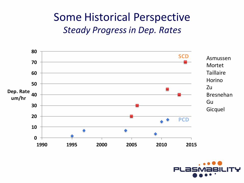
Some Historical PerspectiveSteady Progress in Dep. Rates
0
10
20
30
40
50
60
70
80
1990 1995 2000 2005 2010 2015
Dep. Rateum/hr
AsmussenMortetTaillaireHorinoZuBresnehanGuGicquel
SCD
PCD
Some Historical Perspective
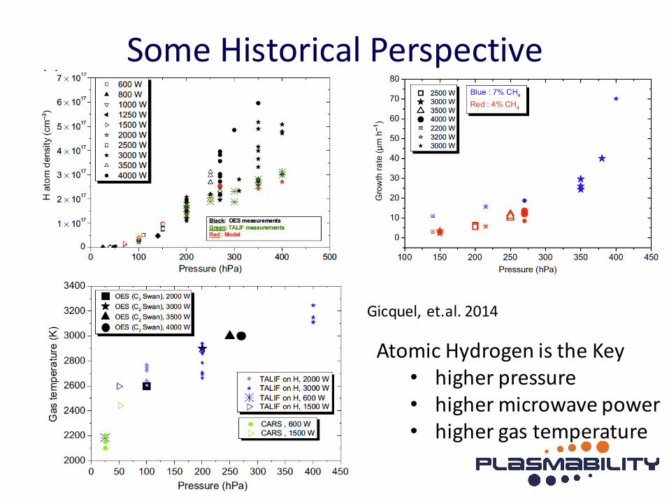
Gicquel, et.al. 2014
Atomic Hydrogen is the Key• higher pressure• higher microwave power• higher gas temperature
What This Means• To grow high quality diamond material at high rates the
following are needed:– high gas temperature to generate lot of atomic H
• for microwave systems this means high pressure and high microwave powers
– high quality vacuum practice• avoid nitrogen leaks and other impurities
– materials of construction that will not erode and cause contamination– careful temperature control of the sample
• Our program is to develop a reactor technology that will accomplish these goals at significantly lower cost and complexity.

Our Program• Develop an rf-‐based alternative to microwave plasma
diamond deposition reactors• Don't try to reinvent the physics -‐ aim for same power
densities, operating conditions, etc• Why might this be attractive ?
– rf power is much more energy efficient to product relative to microwave
– rf is more reliable and does not need maintenance (magnetron tube replacement for microwave)
– rf is much less bulky and more flexible to integrate– use may reduce overall costs significantly– rf is highly scalable in power

Goals of Initial Activity
• Investigate toroidal plasma as alternative to microwave • Assess how toroidal plasma operates in process range of
interest• Identify possible materials compatibility issues• Identify scaling possibilities• Understand capital cost components• Understand cost of ownership (dollars per carat)• Identify key application space
Toroidal Plasmas -‐ Background• Toroidal plasmas are used in semiconductor manufacturing
for generating large fluxes of atomic species– O, N, H, F, etc– CVD chamber clean– photoresist removal– surface oxide removal
• Power densities in the plasma 50+ W cm-‐3
• Gas temperatures >3000 C • Typical pressures 2-‐20 Torr• 400 kHz power – inexpensive, compact and highly reliable• 5 kW – 25 kW used today • scalable to higher powers

Toroidal Plasma Commercial Examples
MKS Instruments
Advanced Energy New Power Plasma
Semiconductor Manufacturing(over 40,000 installed)
Lighting
Sylvania
Why Toroidal Plasmas ?• It is very difficult to obtain the desired plasma conditions
using a simple rf discharge– 100+ W cm-‐3 volumetric power density desirable– 40-‐200 Torr gas pressure– 3000+ C gas temperature in discharge region
• Capacitively coupled systems will not have the the power density or gas temperature
• Inductively coupled systems may generate the power density, but typically only in a localized region near walls or antennas
• DC or rf plasma torches will have the requisite plasma conditions, but with difficulties related to contamination and wear
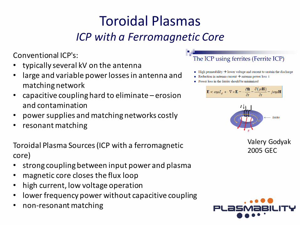
Toroidal PlasmasICP with a Ferromagnetic Core
Conventional ICP's:• typically several kV on the antenna• large and variable power losses in antenna and
matching network• capacitive coupling hard to eliminate – erosion
and contamination• power supplies and matching networks costly• resonant matching
Toroidal Plasma Sources (ICP with a ferromagnetic core)• strong coupling between input power and plasma• magnetic core closes the flux loop• high current, low voltage operation • lower frequency power without capacitive coupling• non-‐resonant matching
Valery Godyak2005 GEC
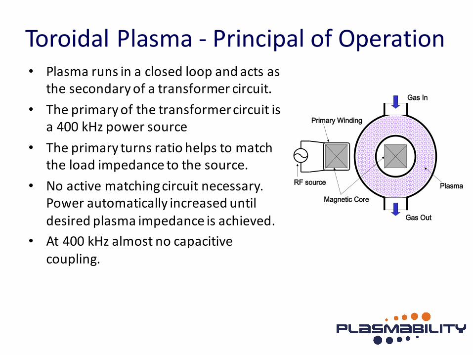
Toroidal Plasma -‐ Principal of Operation• Plasma runs in a closed loop and acts as
the secondary of a transformer circuit.• The primary of the transformer circuit is
a 400 kHz power source• The primary turns ratio helps to match
the load impedance to the source.• No active matching circuit necessary.
Power automatically increased until desired plasma impedance is achieved.
• At 400 kHz almost no capacitive coupling.
Gas In
Gas Out
Plasma
Magnetic Core
Primary Winding
RF source

Experimental Apparatus
process chambermagnetic cores

Polysilicon Results -‐ Raman
Ar: 1325 sccmH2: 250 sccmCH4: 10 sccmO2: 3.5 sccm30 Torr9.5 kW1030 C15 um/hr
500
1000
1500
2000
2500
3000
3500
4000
4500
5000
5500
800 900 1000 1100 1200 1300 1400 1500 1600 1700 1800
Intensity
cm-‐1
2/8/15
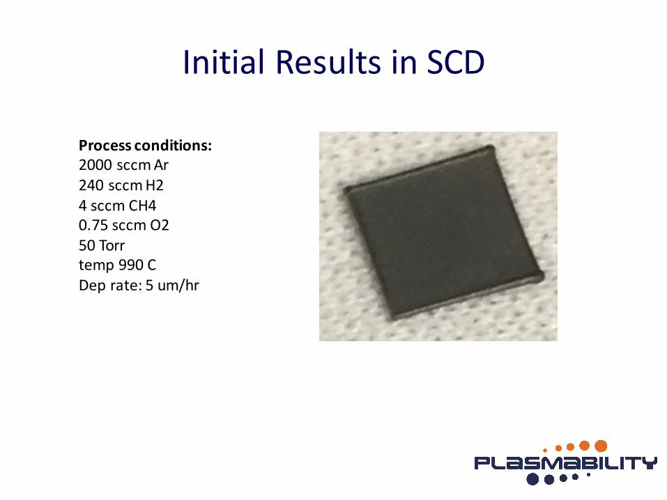
Initial Results in SCD
Process conditions:2000 sccmAr240 sccmH24 sccm CH40.75 sccm O250 Torrtemp 990 C Dep rate: 5 um/hr
What Have We Learned ?• Toroidal plasma design can generate plasma conditions similar
to that for microwave systems• Shape of plasma lends itself to unique process opportunities
– In principal can capture nearly 100% of the available reactant– For example, can coat inside and outside of tubular structures
• Highly scalable in power• Very compact source• Applications such as coating large silicon wafer maybe not
best choice for this technology• Initial deposition rates comparable to or greater than for
microwave reactors• Presence of argon does not seem to damage growing surface

Next Steps
• Further process development for both polycrystalline and single-‐crystal material
• Characterize high-‐capture sample holder

THANK YOU