transmission kikuchi diffraction in the scanning...
TRANSCRIPT
Robert Keller, Roy Geiss, Katherine Rice National Institute of Standards and Technology Nanoscale Reliability Group Boulder, Colorado USA [email protected]
Transmission Kikuchi Diffraction in the Scanning Electron Microscope
Acknowledgements Aimo Winkelmann – pattern simulations, physics insight. Daniel Goran – seeing the potential!
Outline
• The Challenge of Characterizing Nanomaterials • Conventional Electron Backscatter Diffraction (EBSD) • Transmission Kikuchi Diffraction, aka Transmission EBSD • The First TKD/t-EBSD Results • Electron Scattering and Sampling Volume • Conclusions
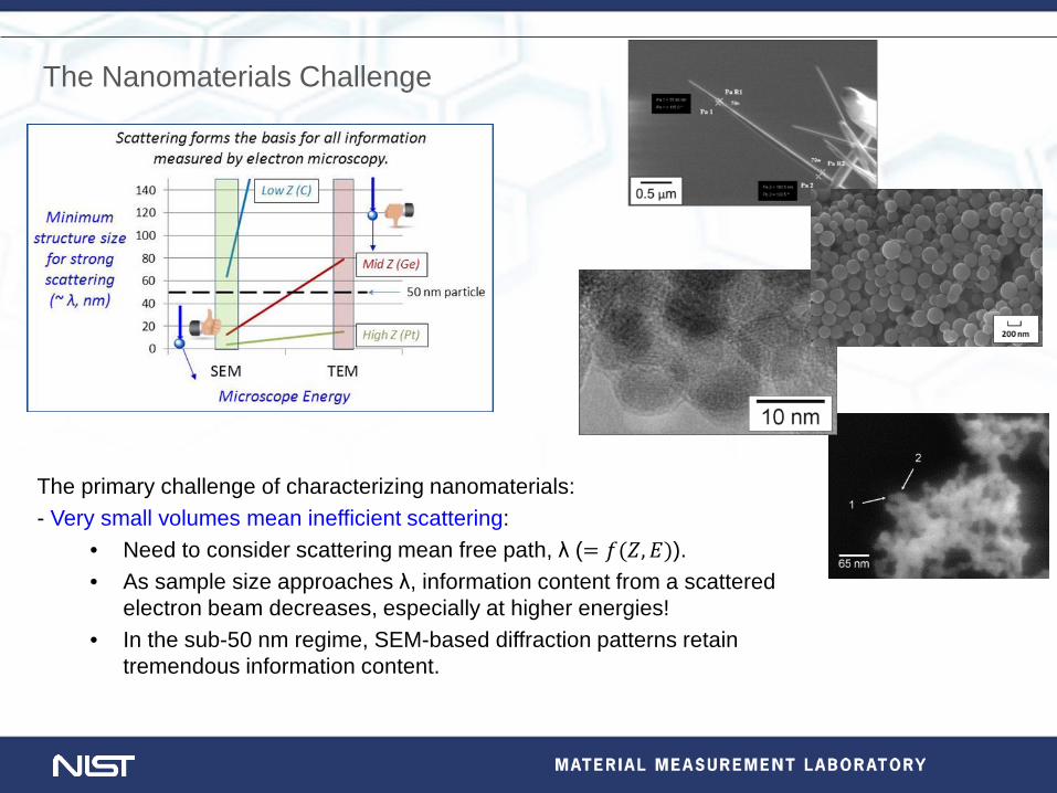
The Nanomaterials Challenge
The primary challenge of characterizing nanomaterials: - Very small volumes mean inefficient scattering:
• Need to consider scattering mean free path, λ (= 𝑓(𝑍,𝐸)). • As sample size approaches λ, information content from a scattered
electron beam decreases, especially at higher energies! • In the sub-50 nm regime, SEM-based diffraction patterns retain
tremendous information content.
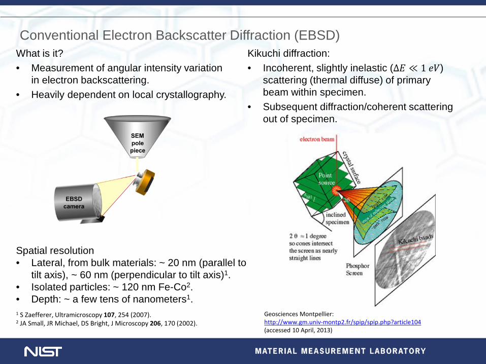
Conventional Electron Backscatter Diffraction (EBSD) What is it? • Measurement of angular intensity variation
in electron backscattering. • Heavily dependent on local crystallography.
Spatial resolution • Lateral, from bulk materials: ~ 20 nm (parallel to
tilt axis), ~ 60 nm (perpendicular to tilt axis)1. • Isolated particles: ~ 120 nm Fe-Co2. • Depth: ~ a few tens of nanometers1.
1 S Zaefferer, Ultramicroscopy 107, 254 (2007). 2 JA Small, JR Michael, DS Bright, J Microscopy 206, 170 (2002).
Geosciences Montpellier: http://www.gm.univ-montp2.fr/spip/spip.php?article104 (accessed 10 April, 2013)
Kikuchi diffraction: • Incoherent, slightly inelastic (∆𝐸 ≪ 1 𝑒𝑒)
scattering (thermal diffuse) of primary beam within specimen.
• Subsequent diffraction/coherent scattering out of specimen.
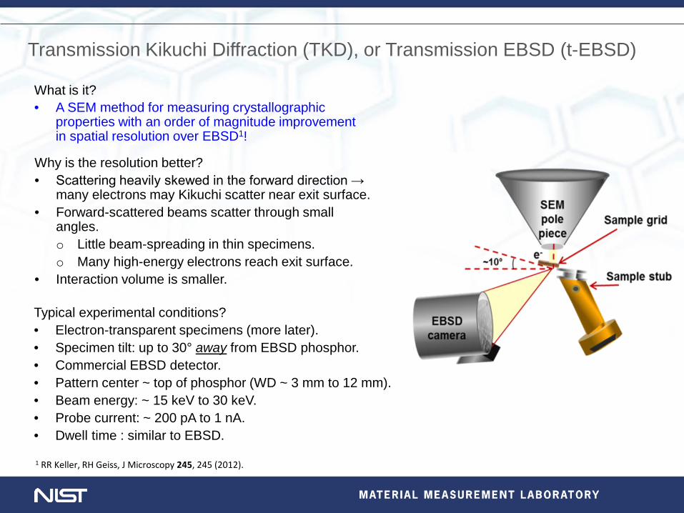
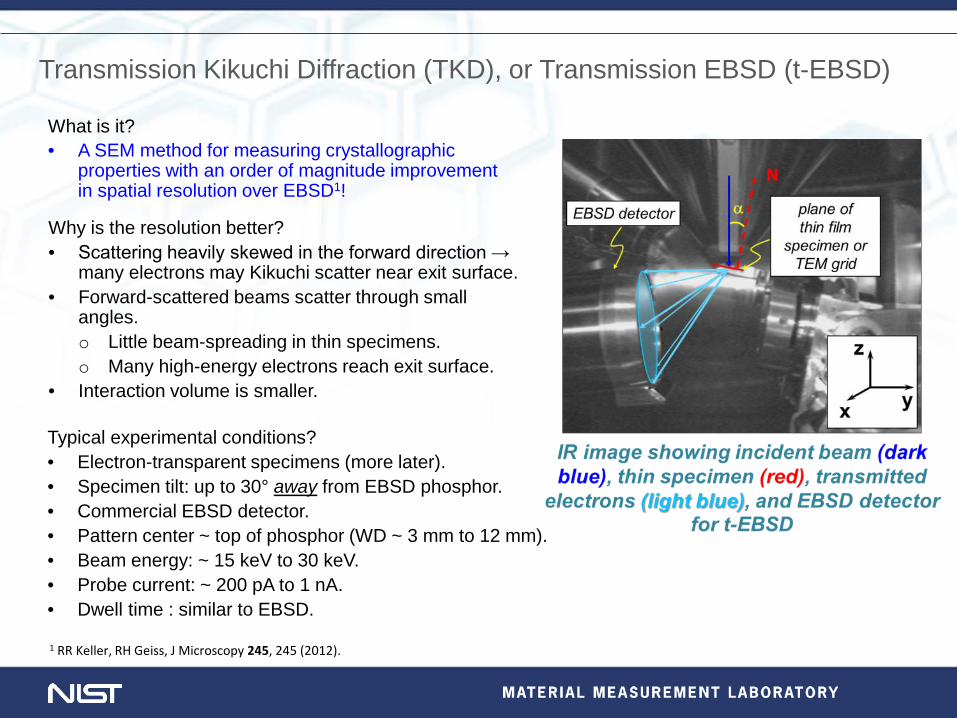
Transmission Kikuchi Diffraction (TKD), or Transmission EBSD (t-EBSD) What is it? • A SEM method for measuring crystallographic
properties with an order of magnitude improvement in spatial resolution over EBSD1!
1 RR Keller, RH Geiss, J Microscopy 245, 245 (2012).
Why is the resolution better? • Scattering heavily skewed in the forward direction →
many electrons may Kikuchi scatter near exit surface. • Forward-scattered beams scatter through small
angles. o Little beam-spreading in thin specimens. o Many high-energy electrons reach exit surface.
• Interaction volume is smaller.
Typical experimental conditions? • Electron-transparent specimens (more later). • Specimen tilt: up to 30° away from EBSD phosphor. • Commercial EBSD detector. • Pattern center ~ top of phosphor (WD ~ 3 mm to 12 mm). • Beam energy: ~ 15 keV to 30 keV. • Probe current: ~ 200 pA to 1 nA. • Dwell time : similar to EBSD.

Samples Any method that works for TEM sample preparation works for TKD/t-EBSD!
Positioning Sample Grids: • Simple – slip it under the end of a brass
clip attached to an SEM stub. • More involved – sacrifice an unused
TEM sample holder. Nanoparticles: • May be attached to TEM grids (with or
without support films) by placing a drop of a dilute solution containing the particles on it and allowing to dry.
Films and Foils: • May be deposited directly onto support
films in TEM grids that have nitride or oxide membranes suspended over etched Si windows.
• If free-standing, these may be adhered to a mesh-type TEM grid by a drop of silver paint or similar.
• Films on substrates: core drill, backside thin mechanically or chemically.

The First TKD/t-EBSD Results
GaN nanowires of diameter < 80 nm
Fe-Co particles of diameter < 15 nm
Particles (of Pt) as small as 2 nm have been studied by TKD/t-EBSD!
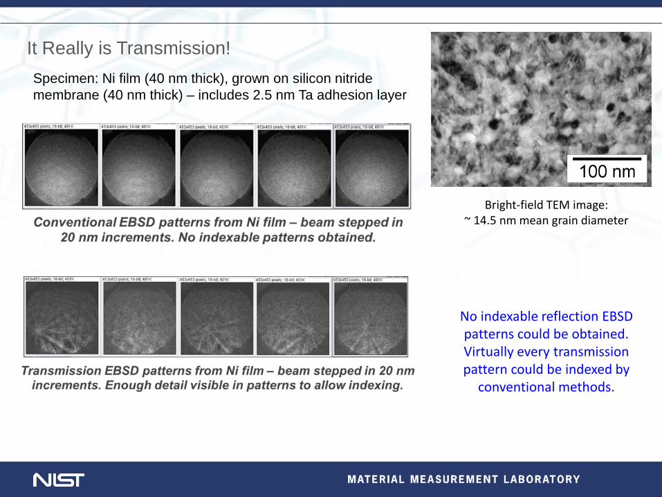
It Really is Transmission! Specimen: Ni film (40 nm thick), grown on silicon nitride membrane (40 nm thick) – includes 2.5 nm Ta adhesion layer
Bright-field TEM image: ~ 14.5 nm mean grain diameter
No indexable reflection EBSD patterns could be obtained. Virtually every transmission pattern could be indexed by
conventional methods.
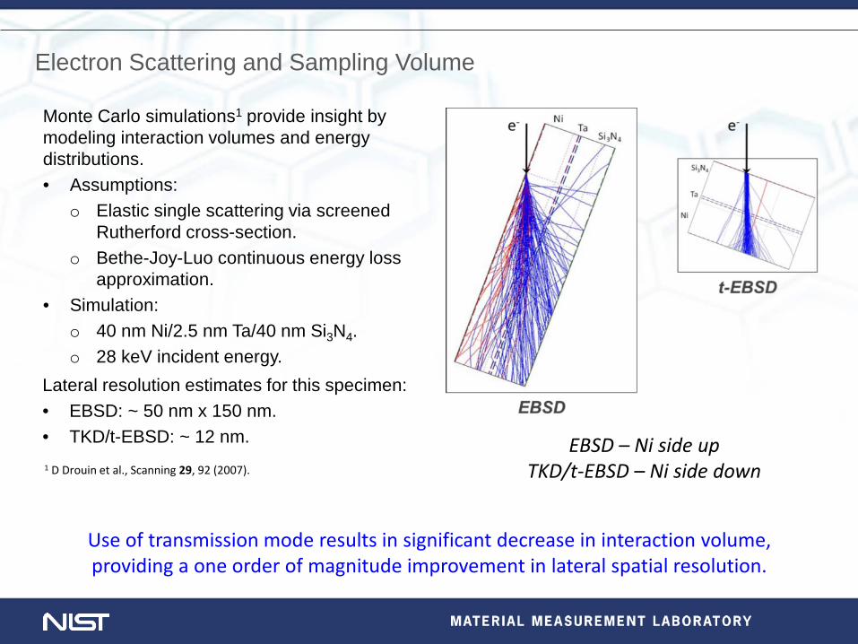
Electron Scattering and Sampling Volume Monte Carlo simulations1 provide insight by modeling interaction volumes and energy distributions. • Assumptions:
o Elastic single scattering via screened Rutherford cross-section.
o Bethe-Joy-Luo continuous energy loss approximation.
• Simulation: o 40 nm Ni/2.5 nm Ta/40 nm Si3N4. o 28 keV incident energy.
EBSD – Ni side up TKD/t-EBSD – Ni side down
Use of transmission mode results in significant decrease in interaction volume, providing a one order of magnitude improvement in lateral spatial resolution.
1 D Drouin et al., Scanning 29, 92 (2007).
Lateral resolution estimates for this specimen: • EBSD: ~ 50 nm x 150 nm. • TKD/t-EBSD: ~ 12 nm.

Where does the Important Signal come from?
Potential Kikuchi sources are everywhere in the specimen. But, to form a pattern, we need electrons that maintain coherence after diffraction.
10 nm Au/ 20 nm Si3N4
10 nm Au/ 50 nm Si3N4
Au film “up”
Au film “down”
Experiment: Au film on amorphous Si3N4 membranes
Electrons that diffract near the top surface cannot maintain coherence for a significant distance in the specimen → the most important Kikuchi scattering occurs near the exit surface.
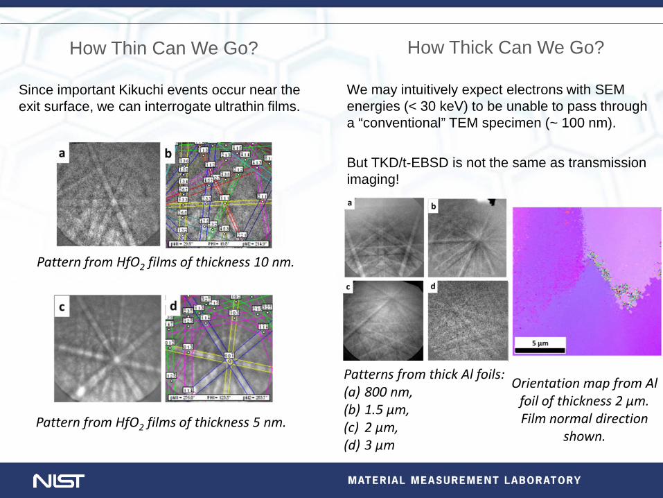
How Thin Can We Go?
Since important Kikuchi events occur near the exit surface, we can interrogate ultrathin films.
Patterns from thick Al foils: (a) 800 nm, (b) 1.5 µm, (c) 2 µm, (d) 3 µm
Pattern from HfO2 films of thickness 10 nm.
Pattern from HfO2 films of thickness 5 nm.
We may intuitively expect electrons with SEM energies (< 30 keV) to be unable to pass through a “conventional” TEM specimen (~ 100 nm). But TKD/t-EBSD is not the same as transmission imaging!
How Thick Can We Go?
Orientation map from Al foil of thickness 2 µm. Film normal direction
shown.
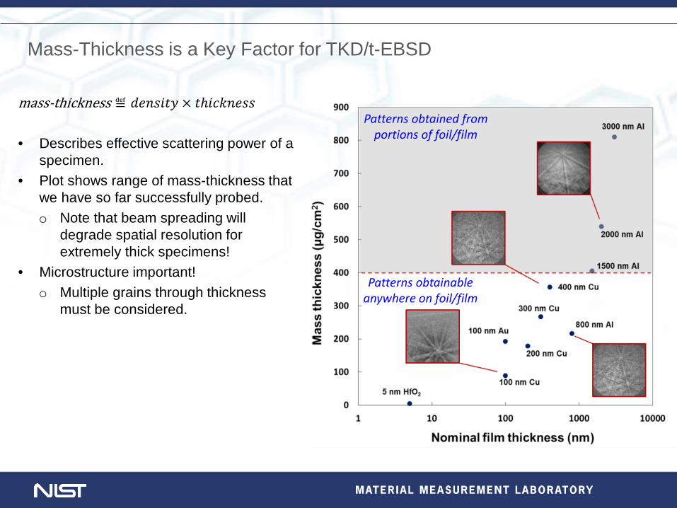
Mass-Thickness is a Key Factor for TKD/t-EBSD
mass-thickness ≝ 𝑑𝑒𝑑𝑑𝑑𝑑𝑑 × 𝑑𝑡𝑑𝑡𝑡𝑑𝑒𝑑𝑑 • Describes effective scattering power of a
specimen. • Plot shows range of mass-thickness that
we have so far successfully probed. o Note that beam spreading will
degrade spatial resolution for extremely thick specimens!
• Microstructure important! o Multiple grains through thickness
must be considered.
Patterns obtainable anywhere on foil/film
Patterns obtained from portions of foil/film

Conclusions – Transmission Kikuchi Diffraction/Transmission EBSD
Breakthrough measurement technology: • Lateral spatial resolution ~ single
nanometers – order of magnitude improvement over reflection EBSD!
• Isolated sub-10 nm nanoparticles. • Thinned bulk materials. Thick and thin: mass-thickness determines when TKD/t-EBSD may be effective. • Crystallographic properties from films of
thickness 5 nm to 3 μm. Can do it with commercial SEM and commercial EBSD – infrastructure in place!