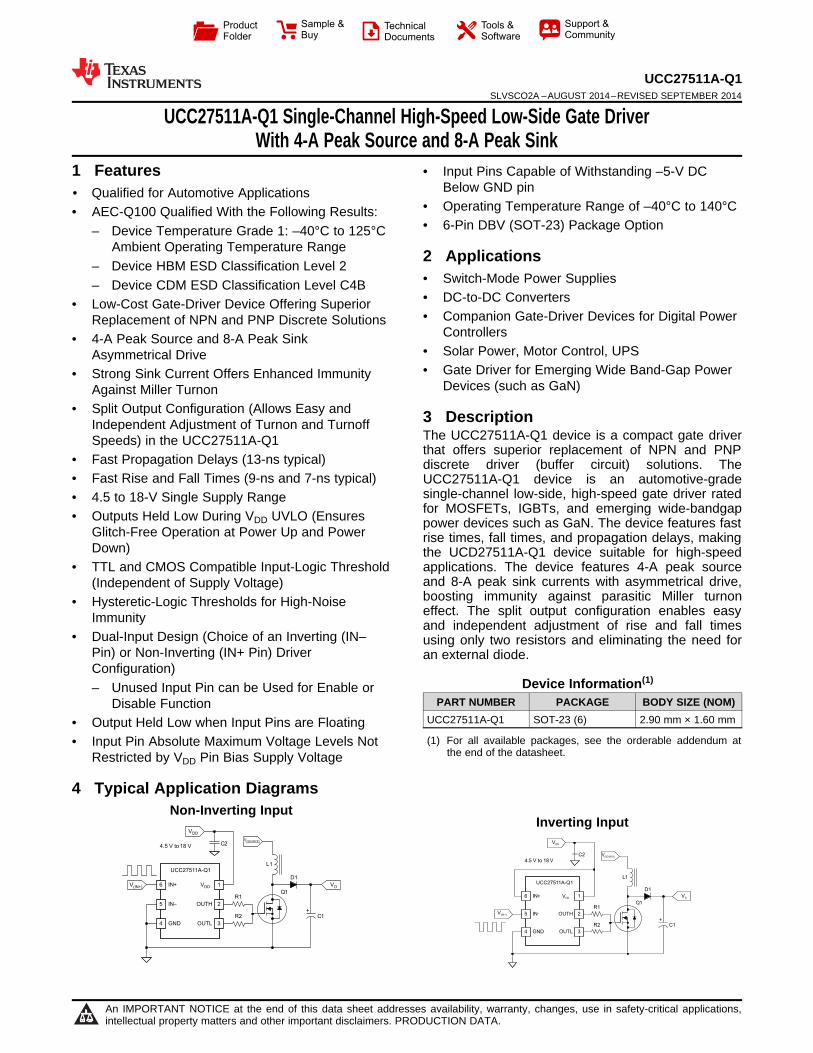
ucc27511a-q1 single-channel high-speed low … · 6 5 4 1 2 3 in+ in! gnd v dd outh outl r1 r2 q1 d...
TRANSCRIPT
6
5
4
1
2
3
IN+
IN–
GND
VDD
OUTH
OUTL
R1
R2
Q1
D1
C1+
L1
C24.5 V to 18 V
V(IN–)
VO
V(SOURCE)
VDD
UCC27511A-Q16
5
4
1
2
3
IN+
IN–
GND
VDD
OUTH
OUTL
UCC27511A-Q1
R1
R2
Q1
V(IN+)
D1
C1+
VO
V(SOURCE)
L1
C24.5 V to 18 V
VDD
Product
Folder
Sample &Buy
Technical
Documents
Tools &
Software
Support &Community
UCC27511A-Q1SLVSCO2A –AUGUST 2014–REVISED SEPTEMBER 2014
UCC27511A-Q1 Single-Channel High-Speed Low-Side Gate DriverWith 4-A Peak Source and 8-A Peak Sink
1 Features • Input Pins Capable of Withstanding –5-V DCBelow GND pin
1• Qualified for Automotive Applications• Operating Temperature Range of –40°C to 140°C• AEC-Q100 Qualified With the Following Results:• 6-Pin DBV (SOT-23) Package Option– Device Temperature Grade 1: –40°C to 125°C
Ambient Operating Temperature Range 2 Applications– Device HBM ESD Classification Level 2
• Switch-Mode Power Supplies– Device CDM ESD Classification Level C4B• DC-to-DC Converters• Low-Cost Gate-Driver Device Offering Superior• Companion Gate-Driver Devices for Digital PowerReplacement of NPN and PNP Discrete Solutions
Controllers• 4-A Peak Source and 8-A Peak Sink• Solar Power, Motor Control, UPSAsymmetrical Drive• Gate Driver for Emerging Wide Band-Gap Power• Strong Sink Current Offers Enhanced Immunity
Devices (such as GaN)Against Miller Turnon• Split Output Configuration (Allows Easy and 3 DescriptionIndependent Adjustment of Turnon and Turnoff
The UCC27511A-Q1 device is a compact gate driverSpeeds) in the UCC27511A-Q1that offers superior replacement of NPN and PNP
• Fast Propagation Delays (13-ns typical) discrete driver (buffer circuit) solutions. The• Fast Rise and Fall Times (9-ns and 7-ns typical) UCC27511A-Q1 device is an automotive-grade
single-channel low-side, high-speed gate driver rated• 4.5 to 18-V Single Supply Rangefor MOSFETs, IGBTs, and emerging wide-bandgap• Outputs Held Low During VDD UVLO (Ensures power devices such as GaN. The device features fast
Glitch-Free Operation at Power Up and Power rise times, fall times, and propagation delays, makingDown) the UCD27511A-Q1 device suitable for high-speed
• TTL and CMOS Compatible Input-Logic Threshold applications. The device features 4-A peak sourceand 8-A peak sink currents with asymmetrical drive,(Independent of Supply Voltage)boosting immunity against parasitic Miller turnon• Hysteretic-Logic Thresholds for High-Noiseeffect. The split output configuration enables easyImmunity and independent adjustment of rise and fall times
• Dual-Input Design (Choice of an Inverting (IN– using only two resistors and eliminating the need forPin) or Non-Inverting (IN+ Pin) Driver an external diode.Configuration)
Device Information(1)– Unused Input Pin can be Used for Enable or
PART NUMBER PACKAGE BODY SIZE (NOM)Disable FunctionUCC27511A-Q1 SOT-23 (6) 2.90 mm × 1.60 mm• Output Held Low when Input Pins are Floating(1) For all available packages, see the orderable addendum at• Input Pin Absolute Maximum Voltage Levels Not
the end of the datasheet.Restricted by VDD Pin Bias Supply Voltage
4 Typical Application DiagramsNon-Inverting Input
Inverting Input
1
An IMPORTANT NOTICE at the end of this data sheet addresses availability, warranty, changes, use in safety-critical applications,intellectual property matters and other important disclaimers. PRODUCTION DATA.

UCC27511A-Q1SLVSCO2A –AUGUST 2014–REVISED SEPTEMBER 2014 www.ti.com
Table of Contents8.2 Functional Block Diagram ....................................... 121 Features .................................................................. 18.3 Feature Description................................................. 122 Applications ........................................................... 18.4 Device Functional Modes........................................ 173 Description ............................................................. 1
9 Application and Implementation ........................ 184 Typical Application Diagrams .............................. 19.1 Application Information............................................ 185 Revision History..................................................... 29.2 Typical Application ................................................. 186 Pin Configuration and Functions ......................... 3
10 Power Supply Recommendations ..................... 227 Specifications......................................................... 411 Layout................................................................... 237.1 Absolute Maximum Ratings ...................................... 4
11.1 Layout Guidelines ................................................. 237.2 Handling Ratings....................................................... 411.2 Layout Example .................................................... 247.3 Recommended Operating Conditions....................... 4
12 Device and Documentation Support ................. 247.4 Thermal Information .................................................. 412.1 Trademarks ........................................................... 247.5 Electrical Characteristics........................................... 512.2 Electrostatic Discharge Caution............................ 247.6 Switching Characteristics .......................................... 612.3 Glossary ................................................................ 247.7 Typical Characteristics .............................................. 8
13 Mechanical, Packaging, and Orderable8 Detailed Description ............................................ 11Information ........................................................... 248.1 Overview ................................................................. 11
5 Revision History
Changes from Original (August 2014) to Revision A Page
• Changed the device status From: Product Preview To Production ....................................................................................... 1• Changed the ESD HBM Values From: MIN = -2000 V, MAX = 2000 V To: MIN = -4000 V, MAX = 4000 V ....................... 4
2 Submit Documentation Feedback Copyright © 2014, Texas Instruments Incorporated
Product Folder Links: UCC27511A-Q1

IN+
OUTH
OUTL
1
2
3
6
4
IN–5
GND
VDD
1
2
3
6
4
5
UCC27511A-Q1www.ti.com SLVSCO2A –AUGUST 2014–REVISED SEPTEMBER 2014
6 Pin Configuration and Functions
DBV Package6-Pin SOT-23
Top View
Pin FunctionsPIN I/O
FUNCTIONNO. NAME1 VDD I Bias supply input.
Sourcing current output of driver. Connect a resistor between the OUTH pin and the gate of the power-2 OUTH O switching device to adjust turnon speed.Sinking current output of driver. Connect a resistor between the OUTL pin and the gate of the power-3 OUTL O switching device to adjust turnoff speed.
4 GND — Ground. All signals referenced to this pin.Inverting input. When the driver is used in non-inverting configuration, connect the IN– pin to GND in5 IN– I order to enable output. The OUTx pin is held low if the IN– pin is unbiased or floating.Non-inverting input. When the driver is used in inverting configuration, connect the IN+ pin to VDD in6 IN+ I order to enable output. The OUTx pin is held low if the IN+ pin is unbiased or floating.
Copyright © 2014, Texas Instruments Incorporated Submit Documentation Feedback 3
Product Folder Links: UCC27511A-Q1

UCC27511A-Q1SLVSCO2A –AUGUST 2014–REVISED SEPTEMBER 2014 www.ti.com
7 Specifications
7.1 Absolute Maximum Ratings (1) (2) (3)
over operating free-air temperature range (unless otherwise noted)MIN MAX UNIT
Supply voltage VDD –0.3 20Input voltage IN+, IN– (4) –6 20
VDD +OUTH –0.3 V0.3Output voltage DC –0.3 20
OUTLRepetitive pulse less than 200 ns (5) –2 20
IO_DC (source) 0.3Output continuous current(OUTH source current and OUTL sink current) IO_DC (sink) 0.6
AIO_pulsed(source) 4Output pulsed current (0.5 µs)
(OUTH source current and OUTL sink current) IO_pulsed(sink) 8Operating virtual junction temperature range, TJ –40 150
Soldering, 10 sec. 300 °CLead temperature
Reflow 260
(1) Stresses beyond those listed under absolute maximum ratings may cause permanent damage to the device. These are stress ratingsonly and functional operation of the device at these or any other conditions beyond those indicated under recommended operatingconditions is not implied. Exposure to absolute-maximum-rated conditions for extended periods may affect device reliability.
(2) All voltages are with respect to GND unless otherwise noted. Currents are positive into and negative out of the specified terminal. Seethe Thermal Information section for thermal limitations and considerations of packages.
(3) These devices are sensitive to electrostatic discharge; follow proper device handling procedures.(4) Maximum voltage on input pins is not restricted by the voltage on the VDD pin.(5) Values are verified by characterization on bench.
7.2 Handling RatingsMIN MAX UNIT
Tstg Storage temperature range –65 150 °CHuman body model (HBM), per AEC Q100-002 (1) –4000 4000ElectrostaticV(ESD) Vdischarge Charged device model (CDM), per AEC Q100-011 –1000 1000
(1) AEC Q100-002 indicates HBM stressing is done in accordance with the ANSI/ESDA/JEDEC JS-001 specification.
7.3 Recommended Operating Conditionsover operating free-air temperature range (unless otherwise noted)
MIN NOM MAX UNITVDD Supply voltage 4.5 12 18 VVI Input voltage, IN+ and IN– –5 18 VTA Operating junction temperature range –40 140 °C
7.4 Thermal InformationDBV
THERMAL METRIC (1) UNIT6 PINS
RθJA Junction-to-ambient thermal resistance 217.8RθJC(top) Junction-to-case (top) thermal resistance 97.6RθJB Junction-to-board thermal resistance 72.2 °C/WψJT Junction-to-top characterization parameter 8.6ψJB Junction-to-board characterization parameter 71.6
(1) For more information about traditional and new thermal metrics, see the IC Package Thermal Metrics application report, SPRA953.
4 Submit Documentation Feedback Copyright © 2014, Texas Instruments Incorporated
Product Folder Links: UCC27511A-Q1

UCC27511A-Q1www.ti.com SLVSCO2A –AUGUST 2014–REVISED SEPTEMBER 2014
7.5 Electrical CharacteristicsVDD = 12 V, TA = TJ = –40°C to 140°C, 1-µF capacitor from VDD to GND. Currents are positive into, negative out of thespecified terminal.
PARAMETER TEST CONDITIONS MIN TYP MAX UNITBIAS CURRENTS
IN+ = VDD, IN– = GND 40 100 160I(START) Startup current VDD = 3.4 V IN+ = IN– = GND or IN+ = IN– = VDD 25 75 145 µA
IN+ = GND, IN– = VDD 20 60 115UNDERVOLTAGE LOCKOUT (UVLO)
TA = 25°C 3.91 4.2 4.5V(ON) Supply start threshold
TA = –40°C to 140°C 3.7 4.2 4.65VMinimum operating voltageV(OFF) 3.45 3.9 4.35after supply start
VDD(hys) Supply voltage hysteresis 0.2 0.3 0.5INPUTS (IN+, IN–)
Output high for IN+ pin,VIH(IN) Input signal high threshold 2.2 2.4Output low for IN– pinOutput low for IN+ pin, VVIL(IN) Input signal low threshold 1.0 1.2Output high for IN– pin
Vhys(IN) Input signal hysteresis 1SOURCE AND SINK CURRENTIP(SRC) Source peak current (1) C(LOAD) = 0.22 µF, ƒS = 1 kHz –4 AIP(SNK) Sink peak current (1) C(LOAD) = 0.22 µF, ƒS = 1 kHz 8 AOUTPUTS (OUTH, OUTL, OUT)
VDD = 12 V 50 90I(OUTH) = –10 mAVOH High output voltage
VDD = 4.5 V 60 130I(OUTH) = –10 mAmV
VDD = 12 5 6.5I(OUTL) = 10 mAVOL Low output voltage
VDD = 4.5 V 5.5 10I(OUTL) = 10 mAVDD = 12 V 5 7.5I(OUTH) = –10 mA
RO(H) Output pullup resistance (2)VDD = 4.5 V 5 11I(OUTH) = –10 mA
ΩVDD = 12 V 0.375 0.65I(OUTL) = 10 mA
RO(L) Output pulldown resistanceVDD = 4.5 V 0.45 0.75I(OUTL) = 10 mA
(1) Ensured by Design.(2) RO(H) represents the on-resistance of P-channel MOSFET in pullup structure of the output stage of the UCC27511A-Q1 device.
Copyright © 2014, Texas Instruments Incorporated Submit Documentation Feedback 5
Product Folder Links: UCC27511A-Q1
td(1)
Low
90%
10%
IN– pin
OUTPUT
High
INPUT
(IN+ pin)
Low
High
tr td(1) tr
UCC27511A-Q1SLVSCO2A –AUGUST 2014–REVISED SEPTEMBER 2014 www.ti.com
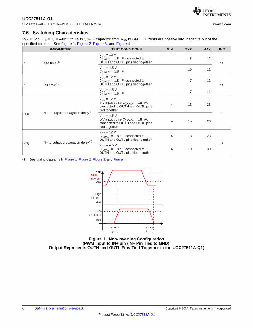
7.6 Switching CharacteristicsVDD = 12 V, TA = TJ = –40°C to 140°C, 1-µF capacitor from VDD to GND. Currents are positive into, negative out of thespecified terminal. See Figure 1, Figure 2, Figure 3, and Figure 4
PARAMETER TEST CONDITIONS MIN TYP MAX UNITVDD = 12 VC(LOAD) = 1.8 nF, connected to 8 12OUTH and OUTL pins tied togethertr Rise time (1) nsVDD = 4.5 V 16 22C(LOAD) = 1.8 nFVDD = 12 VC(LOAD) = 1.8 nF, connected to 7 11OUTH and OUTL pins tied togethertf Fall time (1) nsVDD = 4.5 V 7 11C(LOAD) = 1.8 nFVDD = 12 V5-V input pulse C(LOAD) = 1.8 nF, 4 13 23connected to OUTH and OUTL pinstied together
td(1) IN+ to output propagation delay (1) nsVDD = 4.5 V5-V input pulse C(LOAD) = 1.8 nF, 4 15 26connected to OUTH and OUTL pinstied togetherVDD = 12 VC(LOAD) = 1.8 nF, connected to 4 13 23OUTH and OUTL pins tied together
td(2) IN– to output propagation delay (1) nsVDD = 4.5 VC(LOAD) = 1.8 nF, connected to 4 19 30OUTH and OUTL pins tied together
(1) See timing diagrams in Figure 1, Figure 2, Figure 3, and Figure 4.
Figure 1. Non-Inverting Configuration(PWM Input to IN+ pin (IN– Pin Tied to GND),
Output Represents OUTH and OUTL Pins Tied Together in the UCC27511A-Q1)
6 Submit Documentation Feedback Copyright © 2014, Texas Instruments Incorporated
Product Folder Links: UCC27511A-Q1

td(2)
Low
90%
10%
ENABLE(IN– pin)
OUTPUT
High
INPUT
(IN+ pin)
Low
High
tr td(2) tr
td(1)
Low
90%
10%
ENABLE(IN+ pin)
OUTPUT
High
INPUT
(IN– pin)
Low
High
tr td(1) tr
td(2)
Low
90%
10%
IN+ pin
OUTPUT
High
INPUT
(IN– pin)
Low
High
tr td(2) tr
UCC27511A-Q1www.ti.com SLVSCO2A –AUGUST 2014–REVISED SEPTEMBER 2014
Figure 2. Inverting Configuration(PWM Input to IN– Pin (IN+ Pin Tied to VDD),
Output Represents OUTH and OUTL Pins Tied Together in the UCC27511A-Q1)
Figure 3. Enable And Disable Function Using IN+ Pin(Enable and Disable Signal Applied to IN+ Pin, PWM Input to IN– Pin,
Output Represents OUTH and OUTL Pins Tied Together in the UCC27511A-Q1)
Figure 4. Enable and Disable Function Using IN– Pin(Enable and Disable Signal Applied to IN– Pin, PWM Input to IN+ Pin,
Output Represents OUTH and OUTL Pins Tied Together in the UCC27511A-Q1)
Copyright © 2014, Texas Instruments Incorporated Submit Documentation Feedback 7
Product Folder Links: UCC27511A-Q1

1
1.5
2
2.5
3
3.5
−50 0 50 100 150
Temperature (°C)
Inp
utT
hre
sh
old
(V
)
Turn−On
Turn−Off
G014
4
5
6
7
8
−50 0 50 100 150
Temperature (°C)
Outp
ut P
ullu
p R
esis
tance (
W)
RO(H)
G004
0.1
0.2
0.3
0.4
0.5
−50 0 50 100 150
Temperature (°C)
Op
era
tin
g S
up
ply
Cu
rre
nt
(mA
) IN+ = Low, IN– = Low
IN+ = High, IN– = Low
G002
3.6
3.8
4
4.2
4.4
4.6
−50 0 50 100 150
Temperature (°C)
UV
LO
Th
resh
old
(V
)UVLO Rising
UVLO Falling
G003
0.05
0.06
0.07
0.08
0.09
0.1
0.11
0.12
−50 0 50 100 150
Temperature (°C)
Sta
rtu
p C
urr
en
t (m
A)
IN+ = Low, IN– = Low
IN+ = High, IN– = Low
G001
2
2.5
3
3.5
4
−50 0 50 100 150
Temperature (°C)
Su
pp
ly C
urr
en
t (m
A)
G013
UCC27511A-Q1SLVSCO2A –AUGUST 2014–REVISED SEPTEMBER 2014 www.ti.com
7.7 Typical Characteristics
VDD = 3.4 V VDD = 12 V C(LOAD) = 500 pF ƒS = 500 kHz
Figure 5. Startup Current vs Temperature Figure 6. Operating Supply Current vs Temperature (OutputSwitching)
VDD = 12 V
Figure 7. Supply Current vs Temperature (Output in DC On Figure 8. UVLO Threshold Voltage vs Temperatureor Off Condition)
VDD = 12 V C(LOAD) = 1.8 nF VDD = 12 V IO = 10 mA
Figure 9. Input Threshold vs Temperature Figure 10. Output Pullup Resistance vs Temperature
8 Submit Documentation Feedback Copyright © 2014, Texas Instruments Incorporated
Product Folder Links: UCC27511A-Q1

0
2
4
6
8
10
12
14
16
18
20
0 100 200 300 400 500 600 700
Frequency (kHz)
Su
pp
ly C
urr
en
t (m
A)
V = 4.5 VDD
V = 12 VDD
V = 15 VDD
G010
6
8
10
12
14
16
18
20
0 4 8 12 16 20
Supply Voltage (V)
Pro
pa
ga
tio
n D
ela
y (
ns)
Turn−On
Turn−Off
G007
6
7
8
9
10
−50 0 50 100 150
Temperature (°C)
Fa
llT
ime
(n
s)
G000
5
10
15
20
−50 0 50 100 150
Temperature (°C)
Pro
pa
ga
tio
n D
ela
y (
ns)
Turn−On
Turn−Off
G006
0.1
0.3
0.5
0.7
0.8
−50 0 50 100 150
Temperature (°C)
Outp
ut P
ulld
ow
n R
esis
tance (
W)
RO(L)
G005
4
5
6
7
8
−50 0 50 100 150
Temperature (°C)
Ris
eT
ime
(n
s)
G000
UCC27511A-Q1www.ti.com SLVSCO2A –AUGUST 2014–REVISED SEPTEMBER 2014
Typical Characteristics (continued)
VDD = 12 V IO = 10 mA VDD = 12 V C(LOAD) = 1.8 nF
Figure 11. Output Pull-Down Resistance vs Temperature Figure 12. Rise Time vs Temperature
VDD = 12 V C(LOAD) = 1.8 nF VDD = 12 V
Figure 13. Fall Time vs Temperature Figure 14. Input to Output Propagation Delay vsTemperature
C(LOAD) = 1.8 nF
Figure 15. Operating Supply Current vs Frequency Figure 16. Propagation Delays vs Supply Voltage
Copyright © 2014, Texas Instruments Incorporated Submit Documentation Feedback 9
Product Folder Links: UCC27511A-Q1

5
10
15
20
0 4 8 12 16 20
Supply Voltage (V)
Ris
eT
ime
(n
s)
G008
2
4
6
8
10
0 4 8 12 16 20
Supply Voltage (V)
Fa
llT
ime
(n
s)
G009
UCC27511A-Q1SLVSCO2A –AUGUST 2014–REVISED SEPTEMBER 2014 www.ti.com
Typical Characteristics (continued)
Figure 17. Rise Time vs Supply Voltage Figure 18. Fall Time vs Supply Voltage
10 Submit Documentation Feedback Copyright © 2014, Texas Instruments Incorporated
Product Folder Links: UCC27511A-Q1
UCC27511A-Q1www.ti.com SLVSCO2A –AUGUST 2014–REVISED SEPTEMBER 2014
8 Detailed Description
8.1 OverviewThe UCC27511A-Q1 single-channel high-speed low-side gate-driver device is capable of effectively drivingMOSFET and IGBT power switches. Using a design that inherently minimizes shoot-through current, theUCC27511A-Q1 device is capable of sourcing and sinking high peak-current pulses into capacitive loads offeringrail-to-rail drive capability and extremely small propagation delay of 13 ns (typical).
The UCC27511A-Q1 device provides 4-A source, 8-A sink (asymmetrical drive) peak-drive current capability.Strong sink capability in asymmetrical drive boosts immunity against parasitic, Miller turnon effect. TheUCC27511A-Q1 device also features a unique split output configuration where the gate-drive current is sourcedthrough the OUTH pin and sunk through the OUTL pin. This unique pin arrangement allows the user to applyindependent turnon and turnoff resistors to the OUTH and OUTL pins (respectively) and easily control theswitching slew rates.
Alternatively the OUTH and OUTL pins can be tied together, which results in a typical gate driver outputconfiguration where the source and sink currents are delivered from the same pin. In case of UCC27511A-Q1device, the state of the device's output is simply determined by the combined states of the OUTH and OUTL pinswhen tied together. Output high implies that OUTH pin is pulled close to VDD pin bias voltage while OUTL pin isin high-impedance state. Similarly output low implies that OUTL pin is pulled close to the GND pin while OUTHpin is in high-impedance state. OUTH pulled to VDD, while OUTL pulled to GND pin simultaneously is not a validstate for the device.
The UCC27511A-Q1 device is designed to operate over a wide VDD range of 4.5 to 18 V and wide temperaturerange of –40°C to 140°C. Internal undervoltage lockout (UVLO) circuitry on the VDD pin holds the output lowoutside VDD operating range. The capability to operate at low voltage levels, such as below 5 V, along with best-in-class switching characteristics, is especially suited for driving emerging wide band-gap power-switchingdevices such as GaN power-semiconductor devices.
The UCC27511A-Q1 device features a dual-input design which offers flexibility of implementing both inverting(IN– pin) and non-inverting (IN+ pin) configuration with the same device. Either the IN+ or IN– pin can be used tocontrol the state of the driver output. The unused input pin can be used for enable and disable functions. Forsystem robustness, internal pullup and pulldown resistors on the input pins ensure that outputs are held lowwhen the input pins are in floating condition. Therefore the unused input pin is not left floating and must beproperly biased to ensure that driver output is in enabled for normal operation.
The input pin threshold of the UCC27511A-Q1 device is based on TTL and CMOS-compatible low-voltage logicwhich is fixed and independent of the VDD supply voltage. Wide hysteresis between the high and low thresholdsoffers excellent noise immunity.
Table 1. UCC27511A-Q1 Device SummaryPART NUMBER PACKAGE PEAK CURRENT (SOURCE, INPUT THRESHOLD LOGICSINK)
UCC27511A-Q1DBV SOT-23, 6 pin CMOS/TTL-Compatible4-A, 8-A (low voltage, independent of VDD(Asymmetrical Drive) bias voltage)
Copyright © 2014, Texas Instruments Incorporated Submit Documentation Feedback 11
Product Folder Links: UCC27511A-Q1

6
5
4
1
2
3
200 kΩ
VDD
230 kΩ
UVLO
VDD
VDD
VDD
OUTH
OUTL
IN+
IN–
GND
UCC27511A-Q1SLVSCO2A –AUGUST 2014–REVISED SEPTEMBER 2014 www.ti.com
Table 2. UCC27511A-Q1 Features and BenefitsFEATURE BENEFIT
High current capability offers flexibility in employing UCC2751xHigh source and sink current capability family of devices to drive a variety of power switching devices at4 A and 8 A (Asymmetrical) – UCC27511A-Q1 device varying speedsbest-in-class 13-ns (typ) propagation delay Extremely low pulse-transmission distortionExpanded VDD Operating range of 4.5 V to 18 V Flexibility in system design
Low VDD operation ensures compatibility with emerging wide band-Expanded operating temperature range of –40°C to 140°Cgap power devices such as GaN(See the Electrical Characteristics table)Outputs are held low in UVLO condition, which ensures predictableVDD UVLO Protection glitch-free operation at power up and power downEnables the device to pass abnormal-condition system tests andOutputs held low when input pins (INx) in floating condition delivers robust operation
Ability of input pins (and enable pin in UCC27518/9) to handle System simplification, especially related to auxiliary bias supplyvoltage levels not restricted by VDD pin bias voltage architectureSplit output structure in the UCC27511A-Q1 device (OUTH, OUTL) Allows independent optimization of turnon and turnoff speedsStrong sink current (8 A) and low pulldown impedance (0.375 Ω) in High immunity to C x dV/dt Miller turnon eventsthe UCC27511A-Q1 device
Enhanced noise immunity, while retaining compatibility withCMOS/TTL compatible input-threshold logic with wide hysteresis in microcontroller logic-level input signals (3.3 V, 5 V) optimized forthe UCC27511A-Q1 device digital power
8.2 Functional Block Diagram
8.3 Feature DescriptionIn the following sections, the term output, or OUT refers to the combined state that results when the OUTH pin istied directly to the OUTL pin. As stated earlier, output high, or OUT high refers to the state when the OUTH pin ispulled close to VDD pin bias voltage while the OUTL pin is in high-impedance state. Similarly output low or OUTlow implies that the OUTL pin is pulled close to the GND pin while the OUTH pin is in high-impedance state.
8.3.1 VDD and Undervoltage LockoutThe UCC27511A-Q1 device has and internal undervoltage-lockout (UVLO) protection feature on the VDD pinsupply circuit blocks. Whenever the driver is in UVLO condition (for example when the VDD voltage is less thanV(ON) during power up and when the VDD voltage is less than V(OFF) during power down), this circuit holds alloutputs low, regardless of the status of the inputs. The UVLO is typically 4.2 V with 300-mV typical hysteresis.This hysteresis prevents chatter when low VDD supply voltages have noise from the power supply and also whenthere are droops in the VDD bias voltage when the system commences switching and a sudden increase in IDDoccurs. The capability to operate at low voltage levels such as below 5 V, along with best-in-class switchingcharacteristics, is especially suited for driving emerging GaN wide band-gap power-semiconductor devices.
12 Submit Documentation Feedback Copyright © 2014, Texas Instruments Incorporated
Product Folder Links: UCC27511A-Q1
VDD
ThresholdVDD
IN+
OUTx
IN–
VDD
Threshold
IN–
OUTx
IN+
UCC27511A-Q1www.ti.com SLVSCO2A –AUGUST 2014–REVISED SEPTEMBER 2014
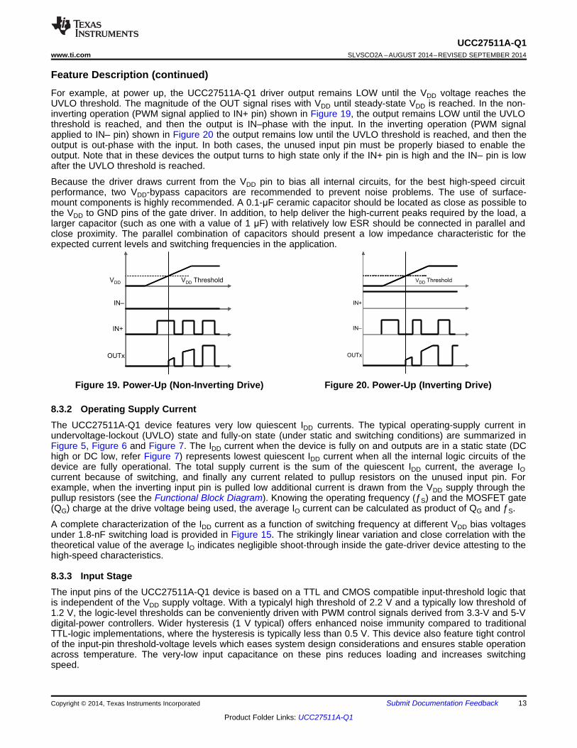
Feature Description (continued)For example, at power up, the UCC27511A-Q1 driver output remains LOW until the VDD voltage reaches theUVLO threshold. The magnitude of the OUT signal rises with VDD until steady-state VDD is reached. In the non-inverting operation (PWM signal applied to IN+ pin) shown in Figure 19, the output remains LOW until the UVLOthreshold is reached, and then the output is IN–phase with the input. In the inverting operation (PWM signalapplied to IN– pin) shown in Figure 20 the output remains low until the UVLO threshold is reached, and then theoutput is out-phase with the input. In both cases, the unused input pin must be properly biased to enable theoutput. Note that in these devices the output turns to high state only if the IN+ pin is high and the IN– pin is lowafter the UVLO threshold is reached.
Because the driver draws current from the VDD pin to bias all internal circuits, for the best high-speed circuitperformance, two VDD-bypass capacitors are recommended to prevent noise problems. The use of surface-mount components is highly recommended. A 0.1-μF ceramic capacitor should be located as close as possible tothe VDD to GND pins of the gate driver. In addition, to help deliver the high-current peaks required by the load, alarger capacitor (such as one with a value of 1 μF) with relatively low ESR should be connected in parallel andclose proximity. The parallel combination of capacitors should present a low impedance characteristic for theexpected current levels and switching frequencies in the application.
Figure 19. Power-Up (Non-Inverting Drive) Figure 20. Power-Up (Inverting Drive)
8.3.2 Operating Supply CurrentThe UCC27511A-Q1 device features very low quiescent IDD currents. The typical operating-supply current inundervoltage-lockout (UVLO) state and fully-on state (under static and switching conditions) are summarized inFigure 5, Figure 6 and Figure 7. The IDD current when the device is fully on and outputs are in a static state (DChigh or DC low, refer Figure 7) represents lowest quiescent IDD current when all the internal logic circuits of thedevice are fully operational. The total supply current is the sum of the quiescent IDD current, the average IOcurrent because of switching, and finally any current related to pullup resistors on the unused input pin. Forexample, when the inverting input pin is pulled low additional current is drawn from the VDD supply through thepullup resistors (see the Functional Block Diagram). Knowing the operating frequency (ƒS) and the MOSFET gate(QG) charge at the drive voltage being used, the average IO current can be calculated as product of QG and ƒS.
A complete characterization of the IDD current as a function of switching frequency at different VDD bias voltagesunder 1.8-nF switching load is provided in Figure 15. The strikingly linear variation and close correlation with thetheoretical value of the average IO indicates negligible shoot-through inside the gate-driver device attesting to thehigh-speed characteristics.
8.3.3 Input StageThe input pins of the UCC27511A-Q1 device is based on a TTL and CMOS compatible input-threshold logic thatis independent of the VDD supply voltage. With a typicalyl high threshold of 2.2 V and a typically low threshold of1.2 V, the logic-level thresholds can be conveniently driven with PWM control signals derived from 3.3-V and 5-Vdigital-power controllers. Wider hysteresis (1 V typical) offers enhanced noise immunity compared to traditionalTTL-logic implementations, where the hysteresis is typically less than 0.5 V. This device also feature tight controlof the input-pin threshold-voltage levels which eases system design considerations and ensures stable operationacross temperature. The very-low input capacitance on these pins reduces loading and increases switchingspeed.
Copyright © 2014, Texas Instruments Incorporated Submit Documentation Feedback 13
Product Folder Links: UCC27511A-Q1

UCC27511A-Q1SLVSCO2A –AUGUST 2014–REVISED SEPTEMBER 2014 www.ti.com
Feature Description (continued)Whenever any of the input pins are in a floating condition, the output of the respective channel is held in the lowstate. This function is achieved using VDD-pullup resistors on all the inverting inputs (IN– pin) or GND-pulldownresistors on all the non-inverting input pins (IN+ pin), (see the Functional Block Diagram).
The device also features a dual-input configuration with two input pins available to control the state of the output.The user has the flexibility to drive the device using either a non-inverting input pin (IN+) or an inverting input pin(IN–). The state of the output pin is dependent on the bias on both the IN+ and IN– pins. For additionalclarification, refer to the I/O-logic truth table (Table 3) and the typical application diagrams, (Figure 22 andFigure 23).
When an input pin is selected for PWM drive, the other input pin (the unused input pin) must be properly biasedin order to enable the output. As previously stated, the unused input pin cannot remain in a floating conditionbecause whenever any input pin is left in a floating condition the output is disabled. Alternatively, the unusedinput pin can effectively be used to implement an enable or disable function. The following explains this function:• In order to drive the device in a non-inverting configuration, apply the PWM-control input signal to IN+ pin. In
this case, the unused input pin, IN–, must be biased low (such as tied to GND) in order to enable the output.– Alternately, the IN– pin is used to implement the enable or disable function using an external logic signal.
OUT is disabled when IN– is biased high and OUT is enabled when IN– is biased low.• In order to drive the device in an inverting configuration, apply the PWM-control input signal to IN– pin. In this
case, the unused input pin, IN+, must be biased high (such as tied to VDD) in order to enable the output.– Alternately, the IN+ pin is used to implement the enable or disable function using an external logic signal.
OUT is disabled when IN+ is biased low and OUT is enabled when IN+ is biased high.• Finally, note that the output pin can be driven into a high state only when the IN+ pin is biased high and the
IN– input is biased low.
The input stage of the driver is preferably driven by a signal with a short rise or fall time. Use caution wheneverthe driver is used with slowly varying input signals, especially in situations where the device is located in amechanical socket or PCB layout that is not optimal:• High dI/dt current from the driver output coupled with board layout parasitics can cause ground bounce. The
differential voltage between input pins and GND is modified and triggers an unintended change of outputstate because of fast 13-ns propagation delay which can ultimately result in high-frequency oscillations thatincrease power dissipation and pose a risk of damage to the device.
• A 1-V input-threshold hysteresis boosts noise immunity compared to most other industry standard drivers.• In the worst case, when a slow input signal is used and PCB layout is not optimal, adding a small capacitor (1
nF) between the input pin and GND pin very close to the driver device may be necessary which helps toconvert the differential mode noise with respect to the input-logic circuitry into common-mode noise and avoidunintended change of output state.
If limiting the rise or fall times to the power device is the primary goal, then an external resistance is highlyrecommended between the output of the driver and the power device instead of adding delays on the inputsignal. This external resistor has the additional benefit of reducing part of the gate-charge related powerdissipation in the gate-driver device package and transferring the power dissipation into the external resistor.
8.3.4 Enable FunctionAs mentioned earlier, an enable and disable function is easily implemented in UCC27511A-Q1 device using theunused input pin. When the IN+ pin is pulled down to GND or the IN– pin is pulled down to VDD, the output isdisabled. Thus the IN+ pin can be used like an enable pin that is based on active-high logic, while the IN– pincan be used like an enable pin that is based on active-low logic.
8.3.5 Output StageFigure 21 shows the output stage of the UCC27511A-Q1 device. The UCC27511A-Q1 device features a uniquearchitecture on the output stage which delivers the highest peak-source current when the peak source current ismost needed during the Miller plateau region of the power switch turnon transition (when the power-switch drainor collector voltage experiences dV/dt). The device output stage features a hybrid pullup structure using aparallel arrangement of N-channel and P-channel MOSFET devices. By turning on the N-channel MOSFETduring a narrow instant when the output changes state from low to high, the gate-driver device is able to deliver abrief boost in the peak-sourcing current enabling fast turnon.
14 Submit Documentation Feedback Copyright © 2014, Texas Instruments Incorporated
Product Folder Links: UCC27511A-Q1
6
5
4
1
2
3
IN+
IN–
GND
VDD
OUTH
OUTL
UCC27511A-Q1
R1
R2
Q1
V(IN+)
D1
C1+
VO
V(SOURCE)
L1
C24.5 V to 18 V
VDD
VDD
RO(H)
RO(L)
Gate
voltage
boost
Narrow pulse at
each turn on
Anti shoot-
through
circuitry
Input signal
Pullup
R(NMOS)
OUTL
OUTH
UCC27511A-Q1www.ti.com SLVSCO2A –AUGUST 2014–REVISED SEPTEMBER 2014
Feature Description (continued)
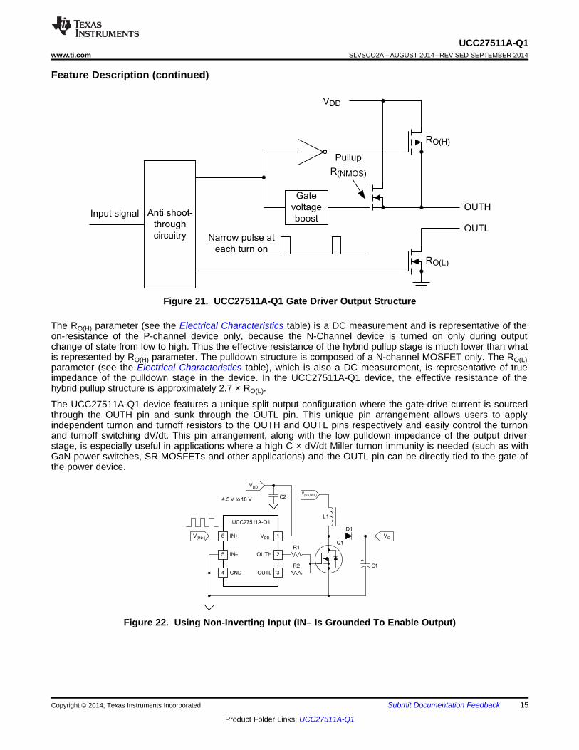
Figure 21. UCC27511A-Q1 Gate Driver Output Structure
The RO(H) parameter (see the Electrical Characteristics table) is a DC measurement and is representative of theon-resistance of the P-channel device only, because the N-Channel device is turned on only during outputchange of state from low to high. Thus the effective resistance of the hybrid pullup stage is much lower than whatis represented by RO(H) parameter. The pulldown structure is composed of a N-channel MOSFET only. The RO(L)parameter (see the Electrical Characteristics table), which is also a DC measurement, is representative of trueimpedance of the pulldown stage in the device. In the UCC27511A-Q1 device, the effective resistance of thehybrid pullup structure is approximately 2.7 × RO(L).
The UCC27511A-Q1 device features a unique split output configuration where the gate-drive current is sourcedthrough the OUTH pin and sunk through the OUTL pin. This unique pin arrangement allows users to applyindependent turnon and turnoff resistors to the OUTH and OUTL pins respectively and easily control the turnonand turnoff switching dV/dt. This pin arrangement, along with the low pulldown impedance of the output driverstage, is especially useful in applications where a high C × dV/dt Miller turnon immunity is needed (such as withGaN power switches, SR MOSFETs and other applications) and the OUTL pin can be directly tied to the gate ofthe power device.
Figure 22. Using Non-Inverting Input (IN– Is Grounded To Enable Output)
Copyright © 2014, Texas Instruments Incorporated Submit Documentation Feedback 15
Product Folder Links: UCC27511A-Q1
Gate Driver
RO(L)
RG
C(GD)
C(GS)
C(OSS)
VDS
I(SNK)
VI
VTH
ON OFF
Miller Turn-On Spike in VGS
VDS of
MOSFET
VGS of
MOSFET
OUTL
(of MOSFET)
6
5
4
1
2
3
IN+
IN–
GND
VDD
OUTH
OUTL
R1
R2
Q1
D1
C1+
L1
C24.5 V to 18 V
V(IN–)
VO
V(SOURCE)
VDD
UCC27511A-Q1
UCC27511A-Q1SLVSCO2A –AUGUST 2014–REVISED SEPTEMBER 2014 www.ti.com
Feature Description (continued)
Figure 23. Using Inverting Input (IN+ Is Tied To VDD Enable Output)
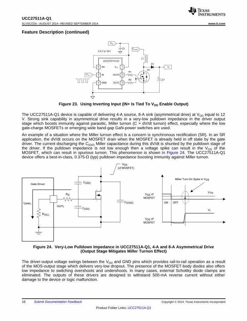
The UCC27511A-Q1 device is capable of delivering 4-A source, 8-A sink (asymmetrical drive) at VDD equal to 12V. Strong sink capability in asymmetrical drive results in a very-low pulldown impedance in the driver outputstage which boosts immunity against parasitic, Miller turnon (C × dV/dt turnon) effect, especially where the lowgate-charge MOSFETs or emerging wide band-gap GaN-power switches are used.
An example of a situation where the Miller turnon effect is a concern is synchronous rectification (SR). In an SRapplication, the dV/dt occurs on the MOSFET drain when the MOSFET is already held in off state by the gatedriver. The current discharging the C(GD) Miller capacitance during this dV/dt is shunted by the pulldown stage ofthe driver. If the pulldown impedance is not low enough then a voltage spike can result in the VGS of theMOSFET, which can result in spurious turnon. This phenomenon is shown in Figure 24. The UCC27511A-Q1device offers a best-in-class, 0.375-Ω (typ) pulldown impedance boosting immunity against Miller turnon.
Figure 24. Very-Low Pulldown Impedance in UCC27511A-Q1, 4-A and 8-A Asymmetrical Drive(Output Stage Mitigates Miller Turnon Effect)
The driver-output voltage swings between the VDD and GND pins which provides rail-to-rail operation as a resultof the MOS-output stage which delivers very-low dropout. The presence of the MOSFET-body diodes also offerslow impedance to switching overshoots and undershoots. In many cases, external Schottky diode clamps areeliminated. The outputs of these drivers are designed to withstand 500-mA reverse current without eitherdamage to the device or logic malfunction.
16 Submit Documentation Feedback Copyright © 2014, Texas Instruments Incorporated
Product Folder Links: UCC27511A-Q1
UCC27511A-Q1www.ti.com SLVSCO2A –AUGUST 2014–REVISED SEPTEMBER 2014
Feature Description (continued)8.3.6 Low Propagation DelaysThe UCC27511A-Q1 driver device features best-in-class input-to-output propagation delay of 13 ns (typical) atVDD equal to 12 V, which promises the lowest level of pulse transmission distortion available from industry-standard gate-driver devices for high-frequency switching applications. As shown in Figure 14, very little variationin propagation delay occurs with temperature and supply voltage, offering typically less than 20-ns propagationdelays across the entire range of application conditions.
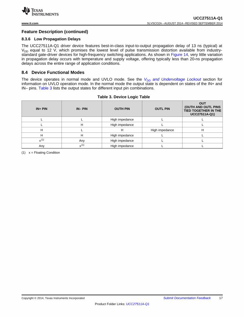
8.4 Device Functional ModesThe device operates in normal mode and UVLO mode. See the VDD and Undervoltage Lockout section forinformation on UVLO operation mode. In the normal mode the output state is dependent on states of the IN+ andIN– pins. Table 3 lists the output states for different input pin combinations.
Table 3. Device Logic TableOUT
(OUTH AND OUTL PINSIN+ PIN IN– PIN OUTH PIN OUTL PIN TIED TOGETHER IN THEUCC27511A-Q1)
L L High impedance L LL H High impedance L LH L H High impedance HH H High impedance L L
x (1) Any High impedance L LAny x (1) High impedance L L
(1) x = Floating Condition
Copyright © 2014, Texas Instruments Incorporated Submit Documentation Feedback 17
Product Folder Links: UCC27511A-Q1
IN+
IN±
GND
VDD
OUTH
OUTL
UCC27511A-Q1
R2
6
5
4
1
2
3
R1Q1 C(OUT)
C
L1
VO
D1
V(LINE)
Rectified AC input
4.5 to 18 V
V(BIAS)
VI
UCC27511A-Q1SLVSCO2A –AUGUST 2014–REVISED SEPTEMBER 2014 www.ti.com
9 Application and Implementation
9.1 Application InformationHigh-current gate-driver devices are required in switching-power applications for a variety of reasons. In order toeffect fast switching of power devices and reduce associated switching power losses, a powerful gate driveremploys between the PWM output of controllers and the gates of the power-semiconductor devices. Further,gate drivers are indispensable when having the PWM controller directly drive the gates of the switching devicesis impossible. With the advent of digital power, this situation will be encountered often encountered because thePWM signal from the digital controller is often a 3.3-V logic signal which is not capable of effectively turning on apower switch.
A level-shifting circuitry is needed to boost the 3.3-V signal to the gate-drive voltage (such as 12 V) in order tofully turn on the power device and minimize conduction losses. Traditional buffer drive circuits based on NPN andPNP bipolar transistors in totem-pole arrangement, being emitter follower configurations, prove inadequate withdigital power because these circuits lack level-shifting capability. Gate drivers effectively combine both the level-shifting and buffer-drive functions. Gate drivers also satisfy other needs such as minimizing the effect of high-frequency switching noise by locating the high-current driver physically close to the power switch, driving gate-drive transformers and controlling floating power-device gates, reducing power dissipation and thermal stress incontrollers by moving gate charge power losses into the controller.
Finally, emerging wide bandgap power device technologies, such as GaN based switches, which are capable ofsupporting very high switching frequency operation, are driving very special requirements in terms of gate drivecapability. These requirements include operation at low VDD voltages (5 V or lower), low propagation delays andavailability in compact, low-inductance packages with good thermal capability. In summary gate-driver devicesare extremely important components in switching power combining benefits of high-performance low-costcomponent count and board-space reduction and simplified system design.
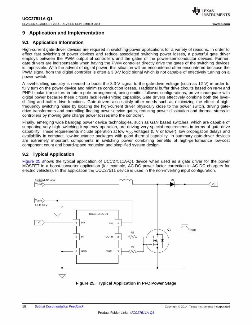
9.2 Typical ApplicationFigure 25 shows the typical application of UCC27511A-Q1 device when used as a gate driver for the powerMOSFET in a boost-converter application (for example, AC-DC power factor correction in AC-DC chargers forelectric vehicles). In this application the UCC27511 device is used in the non-inverting input configuration.
Figure 25. Typical Application in PFC Power Stage
18 Submit Documentation Feedback Copyright © 2014, Texas Instruments Incorporated
Product Folder Links: UCC27511A-Q1

UCC27511A-Q1www.ti.com SLVSCO2A –AUGUST 2014–REVISED SEPTEMBER 2014
Typical Application (continued)9.2.1 Design RequirementsWhen selecting the proper gate driver device for an end application, some design considerations must beevaluated first in order to make the most appropriate selection. Among these considerations are input-to-outputconfiguration, the input threshold type, bias supply voltage levels, peak source and sink currents, availability ofindependent enable and disable functions, propagation delay, power dissipation, and package type.
9.2.2 Detailed Design Procedure
9.2.2.1 Input-to-Output LogicThe design should specify which type of input-to-output configuration should be used. If turning on the powerMOSFET or IGBT when the input signal is in high state is preferred, then the non-inverting configuration must beselected. If turning off the power MOSFET or IGBT when the input signal is in high state is preferred, theinverting configuration must be chosen. The UCC27511A-Q1 device can be configured in either an inverting ornon-inverting input-to-output configuration using the IN– or IN+ pins respectively. To configure the device for usein inverting mode, tie the IN+ pin to VDD and apply the input signal to the IN– pin. For the non-invertingconfiguration, tie the IN– pin to GND and apply the input signal to the IN+ pin.
9.2.2.2 Input Threshold typeThe type of Input voltage threshold determines the type of controller that can be used with the gate driver device.The UCC27511A-Q1 device features a TTL and CMOS-compatible input threshold logic, with wide hysteresis.The threshold voltage levels are low voltage and independent of the VDD supply voltage, which allowscompatibility with both logic-level input signals from microcontrollers as well as higher-voltage input signals fromanalog controllers. See the Electrical Characteristics table for the actual input threshold voltage levels andhysteresis specifications for the UCC27511A-Q1 device.
9.2.2.3 VDD Bias Supply VoltageThe bias supply voltage to be applied to the VDD pin of the device should never exceed the values listed in theRecommended Operating Conditions table. However, different power switches demand different voltage levels tobe applied at the gate terminals for effective turnon and turnoff. With certain power switches, a positive gatevoltage may be required for turnon and a negative gate voltage may be required for turnoff, in which case theVDD bias supply equals the voltage differential. With a wide operating range from 4.5 V to 18 V, the UCC27511A-Q1 device can be used to drive a variety of power switches, such as Si MOSFETs (for example, VGS = 4.5 V, 10V, 12 V), IGBTs (VGE = 15 V, 18 V), and wide-bandgap power semiconductors (such as GaN, certain types ofwhich allow no higher than 6 V to be applied to the gate terminals).
9.2.2.4 Peak Source and Sink CurrentsGenerally, switching the speed of the power switch during turnon and turnoff should be as fast as possible inorder to minimize switching power losses. The gate driver device must be able to provide the required peakcurrent for achieving the targeted switching speeds for the targeted power MOSFET.
Using the example of a power MOSFET, the system requirement for the switching speed is typically described interms of the slew rate of the drain-to-source voltage of the power MOSFET (such as dVDS/dt). For example, thesystem requirement might state that a SPP20N60C3 power MOSFET must be turned-on with a dVDS/dt of 20V/ns or higher under a DC bus voltage of 400 V in a continuous-conduction-mode (CCM) boost PFC-converterapplication. This type of application is an inductive hard-switching application and reducing switching powerlosses is critical. This requirement means that the entire drain-to-source voltage swing during power MOSFETturn-on event (from 400 V in the OFF state to VDS(on) in on state) must be completed in approximately 20 ns orless. When the drain-to-source voltage swing occurs, the Miller charge of the power MOSFET (QGD parameter inSPP20N60C3 power MOSFET data sheet = 33 nC typical) is supplied by the peak current of gate driver.According to power MOSFET inductive switching mechanism, the gate-to-source voltage of the power MOSFETat this time is the Miller plateau voltage, which is typically a few volts higher than the threshold voltage of thepower MOSFET, VGS(TH).
Copyright © 2014, Texas Instruments Incorporated Submit Documentation Feedback 19
Product Folder Links: UCC27511A-Q1

UCC27511A-Q1SLVSCO2A –AUGUST 2014–REVISED SEPTEMBER 2014 www.ti.com
Typical Application (continued)In order to achieve the targeted dVDS/dt, the gate driver must be capable of providing the QGD charge in 20 ns orless. In other words a peak current of 1.65 A (= 33 nC / 20 ns) or higher must be provided by the gate driver. TheUCC27511-Q1 gate driver is capable of providing 4-A peak sourcing current which clearly exceeds the designrequirement and has the capability to meet the switching speed needed. The 2.4x overdrive capability providesan extra margin against part-to-part variations in the QGD parameter of the power MOSFET along with additionalflexibility to insert external gate resistors and fine tune the switching speed for efficiency versus EMIoptimizations.
However, in practical designs the parasitic trace inductance in the gate drive circuit of the PCB will have adefinitive role to play on the power MOSFET switching speed. The effect of this trace inductance is to limit thedI/dt of the output current pulse of the gate driver. In order to illustrate this, consider output current pulsewaveform from the gate driver to be approximated to a triangular profile, where the area under the triangle (½ ×IPEAK × time) would equal the total gate charge of the power MOSFET (QG parameter in SPP20N60C3 powerMOSFET datasheet = 87 nC typical). If the parasitic trace inductance limits the dI/dt then a situation may occur inwhich the full peak current capability of the gate driver is not fully achieved in the time required to deliver the QGrequired for the power MOSFET switching. In other words the time parameter in the equation would dominateand the IPEAK value of the current pulse would be much less than the true peak current capability of the device,while the required QG is still delivered. Because of this, the desired switching speed may not be realized, evenwhen theoretical calculations indicate the gate driver is capable of achieving the targeted switching speed. Thus,placing the gate driver device very close to the power MOSFET and designing a tight gate drive-loop withminimal PCB trace inductance is important to realize the full peak-current capability of the gate driver.
9.2.2.5 Enable and Disable FunctionCertain applications demand independent control of the output state of the driver without involving the inputsignal. A pin which offers an enable and disable function achieves this requirement. The UCC27511A-Q1 deviceoffers 2 input pins, IN+ and IN–, both of which control the state of the output as listed in Table 3. Based onwhether an inverting or non-inverting input signal is provided to the driver, the appropriate input pin can beselected as the primary input for controlling the gate driver. The other unused input pin can be conveniently usedfor the enable and disable functionality. If the design does not require an enable function, the unused input pincan be tied to either the VDD pin (in case IN+ is the unused pin), or GND (in case IN– is unused pin) in order toensure it does not affect the output status.
9.2.2.6 Propagation delayThe acceptable propagation delay from the gate driver is dependent on the switching frequency at which it isused and the acceptable level of pulse distortion to the system. The UCC27511A-Q1 device features industrybest-in-class 13-ns (typical) propagation delays which ensures very little pulse distortion and allows operation atvery high-frequencies. See the Switching Characteristics table for the propagation and switching characteristicsof the UCC27511A-Q1 device.
9.2.2.7 Thermal InformationThe useful range of a driver is greatly affected by the drive-power requirements of the load and the thermalcharacteristics of the package. In order for a gate driver to be useful over a particular temperature range thepackage must allow for the efficient removal of the heat produced while keeping the junction temperature withinrated limits. The thermal metrics for the driver package is listed in the Thermal Information table. For detailedinformation regarding the Thermal Information table, please refer to the Application Note from Texas Instrumentsentitled IC Package Thermal Metrics (SPRA953).
The UCC27511A-Q1 device is offered in a SOT-23, 6-pin package (DBV). The Thermal Information section liststhe thermal performance metrics related to SOT-23 package. The ψJT and ψJB metrics are used when estimatingthe die temperature during actual application measurements.
Heat removal occurs primarily through the leads of the device and the PCB traces connected to the leads.
20 Submit Documentation Feedback Copyright © 2014, Texas Instruments Incorporated
Product Folder Links: UCC27511A-Q1

2tot (LOAD) DD S G DD SP C V ƒ Q V ƒ= ´ ´ = ´ ´
G (LOAD) DDQ C V= ´
2tot (LOAD) DD SP C V ƒ= ´ ´
2G (LOAD) DD
1E C V
2= ´
P(DC) Q DDP I V= ´
D D(DC) D(SW)P P P= +
UCC27511A-Q1www.ti.com SLVSCO2A –AUGUST 2014–REVISED SEPTEMBER 2014
Typical Application (continued)9.2.2.8 Power DissipationPower dissipation of the gate driver has two portions as shown in Equation 1.
where• PD is the power dissipation• PD(DC) is the DC portion of the power dissipation• PD(SW) is the power dissipated in the gate-driver package during switching (1)
Use Equation 2 to calculate the DC portion of the power dissipation.
where• IQ is the quiescent current for the driver (2)
The quiescent current is the current consumed by the device to bias all internal circuits such as input stage,reference voltage, logic circuits, protections, and also any current associated with switching of internal deviceswhen the driver output changes state (such as charging and discharging of parasitic capacitances, parasiticshoot-through, and others). The UCC27511A-Q1 device features very low quiescent currents (less than 1 mA,see Figure 7) and contains internal logic to eliminate any shoot-through in the output driver stage. Thus the effectof the PD(DC) on the total power dissipation within the gate driver can be assumed to be negligible.
The power dissipated in the gate-driver package during switching (PD(SW)) depends on the following factors:• The gate charge required of the power device (usually a function of the drive voltage VG, which is very close
to input bias supply voltage VDD because of low VO(H) drop-out).• The switching frequency (ƒS)• Use of external gate resistors (R(GATE))
When a driver device is tested with a discrete, capacitive load calculating the power that is required from the biassupply is fairly simple. The energy to charge the capacitor is given by Equation 3.
Where• C(LOAD) is load capacitor• VDD is bias voltage feeding the driver• EG is the energy stored in the capacitor when it is charged to VDD (3)
An equal amount of energy dissipates when the capacitor is charged which leads to a total power loss given byEquation 4.
where• Ptot is the total power loss• ƒS is the switching frequency (4)
The switching load presented by a power MOSFET or IGBT is converted to an equivalent capacitance byexamining the gate charge required to switch the device. This gate charge includes the effects of the inputcapacitance plus the added charge needed to swing the drain voltage of the power device as it switches betweenthe ON and OFF states. Most manufacturers provide specifications of typical and maximum gate charge, in nC,to switch the device under specified conditions. Using the gate charge, QG, determine the power that must bedissipated when charging a capacitor (calculated using Equation 5, to provide Equation 6).
(5)
(6)
Copyright © 2014, Texas Instruments Incorporated Submit Documentation Feedback 21
Product Folder Links: UCC27511A-Q1

(OFF) (ON)D(SW) G DD S
(OFF) (GATE) (ON) (GATE)
R RP 0.5 Q V ƒ
R R R R
æ ö= ´ ´ ´ ´ +ç ÷
ç ÷+ +è ø
UCC27511A-Q1SLVSCO2A –AUGUST 2014–REVISED SEPTEMBER 2014 www.ti.com
Typical Application (continued)This power, Ptot, is dissipated in the resistive elements of the circuit when the MOSFET or IGBT is being turnedon or off. Half of the total power is dissipated when the load capacitor is charged during turnon, and the otherhalf is dissipated when the load capacitor is discharged during turnoff. When no external gate resistor isemployed between the driver and MOSFET or IGBT, this power is completely dissipated inside the driverpackage. With the use of external gate-drive resistors, the power dissipation is shared between the internalresistance of driver and external gate resistor in accordance to the ratio of the resistance (more power dissipatedin the higher resistance component). Based on this simplified analysis, the driver power dissipation duringswitching is calculated in Equation 7.
where• R(OFF) = RO(L)
• R(ON) (effective resistance of pullup structure) = 2.7 × RO(L) (7)
9.2.3 Application CurvesFigure 26 and Figure 27 show the typical switching characteristics of the UCC27511A-Q1 device.
VDD = 10 V C(LOAD) = 1 nF VDD = 10 V C(LOAD) = 1 nF
Figure 26. Typical Turnon Waveform Figure 27. Typical Turnoff Waveform
10 Power Supply RecommendationsThe bias supply voltage range for which the UCC27511A-Q1 device is rated to operate is from 4.5 V to 18 V.The lower end of this range is governed by the internal undervoltage-lockout (UVLO) protection feature on theVDD pin supply circuit blocks. Whenever the driver is in UVLO condition when the VDD pin voltage is below theV(ON) supply start threshold, this feature holds the output low, regardless of the status of the inputs. The upperend of this range is driven by the 20-V absolute maximum voltage rating of the VDD pin of the device (which is astress rating). Keeping a 2-V margin to allow for transient voltage spikes, the maximum recommended voltage forthe VDD pin is 18 V.
The UVLO protection feature also involves a hysteresis function. This means that when the VDD pin bias voltagehas exceeded the threshold voltage and device begins to operate, and if the voltage drops, then the devicecontinues to deliver normal functionality unless the voltage drop exceeds the hysteresis specification VDD(hys).Therefore, ensuring that, while operating at or near the 4.5V range, the voltage ripple on the auxiliary powersupply output is smaller than the hysteresis specification of the device is important to avoid triggering deviceshutdown.
22 Submit Documentation Feedback Copyright © 2014, Texas Instruments Incorporated
Product Folder Links: UCC27511A-Q1

UCC27511A-Q1www.ti.com SLVSCO2A –AUGUST 2014–REVISED SEPTEMBER 2014
During system shutdown, the device operation continues until the VDD pin voltage has dropped below the V(OFF)threshold which must be accounted for while evaluating system shutdown timing design requirements. Likewise,at system startup, the device does not begin operation until the VDD pin voltage has exceeded above the V(ON)threshold.
The quiescent current consumed by the internal circuit blocks of the device is supplied through the VDD pin.Although this fact is well known, recognizing that the charge for source current pulses delivered by the OUTH pinis also supplied through the same VDD pin is important. As a result, every time a current is sourced out of theoutput pins (OUTH), a corresponding current pulse is delivered into the device through the VDD pin. Thusensuring that local bypass capacitors are provided between the VDD and GND pins and located as close to thedevice as possible for the purpose of decoupling is important. A low ESR, ceramic surface mount capacitor is amust. TI recommends to have 2 capacitors; a 100-nF ceramic surface-mount capacitor which can be nudgedvery close to the pins of the device and another surface-mount capacitor of few microfarads added in parallel.
11 Layout
11.1 Layout GuidelinesProper PCB layout is extremely important in a high-current fast-switching circuit to provide appropriate deviceoperation and design robustness. The UCC27511A-Q1 gate driver incorporates short-propagation delays andpowerful output stages capable of delivering large current peaks with very fast rise and fall times at the gate ofpower switch to facilitate voltage transitions very quickly. At higher VDD voltages, the peak-current capability iseven higher (4-A/8-A peak current is at VDD equal to 12 V). Very high di/dt causes unacceptable ringing if thetrace lengths and impedances are not well controlled. The following circuit-layout guidelines are stronglyrecommended when designing with these high-speed drivers.• Place the driver device as close as possible to power device in order to minimize the length of high-current
traces between the output pins and the gate of the power device.• Place the VDD-bypass capacitors between the VDD pin and GND as close as possible to the driver with
minimal trace length to improve the noise filtering. These capacitors support high-peak current being drawnfrom VDD during turnon of power MOSFET. The use of low inductance surface-mount components such aschip resistors and chip capacitors is highly recommended.
• The turnon and turnoff current-loop paths (driver device, power MOSFET, and VDD bypass capacitor) shouldbe minimized as much as possible in order to keep the stray inductance to a minimum. High dI/dt isestablished in these loops at two instances – during turnon and turnoff transients, which will induce significantvoltage transients on the output pin of the driver device and gate of the power switch.
• Wherever possible, parallel the source and return traces, taking advantage of flux cancellation.• Separate power traces and signal traces, such as the output and input signals.• Minimize noise coupling from one current loop to another with star-point grounding or other techniques. The
GND of the driver should be connected to the other circuit nodes such as source of power switch, ground ofPWM controller, and others at one single point. The connected paths should be as short as possible toreduce inductance and be as wide as possible to reduce resistance.
• Use a ground plane to provide noise shielding. Fast rise and fall times at OUT may corrupt the input signalsduring transition. The ground plane must not be a conduction path for any current loop. Instead the groundplane must be connected to the star-point with one single trace to establish the ground potential. In additionto noise shielding, the ground plane can help in power dissipation as well.
• In noisy environments, tying the unused Input pin of UCC27511A-Q1 device to the VDD (in case of IN+) pin orGND (in case of IN–) using short traces in order to ensure that the output is enabled and to prevent noisefrom causing malfunction in the output may be necessary.
Copyright © 2014, Texas Instruments Incorporated Submit Documentation Feedback 23
Product Folder Links: UCC27511A-Q1
UCC27511A-Q1SLVSCO2A –AUGUST 2014–REVISED SEPTEMBER 2014 www.ti.com
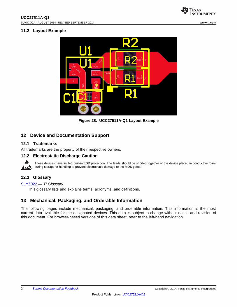
11.2 Layout Example
Figure 28. UCC27511A-Q1 Layout Example
12 Device and Documentation Support
12.1 TrademarksAll trademarks are the property of their respective owners.
12.2 Electrostatic Discharge CautionThese devices have limited built-in ESD protection. The leads should be shorted together or the device placed in conductive foamduring storage or handling to prevent electrostatic damage to the MOS gates.
12.3 GlossarySLYZ022 — TI Glossary.
This glossary lists and explains terms, acronyms, and definitions.
13 Mechanical, Packaging, and Orderable InformationThe following pages include mechanical, packaging, and orderable information. This information is the mostcurrent data available for the designated devices. This data is subject to change without notice and revision ofthis document. For browser-based versions of this data sheet, refer to the left-hand navigation.
24 Submit Documentation Feedback Copyright © 2014, Texas Instruments Incorporated
Product Folder Links: UCC27511A-Q1

PACKAGE OPTION ADDENDUM
www.ti.com 29-Aug-2014
Addendum-Page 1
PACKAGING INFORMATION
Orderable Device Status(1)
Package Type PackageDrawing
Pins PackageQty
Eco Plan(2)
Lead/Ball Finish(6)
MSL Peak Temp(3)
Op Temp (°C) Device Marking(4/5)
Samples
UCC27511AQDBVRQ1 ACTIVE SOT-23 DBV 6 3000 Green (RoHS& no Sb/Br)
CU NIPDAU Level-2-260C-1 YEAR -40 to 125 EAKQ
(1) The marketing status values are defined as follows:ACTIVE: Product device recommended for new designs.LIFEBUY: TI has announced that the device will be discontinued, and a lifetime-buy period is in effect.NRND: Not recommended for new designs. Device is in production to support existing customers, but TI does not recommend using this part in a new design.PREVIEW: Device has been announced but is not in production. Samples may or may not be available.OBSOLETE: TI has discontinued the production of the device.
(2) Eco Plan - The planned eco-friendly classification: Pb-Free (RoHS), Pb-Free (RoHS Exempt), or Green (RoHS & no Sb/Br) - please check http://www.ti.com/productcontent for the latest availabilityinformation and additional product content details.TBD: The Pb-Free/Green conversion plan has not been defined.Pb-Free (RoHS): TI's terms "Lead-Free" or "Pb-Free" mean semiconductor products that are compatible with the current RoHS requirements for all 6 substances, including the requirement thatlead not exceed 0.1% by weight in homogeneous materials. Where designed to be soldered at high temperatures, TI Pb-Free products are suitable for use in specified lead-free processes.Pb-Free (RoHS Exempt): This component has a RoHS exemption for either 1) lead-based flip-chip solder bumps used between the die and package, or 2) lead-based die adhesive used betweenthe die and leadframe. The component is otherwise considered Pb-Free (RoHS compatible) as defined above.Green (RoHS & no Sb/Br): TI defines "Green" to mean Pb-Free (RoHS compatible), and free of Bromine (Br) and Antimony (Sb) based flame retardants (Br or Sb do not exceed 0.1% by weightin homogeneous material)
(3) MSL, Peak Temp. - The Moisture Sensitivity Level rating according to the JEDEC industry standard classifications, and peak solder temperature.
(4) There may be additional marking, which relates to the logo, the lot trace code information, or the environmental category on the device.
(5) Multiple Device Markings will be inside parentheses. Only one Device Marking contained in parentheses and separated by a "~" will appear on a device. If a line is indented then it is a continuationof the previous line and the two combined represent the entire Device Marking for that device.
(6) Lead/Ball Finish - Orderable Devices may have multiple material finish options. Finish options are separated by a vertical ruled line. Lead/Ball Finish values may wrap to two lines if the finishvalue exceeds the maximum column width.
Important Information and Disclaimer:The information provided on this page represents TI's knowledge and belief as of the date that it is provided. TI bases its knowledge and belief on informationprovided by third parties, and makes no representation or warranty as to the accuracy of such information. Efforts are underway to better integrate information from third parties. TI has taken andcontinues to take reasonable steps to provide representative and accurate information but may not have conducted destructive testing or chemical analysis on incoming materials and chemicals.TI and TI suppliers consider certain information to be proprietary, and thus CAS numbers and other limited information may not be available for release.
In no event shall TI's liability arising out of such information exceed the total purchase price of the TI part(s) at issue in this document sold by TI to Customer on an annual basis.

PACKAGE OPTION ADDENDUM
www.ti.com 29-Aug-2014
Addendum-Page 2

TAPE AND REEL INFORMATION
*All dimensions are nominal
Device PackageType
PackageDrawing
Pins SPQ ReelDiameter
(mm)
ReelWidth
W1 (mm)
A0(mm)
B0(mm)
K0(mm)
P1(mm)
W(mm)
Pin1Quadrant
UCC27511AQDBVRQ1 SOT-23 DBV 6 3000 178.0 9.0 3.23 3.17 1.37 4.0 8.0 Q3
PACKAGE MATERIALS INFORMATION
www.ti.com 30-Aug-2014
Pack Materials-Page 1

*All dimensions are nominal
Device Package Type Package Drawing Pins SPQ Length (mm) Width (mm) Height (mm)
UCC27511AQDBVRQ1 SOT-23 DBV 6 3000 180.0 180.0 18.0
PACKAGE MATERIALS INFORMATION
www.ti.com 30-Aug-2014
Pack Materials-Page 2


IMPORTANT NOTICE
Texas Instruments Incorporated and its subsidiaries (TI) reserve the right to make corrections, enhancements, improvements and otherchanges to its semiconductor products and services per JESD46, latest issue, and to discontinue any product or service per JESD48, latestissue. Buyers should obtain the latest relevant information before placing orders and should verify that such information is current andcomplete. All semiconductor products (also referred to herein as “components”) are sold subject to TI’s terms and conditions of salesupplied at the time of order acknowledgment.TI warrants performance of its components to the specifications applicable at the time of sale, in accordance with the warranty in TI’s termsand conditions of sale of semiconductor products. Testing and other quality control techniques are used to the extent TI deems necessaryto support this warranty. Except where mandated by applicable law, testing of all parameters of each component is not necessarilyperformed.TI assumes no liability for applications assistance or the design of Buyers’ products. Buyers are responsible for their products andapplications using TI components. To minimize the risks associated with Buyers’ products and applications, Buyers should provideadequate design and operating safeguards.TI does not warrant or represent that any license, either express or implied, is granted under any patent right, copyright, mask work right, orother intellectual property right relating to any combination, machine, or process in which TI components or services are used. Informationpublished by TI regarding third-party products or services does not constitute a license to use such products or services or a warranty orendorsement thereof. Use of such information may require a license from a third party under the patents or other intellectual property of thethird party, or a license from TI under the patents or other intellectual property of TI.Reproduction of significant portions of TI information in TI data books or data sheets is permissible only if reproduction is without alterationand is accompanied by all associated warranties, conditions, limitations, and notices. TI is not responsible or liable for such altereddocumentation. Information of third parties may be subject to additional restrictions.Resale of TI components or services with statements different from or beyond the parameters stated by TI for that component or servicevoids all express and any implied warranties for the associated TI component or service and is an unfair and deceptive business practice.TI is not responsible or liable for any such statements.Buyer acknowledges and agrees that it is solely responsible for compliance with all legal, regulatory and safety-related requirementsconcerning its products, and any use of TI components in its applications, notwithstanding any applications-related information or supportthat may be provided by TI. Buyer represents and agrees that it has all the necessary expertise to create and implement safeguards whichanticipate dangerous consequences of failures, monitor failures and their consequences, lessen the likelihood of failures that might causeharm and take appropriate remedial actions. Buyer will fully indemnify TI and its representatives against any damages arising out of the useof any TI components in safety-critical applications.In some cases, TI components may be promoted specifically to facilitate safety-related applications. With such components, TI’s goal is tohelp enable customers to design and create their own end-product solutions that meet applicable functional safety standards andrequirements. Nonetheless, such components are subject to these terms.No TI components are authorized for use in FDA Class III (or similar life-critical medical equipment) unless authorized officers of the partieshave executed a special agreement specifically governing such use.Only those TI components which TI has specifically designated as military grade or “enhanced plastic” are designed and intended for use inmilitary/aerospace applications or environments. Buyer acknowledges and agrees that any military or aerospace use of TI componentswhich have not been so designated is solely at the Buyer's risk, and that Buyer is solely responsible for compliance with all legal andregulatory requirements in connection with such use.TI has specifically designated certain components as meeting ISO/TS16949 requirements, mainly for automotive use. In any case of use ofnon-designated products, TI will not be responsible for any failure to meet ISO/TS16949.
Products ApplicationsAudio www.ti.com/audio Automotive and Transportation www.ti.com/automotiveAmplifiers amplifier.ti.com Communications and Telecom www.ti.com/communicationsData Converters dataconverter.ti.com Computers and Peripherals www.ti.com/computersDLP® Products www.dlp.com Consumer Electronics www.ti.com/consumer-appsDSP dsp.ti.com Energy and Lighting www.ti.com/energyClocks and Timers www.ti.com/clocks Industrial www.ti.com/industrialInterface interface.ti.com Medical www.ti.com/medicalLogic logic.ti.com Security www.ti.com/securityPower Mgmt power.ti.com Space, Avionics and Defense www.ti.com/space-avionics-defenseMicrocontrollers microcontroller.ti.com Video and Imaging www.ti.com/videoRFID www.ti-rfid.comOMAP Applications Processors www.ti.com/omap TI E2E Community e2e.ti.comWireless Connectivity www.ti.com/wirelessconnectivity
Mailing Address: Texas Instruments, Post Office Box 655303, Dallas, Texas 75265Copyright © 2015, Texas Instruments Incorporated