vmivme-4100 16-channel 12-bit digital-to-analog converter board
TRANSCRIPT

VMIVME-4100
16-CHANNEL 12-BIT DIGITAL-TO-ANALOGCONVERTER BOARD
INSTRUCTION MANUAL
DOCUMENT NO. 500-004100-000
Revised April 21, 1992
VME MICROSYSTEMS INTERNATIONAL CORPORATION12090 SOUTH MEMORIAL PARKWAY
HUNTSVILLE, AL 35803-3308(205) 880-0444 FAX: (205) 882-0859
1-800-322-3616

NOTICE
The information in this document has been carefully checked and isbelieved to be entirely reliable. While all reasonable efforts to ensure accuracyhave been taken in the preparation of this manual, VMIC assumes no responsibilityresulting from omissions or errors in this manual, or from the use of informationcontained herein.
VMIC reserves the right to make any changes, without notice, to this orany of VMIC’s products to improve reliability, performance, function, or design.
VMIC does not assume any liability arising out of the application or useof any product or circuit described herein; nor does VMIC convey any licenseunder its patent rights or the rights of others.
VME Microsystems International Corporation
All Rights Reserved
This document shall not be duplicated, nor its contents used for anypurpose, unless granted express written permission from VMIC.
Copyright © January 1986 byVME Microsystems International Corporation

RECORD OF REVISIONS
REVISION LETTER
DATE PAGES INVOLVED CHANGE NUMBER
VME MICROSYSTEMS INT’L CORP. PAGE NO.REV LTR
VMIC
12090 South Memorial Parkway • Huntsville, Al 35803 • (205) 880-0444 iiDOC. NO. 500-004100-000
A 03/06/86 Entire Manual Manual - 01
B 11/06/86 Schematic 4100 - 05
R
C 03/25/87 P. 2-3, P. 4-1, Cover, and Record of Revisions Page
4100 - 07
D 09/30/88 Update Appendix A 88-0091
E 10/19/88 Update Appendix A 88-0194
F 11/06/88 Revise Manual 88-0319
G 05/03/89 Cover, pages ii, vi, vii, 3-2, 3-6, 3-10, 3-11, 5-5, 5-8, 5-10, Section 6, and Appendix A. Reformat Manual.
89-0017
H 08/14/89 Cover, page ii, Appendix A 89-0083
J 10/12/90 Cover, pages ii, and Appendix A 89-0195
L 03/12/91 Cover, page ii, Appendix A 91-0029
M 05/28/91 Cover, page ii, vii, Section 2, page 3-2, Section 5 and 6, and Appendix A
91-0148
K 10/12/90 Cover, pages ii, 4-4, and Appendix A 90-0137
N 12/19/91 Cover, pages ii, 2-7, and Appendix A 91-0320
P 01/24/92 Cover, page ii, and Appendix A 92-0015
R 04/21/92 Cover, page ii, Sections 2 and 6, and Appendix A
92-0110

iii
VMICSAFETY SUMMARY
THE FOLLOWING GENERAL SAFETY PRECAUTIONS MUST BE OBSERVED DURINGALL PHASES OF THE OPERATION, SERVICE, AND REPAIR OF THIS PRODUCT.FAILURE TO COMPLY WITH THESE PRECAUTIONS OR WITH SPECIFIC WARNINGSELSEWHERE IN THIS MANUAL VIOLATES SAFETY STANDARDS OF DESIGN,MANUFACTURE, AND INTENDED USE OF THIS PRODUCT. VME MICROSYSTEMSINTERNATIONAL CORPORATION ASSUMES NO LIABILITY FOR THE CUSTOMER’SFAILURE TO COMPLY WITH THESE REQUIREMENTS.
GROUND THE SYSTEM To minimize shock hazard, the chassis and system cabinet must be connected to anelectrical ground. A three-conductor AC power cable should be used. The powercable must either be plugged into an approved three-contact electrical outlet or usedwith a three-contact to two-contact adapter with the grounding wire (green) firmlyconnected to an electrical ground (safety ground) at the power outlet.
DO NOT OPERATE IN AN EXPLOSIVE ATMOSPHERE Do not operate the system in the presence of flammable gases or fumes. Operation ofany electrical system in such an environment constitutes a definite safety hazard.
KEEP AWAY FROM LIVE CIRCUITS Operating personnel must not remove product covers. Component replacement andinternal adjustments must be made by qualified maintenance personnel. Do notreplace components with power cable connected. Under certain conditions,dangerous voltages may exist even with the power cable removed. To avoid injuries,always disconnect power and discharge circuits before touching them.
DO NOT SERVICE OR ADJUST ALONE Do not attempt internal service or adjustment unless another person, capable ofrendering first aid and resuscitation, is present.
DO NOT SUBSTITUTE PARTS OR MODIFY SYSTEM Because of the danger of introducing additional hazards, do not install substitute partsor perform any unauthorized modification to the product. Return the product to VMEMicrosystems International Corporation for service and repair to ensure that safetyfeatures are maintained.
DANGEROUS PROCEDURE WARNINGS Warnings, such as the example below, precede only potentially dangerousprocedures throughout this manual. Instructions contained in the warnings must befollowed.
WARNING DANGEROUS VOLTAGES, CAPABLE OF CAUSING DEATH, ARE PRESENT IN THISSYSTEM. USE EXTREME CAUTION WHEN HANDLING, TESTING, AND ADJUSTING.

!
OR
OR
WARNING
***************
***************
***
***
CAUTION
SAFETY SYMBOLSGENERAL DEFINITIONS OF SAFETY SYMBOLS USED IN THIS MANUAL
NOTE:
iv
Instruction manual symbol: the product is marked with this symbol when it is necessary for the user to refer to the instruction manual in order to protect against damage to the system.
Indicates dangerous voltage (terminals fed from the interior by voltage exceeding 1000 volts are so marked).
Protective conductor terminal. For protection against electrical shock in case of a fault. Used with field wiring terminals to indicate the terminal which must be connected to ground before operating equipment.
Low-noise or noiseless, clean ground (earth) terminal. Used for a signal common, as well as providing protection against electrical shock in case of a fault. Before operating the equipment, terminal marked with this symbol must be connected to ground in the manner described in the installation (operation) manual.
Frame or chassis terminal. A connection to the frame (chassis) of the equipment which normally includes all exposed metal structures.
Alternating current (power line).
Direct current (power line).
Alternating or direct current (power line).
The WARNING sign denotes a hazard. It calls attention to a procedure, a practice, a condition, or the like, which, if not correctly performed or adhered to, could result in injury or death to personnel.
The CAUTION sign denotes a hazard. It calls attention to an operating a procedure, a practice, a condition, or the like, which, if not correctly performed or adhered to, could result in damage to or destruction of part or all of the system.
The NOTE sign denotes important information. It calls attention to a procedure, a practice, a condition, or the like, which is essential to highlight.

500-004100-000
v
VMIVME-410016-CHANNEL 12-BIT DIGITAL-TO-ANALOG
CONVERTER BOARD
TABLE OF CONTENTS
Page SECTION 1. VMIVME-4100 16-CHANNEL 12-BIT DIGITAL-TO-
ANALOG CONVERTER BOARD
1.1 INTRODUCTION......................................................................................1-11.2 VMIVME-4100 12-BIT DAC BOARD BRIEF OVERVIEW.........................1-11.3 REFERENCE MATERIAL .......................................................................1-3
SECTION 2. PHYSICAL DESCRIPTION AND SPECIFICATIONS
SECTION 3. THEORY OF OPERATION
3.1 INTRODUCTION......................................................................................3-13.2 IMMEDIATE DAC UPDATE MODE..........................................................3-13.3 DELAYED DAC UPDATE MODE.............................................................3-13.3.1 Program Control Update...........................................................................3-43.3.2 External Trigger Update ...........................................................................3-43.4 VMIVME-4100 TEST MODE DESCRIPTION...........................................3-43.4.1 Using the VMIVME-4100 to Test the Multiplexer Channels of the
VMIVME-3200..........................................................................................3-73.5 VMEbus INTERFACE DESCRIPTION .....................................................3-73.6 P2 CONNECTOR I/O SIGNAL DEFINITION............................................3-10
SECTION 4. PROGRAMMING
4.1 INTRODUCTION......................................................................................4-14.2 DAC BOARD PROGRAMMING OPTIONS ..............................................4-14.2.1 Introduction...............................................................................................4-14.2.2 Immediate DAC Update Mode..................................................................4-14.3 DELAYED DAC UPDATE MODE.............................................................4-34.4 TEST MODE PROGRAMMING................................................................4-34.5 MC68000 ASSEMBLY LANGUAGE PROGRAMMING OF THE
VMIVME-4100 DAC BOARD....................................................................4-74.6 PROGRAM EXAMPLE (DELAYED DAC UPDATE MODE) .....................4-7

500-004100-000
vi
TABLE OF CONTENTS (Continued)
Page
SECTION 5. CONFIGURATION AND INSTALLATION
5.1 UNPACKING PROCEDURES..................................................................5-15.2 PHYSICAL INSTALLATION .....................................................................5-15.3 INSTALLATION........................................................................................5-15.4 BEFORE APPLYING POWER: CHECKLIST ..........................................5-25.4.1 DAC Board Installation .............................................................................5-35.5 BOARD ADDRESS SELECTION-SWITCHES .........................................5-35.6 ADDRESS MODIFIER RESPONSE SELECTION....................................5-35.7 DAC UPDATE MODE SELECT JUMPERS..............................................5-65.8 EXTERNAL DAC UPDATE TRIGGER ENABLE/DISABLE ......................5-65.9 CALIBRATING THE +10 VOLT PRECISION REFERENCE ....................5-65.10 CONNECTOR DESCRIPTIONS ..............................................................5-75.11 ANALOG OUTPUT ACCURACY WHEN OPTIONAL OUTPUT
ISOLATION HARDWARE IS USED .........................................................5-7
SECTION 6. MAINTENANCE AND WARRANTY
6.1 MAINTENANCE .......................................................................................6-16.2 MAINTENANCE PRINTS .........................................................................6-16.3 WARRANTY.............................................................................................6-16.4 OUT-OF-WARRANTY REPAIR POLICY..................................................6-26.4.1 Repair Category .......................................................................................6-36.4.2 Repair Pricing...........................................................................................6-36.4.3 Payment ...................................................................................................6-36.4.4 Shipping Charges.....................................................................................6-46.4.5 Shipping Instructions ................................................................................6-46.4.6 Warranty on Repairs.................................................................................6-46.4.7 Exclusions ................................................................................................6-4
LIST OF FIGURES
Figure Page
1.1-1 16-Channel DAC Board............................................................................1-23.1-1 VMIVME-4100 Board................................................................................3-23.1-2 Analog Output Isolation Switches .............................................................3-33.4-1 VMIC High Performance Analog Input/Output Configuration ....................3-5

500-004100-000
vii
TABLE OF CONTENTS (Concluded)
LIST OF FIGURES (Concluded)
Figure Page
3.4-2 Analog Output Isolation Switches........................................................ 3-63.4-3 Test Bus Logic..................................................................................... 3-83.5-1 VMEbus Interface Logic and Interface Signals.................................... 3-93.5-2 DAC Board Power ............................................................................... 3-114.1-1 Control Status Register and DAC Channels Address Map.................. 4-24.5-1 DAC Programming Sequence (Immediate DAC Start Convert
Mode) .................................................................................................. 4-84.5-2 Program Example (Immediate DAC Update Mode)............................. 4-94.6-1 DAC Programming Sequence (Delayed DAC Update Mode).............. 4-104.6-2 Program Example (Delayed DAC Update Mode) ................................ 4-115.5-1 Base Address DIP Switch Setup ......................................................... 5-45.5-2 Jumper and Switch Locations on VMIVME-4100 (Component Side
Shown) ................................................................................................ 5-55.7-1 Jumper Configuration .......................................................................... 5-65.10-1 P2 Connector - Pin Assignments......................................................... 5-85.10-2 P3 Connector - Pin Assignments......................................................... 5-9
LIST OF TABLES
Table Page
4.2.2-1 DAC Data Format Analog Output vs Digital Input (±10 V Scale)......... 4-44.2.2-2 Control Register Data Format and Definitions ..................................... 4-54.2.2-3 Programming the CSR for Different Analog Output Variations - Bit
Definitions............................................................................................ 4-64.5-1 Analog Output Control in Immediate Update Mode ............................. 4-94.6-1 Analog Output Control in the Delayed DAC Update Mode .................. 4-115.3-1 VMIVME-4100 Factory Set Jumpers and Address Switch
Configurations ..................................................................................... 5-2
APPENDIX
A Assembly Drawing, Parts List, and Schematic

500-004100-000
1-1
SECTION 1
VMIVME-4100 16 CHANNEL 12-BIT DIGITAL-TO-ANALOGCONVERTER BOARD
1.1 INTRODUCTION
The VMIVME-4100 16-Channel 12-Bit Digital-to-Analog Converter (DAC)Board delivers ±10 V outputs with positive true offset binary input coding. The DACBoard features double buffered data latches, buffered voltage outputs, andselectable external or internal update control strobes. The DAC Board may beordered with Built-in-Test hardware that can isolate the 16 analog outputs from fieldconnections during diagnostic testing. In the test mode analog outputs aremultiplexed to an analog test bus on the VME P2 backplane (user I/O pins) foranalog-to-digital conversion by VMIC's Analog-to-Digital Converter (ADC) Board(VMIVME-3100). A front panel Fail LED is provided for quick fault locationidentification. The DAC Board is shown in Figure 1.1-1.
This document will primarily describe the operation of the DAC Board,but some details of the VMIVME-3100 12-Bit ADC Board and the VMIVME-320032-Channel Multiplexer Board will be included for clarity. It is also intended to givethe user a better understanding of the test capabilities of a data acquisition systemusing the DAC Board in conjunction with the VMIC MUX Expander Board,(VMIVME-3200) and the ADC Board, (VMIVME-3100).
For a thorough understanding the reader should have access to thefollowing documents:
VMIVME-3200 32 Channel Analog Input Instruction Manual, Document No.500-003200-000
VMIVME-3100 12-Bit Analog-to-Digital Converter Board Instruction ManualDocument No. 500-003100-000
VMIC Analog Input/Output Products (with Built-in-Test) Configuration Guide,Document No. 825-000000-005
1.2 VMIVME-4100 12-BIT DAC BOARD BRIEF OVERVIEW
The primary features of the 4100 DAC Board are as follows:
a. Buffered voltage outputb. Double buffered data latches

500-004100-000
1-2

500-004100-000
1-3
c. 16 channels per cardd. 12-bit DACse. Front panel Fail LEDf. High reliability Din type 96-pin I/O connectorsg. Multiplexed programmable outputs for testing analog input
multiplexer cardsh. Multiplexed programmable outputs for testing analog outputsi. Individually keyed VME connector designj. Double Eurocard form factork. All 16 DAC outputs can be updated by one of the following three user
selectable methods: (1) Each DAC can be immediately updated when a 12-bit positive
true offset binary word is written to the DACs address. (2) Any DAC may be loaded with new data and then be converted
some time later by the user under program control. (3) Any DAC that has been previously loaded with new data may be
updated by an external TTL compatible device.l. 5 mA output drive currentm. Single +5 V supply operationn. Factory trimmed gain and offset - requires no calibration
A unique feature of the VMIVME-4100 is the Built-in-Test logic that allowsthe testing of any one of the analog output channels through the use of an on-board multiplexer and the VMIVME-3100 ADC Board. When in test mode, the fieldconnections through connector P3 may be isolated and any of the 16 channelsmay be routed to the 12-bit ADC Board via VMIC’s Analog Backplane (AMXbusTM).An ADC Board under program control may have the analog signal converted to a12-bit digital word and compared with the original 12-bit word written to the DACBoard. In this manner, each of the 16 analog output channels may be verifiedwithout disturbing the field connected devices. The analog output channels mayalso be multiplexed to the Analog Test Bus, simultaneously controlling the P3connected field devices, providing real-time fault detection of the outputs. If a boardfails its self-test, a Fail LED on the front panel may be turned on to indicate theboard is in a failed condition. The complete operation and requirements for theself-test mode are explained in detail in this manual in Section 3, Theory ofOperation, and Section 4, Programming.
1.3 REFERENCE MATERIAL
The reader should refer to "The VMEbus Specification" for a detailedexplanation of VMEbus. "The VMEbus Specification" is available from thefollowing source:

500-004100-000
1-4
VITAVMEbus International Trade Association
10229 N. Scottsdale RoadScottsdale, AZ 85253
(602) 951-8866
The following Application and Configuration Guides are available fromVMIC to assist the user in the selection, specification, and implementation ofsystems based on VMIC’s products.
TITLE DOCUMENT NO.
Digital Input Board Application Guide 825-000000-000Analog I/O Products (with Built-in-Test) Configuration Guide 825-000000-005Synchro/Resolver (Built-in-Test) Subsystem Configuration Guide 825-000000-004Change of State Application Guide 825-000000-002Connector and I/O Cable Application Guide 825-000000-006Low Level Analog I/O Configuration Guide 825-000000-001Digital I/O (with Built-in-Test) Product Line Description 825-000000-003

500-004100-000
2-1
SECTION 2
PHYSICAL DESCRIPTION AND SPECIFICATIONS
REFER TO 800-004100-000 SPECIFICATION

500-004100-000
3-1
SECTION 3
THEORY OF OPERATION
3.1 INTRODUCTION
The Digital-to-Analog Converter (DAC) Board performs digital-to-analogconversion on 12-bit positive true offset binary input coded words, with an analogoutput range of -10 to +10 volts. This provides for a resolution of 4.88mV for eachdigital input of 1 LSB change. The buffered output voltage settles to within 1/2 LSBin 8 microseconds (max).
The VMIVME-4100 offers high channel density by using four quad 12-bitDigital-to-Analog (DA) Converters. A Control Status Register (CSR) is loaded bythe processor, and this register controls the functioning of the board. The CSR canbe read by the processor at any time. The DAC Board block diagram is shown inFigure 3.1-1, and the four quad DACs are represented in Figure 3.1-2.
Each of the 16 DACs is preceded by double-buffered data latches. Thedata latches allow versatility in the way that DAC analog output may be updated.
There are three methods by which new data can be converted by a DAC.Each method is enabled/disabled by on-board jumpers and is further controlled bya control register that must be loaded by the user. The control register contents aredescribed in Tables 4.2.2-2 and 4.2.2-3, pp. 4-5 and 4-6.
3.2 IMMEDIATE DAC UPDATE MODE
The processor unit sends the 12-bit word to be converted to the firstregister of the selected DAC. If that DAC channel has previously been jumperedto, it will automatically pass the contents of the first DAC register into the secondregister and update the analog output. There are four jumpers, each oneenables/disables four DAC channels to be in the immediate update mode, asdescribed above, or the delayed update mode, as described below. Jumperdefinition and locations are described in Section 5.7.
3.3 DELAYED DAC UPDATE MODE
In the delayed DAC update mode, the processor sends the 12-bit word tobe converted to the first DAC register of the selected DAC. The data is stored thereand transferred to the second DAC register in one of two possible methods, asdescribed in Sections 3.3.1 and 3.3.2.

VM
Ebu
sC
OM
PA
TIB
ILIT
YLO
GIC
AD
DR
ES
SR
EG
IST
ER
CO
NT
RO
LS
TA
TU
SR
EG
IST
ER
QU
AD
12-B
IT D
/AC
ON
VE
RT
ER
S
QU
AD
12-B
IT D
/AC
ON
VE
RT
ER
S
QU
AD
12-B
IT D
/AC
ON
VE
RT
ER
S
QU
AD
12-B
IT D
/AC
ON
VE
RT
ER
S
OP
ER
AT
ION
AN
D C
ON
TR
OL
LOG
IC
V00
V03
V04
V07
V11
V06
V01
2
V01
5
UP
DA
TE
CO
NT
RO
L
TR
AN
SP
AR
EN
TM
OD
E S
ELE
CT
PR
OG
RA
MC
ON
TR
OL
UP
DA
TE
EX
TE
RN
AL
UP
DA
TE
AO
UT
AD
OR
SE
LEC
T
4
16 C
HA
NN
EL
MU
X
V15
V00
DU
AL
SP
DT
SW
ITC
H
AO
TE
ST
SE
LEC
TA
O T
ES
T(S
AO
T)
SE
LEC
TA
IN T
ES
T(S
AIT
)
AO
TE
ST
AIN
TE
ST
AN
ALO
G O
UT
ISO
LAT
ION
SW
ITC
HE
S
TE
ST
MO
DE
(T
M) A
N00
AN
15
V00
V15
M41
00/F
3.1-
1
Fig
ure
3.1-
1. V
MIV
ME
-410
0 B
oard
500-004100-000
3-2

DA
C
SE
LEC
T
(1 O
F 4
)4-
CH
AN
NE
L D
AC
NO
. 1D
AC
RE
G
SE
LEC
T
(1 O
F 2
)
4 24
DA
C
OU
TP
UT
S
1212
INT
ER
NA
L D
AT
A B
US
DA
C S
ELE
CT
(1
OF
4)
4-C
HA
NN
EL
DA
C N
O. 3
DA
C R
EG
SE
LEC
T
(1 O
F 2
)
4
4
2
DA
OU
TP
UT
S
DA
C
SE
LEC
T
(1 O
F 4
)4-
CH
AN
NE
L D
AC
NO
. 2D
AC
RE
G
SE
LEC
T
(1 O
F 2
)
4 24
DA
C
OU
TP
UT
S
1212
DA
C S
ELE
CT
(1
OF
4)
4-C
HA
NN
EL
DA
C N
O. 4
DA
C R
EG
SE
LEC
T
(1 O
F 2
)
4
4
2
DA
OU
TP
UT
S
Fig
ure
3.1-
2. A
nalo
g O
utpu
t Iso
latio
n S
witc
hes
M41
00/F
3.1-
2
500-004100-000
3-3

500-004100-000
3-4
3.3.1 Program Control Update
One way for the transfer to occur is writing a specified control bit to thecontrol register. When the data is transferred to the second register, digital-to-analog conversion begins and the analog output settles to within 1/2 LSB in 8microseconds. Maximum load capacitance is 300 pf. This method of updating theanalog output under program control is useful when more than one DAC channeloutput is desired to change at a precise time. All 16 DAC outputs could besynchronized to change at certain periodic intervals under software control.
3.3.2 External Trigger Update
The second method to update the second storage register, and thereforethe DAC output, is by an external TTL compatible trigger. This trigger must first beenabled to be received by the external trigger circuitry by installing an on-boardjumper, as described in Section 5.8. When the external trigger is received activelow for a minimum of 150ns, then the value stored in the first DAC register will betransferred to the second DAC register to begin conversion. Using this method ofupdate, all conversions can be synchronized to an external device.
3.4 VMIVME-4100 TEST MODE DESCRIPTION
The test mode hardware is optional (refer to VMIC’s Price Guide foroptions) and is only needed when the VMIVME-4100 is used along with theVMIVME-3100 12-bit ADC Board as a minimum and possibly the VMIVME-3200Multiplexer Board. Both of these boards support the Built-in-Test capabilities of the DACBoard and will be further explained here. A typical data acquisitionconfiguration with Built-in-Test capabilities is shown in Figure 3.4-1. Up to 16multiplexer boards or 16 DAC Boards may be interconnected with one VMIVME-3100 Analog-to-Digital Converter (ADC) Board. Thus, a single chassis systemcould accommodate 528 single-ended analog inputs or 256 analog outputs.
If testing the accuracy of the analog output channels of the DAC Board isdesired, then a VMIVME-3100 ADC Board is required. These two boards mustexist in the same VMIC (P2) Analog Backplane, VMIC has a low-noise AnalogMultiplexer Bus Backplane (AMXbusTM). The AMXbusTM Backplane is available in5-, 9-, and 19-slot widths to accommodate different analog I/O sizing requirements.
The AMXbusTM allows DAC analog outputs to be routed to the VMIVME-3100 A/D where they can be digitized and compared with the 12-bit wordoriginally written to the DAC Board. This digital-to-analog back-to-digital wrapbacktest can be done with the field devices (at P3 connector) connected ordisconnected. This is accomplished by analog isolation switches (Figure 3.4-2) atthe output of the DACs. These switches are turned ON or OFF by the outputs of theon-board CSR.

MP
U
VM
IC 1
6-
CH
AN
NE
L
AD
C
32-C
HA
NN
EL
M
UL
TIP
LE
XE
R
BO
AR
D
EN
D C
ON
V
EX
PA
NS
ION
B
US
32-C
HA
NN
EL
M
UL
TIP
LE
XE
R
BO
AR
D
16-C
HA
NN
EL
A
NA
LO
G
OU
TP
UT
BO
AR
D
16-C
HA
NN
EL
A
NA
LO
G
OU
TP
UT
BO
AR
D
CH
0C
H15
CH
0C
H31
TE
ST
B
US
1
TE
ST
B
US
2
CH
0C
H31
VM
IVM
E-4
100
CH
0C
H15
CH
0C
H15
HO
ST
INT
ER
FA
CE
O
R V
MIC
DA
TA
C
ON
CE
NT
RA
TO
R
INT
ER
FA
CE
GL
OB
AL
M
EM
OR
Y
VM
IVM
E-3
100
VM
IVM
E-3
200
M41
00/F
3.4-
1
Fig
ure
3.4-
1. V
MIC
Hig
h P
erfo
rman
ce A
nalo
g In
put/O
utpu
t Con
figur
atio
n
500-004100-000
3-5

NO
. 1
DA
OU
T
NO
. 2
NO
. 3
NO
. 4
AN
AL
OG
ISO
LA
TIO
N
SW
ITC
H
NO
. 1
TE
ST
MO
DE
(O
N/O
FF
)
NO
. 5
NO
. 6
NO
. 7
NO
. 8
AN
AL
OG
ISO
LA
TIO
N
SW
ITC
H
NO
. 2
TE
ST
MO
DE
(O
N/O
FF
)
NO
. 9
P3
CO
NN
EC
TO
R
NO
. 10
NO
. 11
NO
. 12
AN
AL
OG
ISO
LA
TIO
N
SW
ITC
H
NO
. 3
TE
ST
MO
DE
(O
N/O
FF
)
NO
. 13
NO
. 14
NO
. 15
NO
. 16
AN
AL
OG
ISO
LA
TIO
N
SW
ITC
H
NO
. 4
TE
ST
MO
DE
(O
N/O
FF
)
P3
Fig
ure
3.4-
2. A
nalo
g O
utpu
t Iso
latio
n S
witc
hes
M41
00/F
3.4-
2
500-004100-000
3-6
500-004100-000
3-7
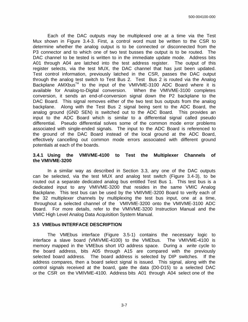
Each of the DAC outputs may be multiplexed one at a time via the TestMux shown in Figure 3.4-3. First, a control word must be written to the CSR todetermine whether the analog output is to be connected or disconnected from theP3 connector and to which one of two test busses the output is to be routed. TheDAC channel to be tested is written to in the immediate update mode. Address bitsA01 through A04 are latched into the test address register. The output of thisregister selects, via the test MUX, the DAC channel that has just been updated.Test control information, previously latched in the CSR, passes the DAC outputthrough the analog test switch to Test Bus 2. Test Bus 2 is routed via the AnalogBackplane AMXbusTM to the input of the VMIVME-3100 ADC Board where it isavailable for Analog-to-Digital conversion. When the VMIVME-3100 completesconversion, it sends an end-of-conversion signal down the P2 backplane to theDAC Board. This signal removes either of the two test bus outputs from the analogbackplane. Along with the Test Bus 2 signal being sent to the ADC Board, theanalog ground (GND SEN) is switched out to the ADC Board. This provides aninput to the ADC Board which is similar to a differential signal called pseudodifferential. Pseudo differential solves some of the common mode error problemsassociated with single-ended signals. The input to the ADC Board is referenced tothe ground of the DAC Board instead of the local ground at the ADC Board,effectively cancelling out common mode errors associated with different groundpotentials at each of the boards.
3.4.1 Using the VMIVME-4100 to Test the Multiplexer Channels ofthe VMIVME-3200
In a similar way as described in Section 3.3, any one of the DAC outputscan be selected, via the test MUX and analog test switch (Figure 3.4-3), to berouted out a separate dedicated analog bus entitled Test Bus 1. This test bus is adedicated input to any VMIVME-3200 that resides in the same VMIC AnalogBackplane. This test bus can be used by the VMIVME-3200 Board to verify each ofthe 32 multiplexer channels by multiplexing the test bus input, one at a time, throughout a selected channel of the VMIVME-3200 onto the VMIVME-3100 ADCBoard. For more details, refer to the VMIVME-3200 Instruction Manual and theVMIC High Level Analog Data Acquisition System Manual.
3.5 VMEbus INTERFACE DESCRIPTION
The VMEbus interface (Figure 3.5-1) contains the necessary logic tointerface a slave board (VMIVME-4100) to the VMEbus. The VMIVME-4100 ismemory mapped in the VMEbus short I/O address space. During a write cycle tothe board address, bits A05 through A15 are compared with the previouslyselected board address. The board address is selected by DIP switches. If theaddress compares, then a board select signal is issued. This signal, along with thecontrol signals received at the board, gate the data (D0-D15) to a selected DACor the CSR on the VMIVME-4100. Address bits A01 through A04 select one of the

A01
A02
A03
A04
TE
ST
A
DD
RE
SS
R
EG
IST
ER
DA
CH
AN
NE
L S
ELE
CT
1
TE
ST
RE
GIS
TE
R C
LOC
K
T
ES
T
MU
X
DA
O
UT
PU
TS
1
TO
16
MU
X
OU
T
1A
NA
LO
G
TE
ST
S
WIT
CH
4
TE
ST
CO
NT
RO
L
TE
ST
BU
S 1
TE
ST
BU
S 2
GN
D S
EN
P2
M41
00/F
3.4-
3
Fig
ure
3.4-
3. T
est B
us L
ogic
500-004100-000
3-8

500-004100-000
3-9
VMEbus CONNECTION
BOARD ADDRESS AND
ADDRESS MODIFIER
COMPARATORA15 to A05 AM5 to AM0
BOARD SELECT 1
A4 to A01 4
DAC CHANNEL ADDRESS
AND CONTROL REGISTER
DATA TRANSCEIVER
12 TO DACs
7
INTERNAL DATA BUS
21
16
D15 to D0
4
6
DAC ADDRESS
DA CONTROL
DATA TRANSCEIVER
DTACK GENERATOR
1
DTACK
5 3
P2 CONNECTOR
EXTERNAL DA TRIGGER
TEST BUS NO. 1
TEST BUS NO. 2
GND SEN
1 EXTERNAL DA TRIGGERTO DACs
M4100/F3.5-1
Figure 3.5-1. VMEbus Interface Logic and Interface Signals
4

500-004100-000
3-10
16 DAC channels when D15 is written low; data D0 through D11 is latched into theselected DAC. When D15 is written high to the board, then data D08 through D14is latched into the CSR.
The VMIVME-4100 circuitry requires +5V, +15V and -15V. The +5V issupplied to the board via the P1 and P2 connectors. An on-board DC-to-DCconverter generates the +15V and -15V for the analog circuitry, refer to Figure 3.5-2.
3.6 P2 CONNECTOR I/O SIGNAL DEFINITION
a. AINTESTBS (Test Bus 1). An analog test signal that originates fromthe DAC Board and is optionally used by the VMIVME-3200 MUXExpander Board to verify the multiplexer channels. Test Bus 1 maybe multiplexed through each channel of the VMIVME-3200 MUXBoard to a VMIVME-3100 ADC Board for conversion.
b. AOTESTBS (Test Bus 2). A second analog test bus from the DACBoard, used in conjunction with the VMIVME-3100 ADC Board toverify the 16 analog output channels of the DAC Board.
c. EXTSCL (External Start Convert - Low). An externally providedactive low input. When this line is input low, any word stored in theDAC first rank registers will begin analog conversion. To initiate aconversion, EXTSCL must go to a TTL low state for at least 150 nsbefore returning to a TTL high state. The board must have previouslybeen jumpered to enable the board to receive an external startconvert signal (see Section 5).
d. GND SEN. In test mode when Test Bus 2 is used, an analog groundfrom the DAC Board is routed out the GND SEN line. The GND SENline provides for a pseudo-differential input to a receiving ADC Board.

500-004100-000
3-11
P1
+5 V
GND
P2
+5 V
GND
DC-TO-DC CONVERTER
+5 V
GND -15 V
ANA COM
-15 V1
ANA COM
DC-TO-DC CONVERTER
+5 V
GND
-15 V
ANA COM
+15 V +15 V1
-15 V2
+5 V
DIG GND
M4100/F3.5-2
Figure 3.5-2. DAC Board Power

500-004100-000
4-1
SECTION 4
PROGRAMMING
4.1 INTRODUCTION
The Digital-to-Analog Converter (DAC) Board is memory mapped in theshort I/O address space. The board occupies 16 successive word locations in theVME short I/O address space of 65,535 bytes. The short I/O space is located fromFF0000 HEX to FFFFFF HEX. Each write or read cycle must be a word transfer toan even address, due to the DAC output resolution of 12 bits. The board baseaddress (XXXXX0 HEX) may be selected by DIP switches, as shown in Section5.5. Figure 4.1-1 represents the VMIVME-4100 address map, assuming the factoryset base address of FF0000 HEX. Note that the Control Status Register (CSR) canbe written to and read from any of the 16 word locations that the board occupies.When the board is written to, the destination of the data is controlled by data bit 15.If data bit 15 is a "one", the word is written to the control register; whereas, whendata bit 15 is a "zero", the data is written to the DAC which is addressed. Readingany address on the board will return the status of the board.
NOTE
JUMPER JB DETERMINES WHETHER THE BOARD OPERATES IN SHORTSUPERVISORY I/O ACCESS OR SHORT NON-PRIVILEGED I/O ACCESS. WITH THEJUMPER INSTALLED, SHORT NON-PROVILEGED I/O ACCESS IS SELECTED.
4.2 DAC BOARD PROGRAMMING OPTIONS
4.2.1 Introduction
There are two types of registers that must be written to for properoperation of the DAC Board. One is the CSR, the other is the DACs. The order inwhich they are written to may differ, depending on the desired mode of operationfor DAC channel start convert.
4.2.2 Immediate DAC Update Mode
The immediate DAC update mode is described in Section 3.1.1 and mustbe enabled by the jumper configuration described in Section 5.7. Once this hasbeen set up, a 12-bit word can be written to any DAC channel where it will beginimmediate analog conversion.

500-004100-000
4-2
CONTROL STATUS (READ/WRITE) ADDRESS
(MSB) (LSB)
D15 D14 D8 D7 D0
CONTROL STATUS BITS NOT USED1
FF0000FF0002
••
FF001E
DAC CHANNELS (0 TO 15) ADDRESS (WRITE ONLY)
(MSB) (LSB)
D15 D14 D12 D11 D0
NOT USEDNOT USEDNOT USEDNOT USEDNOT USEDNOT USEDNOT USEDNOT USEDNOT USEDNOT USEDNOT USEDNOT USEDNOT USEDNOT USEDNOT USEDNOT USED
0000000000000000
D13ADDRESS
DAC OUT 0DAC OUT 1DAC OUT 2DAC OUT 3DAC OUT 4DAC OUT 5DAC OUT 6DAC OUT 7DAC OUT 8DAC OUT 9DAC OUT 10DAC OUT 11DAC OUT 12DAC OUT 13DAC OUT 14DAC OUT 15
FF0000FF0002FF0004FF0006FF0008FF000AFF000CFF000EFF0010FF0012FF0014FF0016FF0018FF001AFF001CFF001E
M4100/F4.1-1
Figure 4.1-1. Control Status Register and DAC Channels Address Map

500-004100-000
4-3
By the operation of the CSR and its control of the analog isolationswitches between the DAC outputs and the P3 (user) connector, all 16 DACchannels can be initiated to the proper value as described in the precedingparagraph. After powering up the board, load the DAC channels with the initial 12-bit word (positive-true offset binary coding, Table 4.2.2-1) required. A control wordcan then be written to the CSR to enable the DAC outputs to the P3 connector. TheCSR bit description for this mode of operation is detailed in Tables 4.2.2-2 and4.2.2-3. A programming example of the immediate DAC update mode is detailed inSection 4.5.
4.3 DELAYED DAC UPDATE MODE
The delayed DAC update mode operation is described in Section 3.2.This mode must have previously been enabled by the jumper configuration givenin Section 5.7. There are two ways for a DAC channel to be updated after the 12-bit word is loaded into the DACs first register. The first, is under program controlwhen data bit D9 is written high to the CSR. Data bit D15 must always be highwhen writing to the CSR. It should be noted that when setting D9 to initiate theDAC update, control bits D8 and D10 through D14 should be set or reset accordingto where the user wants the converted output to be routed (refer to Tables 4.2.2-2 and4.2.2-3). Also, a previously loaded DAC may be updated by an externaltrigger input from another device. A programming example of the delayed DACupdate mode is detailed in Section 4.6.
4.4 TEST MODE PROGRAMMING
As described in Section 3.3, any of the 16 DAC outputs may be selectedto pass to a VMIVME-3100 ADC Board over Test Bus 2 to verify the DAC outputs. Ifa VMIVME-3200 is present in the analog backplane, then any DAC output can beselected to go to that board for test purposes over Test Bus 1. Generally, theprogramming sequence for utilizing one of the two test busses is as follows:
If immediate DAC update mode is employed, then a control word shouldbe written to the CSR. In this control word, information is included as to which testbus the DAC output is to be routed and whether the output is to be isolated orconnected to the P3 connectors (refer to Tables 4.2.2-2 and 4.2.2-3). The DAC tobe updated is then loaded with a 12-bit word. The channel is updated and passesout the selected test bus.
An output may be also updated under program control to route to aspecified test bus. The board must have previously been jumpered toaccommodate the delayed DAC update mode, as shown in Section 5.7. Theprogramming sequence is as follows:

500-004100-000
4-4
Table 4.2.2-1. DAC Data Format Analog Output vs Digital Input (±10 V Scale)
DIGITAL INPUT CODE
ANALOG OUTPUT VOLTAGE(MSB) (LSB)D15 D00XXX 0XXX0XXX0XXX0XXX0XXX
0000 0100 1000 0000 1100 1111
0000 0000 0000 0000 0000 1111
0000 0000 0000 0001 0000 1111
-10.000 V -5.000 V 0.000 V 4.88 mV +5.000 V 9.9951V
-FULL SCALE -1/2 SCALE ZERO +1 LSB +1/2 SCALE +FULL SCALE - 1 LSB
The analog output may be calculated by the input code written by theprocessor to the selected DAC channel as follows:
Analog Output = -10 V + (Digital Input Code in Decimal)X __20__
4096Example: The Analog output for a digital input of 0A00H would be:
(1) 0A00H decimal equivalent is 2560(2) Analog Out = -10 V + (2560) __20__
4096
= 2.5
M4100/T4.2.2-1

500-004100-000
4-5
Table 4.2.2-2. Control Register Data Format and Definitions
D15 D14 D13 D12 D11 D10 D09 D08 D07 D00
1 NOT USED
D08 When written high, engages DAC outputs to the P3 connector, and disengages DAC outputs from P3 connector when written low. At power-up, this control bit is low.
D09 Program Control Start Convert, when input high, generates a signal thattransfers contents of previously loaded DACs to the second rank register andupdates the analog ouput.
D10 In test mode, written high to clock channel address bits A01 through A04 intotest register to select one of 16 DAC channel outputs. Used in conjunctionwith D11, D12 and D13 to determine test modes.
D11 When written high, engages analog outputs from DAC to one of two testbusses. Used in conjunction with D12 and D13 to determine which test busis selected. At power up, this control bit is low which disengages the testbusses.
D12 A high state enables the selected test analog output to pass out the P2 connector on Test Bus 1 (AINTESTBS). At power up this control bit is low.
D13 A high state enables the selected test analog output to pass out the P2connector on Test Bus 2 (AOTESTBS). At power up this control bit is low.
D14 A low state turns the Fail LED ON. A high state turns it OFF. At power up,this control bit is low.
D15 This bit is used as a register select bit to determine which type of device is tobe selected during a write cycle. D15 must be high when writing to thecontrol register. Otherwise, D15 is low when writing to the DAC channels.
M4100/T4.2.2-2

500-004100-000
4-6
Programming the CSR for Different Analog Output Variations - Bit Definitions
Table 4.2.2-3.
Analog output over TEST BUS 1 (AINTESTBS).1.
D15 D14 D13 D12 D11 D10 D09 D08
1 1 0 1 1 10 or 1*
0
Analog output over TEST BUS 2 (AOTESTBS).2.
D15 D14 D13 D12 D11 D10 D09 D08
1 1 1 0 1 10 or 1*
0
Analog output out TEST BUS 2 and out P3 connector to field connected device (used for real-time fault detection of DACs).
3.
D15 D14 D13 D12 D11 D10 D09 D08
1 1 1 0 1 10 or 1*
1
Analog output over P3 connector only.4.
D15 D14 D13 D12 D11 D10 D09 D08
1 1 0 0 0 00 or 1*
1
M4100/T4.2.2-3
*See Table 4.2.2-2.

500-004100-000
4-7
First, a 12-bit word is written to the address of the DAC channel that is tobe updated. The data is stored in the DAC register and will be converted by settingthe proper bits in a write cycle to the CSR. The CSR must be written to at the sameaddress as that of the DAC channel that has previously been loaded. Thedifference being that data bit D15 must be a "zero" when writing to the DACchannel register and a "one" when writing to the CSR. Data bit D09, when writtenas "one" to the CSR, initiates the analog conversion of the previously stored 12-bitword.
The test modes can only be used if a VMIVME-3100 ADC Board exists inthe same VMIC Analog (P2) Backplane (AMXbusTM) as the VMIVME-4100.
4.5 MC68000 ASSEMBLY LANGUAGE PROGRAMMING OF THEVMIVME-4100 DAC BOARD
Only a few assembly language statements are necessary to properlycontrol and utilize the DAC board. It will be assumed that the base address of theboard in this example is FF0060H. The board address can be determined byinformation given in Sections 4.1 and 5.5.
The first example will be the loading of all the 16 DACs with a full scalevalue of FFFH, giving an analog output over the P3 connector of 9.9951 volts. TheDAC output value will be updated immediately upon being written to. This is theimmediate DAC update mode explained in Section 4.1.2. The following program isintended as an instructional example only and may not be useful in the user’sapplication. To enable the DAC immediate update mode, the jumper configurationgiven in Section 5.7 must be employed. A flow chart of this example is shown inFigure 4.5-1, and the assembly language program is shown in Figure 4.5-2.
4.6 PROGRAM EXAMPLE (DELAYED DAC UPDATE MODE)
In the programming example in Section 4.4, all 16 DACs were loadedwith a full scale value of FFFH in the immediate update mode. For illustrationpurposes, the same result will be obtained by this programming example by usingthe delayed DAC update mode. The delayed DAC mode is jumper selectable, asdescribed in Section 5.7. The flow chart in Figure 4.6-1 shows the programmingsequence and example program listing, and comments are shown in Figure 4.6-2.A base address of FF0060H is assumed.
In the following program example, all 16 DAC channels are loaded withnew data then updated under program control. Alternatively, if previously enabled,an external trigger input could have initiated the DA conversion process.

500-004100-000
4-8
POWER-UP (ON-BOARD
INITIALIZATION)
INITIALIZE DAC ADDRESS
POINTER
LOAD DAC CONTROL REGISTER
LOAD DAC
HAVE ALL 16 DAC
CHANNELS BEEN UPDATED
?
NO
YES
END M4100/F4.5-1
Figure 4.5-1. DAC Programming Sequence (Immediate DAC Start Convert Mode)

500-004100-000
4-9
COMMENT MOVE.W #$ 0, D0 1MOVE.W #C100H,$FF0060 2LEA $ FF0060, A0 3
LOAD NEXT DA MOVE.W #$ 0FFF, (A0)+ 4ADD.W #1, D0 5CMP.W #$ 0010, D0 6BNE LOAD NEXT DA 7STOP 8
COMMENTS:
1. Initialize register D0 (used as a counter) to 0.
2. Load control register (D15 must be a 1) to enable analog outputs to P3 connector.
3. Load address of DAC Channel no. 1 into address register A0
4. Load DAC channel with maximum value. Address pointer is automaticallyincremented to next DAC channel.
5. Increment counter stored in D0.
6. If all 16 DAC channels have not been loaded, then go to step 7.
7. Load next DAC channel.
8. STOP
In step 2, the control register was set to enable the analog outputs overthe P3 connector. The outputs could have also been selected to pass out either ofthe two test busses, or out the AOTESTBS and the P3 connector simultaneously byselecting the proper control word as determined from Table 4.2.2-3 and the HEXvalue for the different control words shown in Table 4.5-1.
M4100/F4.5-2
Figure 4.5-2. Program Example (Immediate DAC Update Mode)
Table 4.5-1. Analog Output Control in Immediate Update Mode
ANALOG OUT PATHWAY CONTROL WORD (D15 TO D0) HEX VALUE
P3 CONNECTOR C100AOTESTBS (TEST BUS 2) EC00AINTESTBS (TEST BUS 1) DC00AOTESTBS & P3 CONNECTOR ED00
M4100/T4.5-1

500-004100-000
4-10
POWER-UP (ON-BOARD
INITIALIZATION)
HAVE
ALL 16 DAC
CHANNELS BEEN
UPDATED
?
NO
YES
LOAD DAC CONTROL REGISTER
Figure 4.6-1. DAC Programming Sequence (Delayed DAC Update Mode)
INITIALIZE DAC ADDRESS
POINTER
LOAD DAC
END
M4100/F4.6-1

500-004100-000
4-11
COMMENT MOVE.W #$ 0, D0 1LEA $ FF0060, A0 2
LOAD NEXT DAC MOVE.W #$ 0FFF, (A0)+ 3ADD.W #1, D0 4CMP.W #$ 0010, D0 5BNE LOAD NEXT D/A 6MOVE.W #$ C300, $FF0060 7STOP 8
COMMENTS:
1. Initialize register D0 (used as a counter) to 0.
2. Load address of DAC Channel no. 1 into address register A0.
3. Load DAC channel with maximum value. Address pointer is automaticallyincremented to next DAC channel.
4. Increment counter stored in D0.
5. If all 16 DAC channels have not been loaded, then go to step 6.
6. Load next DAC channel.
7. Load control register to start digital-to-analog conversion of all 16 DACchannels. Analog outputs are routed out P3 connector.
8. STOP
In step 7, the control register was set to enable the analog outputs topass out the P3 connector. The outputs could have also been selected to pass outeither of the two test busses or out the AOTESTBS (Test Bus 2) and the P3connector simultaneously by selecting the proper control word as determined fromTable 4.1-3 and the HEX value for the different control words shown below in Table4.6-1.
M4100/F4.6-2
Figure 4.6-2. Program Example (Delayed DAC Update Mode)
Table 4.6-1. Analog Output Control in the Delayed DAC Update Mode
ANALOG OUT PATHWAY CONTROL WORD (D15 TO D0) HEX VALUE
P3 CONNECTOR C300AOTESTBS (TEST BUS 2) EE00AINTESTBS (TEST BUS 1) DE00AOTESTBS & P3 CONNECTOR EF00
M4100/T4.6-1

500-004100-000
5-1
SECTION 5
CONFIGURATION AND INSTALLATION
5.1 UNPACKING PROCEDURES
CAUTION
SOME OF THE COMPONENTS ASSEMBLED ON VMIC’S PRODUCTS MAY BESENSITIVE TO ELECTROSTATIC DISCHARGE AND DAMAGE MAY OCCUR ONBOARDS THAT ARE SUBJECTED TO A HIGH ENERGY ELECTROSTATIC FIELD.UNUSED BOARDS SHOULD BE STORED IN THE SAME PROTECTIVE BOXES INWHICH THEY WERE SHIPPED. WHEN THE BOARD IS TO BE LAID ON A BENCHFOR CONFIGURING, etc., IT IS SUGGESTED THAT CONDUCTIVE MATERIAL BEINSERTED UNDER THE BOARD TO PROVIDE A CONDUCTIVE SHUNT.
Upon receipt, any precautions found in the shipping container should beobserved. All items should be carefully unpacked and thoroughly inspected fordamage that might have occurred during shipment. The board(s) should bechecked for broken components, damaged printed-circuit board(s), heat damage,and other visible contamination. All claims arising from shipping damage shouldbe filed with the carrier and a complete report sent to VMIC, together with a requestfor advice concerning disposition of the damaged item(s).
5.2 PHYSICAL INSTALLATION
CAUTION
DO NOT INSTALL OR REMOVE BOARDS WHILE POWER IS APPLIED.
To install the board, de-energize the equipment and insert the board intoan appropriate slot of the chassis, while ensuring that the card is properly alignedand oriented in the supporting card guides. Slide the card smoothly forwardagainst the mating connector until firmly seated. Review Sections 5.3 and 5.4before operating the board.
5.3 INSTALLATION
This section describes the VMIVME-4100 Digital-to-Analog Converter(DAC) Board setup procedure and jumper configuration. The board select baseaddress and board jumper configuration are factory preset and are shown in Table5.3-1. The base address selection switches (S1 and S2) are all shown in thefactory configured position. This implies a base address for the board at FF0060H.

500-004100-000
5-2
Table 5.3-1. VMIVME-4100 Factory Set Jumpers and Address SwitchConfigurations
JUMPER FUNCTION PRESET CONDITION
S1 BASE ADDRESS SELECTION SWITCH(A05, A06)
S2 BASE ADDRESS SELECTION SWITCH(A15 TO A07)
JA
JB
NOT USER SELECTABLE
DETERMINES ADDRESS MODIFIERRESPONSE OF THE BOARD.JUMPER NOT INSTALLED INDICATESRESPONSE TO SHORT SUPER-VISORY I/O ACCESS
JC
JC JUMPERS 1 TO 4 DETERMINE DACUPDATE MODE. FACTORY PRESETTO IMMEDIATE DAC UPDATE MODE.JC JUMPER 5 ENABLES/DISABLESDAC EXTERNAL TRIGGER. FACTORYPRESET TO DISABLE EXTERNALJUMPER
A05 A06 not used
ON = 0
OFF = 1
A15 A07ON
OFF
JB
NOTINSTALLED
AT FACTORY
1 2 3 4 5
JC
NO JUMPERS INSTALLEDAT FACTORY
M4100/T5.3-1
5.4 BEFORE APPLYING POWER: CHECKLIST
Before installing the board in a VMEbus system, go through the followingchecklist to verify the board is ready for the intended operation:
1. Have the sections on Theory and Programming of the DAC Board,Sections 3.0 and 4.0, been read and applied to system requirements?
__√___
2. Review Table 5.3-1 to verify the factory installed jumpers and boardaddress select switches are set to desired positions. _______

500-004100-000
5-3
a. To change DAC Board Address Switches (S1 and S2) see
Section 5.5.b. To change address modifier response jumper (JB), see Section
5.6.c. To change DAC update mode jumpers JC 1 to 4, see Section 5.7.d. To change enable/disable DAC external trigger jumper JC-5, see
Section 5.8.
3. To calibrate the +10 V precision reference, see Section 5.9 _______ 4. Has the cable, with proper mating connector, been connected to the
analog output connector (P3)? See Section 5.10. _______
5. When optional output isolation hardware is employed on theVMIVME-4100, review Section 5.11 for load impedance requirement.
_______
5.4.1 DAC Board Installation
After steps 1 through 5 have been reviewed in Section 5.4, then the DACBoard may be installed in a VMEbus system (do not install or remove theboard with power ON). The DAC Board may generally be installed in any slotposition, except slot one which is usually reserved for the master processing unit.
5.5 BOARD ADDRESS SELECTION-SWITCHES
There are two address select DIP switches on board the VMIVME-4100board. Each individual switch corresponds to an address bit or is not used. If theswitch is ON, the corresponding address bit is compared to a logic "zero". Allcorresponding address bits must compare with the switch positions during awrite/read of the DAC Board. The way in which each switch corresponds to theaddress bits is shown in Figure 5.5-1. See Figure 5.5-2 for switch locations on theboard.
5.6 ADDRESS MODIFIER RESPONSE SELECTION
The DAC Board is memory mapped in the short I/O address space, asdescribed previously in Section 4.1. The DAC Board will respond to either of thetwo address modifier codes that may be issued to the DAC Board by a CPU boardduring a write or read cycle. The DAC Board is factory set to respond tosupervisory short I/O access. To select non-privilege short I/O access, install thejumper installed at jumper location (JB). See Figure 5.5-2 for jumper location onthe board.

500-004100-000
5-4
ON, CLOSED = 0
OFF, OPEN = 11 2 3 4 5 6 7 8
A15 A14 A13 A12 A11 A10 A09 A08
S2
1 2 3 4S1
A05 A06 (NOT USED)
9
A07
For the VMIVME-4100 to respond to a base address of (FFFF00) the S1 andS2 switches would be set accordingly.
16
1 2 3 4 5 6 7 8
OFF OFF OFF OFF OFF OFF OFF
ON ON X X
S2
S1
9
OFF ON
Figure 5.5-1. Base Address DIP Switch Setup
M4100/F5.5-1

+10
VO
LT
PR
EC
ISIO
N
RE
FE
RE
NC
E
AD
JUS
TM
EN
T
P2R6
BA
SE
AD
DR
ES
S
SE
LEC
TIO
N
SW
ITC
HE
S
JB
AD
DR
ES
S
MO
DIF
IER
JU
MP
ER
S2
P1
P3
S1
JC
DA
C U
PD
AT
E M
OD
E
JUM
PE
RS
AN
D D
AC
E
XT
ER
NA
L T
RIG
GE
R
JUM
PE
R
1 2
3 4
5
3
Fig
ure
5.5-
2. J
umpe
r an
d S
witc
h Lo
catio
ns o
n V
MIV
ME
-410
0 (C
ompo
nent
Sid
e S
how
n)
VM
IVM
E-4
100
M41
00/F
5.5-
2
500-004100-000
5-5

500-004100-000
5-6
5.7 DAC UPDATE MODE SELECT JUMPERS
There are four jumpers and each jumper corresponds to a set of fourDAC channels. To enable a set of channels for the immediate DAC update mode,the corresponding jumper is removed (not installed). If a jumper is installed, thenthat set of four channels will operate in the delayed DAC update mode. Jumperlocation (JC) is shown in Figure 5.7-1.
DAC Channels 1 to 4 - Install Jumper JC-1DAC Channels 5 to 8 - Install Jumper JC-2DAC Channels 9 to 12 - Install Jumper JC-3DAC Channels 13 to 16 - Install Jumper JC-4
1 2 3 4 5
JC
M4100/F5.7-1
Figure 5.7-1. Jumper Configuration
5.8 EXTERNAL DAC UPDATE TRIGGER ENABLE/DISABLE
Install jumper JC-5 if external trigger operation is desired. Otherwise,remove jumper JC-5. See Figure 5.7-1 for jumper locations on board.
5.9 CALIBRATING THE +10 VOLT PRECISION REFERENCE
The +10 V precision reference has been adjusted at the factory and lock-tight has been applied to the potentiometer adjustment to insure no changes inshipping and handling. However, the lock-tight is easily broken away for useradjustment if necessary. Long-term drift of the reference is very low (0.25 mV/1000hrs). It is advised that after 6,000 hours of operation, or if the reference output (P2connector) is being used by other devices, that the reference voltage be checkedwith a 5-1/2 digit voltmeter. The procedure is as follows:

500-004100-000
5-7
a. Remove any cable connected to the P3 connector.
b. Apply power to the board and let warm up 15 minutes.
c. Attach the negative lead of the voltmeter to the P3 connector pin C-1.
d. Attach the positive lead of the voltmeter to the jumper JD pin 2 wirejumper (see Figure 5.5-2 for board location of jumper JD).
e. If voltage is not within 1.0 mV of +10 V, then re-calibrate reference.
f. Re-calibrate reference by adjusting potentiometer R6 (board locationshown in Figure 5.5-2) to +10 V(± 0.5 mV).
5.10 CONNECTOR DESCRIPTIONS
Two connectors, P1 and P2, connect the DAC Board to the VMEbusbackplane. The connectors are 96-Pin DIN type. The primary connector, P1,contains the address data and control lines, and all additional signals necessary tocontrol data transfer and other bus functions. P2 connector carries the I/O linesnecessary to join the DAC Board with the optional VMIVME-3200 MUX ExpanderBoard and the VMIVME-3100 12-Bit Analog-to-Digital Converter (ADC) Board. TheP2 connector connects the DAC Board with the Analog P2 Backplane (AMXbus™).See Figure 5.10-1 for P2 pin and signal assignments.
If the test bus option is to be used in conjunction with other VMIC AnalogInput/Output (AIO) Boards, then the user must use a VMIC printed circuit Analog P2Backplane (AMXbus™). These backplanes are available in different slot widths toaccommodate almost any combination of boards.
The P3 connector is a Panduit 32-pin male connector type120-332-033A. The matching Panduit connector for the input cable is a femaleconnector type 120-332-435E. This connector handles 16 analog outputs each,with an associated analog ground wire. See Figure 5.10-2 for P3 connector pinand signal assignments.
5.11 ANALOG OUTPUT ACCURACY WHEN OPTIONAL OUTPUTISOLATION HARDWARE IS USED
The VMIVME-4100 is offered in several option configurations to the user.One of which is the use of Built-in-Test functions when used with other VMIVMEboards as discussed previously in Section 3.3.

500-004100-000
5-8
AC
REAR VIEW OF BOARD
ROW
B
32
31
30
29
28
27
26
25
24
23
22
21
20
19
18
17
16
15
14
13
12
11
10
9
8
7
6
5
4
3
2
PIN 1
PC BOARD
M4100/F5.10-1
Figure 5.10-1. P2 Connector - Pin Assignments
PIN NUMBERROW AROW BROW C
GND
EXTSCL
ANA COM
ANA COM
ANA COM
ANA COM
ANA COM
+10 V REF
ANA COM
GND SEN
ANA COM
ANA COM
ANA COM
AOTESTBS
ANA COM
AINTESTBS
ANA COM
ANA COM
ANA COM
ANA COM
ANA COM
ANA COM+5 V
GND
GND
+5 V
GND
+5 V

500-004100-000
5-9
16
15
14
13
12
11
10
9
8
7
6
5
4
3
2
1
A C
FRONT VIEW OF P3
CONNECTOR
ROW
Figure 5.10-2. P3 Connector - Pin Assignments
M4100/F5.10-2
PIN NUMBERROW AROW BROW C
AN15
AN14
AN13
AN12
AN11
AN10
AN09
AN08
AN07
AN06
AN05
AN04
AN03
AN02
AN01
AN00
ANA COM
ANA COM
ANA COM
ANA COM
ANA COM
ANA COM
ANA COM
ANA COM
ANA COM
ANA COM
ANA COM
ANA COM
ANA COM
ANA COM
ANA COM
ANA COM
P.C. BOARD

500-004100-000
5-10
The Built-in-Test hardware features analog output isolation switches forall 16 channels that can be turned OF/OFF by software commands. Theseswitches are in series with the analog output and the user-connected device at theP3 connector. These switches have an ON resistance of approximately 100 ohms(max). If the user-connected load does not have a high impedance input, then apossible voltage division error is introduced. For example, if R(LOAD) is 10 kΩ,then a 1% error is introduced. R(LOAD) should be one megohm or greater for anerror of .01% or less.

500-004100-000
6-1
SECTION 6
MAINTENANCE AND WARRANTY
6.1 MAINTENANCE
This section of the technical manual provides information relative to thecare and maintenance of VMIC’s products. Should the products malfunction, theuser should verify the following:
a. Softwareb. System configurationc. Electrical connectionsd. Jumper or configuration optionse. Boards fully inserted into their proper connector locationf. Connector pins are clean and free from contaminationg. No components of adjacent boards are disturbed when inserting or
removing the board from the VMEbus card cageh. Quality of cables and I/O connections
User level repairs are not recommended. Contact VMIC for a ReturnMaterial Authorization (RMA) Number. This RMA Number must be obtained prior toany return.
6.2 MAINTENANCE PRINTS
The appendix(ices) to this manual contain(s) drawings and diagrams forreference purposes.
6.3 WARRANTY
VMIC’s Standard Products are warranted to be free from defects inmaterial and workmanship for a period of two years (24 months) from the date ofshipment. In discharge of this warranty, VMIC, at its option, agrees to either repairor replace, at VMIC’s facility and at VMIC’s discretion, any part, component,subassembly accessory, or any hardware, software, or system product, whichunder proper and normal use proves defective in material and workmanship.
The customer shall provide notice to VMIC of each such defect within areasonable time after the customer’s discovery of such defect.
In order to return the defective product(s) or part(s), the customer mustcontact VMIC’s Customer Service Department to obtain a Call Ticket Number. The

500-004100-000
6-2
defective product(s) or part(s) must also be properly boxed and weighed. After aVMIC Call Ticket Number and RMA Number have been obtained, the defectiveproduct(s) or part(s) may be returned (transportation collect for surface UPS) toVMIC. Any replaced or repaired product(s) or part(s) will be shipped back to thecustomer’s at the expense of VMIC (also UPS surface).
The customer should be aware that the above process can sometimestake up to eight (8) days for the shipment to reach VMIC. The customer has theoption to ship the defective product(s) or part(s) at the customer’s own expense ifthe customer cannot afford this possible delay.
There shall be no warranty or liability on any VMIC product(s) or part(s)that is (are) damaged or subjected to accident(s), perils of nature, negligence,overtemperature, overvoltage, misapplication of electrical power, insertion orremoval of boards from backplanes and/or I/O connectors with power applied bythe customer(s), appointee(s), or any other person(s) without the expressedapproval of VMIC.
Final determination of warranty eligibility shall be made by VMIC, and if awarranty claim is considered invalid for any reason, the customer will be chargedfor services performed and expenses incurred by VMIC in repair, handling andshipping the returned product or part. Determination as to whether the item iswithin warranty, coverage shall not be unreasonably withheld.
The warranty period of the replacement or repaired product(s) or part(s)shall terminate with the termination of the warranty period with respect to theoriginal product(s) or part(s) for all replacement parts supplied or repairs madeduring the original warranty period.
THE FOREGOING WARRANTY AND REMEDY ARE EXCLUSIVE AND VMICSHALL HAVE NO OTHER OR ADDITIONAL LIABILITY TO BUYER OR TO ANYONECLAIMING UNDER BUYER (THIRD PARTY) UNDER ANY OTHER AGREEMENT ORWARRANTY, EXPRESS OR IMPLIED EITHER IN FACT OR BY OPERATION OF THELAW, INCLUDING ANY IMPLIED WARRANTY OF MERCHANTABILITY OR FITNESS,STATUTORY, OR OTHERWISE. VMIC SHALL HAVE NO LIABILITY FOR SPECIALOR CONSEQUENTIAL DAMAGES OF ANY KIND OR FROM ANY CAUSE ARISINGOUT OF THE INSTALLATION OR USE OF ANY PRODUCT FURNISHEDHEREUNDER.
6.4 OUT-OF-WARRANTY REPAIR POLICY
The following sections describe VMIC’s policy on repairs and warrantieson repaired products.

500-004100-000
6-3
6.4.1 Repair Category
VMIC’s repair policy of standard products is divided into two categories,depending on the item to be repaired. These categories are:
a. Product Exchangeb. Fixed Price Repair
Category 1 (product exchange) represents the fastest turn around of thetwo categories. In this case, the customer sends the malfunctioning product toVMIC. VMIC will return an operational product to the customer within 72 hours ofreceipt provided VMIC has the product in stock.
Provided that the returned product is repairable customers shouldcontact VMIC prior to returning products for repair to determine stocking status.
Category 2 (Fixed Price Repair) applies to products returned to VMIC forrepair and subsequent return to the customer.
Return authorizations are required on all product repairs, and allpurchase orders should refer to VMIC’s RMA Number which is assigned by VMIC’sCustomer Service Department.
6.4.2 Repair Pricing
Contact your factory representative for repair pricing. Current pricing canbe found in the Repair and Replacement Policy in the most current StandardConditions of Sales Document (F0109-91). Refer to exclusions (Section 6.4.7).
6.4.3 Payment
Payment is due upon delivery or at VMIC’s option, net thirty (30) daysfrom the date of delivery. Payment should be made to:
VME Microsystems International Corporation12090 South Memorial ParkwayHuntsville, Alabama 35803-3308Attention: Accounts Receivable
VMIC allows a one (1) percent discount for payment made within ten (10)days of invoice date or a two (2) percent discount on payment made prior toshipment of order. This payment discount, however, does not apply to freight.

500-004100-000
6-4
6.4.4 Shipping Charges
Shipping charges are the customer’s responsibility, with the exception ofwarranty repairs, whereby VMIC will pay the return to customer shipping charges.
6.4.5 Shipping Instructions
The type of packaging used to ship the product depends on whether theproduct is shipped singly, in a chassis, or packaged with other boards. Theshipper should carefully pack the product(s), using the same precautions listed inthe "unpacking procedures". The user should utilize the same (or equivalent)protective packaging container for re-shipment as provided by VMIC. ApprovedESD procedures are recommended when handling VMIC’s products.
6.4.6 Warranty on Repairs
Products repaired by VMIC are warranted against defects inworkmanship and material for a period of ninety (90) days from date of shipment tothe customer for all products that were repaired out of warranty. See StandardConditions of Sale for products repaired within the warranty.
6.4.7 Exclusions
Repair rates may not apply to products which have received unusualphysical or electrical damage. In such cases, VMIC will provide an estimated pricefor product repair or replacement. The customer may then choose to have theproduct repaired at the estimated price, returned unrepaired at no charge, orreplaced at VMIC’s current list price.

APPENDIX A
ASSEMBLY DRAWING, PARTS LIST,AND SCHEMATIC

DOCUMENTATION EVALUATION FORM
VMIC welcomes your comments and suggestions.
Please return this form to: VME MICROSYSTEMS INTERNATIONAL CORPORATION 12090 South Memorial Parkway Huntsville, Alabama 35803-3308 (205) 880-0444 1-800-322-3616
Evaluation: Please rate the following areas on a scale of 1 to 5 (1 = Poor; 5 = Excellent).
DOCUMENT NO.: __________________________________REVISION DATE: __________________________________
READABILITY ________ ILLUSTRATIONS ________
ORGANIZATION ________ PROGRAMMING INFORMATION ________
ACCURACY ________ SPECIFICATIONS ________
COMPLETENESS ________ MAINTENANCE DIAGRAMS ________
SPECIFIC PROBLEMS: PAGE(s)
( ) CLARIFICATION REQUIRED __________
( ) NOT ENOUGH INFORMATION GIVEN __________
( ) TYPOGRAPHICAL ERRORS __________
( ) TECHNICAL ERRORS(EXPLAIN): ____________________________________________
__________________________________________________________________________
DOCUMENT USE: (check all that apply)( ) HARDWARE ( ) SOFTWARE ( ) PRODUCT EVALUATION( ) OPERATION ( ) MAINTENANCE ( ) TRAINING
ADDITIONAL COMMENTS: _________________________________________________________________________________________________________________________________________________________________________________________________________________________________________________________________________________
YOUR NAME: ________________________________
TITLE: ________________________________
COMPANY: ________________________________
MAIL STOP: ________________________________
STREET: ________________________________
CITY, STATE, ZIP: ________________________________
PHONE: ________________________________