vs10xx - application notes
TRANSCRIPT
VLSISolution y VS10XX APPL. NOTES
VS1001K, VS1011, VS1002D
VS10XX - APPLICATION NOTES
Features• Quick Startup
• Saving I/O Pins
• MP3 Player
• ESD Protection
• Highest SPI Speed
• ADPCM Recording
• SPI Boot Format
Description
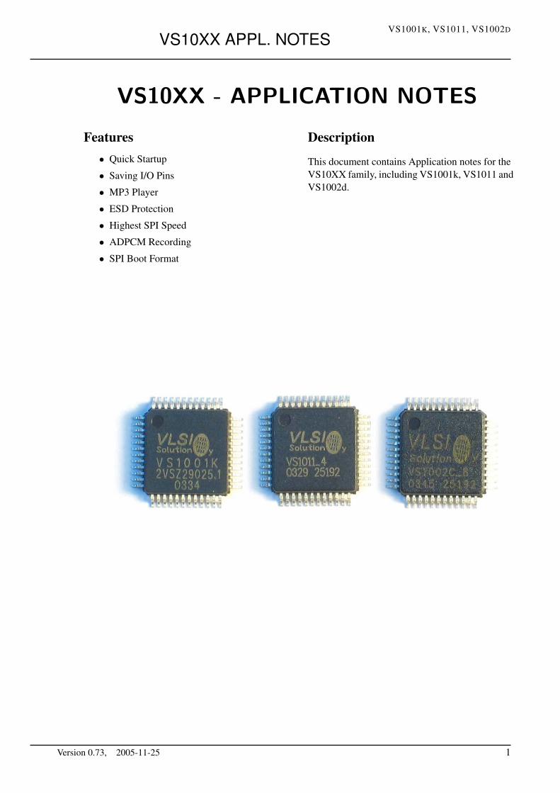
This document contains Application notes for theVS10XX family, including VS1001k, VS1011 andVS1002d.
Version 0.73, 2005-11-25 1
VLSISolution y VS10XX APPL. NOTES
VS1001K, VS1011, VS1002D
CONTENTS
Contents
1 Introduction 7
1.1 Definitions . . . . . . . . . . . . . . . . . . . . . . . . . . . . . . . . . . . . . . . . . . 7
1.2 Conventions . . . . . . . . . . . . . . . . . . . . . . . . . . . . . . . . . . . . . . . . . 7
2 General Hints (all) 8
2.1 Short-Circuiting Analog Outputs (all) . . . . . . . . . . . . . . . . . . . . . . . . . . . 8
2.2 Using an External Clock (all) . . . . . . . . . . . . . . . . . . . . . . . . . . . . . . . . 8
2.3 Application Programs (11, 02) . . . . . . . . . . . . . . . . . . . . . . . . . . . . . . . 8
2.4 Application Programs (01) . . . . . . . . . . . . . . . . . . . . . . . . . . . . . . . . . 9
3 Clock Speeds (all) 11
3.1 General (all) . . . . . . . . . . . . . . . . . . . . . . . . . . . . . . . . . . . . . . . . . 11
3.2 Maximum Sample Rate (all) . . . . . . . . . . . . . . . . . . . . . . . . . . . . . . . . 11
3.3 Maximum Amount of DSP Effects (all) . . . . . . . . . . . . . . . . . . . . . . . . . . 11
3.4 Maximum Decodable Bitstream (all) . . . . . . . . . . . . . . . . . . . . . . . . . . . . 12
3.4.1 CLKI = 12.288 MHz (all) . . . . . . . . . . . . . . . . . . . . . . . . . . . . . 12
3.4.2 CLKI = 22.580 MHz (all) . . . . . . . . . . . . . . . . . . . . . . . . . . . . . 12
3.4.3 CLKI = 24.576 MHz (all) . . . . . . . . . . . . . . . . . . . . . . . . . . . . . 12
3.4.4 CLKI = 26.000 MHz (all) . . . . . . . . . . . . . . . . . . . . . . . . . . . . . 12
3.4.5 CLKI = 28.000 MHz (all) . . . . . . . . . . . . . . . . . . . . . . . . . . . . . 12
4 Quick Startup (all) 13
4.1 Overview (all) . . . . . . . . . . . . . . . . . . . . . . . . . . . . . . . . . . . . . . . . 13
4.2 Seeing If Analog Works (all) . . . . . . . . . . . . . . . . . . . . . . . . . . . . . . . . 13
4.3 Seeing If Firmware Wakes Up (all) . . . . . . . . . . . . . . . . . . . . . . . . . . . . . 13
Version 0.73, 2005-11-25 2
VLSISolution y VS10XX APPL. NOTES
VS1001K, VS1011, VS1002D
CONTENTS
4.4 Writing to SCI (11, 02) . . . . . . . . . . . . . . . . . . . . . . . . . . . . . . . . . . . 13
4.5 Writing to SCI (01) . . . . . . . . . . . . . . . . . . . . . . . . . . . . . . . . . . . . . 14
4.6 Reading from SCI (all) . . . . . . . . . . . . . . . . . . . . . . . . . . . . . . . . . . . 14
4.7 Writing to SDI (01; 11’s and 02’s compatibility mode) . . . . . . . . . . . . . . . . . . 14
4.8 Writing to SDI (11’s and 02’s new mode) . . . . . . . . . . . . . . . . . . . . . . . . . 15
5 How to Play a Song (11, 02) 16
6 Saving I/O Pins (11, 02) 17
6.1 Overview (11, 02) . . . . . . . . . . . . . . . . . . . . . . . . . . . . . . . . . . . . . . 17
6.2 SPI With Other Devices Connected (11, 02) . . . . . . . . . . . . . . . . . . . . . . . . 17
6.3 SPI With VS10XX As the Only Device (11, 02) . . . . . . . . . . . . . . . . . . . . . . 18
7 Saving I/O Pins (01) 19
7.1 Overview (01) . . . . . . . . . . . . . . . . . . . . . . . . . . . . . . . . . . . . . . . . 19
7.2 Prerequirements (01) . . . . . . . . . . . . . . . . . . . . . . . . . . . . . . . . . . . . 19
7.3 Using the Connection (01) . . . . . . . . . . . . . . . . . . . . . . . . . . . . . . . . . 19
7.3.1 Selecting the Right Chip (01) . . . . . . . . . . . . . . . . . . . . . . . . . . . 19
7.3.2 Sending SCI Data (01) . . . . . . . . . . . . . . . . . . . . . . . . . . . . . . . 20
7.3.3 Receiving SCI Data (01) . . . . . . . . . . . . . . . . . . . . . . . . . . . . . . 20
7.3.4 Sending SDI/MP3 Data (01) . . . . . . . . . . . . . . . . . . . . . . . . . . . . 20
7.4 SDI in Oscilloscope Pictures (01) . . . . . . . . . . . . . . . . . . . . . . . . . . . . . . 21
8 Powering Up and Down Cleanly (11, 02) 22
8.1 Proper Startup Connection (11, 02) . . . . . . . . . . . . . . . . . . . . . . . . . . . . . 22
8.1.1 Powering Up (11, 02) . . . . . . . . . . . . . . . . . . . . . . . . . . . . . . . . 22
8.1.2 Powering Down (11, 02) . . . . . . . . . . . . . . . . . . . . . . . . . . . . . . 22
Version 0.73, 2005-11-25 3
VLSISolution y VS10XX APPL. NOTES
VS1001K, VS1011, VS1002D
CONTENTS
8.2 Functional Connection (11, 02) . . . . . . . . . . . . . . . . . . . . . . . . . . . . . . . 23
8.2.1 Powering Up (11, 02) . . . . . . . . . . . . . . . . . . . . . . . . . . . . . . . . 23
8.2.2 Powering Down (11, 02) . . . . . . . . . . . . . . . . . . . . . . . . . . . . . . 23
9 Declicking VS1001k (01) 24
10 MP3 Player (01) 26
10.1 Overview (01) . . . . . . . . . . . . . . . . . . . . . . . . . . . . . . . . . . . . . . . . 26
10.2 Main Components (01) . . . . . . . . . . . . . . . . . . . . . . . . . . . . . . . . . . . 26
10.3 Schematics for Standalone Unit (01) . . . . . . . . . . . . . . . . . . . . . . . . . . . . 26
10.4 Xilinx Configuration (01) . . . . . . . . . . . . . . . . . . . . . . . . . . . . . . . . . . 29
11 ESD Protection (all) 30
12 Highest SPI Speed (11, 02) 30
13 Highest SPI Speed (01) 30
14 ADPCM Recording (02, 03 ,33) 32
14.1 Introduction . . . . . . . . . . . . . . . . . . . . . . . . . . . . . . . . . . . . . . . . . 32
14.2 Microphone Connection . . . . . . . . . . . . . . . . . . . . . . . . . . . . . . . . . . 32
14.3 Activating ADPCM mode (02) . . . . . . . . . . . . . . . . . . . . . . . . . . . . . . . 33
14.3.1 IMA ADPCM and VS1002c Considerations (02c) . . . . . . . . . . . . . . . . 33
14.3.2 IMA ADPCM and VS1002d Considerations (02d) . . . . . . . . . . . . . . . . 34
14.4 Reading ADPCM Data (02) . . . . . . . . . . . . . . . . . . . . . . . . . . . . . . . . . 35
14.5 Storing ADPCM Data (02) . . . . . . . . . . . . . . . . . . . . . . . . . . . . . . . . . 35
14.6 Adding a RIFF Header (02) . . . . . . . . . . . . . . . . . . . . . . . . . . . . . . . . . 36
14.7 Playing ADPCM Data (02) . . . . . . . . . . . . . . . . . . . . . . . . . . . . . . . . . 37
Version 0.73, 2005-11-25 4
VLSISolution y VS10XX APPL. NOTES
VS1001K, VS1011, VS1002D
CONTENTS
14.8 Sample Rate Considerations (02) . . . . . . . . . . . . . . . . . . . . . . . . . . . . . . 37
15 How to Stream Audio Data (11, 02, 03) 38
15.1 Introduction to Streaming (11, 02, 03) . . . . . . . . . . . . . . . . . . . . . . . . . . . 38
15.2 Receving a Reliable Stream (11, 02, 03) . . . . . . . . . . . . . . . . . . . . . . . . . . 38
15.3 Receving an Unreliable Stream (11, 02, 03) . . . . . . . . . . . . . . . . . . . . . . . . 39
15.3.1 Example Strategy (11, 02, 03) . . . . . . . . . . . . . . . . . . . . . . . . . . . 39
16 Spi Boot (02) 41
16.1 Introduction (02) . . . . . . . . . . . . . . . . . . . . . . . . . . . . . . . . . . . . . . 41
16.2 Boot Record Format (02) . . . . . . . . . . . . . . . . . . . . . . . . . . . . . . . . . . 41
17 VS10XX Differences 42
17.1 Basic Features of VS1001k . . . . . . . . . . . . . . . . . . . . . . . . . . . . . . . . . 42
17.2 Changes Between VS1001k and VS1011, 2003-09 . . . . . . . . . . . . . . . . . . . . 42
17.3 Changes Between VS1011 and VS1002d, 2003-09 . . . . . . . . . . . . . . . . . . . . 43
18 Document Version Changes 44
19 Contact Information 45
Version 0.73, 2005-11-25 5
VLSISolution y VS10XX APPL. NOTES
VS1001K, VS1011, VS1002D
LIST OF FIGURES
List of Figures
1 6-Pin VS1011/VS1002d Connection. . . . . . . . . . . . . . . . . . . . . . . . . . . . . 17
2 5-Pin VS1011/VS1002d Connection. . . . . . . . . . . . . . . . . . . . . . . . . . . . . 18
3 6-Pin VS1001k Connection. . . . . . . . . . . . . . . . . . . . . . . . . . . . . . . . . 19
4 Oscilloscope Picture: Sending One SDI Byte. . . . . . . . . . . . . . . . . . . . . . . . 21
5 Oscilloscope Picture: Sending Eight SDI Bytes. . . . . . . . . . . . . . . . . . . . . . . 21
6 VS1011/VS1002d Proper Startup Connection. . . . . . . . . . . . . . . . . . . . . . . . 22
7 VS1011/VS1002d Functional Startup Connection. . . . . . . . . . . . . . . . . . . . . . 23
8 VS1001k Proper Declick Connection, BGA-49 . . . . . . . . . . . . . . . . . . . . . . 24
9 VS1001k Proper Declick Connection, SOIC-28 . . . . . . . . . . . . . . . . . . . . . . 24
10 VS1001k Functional Declick Connection, SOIC-28 . . . . . . . . . . . . . . . . . . . . 25
11 VS1001k Standalone MP3 Evaluation Player. . . . . . . . . . . . . . . . . . . . . . . . 26
12 Schematic for Standalone MP3 Player, Page 1/2. . . . . . . . . . . . . . . . . . . . . . . 27
13 Schematic for Standalone MP3 Player, Page 2/2. . . . . . . . . . . . . . . . . . . . . . . 28
14 Xilinx Internal Configuration for Standalone MP3 Player. . . . . . . . . . . . . . . . . . 29
15 Microphone Connection . . . . . . . . . . . . . . . . . . . . . . . . . . . . . . . . . . 32
16 VS1002c: ADPCM Frequency Responses with fs = 8kHz. . . . . . . . . . . . . . . . 33
17 Streaming a Reliable Stream . . . . . . . . . . . . . . . . . . . . . . . . . . . . . . . . 38
18 Streaming an Unreliable Stream . . . . . . . . . . . . . . . . . . . . . . . . . . . . . . 39
Version 0.73, 2005-11-25 6
VLSISolution y VS10XX APPL. NOTES
VS1001K, VS1011, VS1002D
1. INTRODUCTION
1 Introduction
This document contains Application notes for the VS10XX family, including VS1001k, VS1011, VS1002dand VS1003.
Some Chapters of this document applies for all of the chips, some apply only for one or two of them.If some instructions apply only to some of the chips, they are always indicated in the Chapter name asfollows:
Shorthand Chip Revision01 VS1001k11 VS101102c VS1002c02 VS1002d03 VS1003ball VS1001k, VS1011, VS1002c, VS1002d
1.1 Definitions
B Byte, 8 bits.
b Bit.
IC Integrated Circuit.
Ki 1024.
k 1000.
Mi 1024*1024 = 1048576.
M 1000000.
VS DSP2 VLSI Solution’s 40/32/16-bit DSP core that is used in VS1001k.
VS DSP4 VLSI Solution’s 40/32/16-bit DSP core that is used in VS1011 and VS1002d.
W Word. VS DSP data words are 16 bits wide, and instruction words are 32 bits wide.
1.2 Conventions
As a default, all numbers are in decimal format. Hexadecimal numbers are marked with a leading “0x”,like “0x1234” (4660), and binary numbers are marked with a leading “0b”, like “0b11001010” (202).
In register descriptions, bit masks are always given in binary format, even if not preceded by a “0b”.
32-bit numbers are stored in little-endian fashion. Thus, if a 32-bit number is stored in e.g. registers10..11, the LSBs are at offset 10, and MSBs are at address 11.
Version 0.73, 2005-11-25 7
VLSISolution y VS10XX APPL. NOTES
VS1001K, VS1011, VS1002D
2. GENERAL HINTS (ALL)
2 General Hints (all)
2.1 Short-Circuiting Analog Outputs (all)
Although not a recommended practise for prolonged times, short-circuiting analog outputs and/or grounddoes not cause physical harm to the chip. Nevertheless, if using an earphone connection, high electricalcharges may harm VS10XX’s analog outputs. Thus it is recommended to follow the safety precautionsdescribed in the Application Notes at Chapter 11.
2.2 Using an External Clock (all)
If there is a pulse or sine clock signal available from some other device, it may be connected to pinXTALI. In this case, leave XTALO unconnected, i.e. floating. Note, that unless the clock is stoppedwhile reset is active, reset power consumption may be radically different from what is presented inVS10XX Datasheets. Note also that when the chip is in hardware reset, XTALO is grounded.
To ensure correct pulse width of internal clock, an external sine clock should be connected as follows:1Meg resistor should be connected in paraller to XTALI and XTALO pins and the external sine clockconnected to XTALI via small value capasitor.
2.3 Application Programs (11, 02)
There is 1280 32-bit words of Instruction RAM memory for user code in VS1011 and VS1002d. Thisspace can be used to provide features like:
• Bass, treble (etc.) controls
• Digital equalizer
• Small codecs
The loading of application programs is initiated by writing a base address to WRAMADDR register. Theprogram and its data is then loaded by writing data to the WRAM register.
Any programs have to be reloaded every time the chip loses its power supply. The application addressdoes not have to be set every time after the system software has been reset.
The C prototype for the application function is as follows:
s int16 (*applAddr) (register s int16 i0 **data, register u int16 a0 n, register u int16 a1 mode);
Different values of mode are described in the following table. The user needs only to be able to handlecalls with mode set to APPL RESET and APPL AUDIO. Calls with other values may return immediatelywith undetermined return value if the user has no use for the specific call.
Version 0.73, 2005-11-25 8
VLSISolution y VS10XX APPL. NOTES
VS1001K, VS1011, VS1002D
2. GENERAL HINTS (ALL)
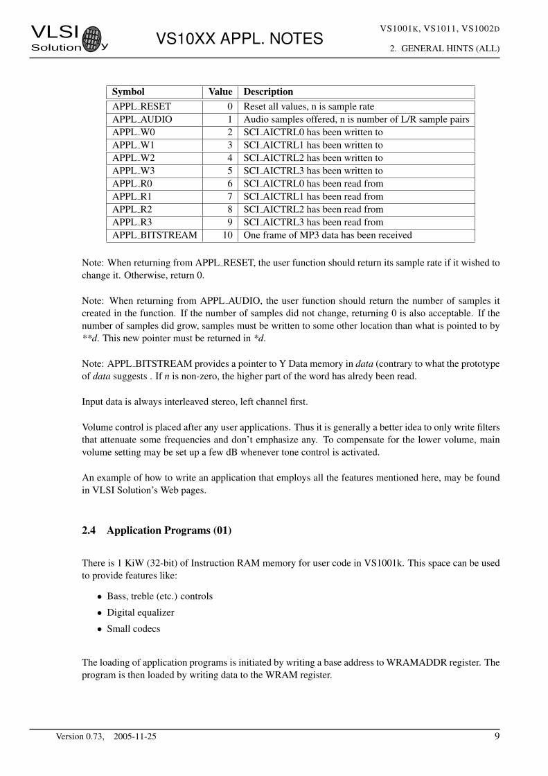
Symbol Value DescriptionAPPL RESET 0 Reset all values, n is sample rateAPPL AUDIO 1 Audio samples offered, n is number of L/R sample pairsAPPL W0 2 SCI AICTRL0 has been written toAPPL W1 3 SCI AICTRL1 has been written toAPPL W2 4 SCI AICTRL2 has been written toAPPL W3 5 SCI AICTRL3 has been written toAPPL R0 6 SCI AICTRL0 has been read fromAPPL R1 7 SCI AICTRL1 has been read fromAPPL R2 8 SCI AICTRL2 has been read fromAPPL R3 9 SCI AICTRL3 has been read fromAPPL BITSTREAM 10 One frame of MP3 data has been received
Note: When returning from APPL RESET, the user function should return its sample rate if it wished tochange it. Otherwise, return 0.
Note: When returning from APPL AUDIO, the user function should return the number of samples itcreated in the function. If the number of samples did not change, returning 0 is also acceptable. If thenumber of samples did grow, samples must be written to some other location than what is pointed to by**d. This new pointer must be returned in *d.
Note: APPL BITSTREAM provides a pointer to Y Data memory in data (contrary to what the prototypeof data suggests . If n is non-zero, the higher part of the word has alredy been read.
Input data is always interleaved stereo, left channel first.
Volume control is placed after any user applications. Thus it is generally a better idea to only write filtersthat attenuate some frequencies and don’t emphasize any. To compensate for the lower volume, mainvolume setting may be set up a few dB whenever tone control is activated.
An example of how to write an application that employs all the features mentioned here, may be foundin VLSI Solution’s Web pages.
2.4 Application Programs (01)
There is 1 KiW (32-bit) of Instruction RAM memory for user code in VS1001k. This space can be usedto provide features like:
• Bass, treble (etc.) controls
• Digital equalizer
• Small codecs
The loading of application programs is initiated by writing a base address to WRAMADDR register. Theprogram is then loaded by writing data to the WRAM register.
Version 0.73, 2005-11-25 9
VLSISolution y VS10XX APPL. NOTES
VS1001K, VS1011, VS1002D
2. GENERAL HINTS (ALL)
Any programs have to be reloaded every time the chip loses its power supply. The application addressdoes not have to be set every time after the system software has been reset.
The C prototype for the application function is as follows:
void (*applAddr) (register s int16 i0 *data, register s int16 a0 chan, register s int16 a1 nSampl);
If chan is either 1 or 2, the user may do in-place filtering of data. chan is the number of channels, andnSampl is the total number of samples to be handled. With a stereo signal, the left and right channelsamples are interleaved. The program may trust in that nSampl is always divisible by 4.
If chan is 3, the volume has been set using SCI volume setting. In this case the volume is set automati-cally, but software is still provided with some data of the new volume setting: nSampl contains the userselected volume setting, and d points to the left volume multiplier register. The right volume multiplieris in d + 1. The volume value is unsigned, and 32768 corresponds to a gain of 1.0 (e.g. 16384− > 0.5).
If chan is 4..5, AICTRL[chan-4] has been called, and the user given value is in nSampl.
Volume control is placed after any user applications. Thus it is generally a better idea to only write filtersthat attenuate some frequencies and don’t emphasize any. To compensate for the lower volume, mainvolume setting may be set up a few dB whenever tone control is activated.
An example of how to write an application that employs all the features mentioned here, may be foundin separate application notes, available on VLSI Solution’s Web pages.
Version 0.73, 2005-11-25 10
VLSISolution y VS10XX APPL. NOTES
VS1001K, VS1011, VS1002D
3. CLOCK SPEEDS (ALL)
3 Clock Speeds (all)
3.1 General (all)
The VS10XX chips operate typically on a single 24.576 MHz fundamental frequency master clock. Thisclock can be generated by external circuitry (connected to pin XTALI) or by the internal clock chrystalinterface (pins XTALI and XTALO). This clock is sufficient to support a high quality audio output foralmost all the standard sample rates and bit-rates (see Chapter 3). However, using DSP effects mayrequire more processing power.
Note: All VS10XX family processors can not run at all clock speeds mentioned in this chapter. Checkindividual datasheets for details.
Note: Oscillators above 24.576 MHz are usually so-called 3rd harmonic clocks, which have a funda-mental frequency of 1/3 of the nominal clock frequency. With such an oscillator, VS10XX would berunning at the base frequency, if working at all. Thus, for instance, if you run VS10XX with a 32 MHz3rd harmonic clock, you usually end up running the chip at 32 MHz / 3 = 10.67 MHz.
Using another clock speed than the default 24.576 MHz changes the behaviour of VS10XX in manyways. The effects of different clock rates are discussed in this chapter.
3.2 Maximum Sample Rate (all)
With a 24.576 MHz or higher clock, the maximum sample rate is 48000 Hz. For a lower clock, 48000 ∗ClockInMHz/24.576 rounded downwards to the next allowed MP3 sample rate tells the maximumavailable sample rate. Thus, with a 15 MHz clock it is possible to decode playback at 29297− > 24000Hz.
To put it another way: if VS10XX is run with a 26 MHz clock, the maximum playback frequency wouldbe 50781 Hz, and all MPEG audio files can be played correctly. However, with a 24 MHz clock themaximum playback rate is only 46875 Hz. In this case, all sample rates upto 44100 Hz can be playedwithout problems, but 48000 Hz is played at 46875 Hz, or in other words with a 2.5% speed error.
3.3 Maximum Amount of DSP Effects (all)
With a 24.576 MHz clock there is some 7 MHz free processor time (minimum) for a 128 kbit/s 44.1 kHzbitstream. However, with 256 kbit/s at 48 kHz there is no constant free time: although the average loadis at approx. 22.5 MHz, peaks require somewhat more processing power (see Chapter 3.4).
If it is desired to be able to play higher-width bitstreams at the same time with special effects or tonecontrols, a higher clock rate is required. Notice, that the internal tone controller that can be activatedwith the SM BASS bit of SCI register MODE, requires 1.59 MHz additional processing power.
If a user wants to have a lower clock but still have DSP special effects, it may be a good idea to researchthe bitstream through the AUDATA register. If the bitstream width and sample rates seem to be too high,turn DSP effects off using the AIADDR register; otherwise turn them on.
Version 0.73, 2005-11-25 11
VLSISolution y VS10XX APPL. NOTES
VS1001K, VS1011, VS1002D
3. CLOCK SPEEDS (ALL)
3.4 Maximum Decodable Bitstream (all)
The maximum bitstream that can be correctly decoded depends on the internal clock frequency CLKI.The following subsections describe what kinds of sample rates and bit rates can be decoded with differentclock rates.
If the user tries to play back a stream that has a too high sample rate, it will be played with the highestsample rate available as described in Chapter 3.2. if a user tries to play a 32 kHz MP3 file with a 12.288MHz clock, it will be played back at 24 kHz, i.e. 2/3 of the correct speed.
If the user tries to play back a stream that has too high a bitrate, it will be played back too slowly andwith some gaps in the sound. If the difference is very small, the gaps may be unnoticeable. Example:if one tries to play back a constant bitrate file with 256 kbit/s with a 24.576 MHz clock, the file will atsome points be played back a bit slowly. However, in many cases, this cannot be noticed, because decodeproblems occur usually at transients where the ear doesn’t very easy hear small glitches.
3.4.1 CLKI = 12.288 MHz (all)
Sample rates upto 24 kHz may be decoded from bitstreams upto 96 kbit/s.
3.4.2 CLKI = 22.580 MHz (all)
Sample rates upto 44.1 kHz may be decoded from bitstreams upto 160 kbit/s. Normally, variable bitratefiles with upto 256 kbit/s peaks may be played without glitches.
3.4.3 CLKI = 24.576 MHz (all)
From this frequency on, all sample rates (i.e. upto 48 kHz) may be decoded from bitstreams upto 192kbit/s. 256 kbit/s bitstreams usually have so little glitches that they cannot be heard. Normally, variablebitrate files with upto 256 or even 320 kbit/s peaks may be played without any glitches.
3.4.4 CLKI = 26.000 MHz (all)
Bitstreams upto 256 kbit/s can be decoded. Normally, variable bitrate files with upto 320 kbit/s peaksmay be played without any glitches.
3.4.5 CLKI = 28.000 MHz (all)
Bitstreams upto 320 kbit/s can be decoded, with both constant and variable bitrates. Note that allVS10XX products are not qualified for this operational frequency.
Version 0.73, 2005-11-25 12
VLSISolution y VS10XX APPL. NOTES
VS1001K, VS1011, VS1002D
4. QUICK STARTUP (ALL)
4 Quick Startup (all)
4.1 Overview (all)
This chapter is meant to be read after the first device using VS10XX has been built. In this chapter thefirst steps to get VS10XX up and running are discussed. In addition to this chapter, also Chapter 7 isuseful for the first steps.
These tests have been meant to be run one at a time, and the next test is to be done only after the previousone has been passed.
4.2 Seeing If Analog Works (all)
(This test may be omitted without affecting the later ones.)
Connect all DVDD pins, XRESET, all AVDD pins and TEST0 to the voltage specified in the chipsdatasheet. Connect DGND and all AGND pins to ground.
Measure voltage of RCAP, it should be about 1.3 V. If it is 0 V or the same as operating voltage, there isa problem with VS10XX’s analog parts.
4.3 Seeing If Firmware Wakes Up (all)
When VS10XX is taken out of hardware reset (xRESET is turned to 1), DREQ should turn to 0 afterapprox. 4096 clock cycles, if it hasn’t been down all the time. After yet another 6000 clock cycles,DREQ should turn to 1. If DREQ doesn’t change its mode as described, the firmware is not functioningproperly.
4.4 Writing to SCI (11, 02)
The first test that does anything useful is to try to write to the SCI bus. A good test is to try to run thesoftware reset and see if the chip’s DREQ goes down and up again as explained in Chapter 4.3.
The following algorithm can be used to test SCI this way:
• Activate xCS by setting it to 0.• Reset the firmware by writing four SCI bytes: 0x2, 0x0, 0x0, 0x4• Finish SCI cycle by setting xCS to 1.• See if you can catch DREQ quickly flying down and up again.• Wait for example 100 ms.
Version 0.73, 2005-11-25 13
VLSISolution y VS10XX APPL. NOTES
VS1001K, VS1011, VS1002D
4. QUICK STARTUP (ALL)
4.5 Writing to SCI (01)
The first test that does anything useful is to try to write to the SCI bus. A good test is to try to switch thevolume setting from powersave mode to full volume. This will cause slight snapping sounds, which canbe checked with the earphones.
The following algorithm can be used to test SCI this way:
• Activate xCS by setting it to 0.• Set full volume by writing four SCI bytes: 0x2, 0xB, 0x0, 0x0• Finish SCI cycle setting xCS to 1.• Wait for example 500 ms.• Activate xCS by setting it to 0.• Set analog powerdown by writing four SCI bytes: 0x2, 0xB, 0xFF, 0xFF• Wait for example 500 ms.• Finish SCI cycle setting xCS to 1.• Repeat these steps indefinitely.
4.6 Reading from SCI (all)
Now that we know writing to SCI works, we can try reading from it. Write some recognizable pattern tothe volume register as described in 4.5, like 0xA2F5 (this is a good pattern, because it effectively testsboth the MSB and LSB). Then, do as follows:
• Activate xCS by setting it to 0.• Read the volume register as described in 7.3.3.• Check, if the result is 0xA2F5.• Finish SCI cycle setting xCS to 1.
4.7 Writing to SDI (01; 11’s and 02’s compatibility mode)
Writing to the actual MP3 data SDI bus is most easily tested with the special VS10XX test header, likethe sine test.
• If using VS1011 or VS1002d, allow tests by writing to SCI: 0x2, 0x0, 0x8, 0x20.• Activate the sine test by writing the following eight bytes to SDI: 0x53 0xEF 0x6E 0x30, 0, 0, 0,
0. Remember to take care of BSYNC properly.• Wait for example 500 ms.• Deactivate the sine test by writing to SDI: 0x45 0x78 0x69 0x74.• Wait for example 500 ms.• Repeat these steps indefinitely.
Version 0.73, 2005-11-25 14
VLSISolution y VS10XX APPL. NOTES
VS1001K, VS1011, VS1002D
4. QUICK STARTUP (ALL)
If you can hear a half-second beep every second, you have properly entered and exited the sine test mode.
Note: Unless you atteanuate volume at least -20 dB from full volume, the sine tone will be very loud. Itis thus not recommended to keep your headphones on while conducting this test.
4.8 Writing to SDI (11’s and 02’s new mode)
Writing to the actual MP3 data SDI bus is most easily tested with the special VS10XX test header, likethe sine test.
Before activating the test, check whether you want just to use VS10XX’s New Mode, or if you also wantto use Shared Mode. With New Mode, you need 5 pins for a connection, with New Mode + Shared Modeyou need only 4.
Steps before the actual test in New Mode (not shared):• Activate xCS by setting it to 0.• Set New Mode by writing four SCI bytes: 0x2, 0x0, 0x8, 0x20• Finish SCI cycle by setting xCS to 1.• Activate xDCS (which now replaces BSYNC) by setting it to 0.
Steps before the actual test in New Mode + Shared Mode:• Activate xCS by setting it to 0.• Set New Mode by writing four SCI bytes: 0x2, 0x0, 0xc, 0x20• Finish SCI cycle and activate SDI by setting xCS to 1.
After one of the previous steps, do as follows:• Activate the sine test by writing the following eight bytes to SDI: 0x53 0xEF 0x6E 0x44, 0, 0, 0,
0.• Wait for example 500 ms.• Deactivate the sine test by writing to SDI: 0x45 0x78 0x69 0x74.• Wait for example 500 ms.• Repeat these steps indefinitely.
If you can hear a half-second beep every second, you have properly entered and exited the sine test mode.
Note: Unless you atteanuate volume at least -20 dB from full volume, the sine tone will be very loud. Itis thus not recommended to keep your headphones on while conducting this test.
Version 0.73, 2005-11-25 15
VLSISolution y VS10XX APPL. NOTES
VS1001K, VS1011, VS1002D
5. HOW TO PLAY A SONG (11, 02)
5 How to Play a Song (11, 02)
This chapter describes how to properly boot up VS1011/VS1002d and play songs with them.
1. Power-up VS10xx as explained in Chapter 8.
2. Deassert xRESET.
3. Wait until DREQ goes to 1.
4. Set SCI MODE register bits, including correct values for SM SDINEW and SM SDISHARED.
5. If your clock rate is not 24.576 MHz, set SCI CLOCKF.
6. If you use the clock doubler and you want your change to SCI CLOCKF to take immediate effect,write a sample rate to SCI AUDATA. 10000 clock cycles after this VS10xx is running at clock-doubled speed and you may use a higher SPI speed if you want to (Chapter 12).
7. Set volume register SCI VOL.
8. If you want to set the bass booster, set SCI BASS.
9. If you have user code to be loaded to VS10xx’s RAM memory, load it and activate it usingSCI WRAM, SCI WRAMADDR and SCI AIADDR.
10. Start sending the audio file to VS10xx, keeping in mind rules about DREQ.
11. After the song has ended, if you want to make sure no audio is left unplayed, follow the song with2048 zeros to SDI.
12. If you have user code active, deactivate it by writing 0 to AIADDR.
13. Activate the SM RESET bit in SCI MODE.
14. Goto point 3.
Version 0.73, 2005-11-25 16
VLSISolution y VS10XX APPL. NOTES
VS1001K, VS1011, VS1002D
6. SAVING I/O PINS (11, 02)
6 Saving I/O Pins (11, 02)
6.1 Overview (11, 02)
Connecting VS1011/VS1002d to a microcontroller requires from 5 to 9 pins, depending on how they areconnected.
The most pin-consuming way to connect VS1011/VS1002d is to use the old VS1001k compatibilitymode. This mode should not be used for new projects.
6.2 SPI With Other Devices Connected (11, 02)
Mic
roco
ntr
olle
r
SO
SI
SCLK
xCS
SCK
MOSI
MISO
GIO1
GIO2
GIO3
xDCS
DREQ
VS
1011/VS
1002c
SC
LK
xCS
xRST
GIO
5G
IO4
Other SPI slave
MIS
O
MO
SI
xRE
SE
T
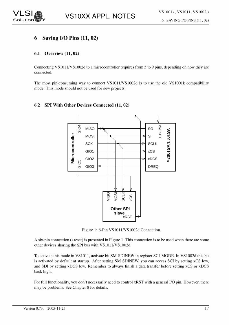
Figure 1: 6-Pin VS1011/VS1002d Connection.
A six-pin connection (+reset) is presented in Figure 1. This connection is to be used when there are someother devices sharing the SPI bus with VS1011/VS1002d.
To activate this mode in VS1011, activate bit SM SDINEW in register SCI MODE. In VS1002d this bitis activated by default at startup. After setting SM SDINEW, you can access SCI by setting xCS low,and SDI by setting xDCS low. Remember to always finish a data transfer before setting xCS or xDCSback high.
For full functionality, you don’t necessarily need to control xRST with a general I/O pin. However, theremay be problems. See Chapter 8 for details.
Version 0.73, 2005-11-25 17
VLSISolution y VS10XX APPL. NOTES
VS1001K, VS1011, VS1002D
6. SAVING I/O PINS (11, 02)
6.3 SPI With VS10XX As the Only Device (11, 02)
Mic
roco
ntr
olle
r
SO
SI
SCLK
xCS
SCK
MOSI
MISO
GIO1
GIO3 DREQ
VS
1011/VS
1002c
GIO
4 xRE
SE
T
xDCS
VCC
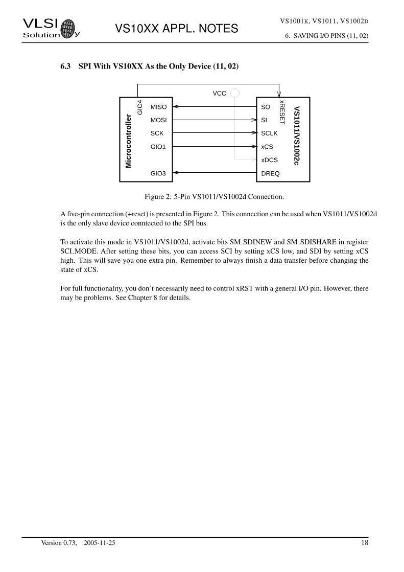
Figure 2: 5-Pin VS1011/VS1002d Connection.
A five-pin connection (+reset) is presented in Figure 2. This connection can be used when VS1011/VS1002dis the only slave device conntected to the SPI bus.
To activate this mode in VS1011/VS1002d, activate bits SM SDINEW and SM SDISHARE in registerSCI MODE. After setting these bits, you can access SCI by setting xCS low, and SDI by setting xCShigh. This will save you one extra pin. Remember to always finish a data transfer before changing thestate of xCS.
For full functionality, you don’t necessarily need to control xRST with a general I/O pin. However, theremay be problems. See Chapter 8 for details.
Version 0.73, 2005-11-25 18
VLSISolution y VS10XX APPL. NOTES
VS1001K, VS1011, VS1002D
7. SAVING I/O PINS (01)
7 Saving I/O Pins (01)
7.1 Overview (01)
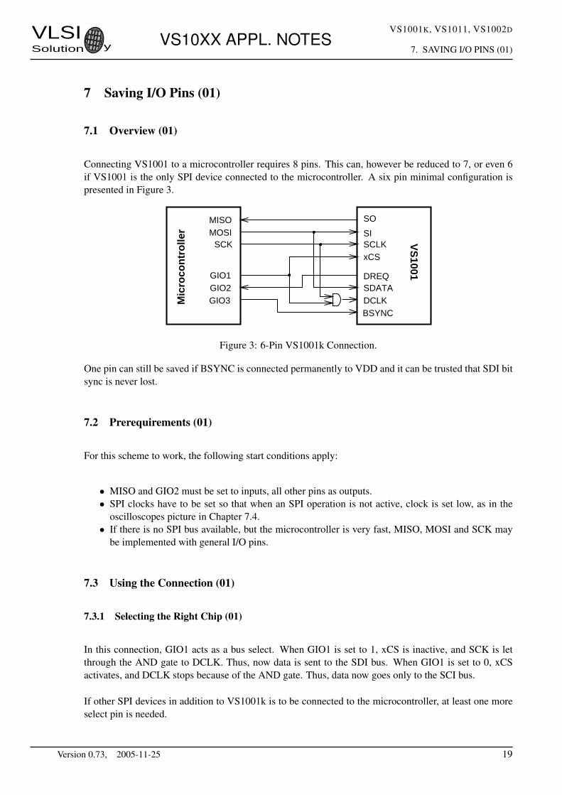
Connecting VS1001 to a microcontroller requires 8 pins. This can, however be reduced to 7, or even 6if VS1001 is the only SPI device connected to the microcontroller. A six pin minimal configuration ispresented in Figure 3.
Mic
roco
ntr
olle
r
VS
1001
SO
SISCLKxCS
DREQSDATADCLKBSYNC
SCKMOSIMISO
GIO1GIO2GIO3
Figure 3: 6-Pin VS1001k Connection.
One pin can still be saved if BSYNC is connected permanently to VDD and it can be trusted that SDI bitsync is never lost.
7.2 Prerequirements (01)
For this scheme to work, the following start conditions apply:
• MISO and GIO2 must be set to inputs, all other pins as outputs.• SPI clocks have to be set so that when an SPI operation is not active, clock is set low, as in the
oscilloscopes picture in Chapter 7.4.• If there is no SPI bus available, but the microcontroller is very fast, MISO, MOSI and SCK may
be implemented with general I/O pins.
7.3 Using the Connection (01)
7.3.1 Selecting the Right Chip (01)
In this connection, GIO1 acts as a bus select. When GIO1 is set to 1, xCS is inactive, and SCK is letthrough the AND gate to DCLK. Thus, now data is sent to the SDI bus. When GIO1 is set to 0, xCSactivates, and DCLK stops because of the AND gate. Thus, data now goes only to the SCI bus.
If other SPI devices in addition to VS1001k is to be connected to the microcontroller, at least one moreselect pin is needed.
Version 0.73, 2005-11-25 19
VLSISolution y VS10XX APPL. NOTES
VS1001K, VS1011, VS1002D
7. SAVING I/O PINS (01)
7.3.2 Sending SCI Data (01)
Let’s say we would like to set the volume to -2 dB for the left channel and to -3.5 dB to the right channel.Thus, we would like to write the number 0x0407 to the VOL register.
• Activate the SCI interface by setting GIO1 to 0• Write the four bytes (0x2, 0xb, 0x4, 0x7) to SCI.• Finish the SCI transaction by setting GIO1 to 1
7.3.3 Receiving SCI Data (01)
Let’s say we would like to read the contents of the VOL register.
• Activate the SCI interface by setting GIO1 to 0• Write two bytes (0x3, 0xb) to SCI.• Write one byte with any contents to SCI. Read the microcontroller’s MISO register, which now
contains 8 MSBs of the result.• Write one byte with any contents to SCI. Read the microcontroller’s MISO register, which now
contains 8 LSBs of the result.• Combine the MSBs and LSBs to form a 16-bit word.• Finish the SCI transaction by setting GIO1 to 1
7.3.4 Sending SDI/MP3 Data (01)
The following algorithm may be used to send a 32-byte or smaller MP3 data chunk to VS1001k:
• Wait until DREQ is 1.• Activate DCLK by setting GIO to 1.• For each byte, do the following:
– Set BSYNC to 1.
– Activate SPI transfer.
– Wait until you know that at least the first bit of data has been sent, and the last bit has notbeen sent. Although VS1001k can survive several too long BSYNCs, it may be a good ideato disable interrupts to make sure the delay always is the same length.
– Set BSYNC to 0.
– Wait for microcontroller’s SPI cycle to finish.
Version 0.73, 2005-11-25 20
VLSISolution y VS10XX APPL. NOTES
VS1001K, VS1011, VS1002D
7. SAVING I/O PINS (01)
7.4 SDI in Oscilloscope Pictures (01)
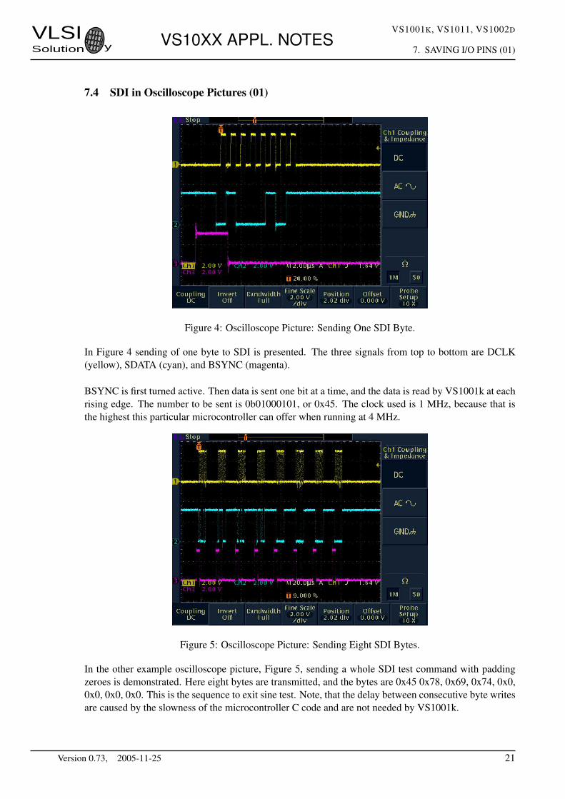
Figure 4: Oscilloscope Picture: Sending One SDI Byte.
In Figure 4 sending of one byte to SDI is presented. The three signals from top to bottom are DCLK(yellow), SDATA (cyan), and BSYNC (magenta).
BSYNC is first turned active. Then data is sent one bit at a time, and the data is read by VS1001k at eachrising edge. The number to be sent is 0b01000101, or 0x45. The clock used is 1 MHz, because that isthe highest this particular microcontroller can offer when running at 4 MHz.
Figure 5: Oscilloscope Picture: Sending Eight SDI Bytes.
In the other example oscilloscope picture, Figure 5, sending a whole SDI test command with paddingzeroes is demonstrated. Here eight bytes are transmitted, and the bytes are 0x45 0x78, 0x69, 0x74, 0x0,0x0, 0x0, 0x0. This is the sequence to exit sine test. Note, that the delay between consecutive byte writesare caused by the slowness of the microcontroller C code and are not needed by VS1001k.
Version 0.73, 2005-11-25 21
VLSISolution y VS10XX APPL. NOTES
VS1001K, VS1011, VS1002D
8. POWERING UP AND DOWN CLEANLY (11, 02)
8 Powering Up and Down Cleanly (11, 02)
Powering up and down a component with analog earphone outputs needs some special consideration ifthe user wants to avoid unwanted transients, which may be heard as clicks on startup. By followingthe instructions of this chapter, the user of VS1011/VS1002d can power up and down their units withtransients of less than 50 mV, which is 20 dB lower than the 400 mV startup transient of VS1001k.
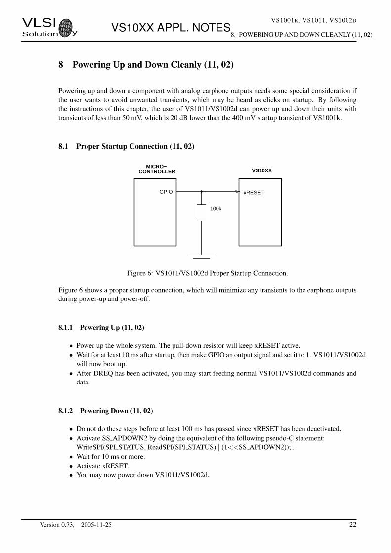
8.1 Proper Startup Connection (11, 02)
GPIO
MICRO−CONTROLLER VS10XX
100k
xRESET
Figure 6: VS1011/VS1002d Proper Startup Connection.
Figure 6 shows a proper startup connection, which will minimize any transients to the earphone outputsduring power-up and power-off.
8.1.1 Powering Up (11, 02)
• Power up the whole system. The pull-down resistor will keep xRESET active.• Wait for at least 10 ms after startup, then make GPIO an output signal and set it to 1. VS1011/VS1002d
will now boot up.• After DREQ has been activated, you may start feeding normal VS1011/VS1002d commands and
data.
8.1.2 Powering Down (11, 02)
• Do not do these steps before at least 100 ms has passed since xRESET has been deactivated.• Activate SS APDOWN2 by doing the equivalent of the following pseudo-C statement:
WriteSPI(SPI STATUS, ReadSPI(SPI STATUS) | (1<<SS APDOWN2)); .• Wait for 10 ms or more.• Activate xRESET.• You may now power down VS1011/VS1002d.
Version 0.73, 2005-11-25 22
VLSISolution y VS10XX APPL. NOTES
VS1001K, VS1011, VS1002D
8. POWERING UP AND DOWN CLEANLY (11, 02)
8.2 Functional Connection (11, 02)
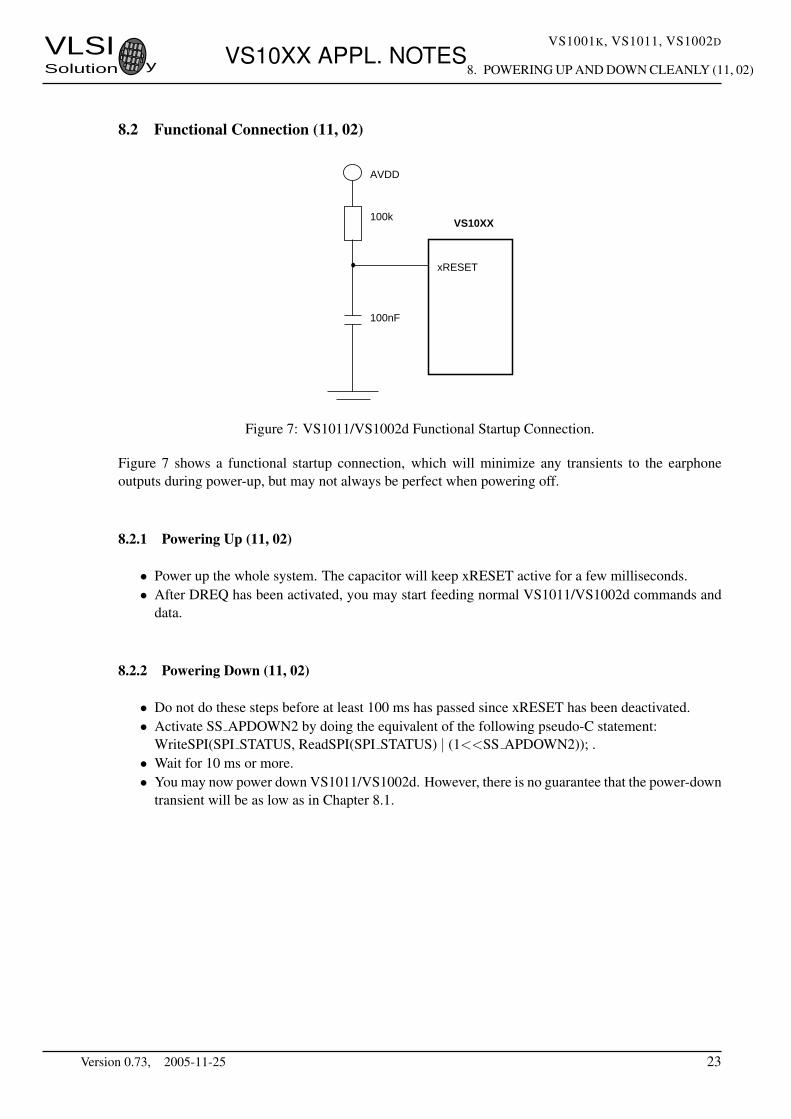
VS10XX
AVDD
100k
100nF
xRESET
Figure 7: VS1011/VS1002d Functional Startup Connection.
Figure 7 shows a functional startup connection, which will minimize any transients to the earphoneoutputs during power-up, but may not always be perfect when powering off.
8.2.1 Powering Up (11, 02)
• Power up the whole system. The capacitor will keep xRESET active for a few milliseconds.• After DREQ has been activated, you may start feeding normal VS1011/VS1002d commands and
data.
8.2.2 Powering Down (11, 02)
• Do not do these steps before at least 100 ms has passed since xRESET has been deactivated.• Activate SS APDOWN2 by doing the equivalent of the following pseudo-C statement:
WriteSPI(SPI STATUS, ReadSPI(SPI STATUS) | (1<<SS APDOWN2)); .• Wait for 10 ms or more.• You may now power down VS1011/VS1002d. However, there is no guarantee that the power-down
transient will be as low as in Chapter 8.1.
Version 0.73, 2005-11-25 23
VLSISolution y VS10XX APPL. NOTES
VS1001K, VS1011, VS1002D
9. DECLICKING VS1001K (01)
9 Declicking VS1001k (01)
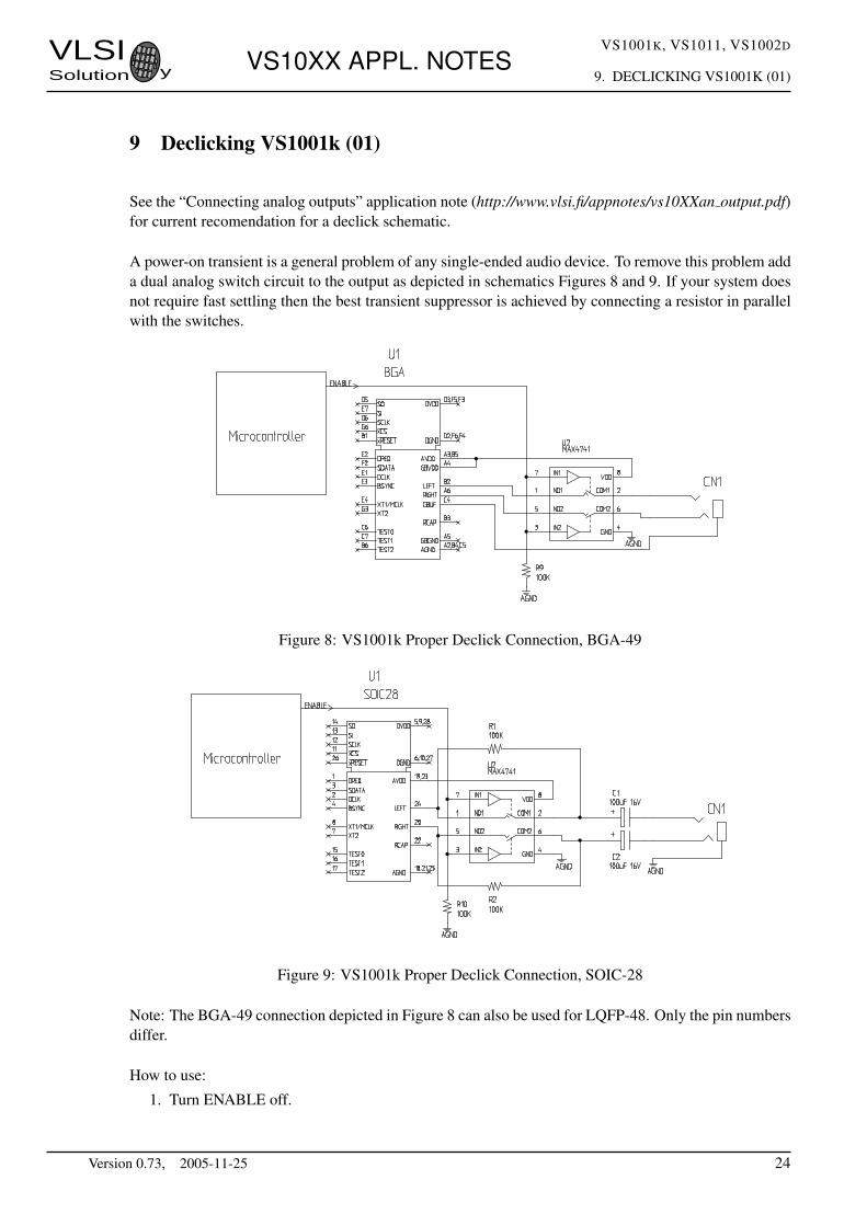
See the “Connecting analog outputs” application note (http://www.vlsi.fi/appnotes/vs10XXan output.pdf)for current recomendation for a declick schematic.
A power-on transient is a general problem of any single-ended audio device. To remove this problem adda dual analog switch circuit to the output as depicted in schematics Figures 8 and 9. If your system doesnot require fast settling then the best transient suppressor is achieved by connecting a resistor in parallelwith the switches.
Figure 8: VS1001k Proper Declick Connection, BGA-49
Figure 9: VS1001k Proper Declick Connection, SOIC-28
Note: The BGA-49 connection depicted in Figure 8 can also be used for LQFP-48. Only the pin numbersdiffer.
How to use:
1. Turn ENABLE off.
Version 0.73, 2005-11-25 24
VLSISolution y VS10XX APPL. NOTES
VS1001K, VS1011, VS1002D
9. DECLICKING VS1001K (01)
2. Reset VS1001 + take it out of reset.
3. Wait for at least 100 ms.
4. Turn ENABLE on.
Note: The minimum wait time 100 ms depends on the 100 nF reference capacitor. If is is larger, you haveto wait longer. The example schematics show a Maxim device. There probable are other and cheaperalternatives available.
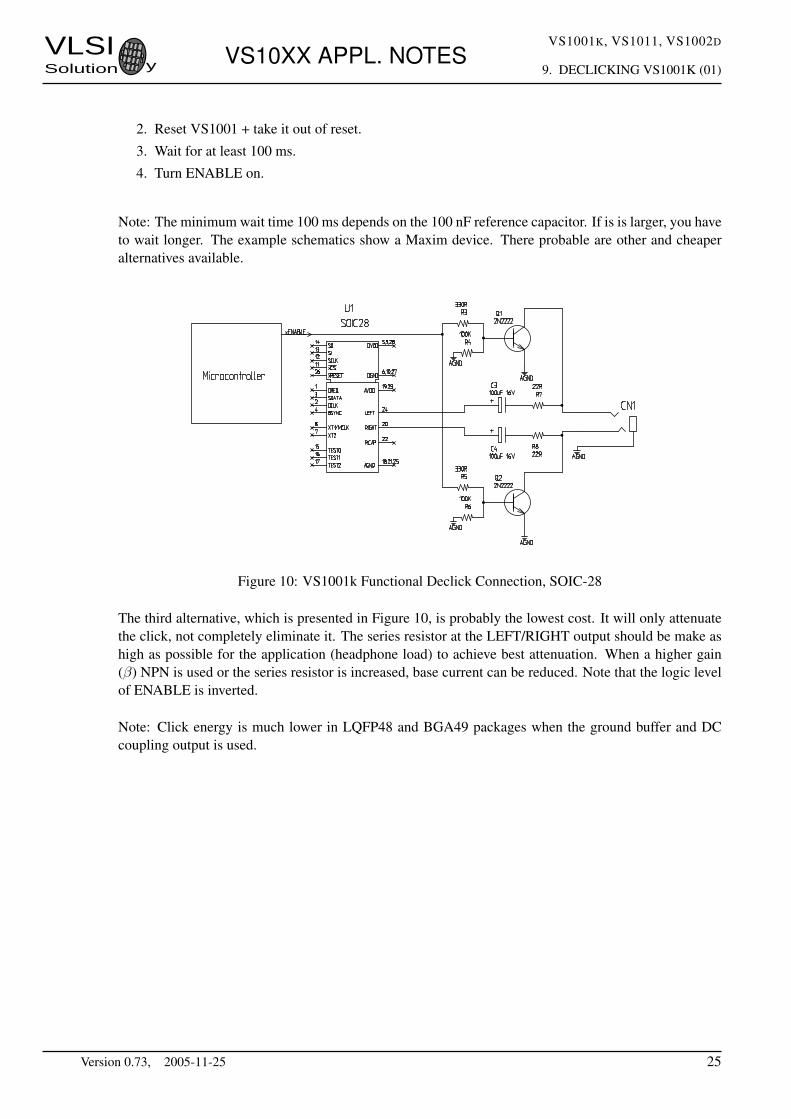
Figure 10: VS1001k Functional Declick Connection, SOIC-28
The third alternative, which is presented in Figure 10, is probably the lowest cost. It will only attenuatethe click, not completely eliminate it. The series resistor at the LEFT/RIGHT output should be make ashigh as possible for the application (headphone load) to achieve best attenuation. When a higher gain(β) NPN is used or the series resistor is increased, base current can be reduced. Note that the logic levelof ENABLE is inverted.
Note: Click energy is much lower in LQFP48 and BGA49 packages when the ground buffer and DCcoupling output is used.
Version 0.73, 2005-11-25 25
VLSISolution y VS10XX APPL. NOTES
VS1001K, VS1011, VS1002D
10. MP3 PLAYER (01)
10 MP3 Player (01)
10.1 Overview (01)
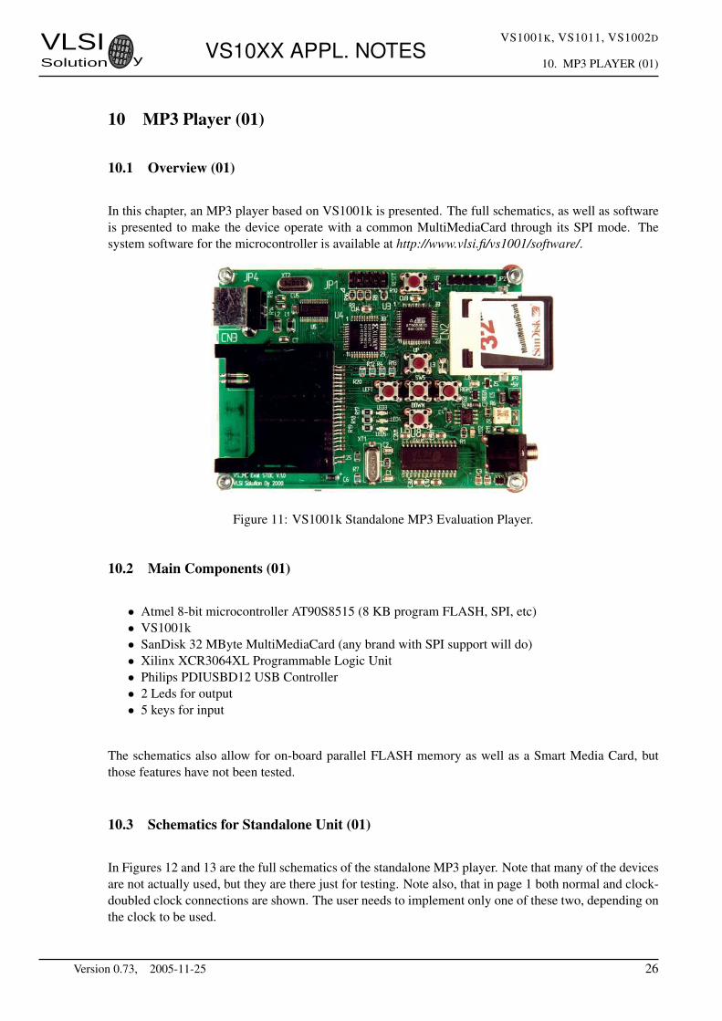
In this chapter, an MP3 player based on VS1001k is presented. The full schematics, as well as softwareis presented to make the device operate with a common MultiMediaCard through its SPI mode. Thesystem software for the microcontroller is available at http://www.vlsi.fi/vs1001/software/.
Figure 11: VS1001k Standalone MP3 Evaluation Player.
10.2 Main Components (01)
• Atmel 8-bit microcontroller AT90S8515 (8 KB program FLASH, SPI, etc)• VS1001k• SanDisk 32 MByte MultiMediaCard (any brand with SPI support will do)• Xilinx XCR3064XL Programmable Logic Unit• Philips PDIUSBD12 USB Controller• 2 Leds for output• 5 keys for input
The schematics also allow for on-board parallel FLASH memory as well as a Smart Media Card, butthose features have not been tested.
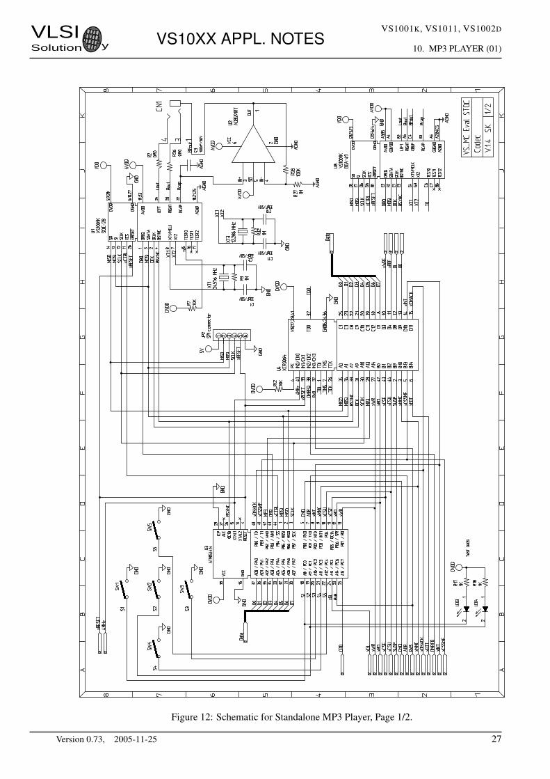
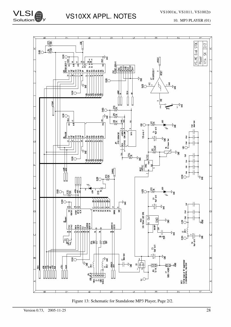
10.3 Schematics for Standalone Unit (01)
In Figures 12 and 13 are the full schematics of the standalone MP3 player. Note that many of the devicesare not actually used, but they are there just for testing. Note also, that in page 1 both normal and clock-doubled clock connections are shown. The user needs to implement only one of these two, depending onthe clock to be used.
Version 0.73, 2005-11-25 26
VLSISolution y VS10XX APPL. NOTES
VS1001K, VS1011, VS1002D
10. MP3 PLAYER (01)
Figure 12: Schematic for Standalone MP3 Player, Page 1/2.
Version 0.73, 2005-11-25 27
VLSISolution y VS10XX APPL. NOTES
VS1001K, VS1011, VS1002D
10. MP3 PLAYER (01)
Figure 13: Schematic for Standalone MP3 Player, Page 2/2.
Version 0.73, 2005-11-25 28
VLSISolution y VS10XX APPL. NOTES
VS1001K, VS1011, VS1002D
10. MP3 PLAYER (01)
10.4 Xilinx Configuration (01)
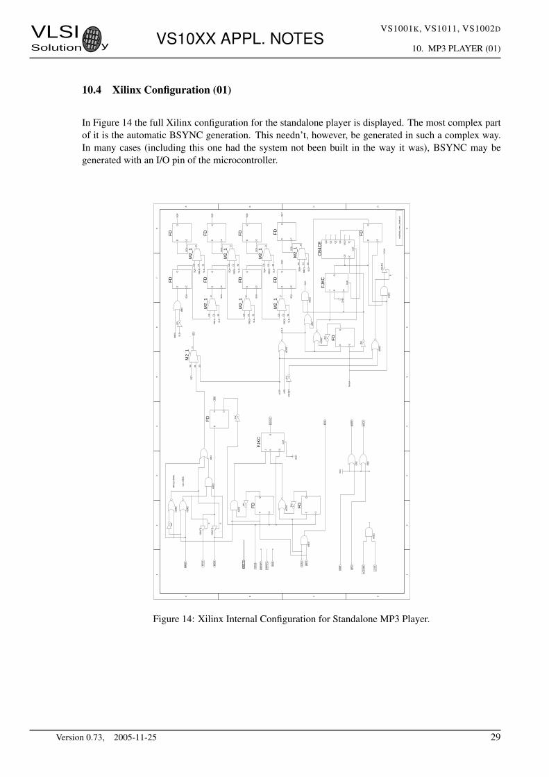
In Figure 14 the full Xilinx configuration for the standalone player is displayed. The most complex partof it is the automatic BSYNC generation. This needn’t, however, be generated in such a complex way.In many cases (including this one had the system not been built in the way it was), BSYNC may begenerated with an I/O pin of the microcontroller.
12
34
56
78
12
34
56
78
A B C D
A B C D
VC
C
M2_
1O
D0
D1
S0
M2_
1O
D0
D1
S0
M2_
1O
D0
D1
S0
M2_
1O
D0
D1
S0
M2_
1O
D0
D1
S0
M2_
1O
D0
D1
S0
M2_
1O
D0
D1
S0
M2_
1O
D0
D1
S0
CLR
C
Q3
Q2
Q1
Q0
TC
CE
CE
O
CB
4CE
OR
3
OR
2
OR
2
OR
2
OR
2
E
OB
UF
E
E
OB
UF
E
E
OB
UF
E
C
CLR
J
QK
FJK
C
C
CLR
J
QK
FJK
C
NO
R2
NO
R2
NO
R2
NO
R2
NO
R2
NO
R2
GN
D
GN
D
INV
INV
INV
INV
INV
INVINV
INV
FD
QD C
FD
QD C
FD
QD C
FD
QD C
FD
QD C
FD
QD C
FD
QD C
FD
QD C
FD
QD C
FD
QD C
FD
QD C
FD
QD C
FD
QD C
AN
D2 A
ND
2
AN
D2
AN
D2
AN
D2
AN
D2
DB
(0)
SQ
4S
LD
xMM
CS
CK
SC
K
SQ
7D
IS
Q3
DB
(4)
MIS
OS
LD
SQ
5M
OS
ID
OD
B(1
)
SLD
SC
KS
CK
SQ
4
DB
(5)
SLD
DB
(0-7
)
SQ
6D
B(2
)
SLD
MH
z4S
CK
SC
K
xRE
SE
T
SQ
5D
MR
EQ
DB
(6)
BS
YN
CR
xBS
LD
xCS
FS
LDS
Q3
SQ
7xR
DD
B(3
)
xRE
SE
TS
LDS
CK
SC
K
SQ
6S
CLK
DB
(7)
SC
KM
P3
SLD
DC
K
xWR
MH
z4xR
DxW
RF
xCS
SM
FxR
DF
xCS
F
SC
LK
vain
xM
MC
MP
3 ja
xM
MC
mp3
stda
_mm
c_dm
a.sc
h
Figure 14: Xilinx Internal Configuration for Standalone MP3 Player.
Version 0.73, 2005-11-25 29
VLSISolution y VS10XX APPL. NOTES
VS1001K, VS1011, VS1002D
11. ESD PROTECTION (ALL)
11 ESD Protection (all)
VS10XX can withstand a maximum ESD charge of 2 kV to its analog outputs (RIGHT, LEFT, GBUF).This is a fundamental limitation of CMOS technology and cannot be helped without external protectioncircuitry. External protection is needed if VS10XX’s analog outputs are to be connected to externalconnectors that may give stronger-than-normal electrical shocks. An example would be earphone plugs,where 15 kV ESD resistance may be required.
See the “Connecting analog outputs” application note (http://www.vlsi.fi/appnotes/vs10XXan output.pdf)for detailed info.
12 Highest SPI Speed (11, 02)
If VS1011 or VS1002d is used without a clock doubler, the maximum SPI speed is 1/6 of the internalclock speed CLKI, which is also the input clock frequency XTALI. If, for instance, the nominal 24.576MHz clock is used, the maximum SPI speed is 24.576MHz
6 , which is slightly over 4 MHz.
However, if a low-frequency external clock is used, and the clock-doubler is to be activated, two initialregister writes must be done to get the clock-doubler activated. Before that the maximum clock speed isXTALI
6 , which with a nominal 12.288 MHz clock is slightly over 2 MHz.
The following register write example is assuming a 12.288 MHz external clock:
1. After a software or hardware reset, first set your SPI clock speed to 2 MHz or lower.
2. Wait until DREQ is active.
3. Write the correct value 0x9800 to SCI CLOCKF (as usual).
4. Set a sample rate to SCI AUDATA, for instance 0x1f40 for 8000 Hz
5. After waiting for at least 11000 clock cycles, you may set your microcontroller SPI clock to upto4 MHz and proceed sending your SCI and SDI data at the higher speed.
13 Highest SPI Speed (01)
If VS1001 is used without a clock doubler, maximum SPI speed is a very simple issue: it is 1/4 of theinput clock frequency XTALI, which is also the internal clock speed CLKI. If, for instance, the nominal24.576 MHz clock is used, the maximum SPI speed is 24.576 MHz / 4, which is slightly over 6 MHz.
However, if a low-frequency external clock is used, and the clock-doubler is activated, there are someissues of the current firmware to be known. Unfortunately, the new clock setting won’t be activatedbefore the first frame of MP3 data has been decoded and VS10XX starts playback. Thus, until the firstframe is decoded, if you are using a 12.288 MHz external clock, the maximum SPI clock is 24.576MHz
4 ,,which is slightly over 3 MHz.
Version 0.73, 2005-11-25 30
VLSISolution y VS10XX APPL. NOTES
VS1001K, VS1011, VS1002D
13. HIGHEST SPI SPEED (01)
For applications that would like to have SPI running well over 3 MHz with the clock-doubler activated,waiting for such a badly specified event as “the first MP3 block to be decoded” is clearly a nuisance. Aworkaround for VS1001 to this is described below.
The following example is assuming a 12.288 MHz external clock:
1. After a software or hardware reset, first set your clock speed to 3 MHz or lower.
2. Write the correct value 0x9800 to SCI register CLOCKF (as usual).
3. Force the clock-doubler on by writing 0x8008 to SCI register INT FCTLH. Don’t touch this reg-ister after this, as it will be later set automatically to a more suitable value! (Note: the datasheetstates that you should never write to this register. This is, however, an exception.)
4. Now you may set your microcontroller SPI clock to upto 6 MHz and proceed sending your songand control data to SDI and SCI as usual.
Version 0.73, 2005-11-25 31
VLSISolution y VS10XX APPL. NOTES
VS1001K, VS1011, VS1002D
14. ADPCM RECORDING (02, 03 ,33)
14 ADPCM Recording (02, 03 ,33)
14.1 Introduction
4-bit ADPCM recording gives a compression ratio of 4:1 compared to linear, 16-bit audio. This makes itpossible to record commercial quality sound (8 kHz) at 32 kbit/s.
The ADPCM implementation in VS1002d offers a slightly enhanced version of basic ADPCM, calledIMA ADPCM, which makes it possible to random-seek in a file with only a 1.3% penalty to the bit-rate(32.44 kbit/s for 8 kHz). VS1003 and VS1033 offer IMA ADCM by default.
In this chapter it is told how to create RIFF/WAV IMA ADPCM format. This is a widely supportedADPCM format and many PC audio playback programs can play it.
For detailed info on VS1003 and VS1033 recording see the appropriate datasheets at:http://www.vlsi.fi/download/download.shtml
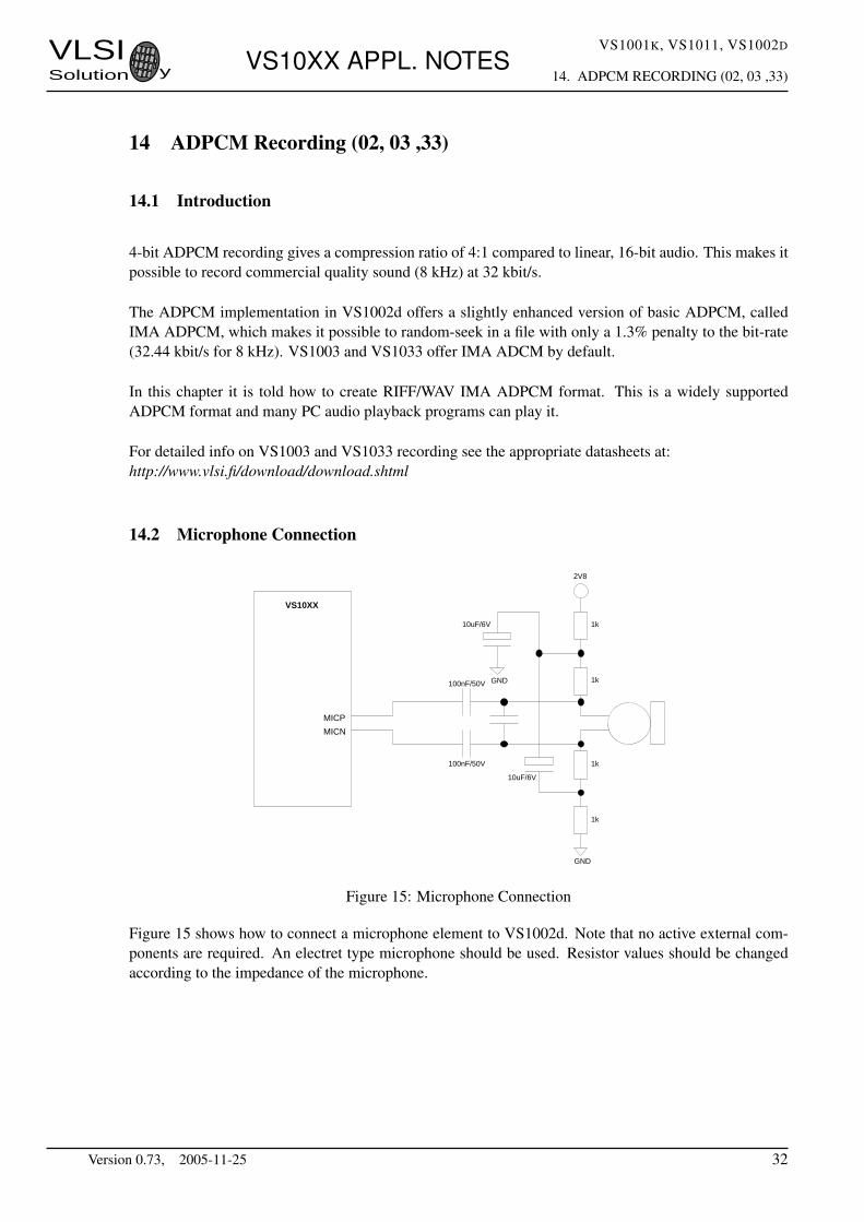
14.2 Microphone Connection
MICP
MICN
1k
1k
1k
1k
10uF/6V
10uF/6V
GND
GND
2V8
100nF/50V
100nF/50V
VS10XX
Figure 15: Microphone Connection
Figure 15 shows how to connect a microphone element to VS1002d. Note that no active external com-ponents are required. An electret type microphone should be used. Resistor values should be changedaccording to the impedance of the microphone.
Version 0.73, 2005-11-25 32
VLSISolution y VS10XX APPL. NOTES
VS1001K, VS1011, VS1002D
14. ADPCM RECORDING (02, 03 ,33)
14.3 Activating ADPCM mode (02)
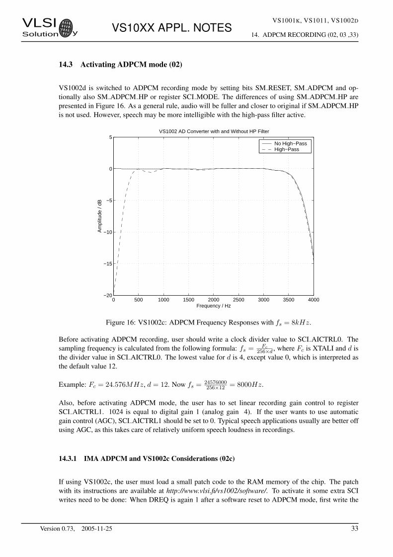
VS1002d is switched to ADPCM recording mode by setting bits SM RESET, SM ADPCM and op-tionally also SM ADPCM HP or register SCI MODE. The differences of using SM ADPCM HP arepresented in Figure 16. As a general rule, audio will be fuller and closer to original if SM ADPCM HPis not used. However, speech may be more intelligible with the high-pass filter active.
0 500 1000 1500 2000 2500 3000 3500 4000−20
−15
−10
−5
0
5VS1002 AD Converter with and Without HP Filter
Frequency / Hz
Am
plitu
de /
dB
No High−PassHigh−Pass
Figure 16: VS1002c: ADPCM Frequency Responses with fs = 8kHz.
Before activating ADPCM recording, user should write a clock divider value to SCI AICTRL0. Thesampling frequency is calculated from the following formula: fs = Fc
256×d , where Fc is XTALI and d isthe divider value in SCI AICTRL0. The lowest value for d is 4, except value 0, which is interpreted asthe default value 12.
Example: Fc = 24.576MHz, d = 12. Now fs = 24576000256×12 = 8000Hz.
Also, before activating ADPCM mode, the user has to set linear recording gain control to registerSCI AICTRL1. 1024 is equal to digital gain 1 (analog gain 4). If the user wants to use automaticgain control (AGC), SCI AICTRL1 should be set to 0. Typical speech applications usually are better offusing AGC, as this takes care of relatively uniform speech loudness in recordings.
14.3.1 IMA ADPCM and VS1002c Considerations (02c)
If using VS1002c, the user must load a small patch code to the RAM memory of the chip. The patchwith its instructions are available at http://www.vlsi.fi/vs1002/software/. To activate it some extra SCIwrites need to be done: When DREQ is again 1 after a software reset to ADPCM mode, first write the
Version 0.73, 2005-11-25 33
VLSISolution y VS10XX APPL. NOTES
VS1001K, VS1011, VS1002D
14. ADPCM RECORDING (02, 03 ,33)
correct clock frequency to SCI CLOCKF (e.g. 0x3000 for 24.576 MHz clock). Then write the fs thatwas calculated earlier to SCI AUDATA (e.g. 8000).
Example: Assume you want to record ADPCM data at 8 kHz with a 12.288 MHz clock and with auto-matic gain control, using new shared mode SCI. To do this, you should:
1. Write 0xC to SCI AICTRL0 (to set sampling rate to 8 kHz)
2. Write 0 to SCI AICTRL1 (to set automatic gain control)
3. Write 0x1C04 to SCI MODE (to software reset and activate ADPCM recording (check that NEW-MODE and other bits are as you want them to be)).
4. Wait 1 ms or until DREQ is 1 after the software reset.
5. Write 0x9800 ro SCI CLOCKF (to set 2 x 12.288 MHz clock)
6. Write 0x1F40 to SCI AUDATA (to set the 8 kHz sample rate)
7. Wait at least 100 µs.
8. If all steps this far have worked, you should be hearing audio loopback from the earphones.
9. Load the ADPCM patch code load ima.cmd to VS1001k’s RAM memory.
10. Issue the following three SCI writes to activate the code:
(a) Write 0x8021 to SCI WRAMADDR
(b) Write 0x2a01 to SCI WRAM
(c) Write 0x000e to SCI WRAM
11. Start reading IMA ADPCM data as described in Chapter 14.4. Remember that a proper IMAADPCM file must also have an IMA ADPCM header.
NOTE! If your external clock is between 12. . . 13 or 24. . . 26 MHz, it is better to let VS1002c believefor ADPCM recording that its clock is 12.288 or 24.576 MHz, respectively. Thus, if you have a 12 MHzclock running with a clock-doubler, don’t write 0x9770 to SCI CLOCKF, but write 0x9800 instead.Also, although fs with divider 12 is really 7812.5 Hz, tell VS1002c that it is 8000 Hz.
14.3.2 IMA ADPCM and VS1002d Considerations (02d)
If using VS1002d, the user may choose to load a patch code to the RAM memory of the chip to increasequality of ADPCM encoding. The patch and instructions reside at http://www.vlsi.fi/vs1002/software/.To activate it do as follows:
Example: Assume you want to record ADPCM data at 8 kHz with a 12.288 MHz clock and with auto-matic gain control, using new shared mode SCI. To do this, you should:
1. Write 0xC04 to SCI MODE (to reset VS1002d on new shared mode).
Version 0.73, 2005-11-25 34
VLSISolution y VS10XX APPL. NOTES
VS1001K, VS1011, VS1002D
14. ADPCM RECORDING (02, 03 ,33)
2. Load the ADPCM patch code load ima.cmd to VS1001k’s RAM memory.
3. Write 0xC to SCI AICTRL0 (to set sampling rate to 8 kHz).
4. Write 0 to SCI AICTRL1 (to set automatic gain control).
5. Write 0x9800 ro SCI CLOCKF (to set 2 x 12.288 MHz clock).
6. Write 0x30 to SCI AIADDR to activate ADPCM recording patch.
7. If all steps this far have worked, you should be hearing audio loopback from the earphones.
8. Start reading IMA ADPCM data as described in Chapter 14.4. Remember that a proper IMAADPCM file must also have an IMA ADPCM header.
14.4 Reading ADPCM Data (02)
After ADPCM recording has been activated, registers SCI HDAT0 and SCI HDAT1 have new functions.
Old Function New FunctionSCI HDAT0 SCI DATASCI HDAT1 SCI BUF FILL
The ADPCM sample buffer is 1024 16-bit words, or in other words, 2 KiB long. If the buffer is overfilled,it will clear automatically. The fill rate of the buffer can be read from SCI BUF FILL, which tells thebuffer fill ratio in 16-bit words. If SCI BUF FILL is greater than 0, you can read SCI BUF FILL 16-bitwords from SCI DATA.
Note: if SCI BUF FILL ≥ 896, it may be better to wait for the buffer to overflow and clear beforereading samples. That way you may avoid buffer aliasing.
Data is provided in 128-word blocks. If you wish to stop reading data and possibly continue later, pleasestop at a block border. This way you will get valid samples immediately when you continue reading.
14.5 Storing ADPCM Data (02)
ADPCM data is provided in IMA ADPCM format, which is a common and widely supported ADPCMformat in the PC world. The good thing about this format is that it is block-oriented, which makes itpossible to do seeks in a file.
16-bit ADPCM values that are read from SCI DATA are to be interpreted as big-endian values. In otherwords, the first 8 bits of data received from the SPI bus are bits 15:8, and should also be written as thefirst byte to a file. Note that this is contrary to the default operation of some 16-bit microcontrollers, andyou may have to take extra care to do this right.
A way to see if you have written the file in the right way is to check bytes 2 and 3 (the first byte countsas byte 0) of each 256-byte block. Byte 3 should always be zero.
Version 0.73, 2005-11-25 35
VLSISolution y VS10XX APPL. NOTES
VS1001K, VS1011, VS1002D
14. ADPCM RECORDING (02, 03 ,33)
14.6 Adding a RIFF Header (02)
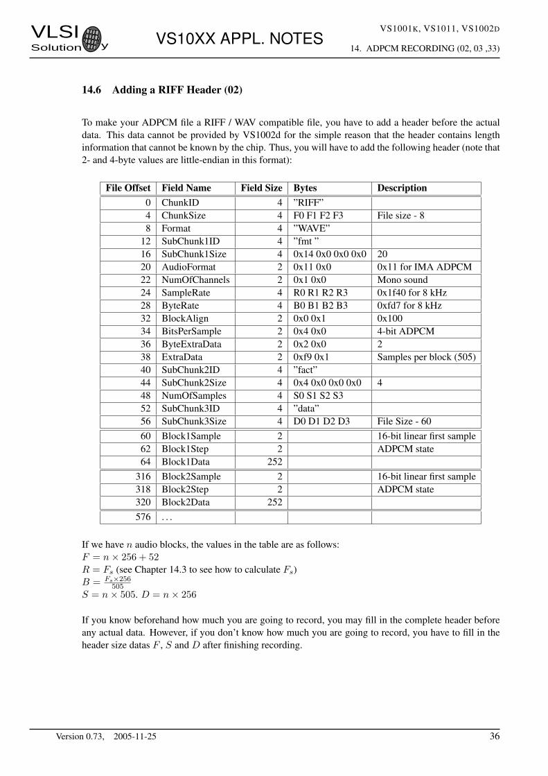
To make your ADPCM file a RIFF / WAV compatible file, you have to add a header before the actualdata. This data cannot be provided by VS1002d for the simple reason that the header contains lengthinformation that cannot be known by the chip. Thus, you will have to add the following header (note that2- and 4-byte values are little-endian in this format):
File Offset Field Name Field Size Bytes Description0 ChunkID 4 ”RIFF”4 ChunkSize 4 F0 F1 F2 F3 File size - 88 Format 4 ”WAVE”
12 SubChunk1ID 4 ”fmt ”16 SubChunk1Size 4 0x14 0x0 0x0 0x0 2020 AudioFormat 2 0x11 0x0 0x11 for IMA ADPCM22 NumOfChannels 2 0x1 0x0 Mono sound24 SampleRate 4 R0 R1 R2 R3 0x1f40 for 8 kHz28 ByteRate 4 B0 B1 B2 B3 0xfd7 for 8 kHz32 BlockAlign 2 0x0 0x1 0x10034 BitsPerSample 2 0x4 0x0 4-bit ADPCM36 ByteExtraData 2 0x2 0x0 238 ExtraData 2 0xf9 0x1 Samples per block (505)40 SubChunk2ID 4 ”fact”44 SubChunk2Size 4 0x4 0x0 0x0 0x0 448 NumOfSamples 4 S0 S1 S2 S352 SubChunk3ID 4 ”data”56 SubChunk3Size 4 D0 D1 D2 D3 File Size - 6060 Block1Sample 2 16-bit linear first sample62 Block1Step 2 ADPCM state64 Block1Data 252
316 Block2Sample 2 16-bit linear first sample318 Block2Step 2 ADPCM state320 Block2Data 252576 . . .
If we have n audio blocks, the values in the table are as follows:F = n× 256 + 52R = Fs (see Chapter 14.3 to see how to calculate Fs)B = Fs×256
505S = n× 505. D = n× 256
If you know beforehand how much you are going to record, you may fill in the complete header beforeany actual data. However, if you don’t know how much you are going to record, you have to fill in theheader size datas F , S and D after finishing recording.
Version 0.73, 2005-11-25 36
VLSISolution y VS10XX APPL. NOTES
VS1001K, VS1011, VS1002D
14. ADPCM RECORDING (02, 03 ,33)
14.7 Playing ADPCM Data (02)
In order to let VS1002d play back your ADPCM recordings, you have to have an ADPCM with a headeras described in Chapter 14.6. If this is the case, all you need to do is to provide the ADPCM file throughSDI as you would with any MP3 or WAV audio file.
To check whether your software is capable of decoding IMA ADPCM samples, please look at the exam-ple files and instructions in the VS1002d patch package described in Chapter 14.3.1.
14.8 Sample Rate Considerations (02)
VS1002d is capable of playing back ADPCM files with any sample rate. However, some other programsmay expect ADPCM files to have some exact sample rates, like 8000 or 11025 Hz.
However, if you don’t have an exact 24.576 MHz clock, you may not be able to get an exact, 8 kHzsample rate. If you have, for instance, a 24 MHz clock, the closest sample rate you can get with d = 12is fs = 7812.5Hz. because the error to 8 kHz is only 2.4%, it may be best to set fs = 8000Hz to theheader if the same file is also to be played back with an PC.
Note, however, that unless absolutely necessary, sample rates should not be tweaked in the way describedhere.
Version 0.73, 2005-11-25 37
VLSISolution y VS10XX APPL. NOTES
VS1001K, VS1011, VS1002D
15. HOW TO STREAM AUDIO DATA (11, 02, 03)
15 How to Stream Audio Data (11, 02, 03)
This chapter tells how to stream MP3 and PCM data with VS1011 and VS1002d. It gives general info onreliable and unreliable streams and suggests an example strategy on how to receive an ureliable stream.For info on WMA streaming see VS1003 datasheet, app. notes and FAQ.
15.1 Introduction to Streaming (11, 02, 03)
VS1011 and VS1002d have a streaming mode, which makes it possible to send broadcast data to theMP3 decoder chip. In this context, “broadcast data” means any data that you cannot control: you cannotask for the broadcaster to send data faster or slower so as not to underflow or overflow your playbackbuffers.
Streaming mode is activated by setting the SM STREAM bit. Supported are constant bitrate MP3s upto160 kbit/s, and WAV/PCM files upto 44.1 kHz.
VS10XX implements streaming mode by adjusting its sample rate very slightly to keep its own 16 Kibitstream buffer as close to half full as possible. As long as the input stream doesn’t come at a speed morethan ±0.1% off nominal speed, this will sound very good. Streaming is functional upto±5% errors. Forgood results, the packet size of the input data may not exceed 512 bytes.
There are two kind of streams: reliable and unreliable.
A reliable stream is such a stream where you always get equally-sized audio packets at constant intervals,and the packet size is not bigger than 512 bytes. Usually these criteria are met when you have a localaudio source.
An unreliable stream is a stream where one or more of these criteria are not met. A good example wouldbe an Internet radio station.
If you are receiving a stream according to the instructions in this chapter, VS10XX’s input buffers shouldnever fill up completely and thus also DREQ should never become inactive. Nevertheless, for safety youmust still check and respect DREQ just as with normal audio files.
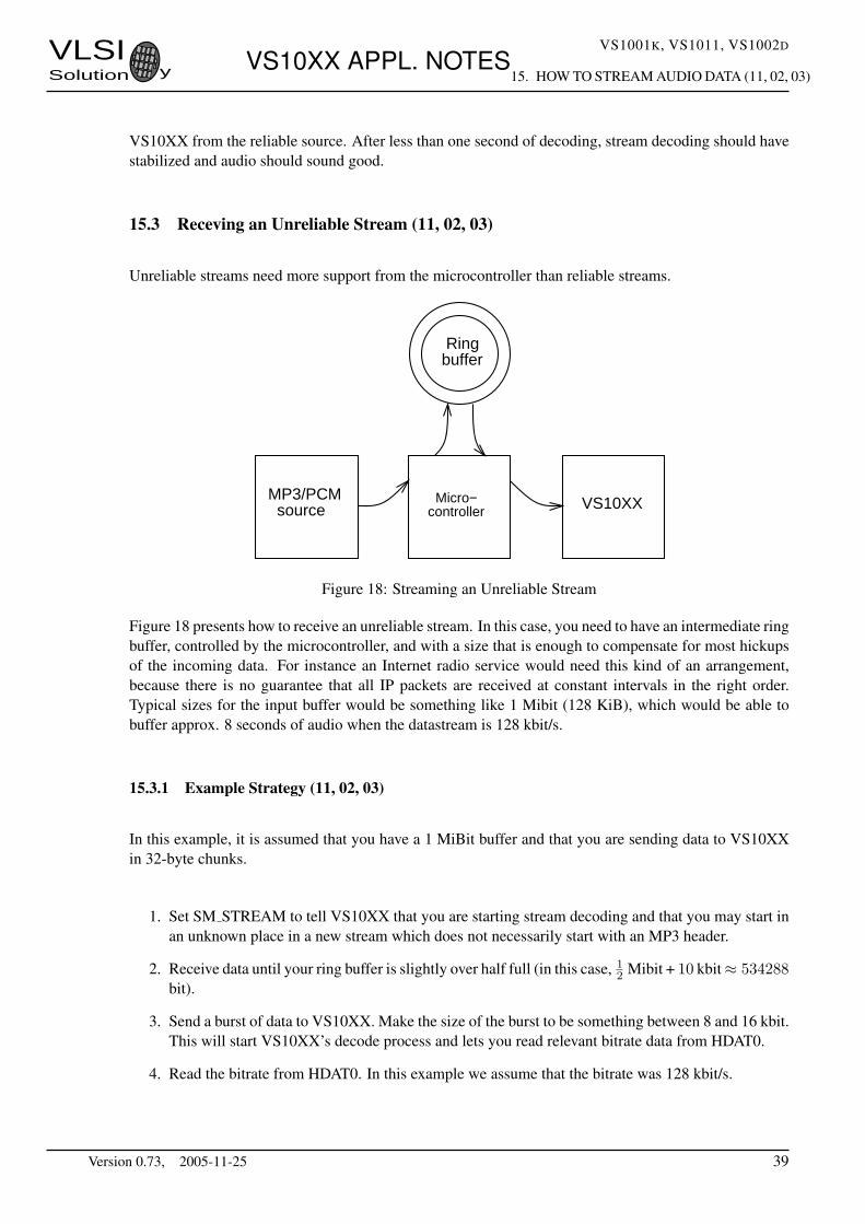
15.2 Receving a Reliable Stream (11, 02, 03)
VS10XXMP3/PCM source
Micro−controller
Figure 17: Streaming a Reliable Stream
As can be seen from Figure 17, receiving a reliable stream is relatively simple: data is send directly to
Version 0.73, 2005-11-25 38
VLSISolution y VS10XX APPL. NOTES
VS1001K, VS1011, VS1002D
15. HOW TO STREAM AUDIO DATA (11, 02, 03)
VS10XX from the reliable source. After less than one second of decoding, stream decoding should havestabilized and audio should sound good.
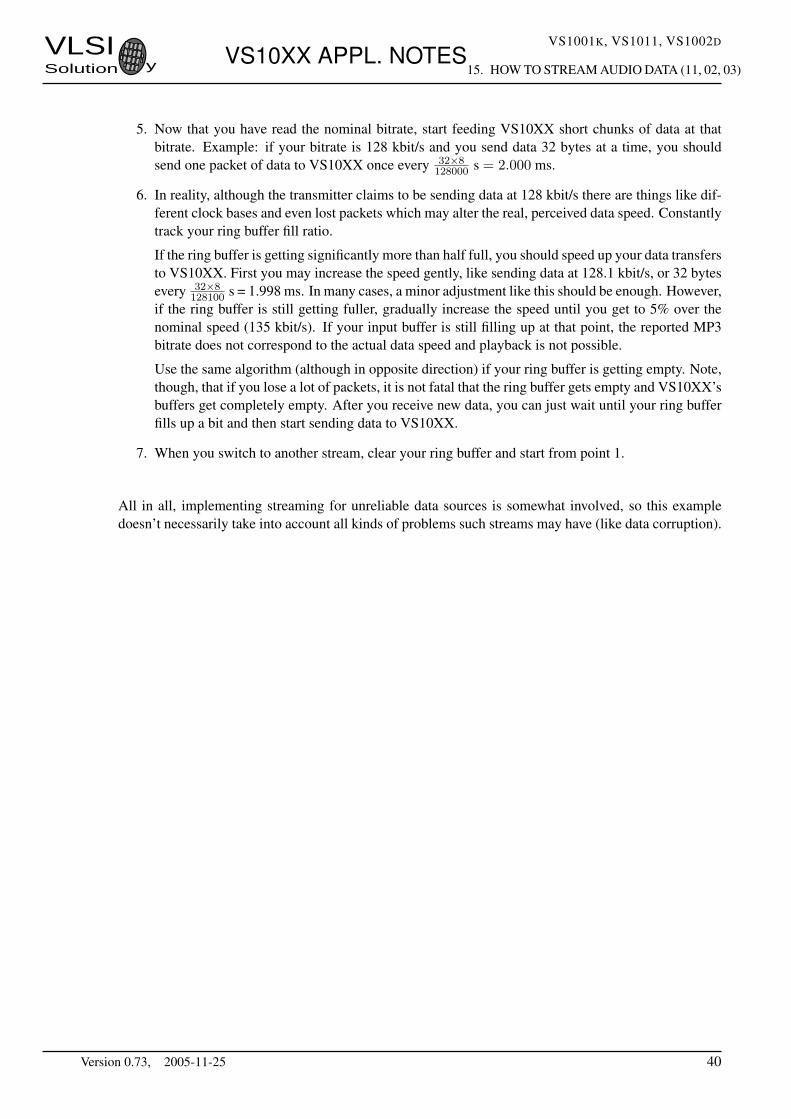
15.3 Receving an Unreliable Stream (11, 02, 03)
Unreliable streams need more support from the microcontroller than reliable streams.
VS10XXMP3/PCM source
Micro−controller
Ringbuffer
Figure 18: Streaming an Unreliable Stream
Figure 18 presents how to receive an unreliable stream. In this case, you need to have an intermediate ringbuffer, controlled by the microcontroller, and with a size that is enough to compensate for most hickupsof the incoming data. For instance an Internet radio service would need this kind of an arrangement,because there is no guarantee that all IP packets are received at constant intervals in the right order.Typical sizes for the input buffer would be something like 1 Mibit (128 KiB), which would be able tobuffer approx. 8 seconds of audio when the datastream is 128 kbit/s.
15.3.1 Example Strategy (11, 02, 03)
In this example, it is assumed that you have a 1 MiBit buffer and that you are sending data to VS10XXin 32-byte chunks.
1. Set SM STREAM to tell VS10XX that you are starting stream decoding and that you may start inan unknown place in a new stream which does not necessarily start with an MP3 header.
2. Receive data until your ring buffer is slightly over half full (in this case, 12 Mibit + 10 kbit≈ 534288
bit).
3. Send a burst of data to VS10XX. Make the size of the burst to be something between 8 and 16 kbit.This will start VS10XX’s decode process and lets you read relevant bitrate data from HDAT0.
4. Read the bitrate from HDAT0. In this example we assume that the bitrate was 128 kbit/s.
Version 0.73, 2005-11-25 39
VLSISolution y VS10XX APPL. NOTES
VS1001K, VS1011, VS1002D
15. HOW TO STREAM AUDIO DATA (11, 02, 03)
5. Now that you have read the nominal bitrate, start feeding VS10XX short chunks of data at thatbitrate. Example: if your bitrate is 128 kbit/s and you send data 32 bytes at a time, you shouldsend one packet of data to VS10XX once every 32×8
128000 s = 2.000 ms.
6. In reality, although the transmitter claims to be sending data at 128 kbit/s there are things like dif-ferent clock bases and even lost packets which may alter the real, perceived data speed. Constantlytrack your ring buffer fill ratio.
If the ring buffer is getting significantly more than half full, you should speed up your data transfersto VS10XX. First you may increase the speed gently, like sending data at 128.1 kbit/s, or 32 bytesevery 32×8
128100 s = 1.998 ms. In many cases, a minor adjustment like this should be enough. However,if the ring buffer is still getting fuller, gradually increase the speed until you get to 5% over thenominal speed (135 kbit/s). If your input buffer is still filling up at that point, the reported MP3bitrate does not correspond to the actual data speed and playback is not possible.
Use the same algorithm (although in opposite direction) if your ring buffer is getting empty. Note,though, that if you lose a lot of packets, it is not fatal that the ring buffer gets empty and VS10XX’sbuffers get completely empty. After you receive new data, you can just wait until your ring bufferfills up a bit and then start sending data to VS10XX.
7. When you switch to another stream, clear your ring buffer and start from point 1.
All in all, implementing streaming for unreliable data sources is somewhat involved, so this exampledoesn’t necessarily take into account all kinds of problems such streams may have (like data corruption).
Version 0.73, 2005-11-25 40
VLSISolution y VS10XX APPL. NOTES
VS1001K, VS1011, VS1002D
16. SPI BOOT (02)
16 Spi Boot (02)
16.1 Introduction (02)
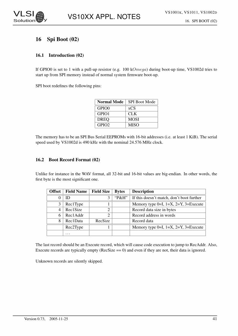
If GPIO0 is set to 1 with a pull-up resistor (e.g. 100 kOmega) during boot-up time, VS1002d tries tostart up from SPI memory instead of normal system firmware boot-up.
SPI boot redefines the following pins:
Normal Mode SPI Boot ModeGPIO0 xCSGPIO1 CLKDREQ MOSIGPIO2 MISO
The memory has to be an SPI Bus Serial EEPROMs with 16-bit addresses (i.e. at least 1 KiB). The serialspeed used by VS1002d is 490 kHz with the nominal 24.576 MHz clock.
16.2 Boot Record Format (02)
Unlike for instance in the WAV format, all 32-bit and 16-bit values are big-endian. In other words, thefirst byte is the most significant one.
Offset Field Name Field Size Bytes Description0 ID 3 “P&H” If this doesn’t match, don’t boot further3 Rec1Type 1 Memory type 0=I, 1=X, 2=Y, 3=Execute4 Rec1Size 2 Record data size in bytes6 Rec1Addr 2 Record address in words8 Rec1Data RecSize Record data
Rec2Type 1 Memory type 0=I, 1=X, 2=Y, 3=Execute. . .
The last record should be an Execute record, which will cause code execution to jump to RecAddr. Also,Execute records are typically empty (RecSize == 0) and even if they are not, their data is ignored.
Unknown records are silently skipped.
Version 0.73, 2005-11-25 41
VLSISolution y VS10XX APPL. NOTES
VS1001K, VS1011, VS1002D
17. VS10XX DIFFERENCES
17 VS10XX Differences
This chapter describes changes between different generations of VS10XX.
17.1 Basic Features of VS1001k
• Low-power MPEG 1 & 2 audio Layer 3 (MP3) decoder.
• Supports all samplerates and bitrates of MP3, including Variable BitRate VBR.
• Operates as a slave co-processor.
• Low-power VS DSP2 processor core.
• Operates with a single clock 12..13 MHz or 24..26 MHz.
• On-Chip Stereo DAC with no phase error between channels.
• Stereo earphone amplifier capable of driving downto 30Ω load.
• Built-in ground buffer (except in SOIC-28 package).
• Separate 2.5 .. 3.6 V operating voltages for analog and digital.
• 4 KiB on-chip Instruction RAM and 0.5 KiB data RAM for user code and data.
• Serial control and data interfaces allows connection with 8 pins.
• Minimun data connection requirement 6 pins and one AND port.
• Audio enhancer software and PCM decoder available at VLSI Solution’s web page.
17.2 Changes Between VS1001k and VS1011, 2003-09
• Downwards pin compatible with VS1001 when using old SCI mode.
• Plays also 8-bit and 16-bit mono and stereo WAV PCM files in addition to MP3 files.
• VS DSP2 core replaced with more powerful VS DSP4 core.
• More flexible clock and voltage range allows for more special effects (TBD later).
• User software RAM instruction space increased from 4 KiB to 5 KiB.
• New SCI/SDI mode activated with SM SDINEW.
– Compatibility mode: SCI/SDI work exactly as before, with old pins and BSYNC.– New mode: Depending on application, only 4 or 5 pins required for both SCI and SDI com-
pared to the nominal 8 pins of old mode. No BSYNC generation is needed.
• Power-on and power-off audio clicks have been eliminated.
• New bass enhancement offers a 1. . . 15 dB bass boost with a cut-off frequency of 30. . . 150 Hz.
• Streaming mode allows for receiving network audio where user cannot control sender’s speed.
• Greatly enhanced data synchronization and error resistance for MP3s.
• Random access sync mode makes fast forward / reverse easy to implement.
Version 0.73, 2005-11-25 42
VLSISolution y VS10XX APPL. NOTES
VS1001K, VS1011, VS1002D
17. VS10XX DIFFERENCES
• 4 General I/O pins that can be used by user software.
• Inadvertent starting of memory test as well as other tests prevented with new SCI MODE registerbit SCI TESTS.
• SPI timing is slightly different.
17.3 Changes Between VS1011 and VS1002d, 2003-09
• Downwards pin compatible with VS1001 when using old SCI mode.
• MP3+V (PlusV) playback, with stereo bitrates as low as 48 kbit/s.
• Mono WAV IMA ADPCM decoding added to MP3 and WAV PCM decoding.
• 2 KiB extra data memory if PlusV is not active.
• Microphone amplifier followed by single-channel multi-rate A/D converter allows for voice record-ing.
• System firmware supports recording in IMA ADPCM format.
• Two general-purpose timers for user programs.
• High-speed UART provided.
– Provides an interface to VLSI Solution’s VSIDE Integrated Development Environment.– Can be used for loading code and booting.– Can also be used for other user-specified data transfers.
• SPI Eeprom Boot allows building very simplistic standalone players with minimum functionality.
Version 0.73, 2005-11-25 43
VLSISolution y VS10XX APPL. NOTES
VS1001K, VS1011, VS1002D
18. DOCUMENT VERSION CHANGES
18 Document Version Changes
This chapter describes the most important changes to this document.
Version 0.75, 2005-04-21
• ESD section moved to new app. note.
Version 0.74, 2005-11-21
• General updates (ESD, Recording, Streaming)
Version 0.73, 2005-11-21
• Updated Chapter 2.2, “Using an External Clock (all)”.
Version 0.72, 2004-09-23
• Added Chapter 14.3.2, “IMA ADPCM and VS1002d Considerations”.
Version 0.71, 2004-06-07
• Corrected codes for “Writing to SDI” (Chapters 4.7 and 4.8).
• Removed SM JUMP from Chapter 15.3.1.
• Fixed schematics for declicking VS1001k (Chapter 9)
Version 0.70, 2004-05-13
• Updated whole document to VS1002d, separated VS1002c specific Chapter 14.3.1.
• Removed SM JUMP from Chapter 15.3.1.
Version 0.61, 2004-03-11
• Added Chapter 14.2, Microphone Connection (02).
• Added Chapter 15, How to Stream Audio Data (11, 02).
Version 0.73, 2005-11-25 44
VLSISolution y VS10XX APPL. NOTES
VS1001K, VS1011, VS1002D
19. CONTACT INFORMATION
19 Contact Information
VLSI Solution OyHermiankatu 6-8 CFIN-33720 Tampere
FINLAND
Fax: +358-3-316 5220Phone: +358-3-316 5230
Email: [email protected]: http://www.vlsi.fi/
Note: If you have questions, first seehttp://www.vlsi.fi/vs1001/faq/http://www.vlsi.fi/vs1011/faq/http://www.vlsi.fi/vs1002/faq/
Version 0.73, 2005-11-25 45