web viewlatha mathavan engineering college, madurai. department of electrical & electronics...
TRANSCRIPT

LATHA MATHAVAN ENGINEERING COLLEGE, MADURAIDEPARTMENT OF ELECTRICAL & ELECTRONICS ENGINEERING
EE6502 MICROPROCESSORS AND MICROCONTROLLERSIII YEAR/V SEMESTER
OBJECTIVES:To study the Architecture of uP8085 & uC 8051To study the addressing modes & instruction set of 8085 & 8051.To introduce the need & use of Interrupt structure 8085 & 8051.To develop skill in simple applications development with programming 8085 & 8051 To introduce commonly used peripheral / interfacing
UNIT I 8085 PROCESSOR 9Hardware Architecture, pinouts – Functional Building Blocks of Processor – Memory organization – I/O ports and data transfer concepts– Timing Diagram – Interrupts.UNIT II PROGRAMMING OF 8085 PROCESSOR 9Instruction -format and addressing modes – Assembly language format – Data transfer, data manipulation& control instructions – Programming: Loop structure with counting & Indexing – Look up table - Subroutine instructions - stack.UNIT III 8051 MICRO CONTROLLER 9Hardware Architecture, pintouts – Functional Building Blocks of Processor – Memory organization – I/O ports and data transfer concepts– Timing Diagram – Interrupts-Comparison to Programming concepts with 8085.UNIT IV PERIPHERAL INTERFACING 9Study on need, Architecture, configuration and interfacing, with ICs: 8255 , 8259 , 8254,8237,8251, 8279 ,- A/D and D/A converters &Interfacing with 8085& 8051.UNIT V MICRO CONTROLLER PROGRAMMING & APPLICATIONS 9Data Transfer, Manipulation, Control Algorithms& I/O instructions – Simple programming exercises keyboard and display interface – Closed loop control of servo motor- stepper motor control –Washing Machine Control.
TOTAL : 45 PERIODSOUTCOMES:
Ability to understand and analyse, linear and digital electronic circuits.To understand and apply computing platform and software for engineering problems.
TEXT BOOKS:1. Krishna Kant, “Microprocessor and Microcontrollers”, Eastern Company Edition,Prentice Hall of India, New Delhi , 2007.2. R.S. Gaonkar, „Microprocessor Architecture Programming and Application‟, with8085, Wiley Eastern Ltd., New Delhi, 2013.3. Soumitra Kumar Mandal, Microprocessor & Microcontroller Architecture, Programming & Interfacing using 8085,8086,8051,McGraw Hill Edu,2013.REFERENCES:1. Muhammad Ali Mazidi & Janice Gilli Mazidi, R.D.Kinely „The 8051 Micro Controller and Embedded Systems‟, PHI Pearson Education, 5th Indian reprint, 2003.2. Valder – Perez, “Microcontroller – Fundamentals and Applications with Pic,” Yeesdee Publishers, Tayler & Francis, 2013.

QUESTION BANK
EE 6502 / Microprocessor and Microcontroller
Unit I- 8085 Processor
PART-A (2-Marks)YEAR/SEM : III/V
1. What is meant by Level triggered interrupt? Which are the interrupts in 8085 level triggered?
Triggering is used to enable the signal to make circuit active or to do its function. It is normally by using the clock signal . It can be a negative level triggering in which the circuit is active when the clock signal is low or a positive level triggering in which the circuit is active when the clock signal is high.
RST 6.5 ,RST 5.5 INTR, TRAP are the level triggered interrupts
2. To obtain a 320ns clock what should be the input clock frequency? What is the frequency of clock signal at CLK OUT?
The input clock frequency must be 6.25 MHZ to obtain 320ns.The input clock signal frequency at CLK OUT is 3 MHZ.
3. What is TRAP interrupt and its significance?
TRAP is a Non Maskable Interrupt. It means that it is unaffected by any mask or interrupt enable. It has the highest priority. It is edge and level triggered which means it must go high and remain high until it is acknowledged.
4. Define the function of parity flag and zero flag in 8085? May/June 2012
Parity flag is defined by the number of ones present in the accumulator. After an arithmetic or logical operation if the result has an even number of ones. i.e. even parity the flag is set ,if the parity is odd flag is reset.
Zero flag sets if the result of operation in ALU is zero and flag resets if result is non zero.
5. What is the function of program counter in 8085? April /May 2013
It is a special purpose register which at a given time stores the address of the next instruction to be fetched. It acts as a pointer to the next instruction.
6. Write down the control and status signals of 8085. Nov/Dec 2012
Two Control signals and three status signals
Control signals: RD and WR Status signals: IO/M, S1, S2
7. Specify the size of data, address, memory word and memory capacity of 8085 microprocessor.(A/M’11)
8085 operate 8bit data. The 8085 has 16 address lines, hence it can access (216
) 64 Kbytes of memory

8. Draw the schematic of latching low order address bus in 8085 microprocessor. (N/D’11)
9. What are the flags used in 8085? NOV/Dec 2013
Sign, Zero, Parity, Carry and Auxiliary Carry
10. What is ALE? ? NOV/Dec 2013
ALE is Address Latch Enable.
The ALE signal goes high at the beginning of each machine cycle indicating the availability of the address on the address bus, and the signal is used to latch the loworder address bus.
11. Specify the function of Address bus and the direction of the information flow on the address bus? Nov./Dec 2012 (R 2004)
The address is an identification number used by the microprocessor to identify or access a memory location or I / O device. It is an output signal from the processor. Hence the address bus is unidirectional.
12. What do you mean by masking the interrupt? How it is activated in 8085?
Masking is preventing the interrupt from disturbing the current program execution. When the processor is performing an important job (process) and if the process should not be interrupted then all the interrupts should be masked or disabled. In processor with multiple 'interrupts, the lower priority interrupt can be masked so as to prevent it from interrupting, the execution of interrupt service routine of higher priority interrupt
13. What are the two limitations of the 8085 that may not allow it to qualify entirely as a μP?
i. The lower order address buses (AD7-AD0) need to be demultiplexedii. Appropriate control signals need to be generated to interface peripherals
14. Define T-state and in which T-cycle the ALE signal is activated?
T-State is defined as one subdivision of the operation performed in one clock period. These subdivisions are internal states synchronized with the system clock, and each T-State is precisely equal to one clock period.

15. What is a flag?
The data conditions, after arithmetic or logical operations, are indicated by setting or resetting the flip-flops called flags.
16. Differentiate Software and Hardware interrupts.
The Software interrupt is initiated by the main program, but the hardware interrupt is initiated by the external device. In 8085, Software interrupts cannot be masked or disabled, but in hardware interrupts except TRAP all other interrupts can be masked.
17. Define i) Instruction cycle ii) Machine cyclei) The sequence of operations that a processor has to carry out while executing the
instruction is called Instruction cycle. Each instruction cycle of a processor indium consists of a number of machine cycles.
ii) The processor cycle or machine cycle is the basic operation performed by the processor. To execute an instruction, the processor will run one or more machine cycles in a particular order.
18. What is the need for a timing diagram?The timing diagram provides information regarding the status of various signals, when a
machine cycle is executed. The knowledge of timing diagram is essential for system designer to select matched peripheral devices like memories, latches, ports, etc., to form a microprocessor system.
19. Why are the program counter and the stack pointer 16-bit registers?Memory locations for the program counter and stack pointer have 16-bit addresses. So
the PC and SP have 16-bit registers.
20. List the main applications of 8 bit microprocessors?
(i) LCD (ii) Microcomputer (iii) Keyboard display21. Explain the instruction SIM and RIM?
RIM: Read Interrupt Mask- It is a single byte instruction. This Instruction Copies or loads the accumulator with eight bits indicating the current status of the interrupt masks. It also reads the serial data through the SID pin.
SIM: Set Interrupt Mask- It is a single byte instruction. This instruction read the content of the accumulator and enable or disable the interrupt according to the content of the accumulator. It also sends out serial data through the SOD pin.
22. What is the use of an Instruction Decoder?
The processor first fetches the opcode of instruction from memory and stores this opcode in the instruction register and then to the instruction decoder. The instruction decoder decodes it and accordingly gives the timing and control signals which control the register, data buffers, ALU and external peripheral signals depending on the nature of the instruction.
23. What do you mean by stack pointer
The stack pointer is a reserved area of the memory in the RAM where temporary information may be stored. A 16- bit stack pointer is used to hold the address of the most of the stack entry.
24. State the machine cycle of 8085?
Opcode fetch, Memory Read, Memory Write, I/O Read, I/O Write, Interrupt acknowledgement and Bus idle

25. State the five interrupt signals of 8085 INTR, INTA, RESET, HOLD and READY.
26. Explain the General Purpose Registers?
There are six general purpose registers – B, C, D, E, H & L. These registers can be used as separate 8 bit registers or 16 – bit register pairs as BC, DE and HL. When used in register pair mode, the higher order byte resides in the first register and the lower order byte in the second register. HL pair also functions as a data pointer or memory pointer. These are used to store the data and retrieved during any arithmetic and logical operation.
27. What is meant by Enable interrupt and disable interrupt?
Enable interrupt ( EI) – it is a single byte instruction which is used to set the interrupt enable flip flop and enable the interrupt process
Disable Interrupt ( DI) - it is a single byte instruction which is used to reset the interrupt enable flip flop and disables the interrupt process
28. What is the function of Data transfer?These instructions perform the following six operations:
Loads an 8 bit number in a register Loads 16 bit number in a register pair Copy from a register to another register
Copy between register and memory
Copy between I/O and accumulator
Copy between registers and stack memory
29. Difference between Memory mapped I/O and peripheral Mapped I/O?Characteristics Memory mapped I/O peripheral Mapped I/ODevice address 16 bit 8 bitControl signals for input/ _____ _____ ___ ___output MEMR / MEMW IOR / IOWInstructions used STA, LDA, ADD M, SUB M IN & OUTData transfer Between any registers and Between I/O and the
I/O accumulatorMaximum number of I/Os The memory map (64k) is The I/O map is independent ofpossible shared between I/Os and the memory map, 256 input
memory devices and 256 outputdevices can be connected
Execution Speed 13 T states ( STA, LDA) 10 T states7 T states ( MOV M, R)
30. Define CLOCK OUT and RESET OUT?CLOCK OUT: this signal can be used as the system clock for other devices
RESET OUT: This signal indicates that the MPU is being reset. The signal can be used to reset other devices.

UNIT – II: PROGRAMMING OF 8085 PROCESSOR
PART – A
1. What is the different control machine control instructions used in 8085 microprocessor? M/J 2013
EI-Enable InterruptDI-Disable interruptNOP- No operationHLT- Halt, SIM, RIM.
2. What is the function of stack? M/J 2013Stack is s portion of Read /Write memory location set aside by the user for the purpose of
storing the information temporarily. When the information is written on the stack the operation is PUSH and when the information is read from the stack it is POP. The type of operation performed in stack is LIFO( last in first out)
3. Mention the similarity and difference between compare and Subtract instructions (M/J 2014)COMPARE:
This instruction compares the given numbers by subtracting it and gives the result if the numberis greater than, lesser than or equal to the status of sign and carry flag will be affected.SUBTRACT:
This instruction subtracts the two given numbers and the flag registers will not be affected.
4. State the purpose and importance of NOP instruction. M/J 2014NOP – No operation This instruction does not perform any operation. It can also be used to
make the clock signals to go in wait state that is delay time can be increased.
5. What are the types of addressing modes of 8085.M/J2012, N/D 2013?
1. Immediate2. Direct3. Register4. Indirect5. Implied
6. What is the use of branching instructions? Give examples. M/J2012These instructions allow the processor to change the sequence of the program either
conditionally or unconditionally or under certain test conditions. These include branch instructions, subroutine call and return instructions.7. State the function of given 8085 instruction: JP, JPE, JPO, JNZ. (A/M’11)
JP – 16 bit Address – Jump on Plus JPE – 16 bit Address – Jump on Even Parity
JPO – 16 bit address – Jump on Odd Parity JNZ – 16 bit address – Jump on No Zero

8. How is PUSH B instruction executed? Find the status after the execution (A/M’11)
This instruction decrements SP by one and copies the higher byte of the register pair into the memory location pointed by SP. Then decrements the SP again by one and copies the lower byte of the register pair into the memory location pointed by SP.
Ex: SP=2000H, DE=1050H
9. Why do we need look up table? (N/D’11)To store the complex parameters in the program memory. It reduces computational complexity. Eg:
SIN table.10. How are the 8085 instructions classified according to the functional categories? (N/D’11)
Data Transfer, Arithmetic, Logical, Branching, Machine Control.11. What is a stack in an 8085 microcomputer system? N/D 2012
Stack is s portion of Read /Write memory location set aside by the user for the purpose of storing the information temporarily. When the information is written on the stack the operation I s PUSH and when the information is read from the stack it is POP. The type of operation performed in stack is LIFO last in first out.12. What is indexing? N/D 2012
Indexing allows the programmer to point or refer the data stored in sequential memory locations one by one.
13. Give two examples for two byte and three byte instruction. M/J 2012 (R2004)1. MVIA, 082. IN CO……..2 byte instruction1. LDA 45002. STA 5000……3 byte instruction
14. What happens when the RET instruction at the end of the subroutine is executed? N/D 2012This instruction pops the return address (address of the instruction next to the CALL instruction
in the main program) from the stack and loads program counter with this return address. Thus transfers program control to the instruction next to Call in the main program.
15. What are the instructions associated with the subroutine. N/D2013
CALL 16 bit address: The program sequence is transferred to the address specified by the operand. Before the transfer, the address of the next instruction to CALL( the contents of the program counter) is pushed to the stack.

RET - RETURN: The program sequence is transferred from the subroutine to the calling program. The two bytes from the top of the stack are copied into the program counter and the program execution begins at the new address. The instruction is equivalent to POP program counter.
16. What is the significance of ‘XCHG’ and ‘SPHL’ instructions?‘XCHG’-Exchange the contents of HL register pair with DE register pair ie the contents of register
H are exchanged with the contents of register D and the contents of register L are exchanged with the contents of register E
SPHL-store the contents of HL register pair to the stack pointer. The contents of H register provide the higher order address and the contents of L register provide the low order address. The contents of H and L registers are not altered
17. What do you mean by Looping, Counting and Indexing?Looping: In this tech the program is instructed to execute certain set of instructions repeatedly
to execute a particular task number of times.Counting: This tech allows programmer to count how many times the ins of instruction are executed. Indexing: This tech allows programmer to point or refer the data stored in sequential memory location one by one.
18. Show the different instruction formats used in 8085. Give examples(i) One byte instruction –CLR A (ii) Two byte instruction -MVIA, 00 (iii) Three byte instruction-STA 500019. Define Opcode and operand?
The operation to be performed is called Opcode. The data to be operated is called operand.20. Give the difference between JZ and JNZ?
JZ change the program sequence to the location specified by the 16-bit address if the zero flag is set and JNZ change the program sequence to the location specified by the 16-bit address if the zero flag is reset.21. Explain the need of software interrupt?
Executing a group of instruction number of times can generate the time delays in few microseconds. These software timers are called time delay or software delays. It is necessary to keep time delays between 2 transitions.22. What is subroutine?
A Subroutine is a group of instructions which performs a particular subtask, which is executed number of times. It is written separately. The microprocessor executes the subroutine by transferring program control to the subroutine program. After completion the program control is returned back to the main program. It is a very important technique in designing software for microprocessor systems because it eliminates the need to write a subtask repeatedly: thus it uses memory more efficiently.
23. Differentiate between CALL / RET and PUSH / POP?
S.No CALL / RET PUSH / POP1 These instructions are used for the These instructions are used to store register data
execution of subroutine temporarily in memory2 CALL instruction stores the address of the PUSH instruction stores register contents in the
next instruction stack3 RET instructions loads the address from POP instruction gets the register content from
stack into program counter the stack

24.What is meant by immediate addressing mode?In an immediate addressing mode 8 or 16 bit data can be specified as a part of instruction. ‘I’
indicates the immediate addressing mode. Eg; MVI A, 20 H 25. What is meant by register addressing mode?
The register addressing mode specifies the source operand, destination operand, or both to be contained in an 8085 registers. This results in faster execution, since it is not necessary to access memory locations for operand. Eg : MOV A, B
26. What is meant by direct addressing mode?The direct addressing mode specifies the 16 bit address of the operand within the instruction itself.
The 2nd
and 3rd
bytes of the instruction contain this 16 bit address.
Eg: LDA 2050 H27. How does the microprocessor know how and when to start?
As soon as the Reset key is pushed, the program counter places the memory address 0000H on the address bus, the instruction at that location is fetched and the execution of the key monitor program begins. Therefore the key monitor program is stored on page 00H
28.What happens in a single board microcomputer when the power is turned on and the
Reset key is pushed?
When the power is turned on, the monitor program stored either in EPROM or ROM comes alive. The reset key clears the program counter and the program counter holds the memory address 0000H. some system automatically reset when the power is turned ON ( called power-on Reset)29. What is an assembler?
An assembler is a program that translates the mnemonics into their machine code. It is generally not available on a single board microcomputer.

UNIT – III: 8051 MICROCONTROLLER
PART - A
1. Give the memory size of 8051microcontroller. ( April/may -2010)The 8051 microcontroller consists of
4096 bytes On-chip program memory(ROM) 128 bytes On-chip data memory(RAM)
2. Give the details of PSW register in 8051. ( April/may -2010, May/June -2012, May/June -2014)
3. List the alternative functions assigned to Port 3 pins of 8051 microcontroller (April/may -2011)
The alternative functions of PORT 3 pins are:
PINS ALTERNATIVE FUNCTIONSP 3.0 (RXD) Serial data InputP 3.1 (TXD) Serial data OutputP 3.2 (INT0) External Interrupt 0P 3.3 (INT1) External Interrupt 1P 3.4 (T0) External timer 0 InputP 3.5 (T1) External timer 1 InputP 3.6 (WR) External memory write pulseP 3.7 (RD) External memory read pulse
4. Mention the size of DPTR and Stack Pointer in 8051 microcontroller. (April/may - 2011)
The Data Pointer (DPTR) is a 16 bit data Register and Stack pointer (SP) is 8 bitRegister.

5. What are the main features of 8051 microcontroller? (May/June -2012)The features are:
Single_supply +5 volt operation using HMOS technology. 4096 bytes program memory on chip (not on 8031) 128 data memory on chip. Four register banks.
Two multiple mode,16-bittimer/counter.
Extensive boolean processing capabilities.
64 KB external RAM size
6. What are the addressing modes of 8051? (May/June -2013, Nov/Dec-2011) The addressing modes of 8051 are:
a. Immediate.b. Register.c. Register indirect.d. Direct.e. Indexed.
7. What is the function of R register in 8051? (May/June -2013)The 8051 uses 8 "R" registers which are used in many of its instructions. These "R"
registers are numbered from 0 through 7 (R0, R1, R2, R3, R4, R5, R6, and R7). These registers are generally used to assist in manipulating values and moving data from one memory location to another.
8. Mention the purpose of PSEN and EA in 8051 microcontroller. (May/June -2014) PSEN:
If external ROM is used for storing program then a logic zero (0) appears on it every time the microcontroller reads a byte from memory.
EA:
By applying logic zero to this pin, P2 and P3 are used for data and address transmission with no regard to whether there is internal memory or not. It means that even there is a program written to the microcontroller, it will not be executed. Instead, the program written to external ROM will be executed. By applying logic one to the EA pin, the microcontroller will use both memories, first internal then external (if exists).
9. List the interrupt sources in 8051. (May/June -2014) There are 5 interrupts which occurs in 8051
3 Internal Interrupts provided by Timer flag 0Timer flag 1Serial port interrupt (R1 /T1)
2 External Interrupt provided by
( PORT PIN 3.2)

10. List the on-chip peripherals of 8051 microcontroller. (Nov/Dec-2011) Program memory data memory 4 parallel ports
serial port timers and
interrupt controller11. How many ports are bit addressable in 8051 microcontroller. (Nov/Dec-
2012) P0, P1, P2 & P3 (all the four ports are bit addressable)12. Give an example of DA instruction of 8051 microcontroller. (Nov/Dec-2012)
DA A
Decimal Adjust of the accumulator It occupies 1 byte and has 12 Oscillator period
13. Explain the mode3 of 8051 serial ports? (Nov-2009)
In this mode,11 bits are transmitted(through TXD)or received(through RXD):a start bit(0), 8 data bits(LSB first),a programmable 9th data bit ,& a stop bit(1).In fact ,Mode3 is the same as Mode2 in all respects except the baud rate. The baud rate in Mode3 is variable. In all the four modes, transmission is initiated by any instruction that uses SBUF as a destination register. Reception is initiated in Mode0 by the condition RI=0&REN=1.Reception is initiated in other modes by the incoming start bit if REN=1.
14. Write A program to perform multiplication of 2 no’s using 8051? (NOV-2009) MOV A, data 1
MOV B, #data
2 MUL AB
MOV DPTR, #5000
MOV @DPTR, A (lower value)
INC DPTR
MOV A, B
MOVX @ DPTR, A
15. What is memory mapping? (may/june 2011)
Memory mapping may refer to: Memory-mapped file, also known as mmap()Memorymapped I/O, an alternative to port I/O; a communication between CPU and peripheral device using the same instructions, and same bus, as between CPU and memory Virtual memory, technique which gives an application program the impression that it has contiguous working memory, while in fact it is physically fragmented and may even overflow on to disk storage.
16. Write short notes on interrupt priority.ISR-Interrupt service routine stores all the levels that are currently being serviced.

17. List the operating modes of 8255A PPI?(i) Two 8-bit ports (A and B)
(ii) Two 4-bit ports (Cu and CL)
(iii) Data bus buffer
(iv) Control logic
18. What is USART?USART is an integrated circuit. It is a programmable device; its function and specifications for
serial I/O can be determined by writing instructions in its internal registers.
19. Name any four additional hardware features available in microcontrollers when compared to microprocessors.
• Two multiple mode• 16 bit timers/counters• Four register banks• integrated Boolean processor•
20. Write the steps necessary to initialize a counter in write operations?• Write a control word into the control register• Load the low-order address byte• Load the high order byte
UNIT – IV: PERIPHERAL INTERFACINGPART A
1. What are the different ways to end the interrupt execution in 8259 PIC? (A/M’11)
AEOI (Automatic End of Interrupt) mode the ISR bit is reset at the end of the second INTA pulse. Otherwise, the ISR bit remains set until the issue of an appropriate EOI command at the end of the interrupt subroutine.
2.What is the function of Scan section in 8279 programmable keyboard/Display controller?(A/M’11)
Scan section which has two modes (i) Encoded Mode (ii) Decoded ModeEncoded Mode: In this mode, Scan counter provides a binary count from 0000 to 1111 the four scan lines (SC3 – SC0) with active high outputs.Decoded Mode: The internal decoder decodes the least significant 2 bits of binary count andprovides four possible combinations on the scan lines (SC3- SC0) : 1110,1101,1011 and 0111.
3. Draw the ‘mode word’ format of 8251 USART. (N/D’11) (N/D’12)

4. State the use of ISR and PR registers in 8259 PIC. (N/D’11)
ISR- Interrupt service Register Stores all the levels that are currently being serviced.PR– Priority Resolver determines the priorities of the bits set in the IRR (Interrupt Request register). The bit corresponding to the highest priority interrupt input is set in the ISR during the INTA input.
5. What are the salient features of INTEL 8259 Programmable interrupt controller? M/J 14
1. It manage eight Priority interrupt request.2. The interrupt vector addresses are programmable.3. The8259 are programmed to accept either the level triggered or edge
triggered Interrupt request.4. The interrupt can be masked or unmasked individually.5. 8259 helps to get the information of pending interrupts, in-service interrupts
and masked interrupts
6. How data is transmitted in asynchronous serial communication? M/J ‘14Data is transmitted by setting transmission enable bit in the command
instruction. When transmitter is enabled and CTS =0 the transmitter is ready to transfer data on Tx D line. The data bits is framed with one start bit and stop bits and then transmitted.
7. What are the applications of D/A converter interfacing with 8255? M/J ‘12Generating square, triangular and sine waveform, used in automatic process control
8. What is keyboard interfacing? M/J 12Keyboard interfacing is interfacing an input device. Push button switches are used.in
simple keyboard interface one input line is required to interface one key and this number will increase with number of keys. It is in the form of matrix with rows and columns and at the intersection a switch is present.
9. What are the different peripheral interfacing used with 8085 processor? M/J 13
8255PPI, 8279 Keyboard and display controller, 8251 USART, 8259 PIC and 8254 - timer10. What are the output terminals in USART 8251? M/
J 13 RD, WR11. What is the need for 8259 PIC?
It is necessary to solve multiple interrupt requests (more than five) we use an external device called a PIC. It is possible to increase the interrupt handling capacity of the microprocessor. When executing an interrupt an ISR can be serviced.
12. What are the basic modes of 8255? N/D 20131. BSR mode2. I/O mode which is operated in mode 0, mode 1 and mode 2
13. What are the operating modes of IC 8253 / 8254 Timer?There are 6 operating modes in IC 8254 Timer they areMode 0: Interrupt on Terminal Count

Mode 1: Hardware – Triggered one shotMode 2 – Rate GeneratorMode 3 – Square wave generatorMode 4 – Software triggered strobeMode 5- Hardware triggered strobe
14. What is key de bouncing?The push button keys when pressed, bounces a few times, closing and opening the
contact before providing a steady reading. The reading taken during the bouncing period may be wrong. Therefore, microprocessor must wait until the key reach to a steady state known as key debounce.
15. What is the difference between A/D and D/A converters?Digital-to-analog is used to get a proportional analog voltage or current for the digital
data given out by the microprocessor. An ADC converts the input analog voltage levels to the corresponding discrete digital signals.
16. Define the following terms for D/A converters.i) Resolution: Resolution of a converter determines the degree of accuracy in conversion.It is equal to 1/2n.ii) Accuracy: Accuracy is the degree to which information on a map or in a digital database matches true or accepted values. Accuracy is an issue pertaining to the quality of data and the number of errors contained in a dataset or map.
iii) Monotonicity : If a clock has monotonicity, then each successive time reading from that clock will yield a time further in the future than the previous reading.iv)Conversion time: The time required by an analog to digital converter to fully convert and analog input sample.
17. List the features of 8279.(i) It has built in hardware to provide key debounce.(ii) It provides two output modes for display interface : Left and Right entry(iii) It provides three input modes for keyboard interface: Scanned keyboard
Mode, Scanned sensor matrix mode and strobed input mode.(iv) It provides multiplexed display interface with blanking and inhibit options. 18. How is DMA initiated?
When the IO device needs a DMA transfer, it will send DMA request signal to the DMA controller. The DMA controller in turn sends a HOLD request to the processor. When the processor receives a HOLD request, it will drive its tristated pins to high impedance state at the end for current instruction execution and send an acknowledge signal to the DMA controller. Now the DMA controller will perform DMA transfer
19. What are the different types of DMA?Cycle stealing (or Single transfer) DMA, Block transfer (or Burst Mode)
DMA and Demand transfer DMA.

20. What is Cycle stealing DMA?In Cycle stealing DMA, the DMA controller will perform one DMA transfer in
between instruction cycles (i.e. in this mode, the execution of one processor instruction and one DMA data transfer will take place alternatively).
21. What is the function of the GATE signal in timer 8254?In timer 8254, the GATE signal acts as a control signal to start, stop or
maintain the counting process. In modes 0, 2, 3, and 4 the GATE signal should remain high to start and maintain the counting process. In modes 1 and 5, GATE signal has to make low to high transitions to start the counting process and need not remain high to maintain the counting process.
22. What is meant by doubling the baud rate in the 8051? We can double the baud rate in 8051 using two ways
i) By doubling the crystal frequency.ii) By making SMOD bit in the PCON register from 0 to 1.
23. What is the function of C/T bit in TMOD register in timer in 8051?C/T bit in the TMOD register decides the timer/counter functioning as a counter or a timer. When C/T = 0, the timer mode is selected and the crystal is used as a source of frequency. When C/T =1, the counter mode is selected, it gets its pulse from outside the 8051. The counter counts up for each clock pulse applied at the pins of port 3
24.What is meant by Handshake signals in 8255 PPI?The MPU and peripherals operates at different speed; signals are exchanged prior to data transfer between the fast responding MPU and slow responding peripherals such as printer and data converters. These signals are called Handshake signals.
25.What is meant by Over Run error (OE), Parity error (PE) and framing error (FE) in 8251 PCI?
Over Run Error: The OE flag is set when the CPU does not read a character before the next one becomes available. It is reset by the Error reset (ER) bit in the command instruction. OE does not inhibit operation of the 8251. However the previously over run character is lost.
Parity Error (PE): The PE flag is set when a parity error is detected. It is reset by the ER bit of the command instruction. PE does not inhibit operation of the 8251.
Framing Error: The FE flag is set when a valid stop bit is not detected at the end of every character. It is reset by the ER bit of the command instruction. FE does not inhibit the operation of the 8251.
26.How does a serial communication classified?The serial communication are classified according to the direction and data
flow as Simplex transmission- data transmitted in only one direction, eg – transmission from a microcomputer to a printer.
Duplex Transmission – data flows in both direction. If data gets transmitted one way at a time called as half duplex and if data gets transmitted in both direction called as full duplex. Eg transmission between two computers, between a computer and a terminal.
27.What are the types of priority modes in 8259 PIC?Fully Nested Mode, Automatic rotation mode, specific rotation mode and end of

Interrupt.
28.What is meant by two key lockout and N key roll over in 8279?The keys are automatically de bounced and the keyboard can operate in two modes:
i) Two key Lock out – In this mode if two keys are pressed almost simultaneously, only the first key is recognized.ii) N key roll over- In this mode simultaneous keys are recognized and their codes are stored in the internal buffer; it can also be set up so that no key is recognized until one key remains pressed.
29.Explain the mode3 of 8051 serial ports? (Nov-2009)In this mode, 11 bits are transmitted (through TXD )or received (through
RXD):a start bit(0), 8 data bits(LSB first),a programmable 9th data bit ,& a stop bit(1).In fact ,Mode3 is same as Mode2 in all respects except the baud rate. The baud rate in Mode3 is variable. In all the four modes, transmission is initiated by any instruction that uses SBUF as a destination register. Reception is initiated in Mode0 by the condition RI=0 & REN=1.Reception is initiated in other modes by the incoming start bit if REN=1.
30.List the operating modes of 8255A PPI?(i) Two 8-bit ports (A and B)(ii) Two 4-bit ports (Cu and CL) (iii) Data bus buffer(iv) Control logic
31.Compare between Synchronous and Asynchronous Data transmission?
S.NO Synchronous Data Transmission Asynchronous Data transmission1 In this transmission, both transmitter In this transmission, both transmitter and
and receiver are synchronous with the receiver are not synchronous with thecommon CLK signals common clock (CLK), they use separate clock
signals2 In this mode, the framing bits are sent Framing bits are sent along with each
along with block ( at the beginning of character ( at the beginning and end of theblock) character)
3 The speed of the synchronous data The speed of the asynchronous datatransmission is higher than 20K bauds transmission is less than 20K bauds.
4 Framing information is SIM character Framing information is start and stop bits5 It is always implemented through It is implemented through software
hardware
UNIT – V: MICRO CONTROLLER PROGRAMMING & APPLICATIONS
PART – A
1. List the different types of 8051 instructions. ( April/may -2010, Nov/Dec-2011) The different types of 8051 instructions are:

a. Logical Instructionsb. Arithmetic Instructionsc. Data transfer Instructionsd. Branch Instructionse. Jump & CALL Instruction
2. What are the various operations performed by Boolean variable instructions of 8051?
Boolean variable instructions perform the following operationsBOOLEAN OPERATOR MNEMONICSAND(AND logical)OR(OR logical)
ANLORL
NOT(COMPLEMENT) CPLXOR(Exclusive OR logical) XRL
3. What is the operation of the given 8051 microcontroller instructions: XRL A, direct? (April/may -2011)XOR each bit of A with the same bit of the direct RAM address and the result is stored in A (Acc).
4. Draw the flow chart for the programming of serial port of 8051 (May/June -2012)
5. What are the applications of 8051 microcontroller? (May/June -2012) The applications of 8051 microcontroller are:• Automobile• Aeronautics• Mobile communication• Robotics• Remote sensing etc.,

6. How is the pulse generated from microcontroller for stepper motor control (May/June - 2013)
To cause the stepper to rotate, we have to send a pulse to each coil in turn. The 8051 does not have sufficient drive capability on its output to drive each coil, so there are a number of ways to drive a stepper, Stepper motors are usually controlled by transistor or driver IC like ULN2003. Driving current for each coil is then needed about 60mA at +5V supply.
7. Why do we need opto-isolator circuit between microcontroller and the stepper motor? (Nov/Dec-2011)
Opto-isolator are widely used to isolate the stepper motor’s EMF voltage and keep it form damaging the digital microcontroller system.
8. Why interfacing is needed for 1/0 devices? (Nov-2009])Generally I/O devices are slow devices. Therefore the speed of I/O devices does not match with the speed of microprocessor. And so an interface is provided between system bus and I/O devices.
9. What is the operation carried out when 8051 executes the instruction MOVC A, @ A + DPTR? (Nov-2007)
This instruction loads the accumulator from the contents of program memory whose address is given by the sum of the contents of accumulator and contents of DPTR register (A) ‹— ((A) + (DPTR))
10. Write program to load accumulator, DPH, &DPL using 8051? (Nov-2007) MOV A,#30MOV DPH, A MOV DPL, A
11. Write a program to perform multiplication of 2 numbers using 8051? (NOV-2009)
MOV A,#data 1MOV B,#data 2MUL ABMOV DPTR,#5000MOV @DPTR,A(lower value)INC DPTRMOV A,BMOVX @ DPTR,A
12. Write a program to mask the 0th &7th bit using 8051? (APRIL-2009) MOV A,#dataANL A,#81MOV DPTR,#4500MOVX @DPTR,A LOOP SJMP LOOP

14. Write a program to subtract 2 8-bit numbers &exchange the digits using 8051? MOV A,#9FMOV R0,#40 SUBB A,R0SWAP A
15. Explain PUSH and POP instructions in 8051.PUSH-The stack pointer is incremented by one. The contents of the indicated
variable is then copied into the internal RAM location addressed by the stack pointer. POP-Reverse of PUSH operation.
16. How many ports are bit addressable in an 8051 microcontroller?(N/D ‘12’)In 8051 there are many bit-addressable registers such as A (ACC), B, SCON,
PCON, TCON, p0, p1, p2, p3.
17. Write a program to find the 2’s complement using 8051?( NOV-2008) MOV A, R0CPL A INC A
18. Explain rotate instructions of 8051.RL A RLC A RR ARRC A
19. Explain DAA instruction of 8051.Decimal adjust accumulator for addition bytes
20. What does the mnemonics “LCALL” and “ACALL” stands for? (Nov/Dec-2012) There are two subroutine CALL instructions. They are LCALL (Long CALL) ACALL (Absolute CALL). Each increments the PC to the 1st byte of the instruction& pushes them in to the stack.
21. What are the use of PWM in motor control using microcontroller?The speed of the dc motor depends on the applied voltage. The average applied dc voltage and power can be varied using a technique called pulse width modulation. In this technique the dc power supply is not a voltage of fixed amplitude ie it is a pulsating DC voltage. By changing the pulse width we can change the applied power.
22. Calculate the reload value of timer1 for achieving a baud rate of 4800in 8051 for a crystal frequency of 11.0592MHz?
TH = 256 – k * Oscillatory frequency-------------------------------384 * Baud rate
= 256 – 1*11.0592*10E6 / 384*4800= 250 = FAH

23. List the features of ADC0804?i) 8-bit successive approximation ADCii) Access time is 135nsiii) Conversion time is 100µsiv) It has an on chip clock generatorv) It does not require any zero adjustmentvi) It operates on single 5V power supply.
24. What is the output of the program?MOV R0, AXRL A, # 3F HXRL A, R0The contents of A register will be 3F H and the contents of R0 will be the initial contents of A
25. What are the different addressing modes of microcontroller 8051? ( A/ M -2008)i) Register addressingii) Direct byte addressingiii) Register indirect addressingiv) Immediate addressingv) Register specificvi) Index
26. Give the PSW setting for making register bank 2 as default register bank in 8051 microcontroller ( M / J 2007)MOV PSW, #10 ; SELECT BANK 2MOV A, R0 ; (A) ‹— (R0) FROM BANK 2MOV PSW, #00 ; SELECT BANK 0CLR C ; CLEAR CARRYSUBB A, R1 ; A ‹— A- (R1) FROM BANK 0
The above program is to subtract the contents of R1 of BANK0 from the contents of RO of Bank 2.
UNIT – І 16 MARKS
8085 PROCESSOR
1. Describe the functional block diagram of 8085. (M/J 12) ,(A/M’11)Architecture of 8085:
The 8085 is a single chip N-MOS device implemented with approximately 6200 transistors, 40 pin dual inline package. It consists of various functional blocks as listed below.
a) Registersb) Arithmetic and Logic Unit

c) Instruction decoderd) Address buffere) Address / Data bufferf) Increment / Decrement address latchg) Interrupt controlh) Serial I/O controli) Timing and control circuitry
a) Registers: It has eight addressable 8-bit registers (A, B, C, D, E, H, L, and F) and two 16-bit
registers (SP, PC). Registers are further classified as four types.i. General purpose register:
B, C, D, E, H and L – 8 bit registersBC, DE and HL – 16 bit register pair. For storing and reading data from the
register, bus access is not required.ii. Temporary register:
Temp. Data register, W and Z register. These temporary data registers are used to hold 8-bit data during the execution of some instructions.
iii. Special purpose registers: 1) Register A (Accumulator):
Tristate 8 bit register used in arithmetic, logic, load and store equations and I/O operations. Mostly the result of ALU may stored in register A2) Flag register:
of bit 3 i.e. Carry from lower nibble to higher nibble. (D3 bit to
D4 bit)
P – Parity flag
Parity is defined as the number of ones present in Accumulator.
CY –Carry flag
Carry flag is set if there is an overflow out of bit 7. The carry flag also serves as a borrow flag for subtraction.
It is the reserved area of memory in the RAM where temporary information may be stored. A 16-bit SP is used to hold the address of the most recent stack entry.
b) ALU: It performs arithmetic operations such as addition, subtraction and logical
operations such as AND, OR, EX-OR, Complement etc.
D7 D6 D5 D4 D3 D2 D1 D0
S Z X AC X P X CY

2. 2. Describe the functional pin diagram of 8085. (M/J 12), (May/June 2014)
PIN CONFIGURATION OF 8085
The signals of 8085 can be classified into 7 groups according to their functions.i. Power supply and frequency signals
VCC +15V VSS
Ground
X1 & X2
clock signals Clock out
ii. Data bus and address bus AD0 – AD7
A8 – A15
iii. Control and status signals ALE (Address Latch Enabled)
& IO / , S0 & S1
Ready

If IO / = 1
I /O operation is performed.
If IO / = 0
Memory operation is performed.IO / S1 S0 Operation
0 0 1 Memory Write0 1 0 Memory Read0 1 1 Opcode Fetch1 0 1 IO write1 1 0 IO Read1 1 1 IO Acknowledge
iv.Interrupt signals INTR TRAP RST 5.5 RST 6.5 RST 7.5
v. Serial I /O signals SID SOD
vi. DMA Signals HOLD HLDA
vii. Reset signa l RESET IN RESET OUT
3. How address decoding is done in memory interfaces. (N/D’11)
Memory Interfacing:While executing a program, the microprocessor needs to access memory quite frequently
to read instruction codes and data, which are stored in memory, the interfacing circuits enable that success. Both memory and microprocessor require a set of signals to read and write data from register and memory respectively. The interfacing process involves designing the circuits that will match the memory requirements with microprocessor signals.
Concept of memory interfacing: If microprocessor can access 64 KB memory since it needs 16 address buses (216 ~
64 KB). Usage of memory depends on application. Normally EPROM as a program memory and Ram as a data memory. It also depends on
application. We can select the number of RAM‟s and EPROM‟s as per the requirements of
applications.

If we implement 32 KB of program memory, but we have 4 KB of EPROM‟s only, in such case connect 8 EPROM‟s in parallel.
The memory interfacing requires to1. Select the chip2. Identify the register3. Enable the appropriate buffer
1. Absolute or Full – decoding2. Linear or Partial decoding
1) Absolute decoding:Here all the higher order lines are decoded to select the memory chip, and memory chip
is selected only for the specified logic levels on these higher orders address lines, this technique is used for large memory system.

4.Draw timing diagrams for the OP code fetch and I/O read machine cycles. May/June 2012
i. Opcode fetch cycle:Each instruction of the processor has one – byte opcode. The opcodes are stored in
memory. The opcode fetch machine cycle is executed by the processor to fetch the opcode from memory. The time taken by the processor to execute the opcode fetch cycle is either 4T or 6T states.
In T4 state, microprocessor decodes the opcode, on the basis of instruction received; it decides whether to enter state T5 or T1 of the next machine cycle. Generally 1 – byte instructions those operate on 8 – bit data are executed in T4.Example: MOV A, B; ANA D; ADD D; RAL and etc.
During T5 and T6, microprocessor performs STACK write, internal 16 – bit write and conditional write operations depending upon the type of instruction.Example: PCHL, SPHL, INX H and etc. these are 1 – byte instructions those operate on 16 – bit data.

5. With timing diagram, explain the memory read operation in 8085 microprocessor
(A/M’11) (M/J 12)
ii. Memory read cycle:In this machine cycle, processor places the address and the address lines from the PC, and
through the read process, reads the data from the addressed memory location. The length of the machine cycle is 3T states (T1, T2 and T3).

iii.Memory write cycle: In this machine cycle, microprocessor by the memory write control signal, writes the data
in the memory from accumulator or any specified 8-bit or 16-bit register. The length of the machine is 3T states (T1, T2 and T3).

6. Draw the timing diagram for IN and OUT instruction of 8085 and explain. (N/D’11)
I/O read cycle:

. I/O write cycle:
3. Explain in detail the 8085 interrupt structure. (N/D’11) (M/J 12)
Interrupts
Need for interrupts:When one or more I/O devices connected to a microprocessor system, any one of them
may demand service at any time. The microprocessor can service these devices in one of the two ways. One way is to use the polling routine. The other way is to use an interrupt.
Types of interrupts:The 8085 has multi level interrupt system. It supports two types of interrupts.
Hardware Software
Hardware:Some pins on the 8085 allow peripheral devices to interrupt the main program for I/O
operations. These types of interrupts, where MPU pins are used to receive interrupt requests, are called “Hardware Interrupts”.
Software:In software interrupts, the cause of the interrupt is an execution of the instruction.
These are special instructions supported by the microprocessor.
Hardware interrupts in 8085:The 8085 has 5 hardware interrupts. They are

1. TRAP2. RST 7.53. RST 6.54. RST 5.55. INTR
Interrupt Structure
When any of these pins, except INTR is active, the internal control circuit of 8085 produces a CALL to a predetermined memory location. This memory location, where the sub routine starts is referred to as vector location and such interrupts are called vectored interrupts. The INTR is not a vectored input. It receives the address of the sub routine from the external device. In 8085, all interrupts except TRAP are maskable. When logic symbol is applied to a maskable interrupt input, the 8085 is interrupted only if that particular interrupt is enabled.
TRAP:This interrupt is a non- maskable interrupt. It has the highest priority. This must go high
and remain high until it is acknowledged since it is edge and level triggered. The positive edge of TRAP signal sets the D flip-flop. However, due to AND gate, it is necessary to sustain high level on the TRAP input.

RST 7.5:The RST 7.5 interrupt is a maskable interrupt. It has the second highest priority. It is
positive edge triggered and this is stored internally by the D flip-flop until it is cleared by software reset using SIM instruction or by internally generated ACKNOWLEDGE signal.
RST 6.5 and RST 5.5:The RST 6.5 and RST 5.5 both are level triggered. This has the third and fourth
priority respectively.
INTR:
It is a maskable, non-vectored interrupt. In response to the signal, external logicplaces an instruction opcode on the data bus. In case of multi byte instruction, additionalinterrupt acknowledge machine cycles are generated by the 8085 to transfer the additional bytes into the microprocessor.
Software interrupts:The 8085 has eight software interrupts from RST 0 to RST 7. The vector
address for these interrupts can be calculated as follows.Interrupt number * 8 = vector address
UNIT IIPROGRAMMING OF 8085 PROCESSORS
1. Explain the Different types of instruction in 8085. (M/J 12) (A/M’11) (M/J 12)
Instruction Classification :
An instruction is a binary pattern designed in a microprocessor to perform a specified function. The entire group of instructions is called instructions set. Determine the function microprocessor can perform. The instructions can be classified as,
a) Data transfer group or data transfer operationsb) Arithmetic operationsc) Logical operationsd) Branching operationse) Stack, I/O & machine control operations
Instruction Format:
Each instructions has two parts, one is the task to be performed called operation code (opcode) & other is the data to be operated is called the operand.
Instructions format are further classified into1. one byte instruction
Format:

Opcode
Eg: Mov A, B2. two byte instruction
Format:Opcode operand Eg:
MVI B, 02
3. three byte instruction Format:
Opcode Operand OperandEg: JMP 6200H
Opcode Format:
8085 microprocessor has 8 bit opcodes. The opcode is unique for each instruction about operations, registers to be used, and memory to be used.
Register OpcodeB 000C 001D 010E 011H 100L 101
M(memory) 110
A 111
Register pair CodeBC 00DE 01HL 10SP 11
There are different codes for each operation. Some of the codes operations are given below.
s.no function Operation codeB7 B6 B5 B4 B3 B2 B1 B0
1 MVI r, data 0 0 D D D 1 1 02 LXI rp, data 0 0 D D 0 0 0 13 MOV rd, rs 0 1 D D D S S S

NOTATIONS MEANINGr 8 bit registerrp 16 bit register pairrs Source registerrd Destination registerDDD Destination registerSSS Source registerDD register pair
2. What are the different addressing modes in 8085? Explain with example. N/D 2012,M/J 2012, (A/M’11) (M/J 12)
Addressing Modes:The ways that microprocessor can access data ate referred to as addressing modes.
a) Immediate addressing modesb) Register addressing modesc) Direct addressing modesd) Indirect addressing modese) Implied addressing modes
8055 Instruction Set:a) Data Transfer Group:
Here load the given data into register and copy data from register andcopy data from register to memory location and vice versa
1) MVI r, data(8):Move 8 bit immediate data to register r(r
A, B, C, D, E, H,
and L)
Operation : r
8 bit dataNo of bytes : 2Addressing modes: ImmediateExample:MVI B, 60HThis instruction will load 60Hdirectly into B register.Before execution
A FB CD EH L
MVI B, 60H

After executionA FB 60 CD EH L
2) MVI M, data(8):Move 8 bit data immediate to memory whose address is in HL register pair.
Operation : M
8 bit dataNo of bytes : 2Addressing modes: Immediate
Example:If H=20H and L=50HMVI M, 40HThis instruction will load 40H into memory whose address is 2050.3) MOV rd, rs:
Move data from source register to destination register. The content of source register remains unchanged after execution of the instruction.Operation : rdrsNo of bytes : 1
4) MOV M, rs:Move data from source register to memory whose address is in HL
register pair.Operation : M
rs
No of bytes : 1Addressing modes: indirectExample:
If HL=2050 and B=30H
5) MOV rd, M:Move data from memory location specified by HL register pair to rd.Operation : rdMNo of bytes : 1Addressing modes: Indirect6) LXI rp, data(16): Load 16 bit data
immediate to specified register pair.

Operation :rp
data
(16)No of bytes : 3Addressing modes: Immedi

8) LDA addr:Load data into A register directly form the address given within
instruction. The contents of memory remain unchanged.Operation : A
addr
No of bytes : 3Addressing modes: directExample
If STA 2000H=30HLDA 2000H
3. Give two examples for data transfer, arithmetic, logic instructions and branch instructions. N/D2012
Data Transfer Group:1) MVI r, data (8)2) MVI M, data (8)3) MOV rd, rs4) MOV M, rs5) MOV rd, M6) LXI rp, data (16)7) STA addr8) LDA addr9) SHLD addr
10) LHLD addr11) STAX rp12) LDAX rp13) XCHG
Arithmetic group:In this group addition, subtraction, increment, decrement data in registers (or) in
memory operations to be performed.
Addition;1. ADD r: add register „r‟ to accumulator [A, B, C, D, E, F, H, L=>r]
Operations; A
A + rNo. of bytes: 1
Address modes: register
E.g.: if A=20H, C=30 ADD C

2. ADD M: add data in memory to accumulator.
Operations; A
A+MNo. of bytes: 1
Address modes: register indirect
E.g.: if A=30H, HL=2050=20H
ADD M
Before execution after execution
A 30 20 20A 50H 20 L 50 H 20 L 50
3. ADI data (8): add immediate 8 bit data to accumulator.
Operations; A
(A + data)No. of bytes: 2
Address modes: immediate
E.g.: if A=50H
ADI 70H
Before execution after executionA 50
A CO
4. ADC r: add register r with carry to register
A. Operations; A
(A + r + CY)No. of bytes: 1
Address modes: register
E.g.: if A=50H, B=20H, CY=1
ADC B
Before execution after execution
CY 1 CY 0
A 50 A 71B 20 B 20

ADDITION:
1. ADD r
2. ADD M
3. ADI data(8)
4. ADC r
5. ADC M
6. ACI data(8)
7. DAD rp
SUBTRACTION:
1. SUB R
2. SUB M
3. SUI data(8)
4. SBB r
5. SBB M
6. SBI data(8)
DECIMAL ADJUST ACCUMULATOR (DAA):This instruction is used to adjust accumulator to packed BCD after adding of 2
BCD numbers.
If lower order 4 bit i.e.(D3-D0) in the accumulator is greater than 9 or if auxiliary carry flag is set, the instruction adds 06(0110) to the lower order four bits.
If higher order 4 bit i.e. (D7-D4)in the accumulator is greater than 9 0r if carry flag is set, the instruction adds 06(0110) to the higher order 4 bits.
No of bytes: 1
Ex: if A=39
B=12
0011 1001
0001 0010
0100 1011
4B BCD
4BH
here D3-D0 i.e. lower order nibble in accumulator is greater than 9.

Since 1011>9
Add 0110 in lower order four bits.
0100 1011
0110
0101 0001
51 BCDThis is the actual result store in accumulator.
Ex: if A=96, D=07
1001 0110
0000 0111
INCREMENT AND DECREMENT:S.NO INSTRUCTIONS OPERATIONS NO.OF ADDRESS
BYTES MODE
1. INR r r
r+1 1 Register2. INR M M
M+1 1 Register
indirect
3. INX rp rp
rp+1 1 Register
4. DCR r r
r-1 1 Register5. DCR M M
M-1 1 Register
indirect
6. DCX rp rp
rp-1 1 Register
RANCH GROUPING:
This group instruction allows the microprocessor to change the sequence of the program,
either unconditionally or under certain test codes. The instructions are
1. Jump instruction
2. Call & return instruction
3. Restart instructions
1. JUMP INSYRUCTIONS

s.no Instruction code Description Condition for jump
1. JC Jump on carry CY=1
2. JNC Jump on no carry CY=0
3. JP Jump on positive S=0
4. JM Jump on minus S=1
5. JPE Jump on parity even P=1
6. JPO Jump on parity odd P=0
7. JZ Jump on zero Z=1
8. JNZ Jump on not zero Z=0
D) LOGIC GROUP:In this group, instructions perform logic operations such as
„AND‟,‟OR‟,‟X-OR‟. These instructions „compare data between registers (or) between register and memory‟, ‟rotate and complement data in register‟.
1) ANA r: AND specified register with accumulator.Operation: A<-A r No of bytes: 1 Addressing mode: registerFlags: all flags are affected. After execution cy=0,ac=1
Ex: If A=AAH; B=0F HANA B
AA= 101010100F = 00001111
00001010 =0A

2) ANA M: AND specified memory with accumulator.Operation: A<-A r No of bytes: 1Addressing mode: register indirectFlags: all flags are affected. After execution cy = 0, ac=1
Ex: If A=AAh; and (2050) =20;ANA M
AA= 10101010 0F = 00100000
00100000 =20
3) ANI data (8): AND the given data immediate with accumulator.
Operation: A<-A rNo of bytes: 1Addressing mode: immediateFlags: all flags are affected. After execution cy=0, ac=1
Ex: If A=AA H;ANA 20
AA= 101010100F = 00100000
00100000 =20
S.NO INSTRUCTION OPERATION NO OF ADDRESSING FLAGBYTES MODE
4) XRA r A<-A 1 Register All flagsare affectedwithcy=0,ac=1.
5) XRA M 1 Register cy=0,ac=1indirect
6) XRA data(8) 2 Immediate cy=0,ac=17) ORA r 1 Register cy=0,ac=18) ORA M 1 Register cy=0,ac=1
indirect9) ORI data(8) 2 Immediate cy=0,ac=1

4. Describe with a suitable example the operation of stack. (M/J 12)Stack Operations:
STACK is a part of read write memory that is used for temporary storage of binary information during exe of a program.
PUSH and POP are the instructions which are used to write and read the data from stack respectively.
. In general, stack operation is lightly “last in first out” manner. This stack is implemented with help of special memory pointer register is called stack.
1. PUSH rp: write the contents from register pair to stack
op:sp <- sp-1(sp) <- rphsp <- sp-1(sp)<- rplExample:If sp = 2200, (DE) = 1050
2) PUSH PSW: write the data from accumulator and flag reg to stack
op:sp <- sp-1(sp) <- Asp <- sp-1(sp) <- F
SP 2000A 10 F 50D EHL
PUSH PSW
Push DSP 2000 1FFDB C 1FFED 10 E 50 1FFFH L 2000
SP 1FFE 1FFDB C 1FFE 50D 10 E 50 1FFF 10H L 2000

SP 1FFE 1FFDA 10 F 50 1FFE 50D E 1FFF 10H L 2000
3) POP rp: read the content from stack and store on specified reg pair op:rpl <-(sp)
sp <- sp+1rph <- (sp)sp <- sp+2Ex: If sp = 1FFE, (1FFE) = 50, (1FFF) = 10
POP DSP IFFE 1FFDB C 1FFE 50D E 1FFF 10H L 2000
SP 2000 1FFDB C 1FFE 50D 10 E 50 1FFF 10H L 2000
4) POP PSW: read contents from stack and store in A and flag op:F <- (sp) Sp <- sp+1 A <- (sp) Sp <- sp+2
Ex: If (sp = 1FEEE), (1FFE) = 50 , (1FFF) = 10POP PSWSP 1FFE 1FFE 50A F 1FFF 10
SP 2000 1FFE 50A 10 F 50 1FFF 10
5) SPHL: copy the contents of HL reg pair into the stack pointer op:(sp) <- HL
6) XTHL: Exchange the contents of stack and HL reg pairop:

L<-(SP)H <-(SP+1)
Ex: If (HL) = 3040, sp = 2700(2700) = 50H(2701) = 60H
XTHL
2701 602700 50
SP 2700 2701 30A F 2700 40H 60 L 50
SP 2700A FH 30 L 40
5. Compare the similarities and differences of CALL and RET instructions with PUSH and POP instructions. (N/D’11)
Branch Operations:1) Call Instructions
1. CALL addr: call unconditionally a sub routine whose starting addr is given within the instructionsop:(sp-1) <- pch(sp-2) <- pcl sp<-(sp-2) pc <- addr No of bytes: 3Addr mode: Immediate reg indirect
2. C condition addr: call the subroutine conditionally at the given addrop:if the condition is true(sp-1) <- pch(sp-2) <- pclsp <- (sp-2)pc <- addrelsepc <- pc+3

Instruction Description Condition for CALLCC Call on carry CY =1CNC Call on no carry CY =0CP Call on positive S = 0CM Call on negative S = 1CPE Call on even parity P = 1CPO Call on odd parity P = 0CZ Call on zero Z = 1CNZ Call on not zero Z = 0
3. RET: return from the subroutine unconditionally op:pcl <- (sp) pch <- (sp+1) sp <- sp+2
4. R condition: return from the subroutine conditionally op:If the cond is true Pcl <- (sp)Pch <- (sp+1) Sp <- sp+2 ElsePc <- pc+1
Instruction Description Condition for CALLRC Return on carry CY = 1RNC Return on no carry CY = 0RP Return on positive S = 0RM Return on negative S = 1RPE Return on even pairity P = 1RPO Return on odd pairity P = 0RZ Return on zero Z = 1RNZ Return on no zero Z = 0
5. Rst n: restart n(0 t0 7) op:(sp-1) <- pch(sp-2) <- pcl sp <- sp-2pc <- (n*8) in Hex
Instruction Vector addr

RST0 0*8 = 0000HRST1 1*8 = 0008HRST2 2*8 = 0010HRST3 3*8 = 0018HRST4 4*8 = 0020HRST5 5*8 = 0028HRST6 6*8 = 0030HRST7 7*8 = 0038HRST8 8*8 = 0040H
MACHINE CONTROL GROUP:1. EI: Enable InterruptOp: Interrupt enable (F/F) <- 12. DI: Disable InterruptOp: interrupt Disable (F/F) <- 03. NOP: No operation is performed4. HLT: Halts the processor5. SIM: Set Interrupt Mask. This instruction mask the interrupt as desired, it also sends out the serial data through the SOD pin. For this instruction command byte must be loaded in the accumulator.
Pattern of command byte:D7 D6 D5 D4 D3 D2 D1 D0SOD SOE X RST 7.5 MSE M 7.5 M 6.5 M 5.5
D0 = Mask RST 5.5 (1- mask, 0 – unmask)D1 = Mask RST 6.5 (1- mask, 0 – unmask)D2 = Mask RST 5.5 (1- mask, 0 – unmask0D3 = Mask Set Enable (1 – make D2 to D0 effective)D4 = reset RST 7.5 F/FD5 = not usedD6 = Serial out Enable (0- disable, 1- Enable)D7 = Serial Out Data (0 or 1)
EX: If A = 0E or A = C0
SIMD7 D6 D5 D4 D3 D2 D1 D0SOD SOE X RST 7.5 MSE M 7.5 M 6.5 M 5.50 0 0 0 1 1 1 01 1 0 0 0 0 0 0

6. RIM: Read Interrupt Mask. This instruction copies the status of interrupt into the accumulator. It also reads serial data through the SID pin.
D7 D6 D5 D4 D3 D2 D1 D0SID I 7.5 I 6.5 I 5.5 IE M 7.5 M 6.5 M 5.5
D0 = set if RST 5.5 is maskedD1 = set if RST 6.5 is maskedD2 = set if RST 7.5 is maskedD3 = set if interrupt enable F/F is setD4 = set if RST 5.5 is pendingD5 = set if RST 6.5 is pendingD6 = set if RST 7.5 is pendingD7 = serial input data
UNIT III8051 MICROCONTROLLER
1. Draw the pin diagram of 8051 microcontroller and explain its port structure. (N/D’11)
PIN-OUT 8051:-The 8051 is packaged in a 40 pin DIP. It has 32 IO pins configured as 4 8bit parallel ports
like port0 (P0), port1 (P1), port2 (P2), port3 (P3).Each port may consist of a latch, an output driver and an input buffer.

PORT0 (Pin 32 – 39):-Pins can be used as IO pins, also used to access external memory –lower order byte
of external memory.
PORT 1(Pin 1-8):-Pins can be used only as IO pins.
PORT 2(Pin 21-28):-used to access external memory (Higher order byte).If memory address is 16 bit wide, otherwise acts as simple IO pins.
PORT 3(Pin 10-17):-Pin 3.7
RD
Active low-external data memory is read.
Pin3.6
WR
Active low-external data memory is written.Pin 3.5
T1
timer/counter 1 external input.
Pin 3.4
T0
timer/counter 0 external inputs.Pin 3.3
INT1
Interrupt 1 input pin.
Pin 3.2
INT0
Interrupt 0 input pin.Pin 3.1
TXD
Transmit data pin.
Pin 3.0
RXD
Receive data pin. PIN 19, PIN 18(XTAL 1, XTAL 2):-external oscillator pin.
ALE (PIN 30):-Address latch enable pin used to demultiplex AD0-AD7 & for obtaining lower half of the addresses.
RST (Pin 9):-used to reset 8051.
PSEN (Pin 29):-Program strobe enable
used to activate the enable signal of the external ROM/EPROM.
EA(VPP) Pin 31:- external access If EA is high
+Vcc
program fetches address of internal ROM (0000H – 0FFFH) &
address of external ROM (1000H-FFFFH).
If EA is low
grounded
address for external ROM (0000H-FFFFH).

2. Describe the architecture of 8051 with neat diagram. (M/J 12)
Functional Block Diagram Of 8051:-
Blocks Of 80511. CPU:
It consists of 8 bit ALU, registers like A, B and Program Status word (PSW), SP, PC and Data Pointer (DPTR). Along with it has a set of special function registers.
ALU – Arithmetic and Logic Unit (+, -, /, *) (AND, OR, EXOR, Rotate, Clear, Complement)
An important unique feature of 8051 architecture is that the ALU can also manipulate on bit as well as eight-bit data types, individual bits may be set, cleared, complement, moved, tested and used in logical computation.
2. Internal RAM:
Working registers (Addr 00H to 1FH
32 registers) Bit addressable (Addr 20H to 2FH
128 Addr bits)
General purpose (Addr 30H to 75H) In working registers only one register bank is in use at a time. PSW determines which bank of
register is currently in use. On reset, bank 0 is selected. In bit-Addr area, forming a total of 128(16*8) addressable bits. Byte ADDR 20

07 06 05 04 03 02 01 00Bit addr
00H to 7FH
(128)
Byte addr
20H to 2FH
(16)
3. Internal ROM:
The 8051 has 4K bytes of internal ROM; it is programmed by manufacturer when the chip is built. This can‟t be erased or altered after fabrication.
4. Input/Output Ports: The 8051 has 32 I/O pins configured as eight bit parallel ports; each port consists of latch, an
output driver and an input buffer.Port 0 outputs and port 2 outputs the lower order and higher order byte of the external
memory address, when the address is 16 bit wide.
3.Explain the interrupt structure, SFR and timers of 8051.(MAY-2012)
Special Function Register (SFR):-
SFR are implemented in the address space immediately above the 128 bites of RAM .All SFR‟S are accessed to the 4 IO ports, CPU registers, timer or counter & interrupt control register etc. Address of SFR is in between of 80H & FFH.
NAME FUNCTION INTERNAL RAM ADDRESSIP Interrupt priority B8IE Interrupt enable control A8SBUF Serial port data buffer 99TL0 Timer 0 low byte 8ATH0 Timer 0 high byte 8CTL1 Timer 1 low byte 8BTH1 Timer 0 high byte 8DTCON Timer /counter control 88TMOD Timer /counter mode control 89SCON Serial port control 98PCON Power control 87

4.Explain the program memory and data memory structure of 8051 microcontroller.(N/D’11)
Memory Organisation In 8051:-The 8051 have 4 KB of internal program memory &256bytes of internal data memory. It
can access up to 64KB of both program & data memory.
5.Draw the TMOD register format and explain the different operating modes of timer in 8051 microcontroller. (N/D’11)
COUNTERS & TIMERS:-The counters are divided into two 8 bit registers called timer LOW (TL0, TL1) & Timer
high (TH0, TH1) bytes. The counter action is controlled by 8bit states in the timer mode control register (TMOD), the Timer/counter control register (TCON)&certain program instructions. The counters &timers are used for counting &controlling the external events such as the frequency of a pulse train &etc.
TCON has control bits &flags for the timers in the upper nibble &control bits &flags for the external interrupt in the lower nibble as shown below.

TF1
Timer 1 overflow flagTR1
Timer 1 run control bit
TF0
Timer 0 overflow flagTR0
Timer 0 run control bit
IE1
External interrupt 1 edge flagIT1
External interrupt 1 control bit INT 1
IE0
External interrupt 0 edge flag
IT0
External interrupt 0 control bit INT 0TMOD is divided into two timers &can be considered to be two duplicate 4bit
register each of which controls the action of one of the timers as shown below.
Bit 7/3(Gate)
OR Gate enable bit which controls run/stop of timer 1/0.6/2(C/ T)
set to 1 for counter action
set to zero for timer action
5/1(M1)
Timer/counter operating mode selection bits 4/0(M0)
M1 M0 Mode0 0 00 0 11 0 21 1 3
TIMING:-If a counter is programmed to be a timer it will count the internal clock frequency of
8051 oscillator divided by 12d.In other words the counter is configured as a timer when the timer pulses are gated to the
counter by the run bit AND the gate bit OR the external input bits INTX shown below.
TIMER MODES OF OPERATION:-

Timer may operate in any of the 4 modes that are determined by the mode bitsa) Timer mode 0b) Timer mode 1c) Timer mode 2d) Timer mode 3
a) Timer mode 0:-In this mode the timer register is configured as a 13bit register (TLx-5bits+THx-8bits).The
13 bit register consists of all 8 bits of the THx & lower 5 bits of TLx, the upper 3 bits of TLx are indeterminate &should be ignored.
As the count rolls over from all one‟s to all zero‟s it sets the timer interrupt flag TFx (Timer x over flow flag in TCON SFR).The counted input is enabled to the timer when TRx=1[Timer x run bit in TCON SFR] AND either gate=0 OR INTX=1(Gate is in TMOD SFR).
b) MODE 1:-This mode is same as mode 0 except that the timer register is being run with all 16 bits.
c) MODE 2:-In mode 2 the timer register as an 8bit counter (TLx) with automatic reload shown below. Overflow from TLx not only sets TFx, but also reloads TLx with the contents of THx, which is present by software. The reload leaves THx unchanged.
d) Mode 3:-Timer 1 in mode 3 simply holds its count &Timer0 in mode 3establishes TL0&TH0 as 2
separate counters.Mode3 is provided for applications requiring an extra 8bit timer or counter.

6.Explain the interrupt structure with the associated registers in 8051 microcontroller. (A/M’11).
INTERRUPTS:-Interrupts may be generated by internal chip operations or may be provided by external
sources. Any interrupt can cause 8051 to perform a CALL operation for a subroutine that is located at a predetermined absolute address in program memory.
Five interrupts are provided in the 80511) Timer flag0 (TF0) Generated internally2) Timer flag1 (TF1)3) Serial port Interrupt
4) INT0
5) INT1 Triggered by external sources
All interrupt functions are under the control of the program. The programmer is able to alter control bits in the following register.
1) Interrupt enable register (IE)2) Interrupt priority register (IP) &3) Timer control register (TCON)The program can block all or any combination of the interrupts from acting on the
program by suitably setting or clearing bits in the above register.
EA enable interrupt bit (0–disable all interrupt, 1–enable all interrupt)
-
Not implemented ET2
Reserved for future use
ES
Enable aerial port interrupt (0 – disable serial port, 1 – enable serial port)ET1
Enable timer 1 overflow interrupt (1 – enable TF1, 0 – disable TF1)
EX1
Enable external interrupt 1 (1 – enable INT 1, 0 – disable INT 1)ET0
Enable timer 0 overflow interrupt (1 – enable TF0, 0 – disable TF0)
EX0
Enable external interrupt 0 (1 – enable INT 0, 0 – disable INT 0)
-
Not implementedPT2
Reserved for future use
PS
Priority of serial port interruptPT1
Priority of timer 1 overflow interrupt (set / cleared by program)
PX1
Priority of external interrupt 1

PT0
Priority of timer 0 overflow interrupt (set / cleared by program)
PX0
Priority of external interrupt 0
EXTERNAL INTERRUPTS:-The pins INT0&INT1 are used by external circuitry. Inputs on these pins can set the
interrupt flags IE0&IE1 in the TCON register to 1 by 2 different method.1) The Iex (IE0 (or) IE1) flags may be set when the INTX (INT0 & INT1) pin
signals reaches a LOW level.(Or)2) The flags may be set when a HIGH to LOW transition takes place on the INTX
Flags Iex will be RESET when a transition generated interrupt is accepted by the processor & the interrupt subroutine is accessed.
INTERRUPT PRIORITY:-The interrupt priority (IP) register which determine if any interrupt is to have a HIGH
or LOW priority.If bit is 1
HIGH priority
If bit is 0
LOW priorityIf two Interrupts have the same priority & occurs at the same time then they will have the
following ranking1) IE0 (External Interrupt 0)2) TF0 (Timer flag0)3) IE04) TF1
5) SerialRI (Receive Interrupt flag)(or) TI(Transmit Interrupt flag)
7. Explain how serial communication is performed in 8051 microcontroller. (N/D’11)
Serial Communication:-Serial data communication is the cost effective way to communicate the datas, send
&receive serially. Serial buffer is physically two register, one is write only which is used to hold data to be transmitted via TxD & another one is read only &holds received data from external sources via RxD.
For serial communication, the following two SFR‟s are acting vital role(i) SCON (Serial port control)-For control data communication(ii) PCON (Power mode control)-For control data rates
SM2
Multi processor communication bit (For mode 2 & 3, set 1 an interrupt is generated. If 9th bit of received data is a „1‟ otherwise set to „0‟)
REN
receive enable bit (1 = enable reception, 0 = disable reception)TB8
Transmitted bit 8
RB8
Received bit 8 (If mode 1, stop bit, for mode 2 and 3, receive bit 8)

TI
Transmit interrupt flag
RI
Receive interrupt flag
SMOD
Serial baud rate modify bit (If 1 – Double baud rate, 0 – Timer 1 baud rate) GF1
General Purpose user flag (bit 1) set or cleared by programGF0
General Purpose user flag (bit 0) set or cleared by program
PD Power down bit (1 for C HMOS processor)
IDL
Ideal mode bit.
There are 4 programmable modes for serial data communication that are chosen by setting the SM0,SM1 bits in SCON register(SMX)
SM0 SM1 MODE Description0 0 0 Shift register, baud=f/120 1 1 8bit UART ,baud=variable1 0 2 9bit UART, baud=f/32 (or) f/641 1 3 9 bit UART, baud=variable
Serial Data Transmission Modes:-Baud rates (or) shift frequency are fixed for mode 0&variable for mode 1, 2 and 3. Using
serial baud rate modify bit (SMOD) in PCON SFR.a) Mode 0-Shift register modeb) Mode 1-Standard UART modec) Mode 2-Multi processor moded) Mode 3-9 bit UART mode
A) Mode 0-Shift Register Mode:-In this mode serial data enters &exits through RxD. The pin TxS is connected to the
internal shift frequency pulse source to supply shift pulses to external sources. The baud rate is fixed at 1/12 of the oscillator frequency .Here 8 bits are transmitted &received.
B) Mode 1-Standard Uart Mode:-In this mode 10 bits are transmitted or received through TxD & RxD pins.
10 bits
a start bit (0) + 8data bits (LSB first) + a stop bit (1)
On receive the stop bit goes to RB8 in SCON SFR .The baud rate is variable.C) Mode 2-Multi Processor Mode
In this mode 11 bits are transmitted &received.11bits
A start bit (0) + 8data bits (LSB first) + a programmable 9th data bit + a stop bit (1) On
transmit the 9th bit [TB8 in SCON] can be assigned the value of zero (or) 1. On receive the 9th data bits goes into RB8 in SCON SFR. Here the baud rate is programmed to either 1/32 or

1/64 of the oscillator frequency.D) Mode 3-9 Bit Uart Mode:-
This mode is same as mode 2 in all aspects except that the baud rate is variable.

UNIT – IVPERIPHERAL INTERFACING
1. With neat block diagram explain 8255 PPI. .(M/J 2013)
8255 Programmable Peripheral Interface (PPI)The 8255 is a general purpose programmable I/O device used for parallel data
transfer applications.It has 24 I/O pins that can be grouped primarily in three 8 – bit parallel ports like
port A, port B and port C. The 8 – bits of port C can be used as individual bits or grouped in two4 bit ports like CUPPER (CU) and CLOWER (CL). 8255 block diagram
8255 can be programmed in 2 basic modes. They arei. Bit set / Reset mode (BSR)
ii. I / O mode

2.With neat block diagram explain the functions of 8259. (M/J 2013)
8259 Programmable Interrupt Controller (PIC)In 8085 microprocessor, we have five interrupts like TRAP, RST 7.5, RST 6.5,
RST 5.5; INTR. Programmable Interrupt Controller is a device to increase the interrupt handling capacity of the microprocessor (i.e. multiple interrupts – more than 5 interrupts).

Block diagram
Interrupt operation:To implement interrupts, the 8259 should be initialized by writing control
words in the control register. The 8259 requires two types of control words.1. Initialization command words (ICW) – Used to set up the proper conditions and
specify RST vector addresses.2. Operational command words (OCW) – used to perform masking interrupts,
setting up status, reading operations and etc.
3.Bring about the features of 8251.ii) Discuss how 8251 is used for serial communication of data.M/J2013
8251 USART (Universal Synchronous / Asynchronous–Receiver / Transmitter)
The 8251 is a programmable chip designed for synchronous and asynchronous serial data communication, packed in a 28 pin DIP (Dual Inline Package).
It consists of five interrupt sections. They arei. Read / write control logic
ii. Transmitteriii. Receiveriv. Data bus buffer

PIN DIAGRAM of 8251
Block diagram

3.Explain the functional block diagram of 8279. (M/J 2013)
8279 Programmable Keyboard Display Interface Features of 8279
64 X 64 matrix keyboards can be interfaced.
Three different input modes for keyboard input.
Simultaneous interfacing of both key board and display device.
Built in hardware to provide key debounce.
8 byte FIFO RAM & 16 byte display RAM.
Multiplexed display interface.
Two o/p modes for display interface
1. Left entry. 2. Right entry.Pin description
It is a 40 pin device divided into 4 functional blocks. MPU interface Key data Display data Scan
PIN DIAGRAM

Block diagram of 8279
There are four sections in the block diagram.1. CPU interface and control section2. Scan section3. Keyboard section4. Display section
4.Draw the control word of 8253 timer/counter and explain the operating modes of8253 timer/counter. (N/D’11)
8253/54 Timer or Counter
Difference between 8253 and 8254
S.No 8253 82541 Operating frequency 0-2.6 MHZ Operating frequency 0-10 MHZ2 Uses N – MOS technology Uses H – MOS technology3 Read-back command not available Read back command available4 Reads and writes of the same counter Reads and writes of the same counter
cannot be interleaved can be interleaved
Features

The Intel 8253 is a programmable counter / timer chip. It uses NMOS technology with a single +5V supply and is packaged in a 24-pin
plastic DIP. It is organized as 3 independent 16-bit counters, each with a counter rate up to 2 MHz. All modes of operation are software programmable. Six programmable timer modes allow the 82C54 / 8253 to be used as an event
counter, elapsed time indicator, programmable one-shot, and in many other applications.
BLOCK DIAGRAM
Clock This is the clock input for the counter. Out This single output line is the signal that is the final programmed output of the device. Gate This input can act as a gate for the clock input line, or it can act as a start
pulse, depending on the programmed mode of the counter.

5.Why do we need ADC and DAC? Draw the block diagram to interface 8085 microprocessor with ADC and DAC. (N/D’11) (M/J 12)
DAC INTERFACINGIntroduction:
Digital systems such as microprocessors use a binary system of ones and zeroes. So for the purpose of processing, transmission and storage, it is often more convenient to express analog to digital form.
D/A Converter:D/A converters are used when a binary output from a digital system must be
converted to some equivalent analog voltage or current. It accepts an n-bit input word b1, b2, b3 … bn in binary and produces an analog signal proportional to it.
D/A Converter devices: (IC 1408)The IC 1408 is an 8-bit R/2R ladder type D/A converter compatible with TTL and
CMOS logic. It is designed to use where the output current is linear product of an 8-bitdigital word.
PIN DIAGRAM OF IC 1408

The IC 1408 consists of a reference current amplifier, an R/2R ladder and high speed current switches. It has eight input data lines A1 (MSB) through A8 (LSB) which control the positions of current switches.
It requires 2 mA reference current for full scale input and two power supplies VCC = +5V and VEE = -15V.
The voltage VREF and resistor R14 determines the total reference current source and R15 is generally equal to R14 to match the input impedance of the reference current amplifier.
The output current IO can be given as
Block Diagram

The circuit drawn below shows evidently that it is giving output in the bipolar range. Here resistor RB (5K) is connected between VREF and the output terminal of IC 1408. This gives a constant current source of 1 mA.
Important electrical characteristics for IC 1408 Reference current : 2 mA Supply voltage : +5V VCC and -15V VEE
Setting time : 300 nano seconds Full scale O/P current : 1.992 mA Accuracy: 0.19%
Interfacing DAC with microprocessor:The circuit below shows the interfacing of DAC 0808 with microprocessor 8085.
Here programmable peripheral interface, 8255 is used as a parallel port to send the digital data to DAC.

6.Show and explain the ADC interfacing with 8085 microprocessor. (A/M’11)
ADC Interfacing
A/D Converters:The A/D conversion is a quantizing process whereby an analog signal is converted
into equivalent binary word. Thus the A/D converter is exactly opposite function that of D/A converter.
A/D Converter IC’sADC 0803 family:
The ADC 0803 and ADC 0805 are CMOS 8-bit successive approximation analog to digital converters. These devices are designed to operate from common microprocessor control buses, with tri-state output latches driving the data bus.
Pin Diagram of ADC 0803/0805

Features: 8-bit successive approximation ADC Conversion time is 100 µs. Access time is 135 nano seconds It has an ON-Chip clock generator It does not require any zero adjustment It operates on single 5V power supply Output meet TTL voltage level specifications
Operation:When the input goes low, the internal successive approximation register (SAR) is
reset. As long as both and remain low, the ADC will remain in its reset state. One to
eight clock periods after or makes a low to high transition and conversion starts. The signal is hold high during conversion process. After conversion, goes low which
is used as end of conversion signal. By making and signals low, an output can be read through DB0 to DB7 data signals.
ADC 0808/0809 family:The ADC 0808 and 0809 are monolithic CMOS devices with an 8 channel
multiplexer. These devices are also designed to operate from common microprocessor control buses, with tri-stated output latches driving the data bus.
Pin diagram of 0808/0809 ADC

Features: 8 bit successive approximation ADC 8 channel multiplexer with address logic Conversion time is 100 micro seconds It eliminates the need for external zero and full scale adjustments Easy to interface to all microprocessors It operates on single 5V power supply Output meet TTL voltage level specifications
ADC 0808/0809 has 8 input channels, so to select desired input channel, it is necessary to send 3 bit address on A, B and C inputs. The address of the desired channel is sent to the multiplexer address inputs through port pins. After at least 50 nano seconds, this address must be latched. This can be achieved by sending ALE signal. After another 2.5 micro seconds, the start of conversion (SOC) signal must be sent high and then low to start the conversion process. To indicate end of conversion ADC 0808/0809 activates EOC signal. The microprocessor system can read converted digital word through data bus by enabling the output enable signal after EOC is activated.
UNIT VMICROCONTROLLER PROGRAMMING & APPLICATIONS
1.Explain the data transfer instructions and program control instructions of 8051 microcontroller (A/M’11)
8051 INSTRUCTION SET:-1. Data transfer2.Arithmetic3.Logical4.Calls & Jumps5.BooleanData Transfer Instructions:-Main classification:
1. MOV destination, source2. PUSH source (or) POP destination3. XCH destination, source
Final (Detailed) classification:1. MOV2. MOVX3. MOVC4. PUSH (or) POP5. XCH

S.NO INSTRUCTION OPERATION1.DATA TRANSFER
1.1 MOV destination,Source1. MOV A,Rr A
Rr
2. MOV A,add A (add)
3. MOV A,@Rp A (Rp)
4. MOV A,#n A n5. MOV Rr,A Rr A6. MOV Rr,add Rr
(add)
7. MOV Rr,#n Rr n8. MOV add,A (add) A9. MOV add,Rr (add)
Rr
10. MOV add1,add2 (add1)
(add2)
11. MOV add,@Rp (add) Rp
12. MOV add,#n (add) n13. MOV @Rp,A Rp
A
14. MOV @Rp,add Rp (add)
15. MOV @Rp,add Rp n
16. MOV DPTR ,#nnDPTR
nn 16.
2.Write an assembly language program based on 8051 microcontroller instruction set to perform four arithmetic operations on 2, 8 bit data. (A/M’11)
1.2 MOVC DESTINATION,SOURCE1. MOVC A,@A+DPTR A
(A+DPTR)
2. MOVC A,@A+PC A (A+PC)
1.3.MOVX DESTINATION,SOURCE1. MOVX A,@DPTR A
(DPTR)^
2. MOVX A,@Rp A (Rp)^
3. MOVX @Rp,A (Rp)^ A4. MOVX @DPTR,A (DPTR)^
A
1.4 POP DESTINATION, PUSH SOURCE1. POP add (add)
(sp)
2. PUSH add (sp) (add)

1.5 XCH DESTINATION,SOURCE1. XCH A,Rr A Rr2. XCH A,add A (add)3. XCH A,@Rp A (Rp)4. XCH A,@Rp Aln (Rp)ln
2.ARITHMETIC OPERATIONS2.1.ADDITION OPERATION
1. ADD A,Rr A
A+Rr
2. ADD A,addr A
A+(addr)
3. ADD A,@Rp A
A+Rp
4. ADD A,#n A
A+n
5. ADDC A,Rr A
A+C+Rr
6. ADDC A,addr A
A+C+(addr)
7. ADDC A,@Rp A
A+C+(Rp)
8. ADDC A,#n A
A+C+n
2.2 SUBRACTION OPERATION1. SUBB A,Rr A
A-Rr-C
2. SUBB A,addr A
A-(addr)-C
3. SUBB A,@Rp A
A-(Rp)-C
4. SUBB A,#n A
A-C-n
2.3 INCREMENT & DECREMENT1. INC A A
A+1
2. INC Rr Rr
Rr+1
3. INC addr (addr)
(addr)+1
4. INC @Rp (Rp)
(Rp)+1
5. DEC A A
A-1
6. DEC Rr Rr
Rr-1
7. DEC addr (addr)
(addr)-1
8. DEC @Rp (addr)
(Rp)-1
2.4MULTIPLICATION &DIVISION1. MUL AB A
AB0-7 ; B
AB8-15
2. DIV AB A
A/B ;B
A%B
2.5 DECIMAL ADJUST OPERATION

1. DAA Adec
Abin
3.LOGICAL INSTRUCTIONS3.1 ANL INSTRUCTIONS
1. ANL A,Rr A
A AND Rr
2. ANL A,addr A
A AND (addr)
3. ANL A,@Rp A
A AND (Rp)
4. ANL A,#n A
A AND n
5. ANL addr,A (addr)
(addr) AND A
6. ANL addr,#n (addr)
(addr) AND A
3.2.ORL INSTRUCTIONS1. ORL A,Rr A
A OR Rr
2. ORL A,addr A
A OR (addr)
3. ORL A,@Rp A
A OR (Rp)
4. ORL A,#n A
A OR n
5. ORL addr,A (addr)
(addr) OR A
6. ORL addr,#n (addr)
(addr) OR n
3.3.XRL INSTRUCTIONS1. XRL A,Rr A
A XOR Rr
2. XRL A,addr A
A XOR (addr)
3. XRL A,@Rp A
A XOR (Rp)

4. XRL A,#n A
A XOR n
5. XRL addr,A (addr)
(addr) XOR A
6. XRL addr,#n (addr)
(addr) XOR n
3.4.BYTE LEVEL OPERATIONS1. CPL A A
00
2. CPL A A
A
3. NOP PC
PC+1
4.BOOLEAN INSTRUCTIONS
1. CLR c c
0
2. CLR b b
0
3. CPL c c
c
4. CPL b b
b
5. SETB c c
1
6. SETB b b
1
7. MOV c,b c
b
8. MOV b,c b
c
9. ANL c,b c
c AND b
10. ANL c, b c
c AND b
11. ORL c,b c
c OR b
12. ORL c, b c
c OR b
SJMP ba: INC R1b: DJNZ R0,BACKd: SJMP d
3. Explain the interfacing of Keyboard/Display with 8051 microcontroller. (A/M’11)

Keyboard Interfacing:-Simple Keyboard Interfacing:-
Keyboard &display are the external devices used to give information to the Microcontroller &to see the result from Microcontroller respectively. The transfer of data between keyboard, display to Microcontroller is called I/O data transfer.
Here 8 keys are individually connected to specific pins of port P1.Each port pin gives the status of the key connected to that pin .When 4th pin is logic 1, key is open, and otherwise key is closed.
The following program is the software routine to get key code with key debounce is given below.
START: MOV A, P1CJNE A, #FFH
PRO: LCALL Debounce delayAGAIN: MOV A, P1
CJNE A, #FFH, PRO1LJMP
PRO1: LCALL Debounce delayMOV A, P1RET
: START
: AGAIN
The above program may check whether all keys are opened with the help of compare port1 (P1) & data FFH. If all keys are open, instruction compare sets the zero flag &the program waits for key debounce delay (10ms)
KEY CODE
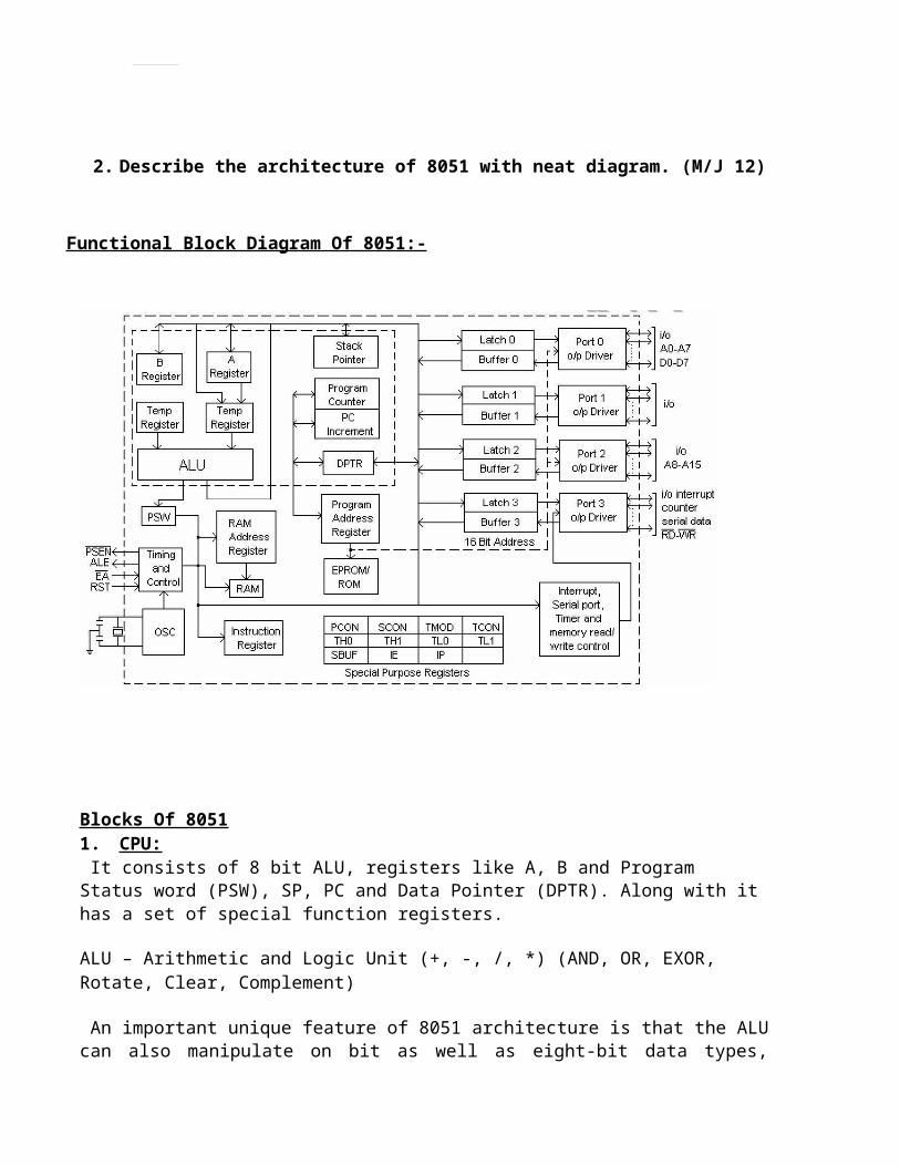
Key D7 D6 D5 D4 D3 D2 D1 D0K1 1 1 1 1 1 1 1 0K2 1 1 1 1 1 1 0 1K3 1 1 1 1 1 0 1 1K4 1 1 1 1 0 1 1 1K5 1 1 1 0 1 1 1 1K6 1 1 0 1 1 1 1 1K7 1 0 1 1 1 1 1 1K8 0 1 1 1 1 1 1 1
4.How do you interface a 4X4 matrix keyboard using 8051 microcontroller. (N/D’11)
Matrix Keyboard Interfacing:-Matrix keyboard connections is to reduce the number of connections. Here 16 keys are
arranged in 4 rows and 4 columns. This matrix keyboard requires 8 lines to make all connections instead of the 16 lines required. If the keys are connected individually, the matrix key board may require 2 ports –an input &an output port. When any key is pressed it starts corresponding row & column. When the key is identified by data sent on the output port & input port received from the input port.
Port1 (P1)
output portPort2 (P2)
Input port
Rows Logic 0(0V)
No key is pressed
Columns
Logic 1(5V)
No key is pressed

LOOK UP TABLE:-ORG 2000HKcode 0: 0,1,2,3Kcode1 : 4,5,6,7Kcode2 : 8,9,A,BKcode3 : C,D,E,F
PROGRAM:-MOV P2, FFH Configure P2 as input portK3: MOV P1, #00H
Ground all rows
K1: MOV A, P2
Read columnsANL A, #0FH
Masking
CJNE A, #0FH, K1ACALL delay
Debouncing time
K2: MOV A, P2ANL A, #0FHCJNE A, #0FH, OverSJMP K2Over: ACALL delay
wait for bouncing delay
MOV A, P2
Read columns
ANL A, #0FH
MaskingCJNE A, #0FH Over1SJMP K2Over1: MOV P1, #FEH
Ground row0
MOV A, P2ANL A, #0FHCJNE A, #0FH, Row0
MOV P1, #FDH
Ground Row1
MOV A, P2ANL A, #0FCJNE A, #0FH, Row1MOV P1, #FBHGround Row2MOV A, P2ANL A, #0FHCJNE A, #0FH, Row2MOV P1, #F7HGround Row3MOV A, P2ANL A, #0FHCJNE A, #0FH, Row3SJMP K3Row 0: MOV DPTR, #Kcode0

SJMP FindRow1: MOV DPTR, #Kcode1SJMP FindRow2: MOV DPTR, #Kcode2SJMP FindRow3: MOV DPTR, #Kcode3SJMP FindFind: RRC AJNC MatchIf cy = 0 go to matchINC DPTRSJMP FindMatch: CLR AMOVC A,@A+DPTRMOV DPTR, #3000HMOVX @DPTR, ASJMP K3
5.Write short notes on LCD interface. [May-2009]
Display Interfacing:- Usually datas are displayed using LED, LCD&CRT displays. For displaying large &small amount of datas we use CRT&LED or LCD respectively. Here
we analyze 7 segment LED&LCD interfacing.
Interfacing 7 Segment Led Displays:-Here multiplexed 8 digit 7 segment LED display is connected in 8051 system using the
port1&port3.In this circuit port1 provides the segment data inputs to the display and port3 provides to selecting a display position at a time for multiplexing the displays. Here transistors are used to drive the LED segments. We have to send the proper 7segment code of a particular digit that is to be displayed on the port1
PROGRAM:-MOV R0, #07MOV R1, #7FMOV DPTR, #6000HMOV P3, R1a: MOVX A, @DPTR MOV P1, AMOV A, R1INC DPTR RR A MOV P3, A MOV

R1, A DJNZ R0, ab: SJMP b
INTERFACING LCD DISPLAY:-
Liquid crystals are the materials that have the properties of liquid as well as solid crystal. The term liquid crystal refers to the fact that these compounds have a crystalline arrangement of molecules, yet they flow like a liquid .According to the operation, LCD may be classified as two types
1) Field effect type2) Dynamic scattering type


IC 4543 B is a BCD to 7 segments latch/decoder/driver. There are 3 control terminals which are used to control IC 4543B.These are
LD
Latch Disable
HIGHPH
Phase
60HZ square wave
BL
Blank
LOWThe display can be blanked by simply driving the Blank (BL) terminal of the logic HIGH state.
If LD=1BCD inputs are decoded &fed to 7segment displayIf LD=1BCD inputs are Latched in to memory &fed to 7segment
6.Explain with a program to rotate the stepper motor in both clockwise and anticlockwise direction using 8051 microcontroller. (N/D’11)
Stepper Motor InterfacingA stepper motor is a digital motor. It can be driven by digital signal. Figure shows the
typical two phase motor interfaced using port 1 of 8051. Motor shown in the circuit has two phases, with centre tap winding. The center taps of these windings are connected to the 12V supply. Due to this, motor can be excited by grounding four terminals of the two windings. Motor can be rotated in steps by giving proper excitation sequence to these windings. The lower nibble of port 1 of the 8051 is used to generate excitation signals in the proper sequence.
We know that the stepper motor is stepped from one position to the next by changing the currents through the fields in the motor. The winding inductance opposes the change in current and this puts limit on the stepping rate. For higher stepping rates and more torque, it is necessary to use a higher voltage source and current limiting resistors as shown in figure. By adding series resistance, we decrease L/R time constant, which allows the current to change more rapidly in the windings. There is a power loss across series resistor, but designer has to compromise between power and speed.

PROGRAM:-
AGAIN:
BACK:
ETC:MOV R0 # COUNTMOC DPTR, #ETCMOV R1, #04MOVX A, @DPTRMOV P1, ALCALL DELAYINC DPTRDJNZ R1, BACKDJNZ R0, AGAINRETORG 3000HDB 03H, 06H, 09H, 0CH
