wet processing techniques for achieving ultra … sematech 2joel barnett outline • cmos scaling...
TRANSCRIPT
Accelerating the next technology revolution
Copyright ©2010Advanced Materials Research Center, AMRC, International SEMATECH Manufacturing Initiative, and ISMI are servicemarks of SEMATECH, Inc. SEMATECH, and the SEMATECH logo are registered servicemarks of SEMATECH, Inc. All other servicemarks and trademarks are the property of their respective owners.
Wet Processing Techniques for Achieving Ultra-shallow Junctions in Future CMOS Devices
Joel Barnett, Richard Hill, Chris Hobbs and Prashant Majhi07-October-2010
07-October-2010 SEMATECH 2Joel Barnett
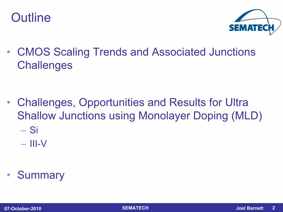
Outline
• CMOS Scaling Trends and Associated Junctions Challenges
• Challenges, Opportunities and Results for Ultra Shallow Junctions using Monolayer Doping (MLD)– Si– III-V
• Summary

07-October-2010 SEMATECH 3Joel Barnett
How Is the Industry Changing?Consumers Demand Low Power with High Performance , Mobile Devices
07-October-2010 SEMATECH 4Joel Barnett
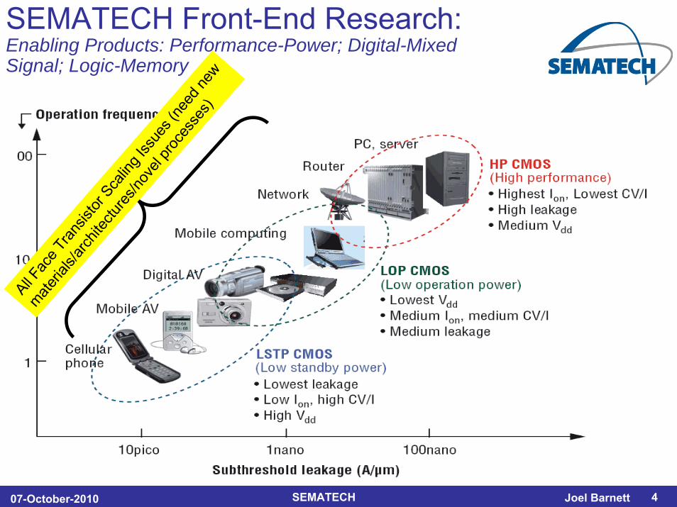
SEMATECH Front-End Research: Enabling Products: Performance-Power; Digital-Mixed Signal; Logic-Memory
All Fac
e Tra
nsist
or S
calin
g Iss
ues (
need
new
materia
ls/ar
chite
cture
s/nov
el pr
oces
ses)
07-October-2010 SEMATECH 5Joel Barnett
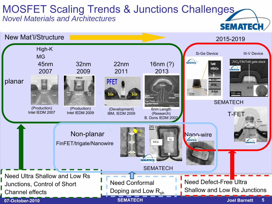
MOSFET Scaling Trends & Junctions Challenges Novel Materials and Architectures
Key InnovationsKey Innovations
New Mat’l/StructureHigh-K MG
FinFET/trigate/Nanowire
45nm2007
(Production))Intel IEDM 2009 Intel IEDM 2009
32nm2009
22nm2011
(Development)IBM, IEDM 2009
16nm (?)2013
planar
Non-planar
6nm Length(Research)
B. Doris IEDM 2002
2015-2019
III-V Device
SEMATECH
SEMATECH(Production))
Intel IEDM 2007 Intel IEDM 2007
Si-Ge Device
T-FET
Nano-wire
10 nm10 nm
15.5 nm
16.4 nm
17.9 nm
42.6 nm
HardMaskSi3N4SiO2
Need Conformal Doping and Low Rsh
Need Defect-Free Ultra Shallow and Low Rs JunctionsNeed Defect-Free Ultra Shallow and Low Rs Junctions
Need Ultra Shallow and Low RsJunctions, Control of Short Channel effects

07-October-2010 SEMATECH 6Joel Barnett
III-V: Enabling High Performance AND Low Power
Power (a.u.)
Lower Power
Higher Performance
07-October-2010 SEMATECH 7Joel Barnett
MLD Goal
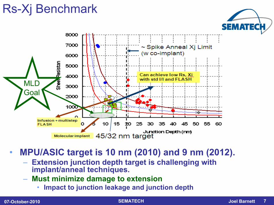
Rs-Xj Benchmark
• MPU/ASIC target is 10 nm (2010) and 9 nm (2012).– Extension junction depth target is challenging with
implant/anneal techniques. – Must minimize damage to extension
• Impact to junction leakage and junction depth

07-October-2010 SEMATECH 8Joel Barnett
MLD and Silicon
07-October-2010 SEMATECH 9Joel Barnett
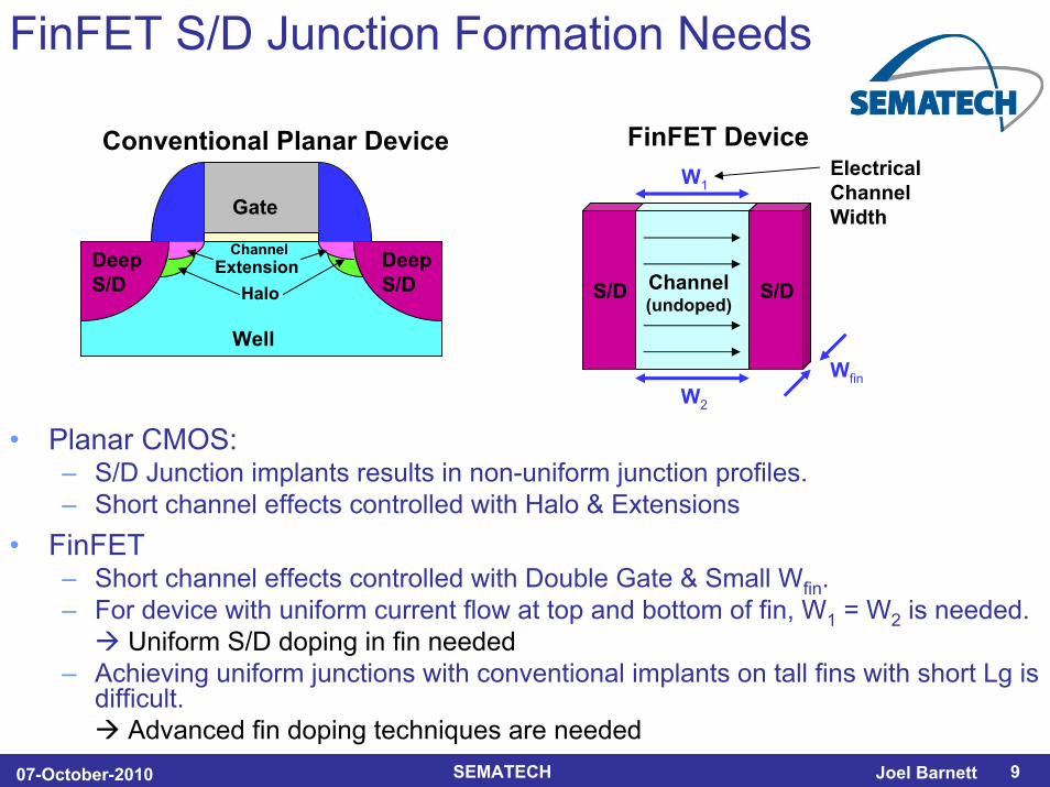
FinFET S/D Junction Formation Needs
• Planar CMOS:– S/D Junction implants results in non-uniform junction profiles.– Short channel effects controlled with Halo & Extensions
• FinFET– Short channel effects controlled with Double Gate & Small Wfin.– For device with uniform current flow at top and bottom of fin, W1 = W2 is needed.
Uniform S/D doping in fin needed– Achieving uniform junctions with conventional implants on tall fins with short Lg is
difficult.Advanced fin doping techniques are needed
Gate
Well
DeepS/D
DeepS/D
ExtensionHalo
Channel
Conventional Planar Device FinFET Device
S/D S/DChannel(undoped)
W1
W2
Wfin
ElectricalChannelWidth
07-October-2010 SEMATECH 10Joel Barnett
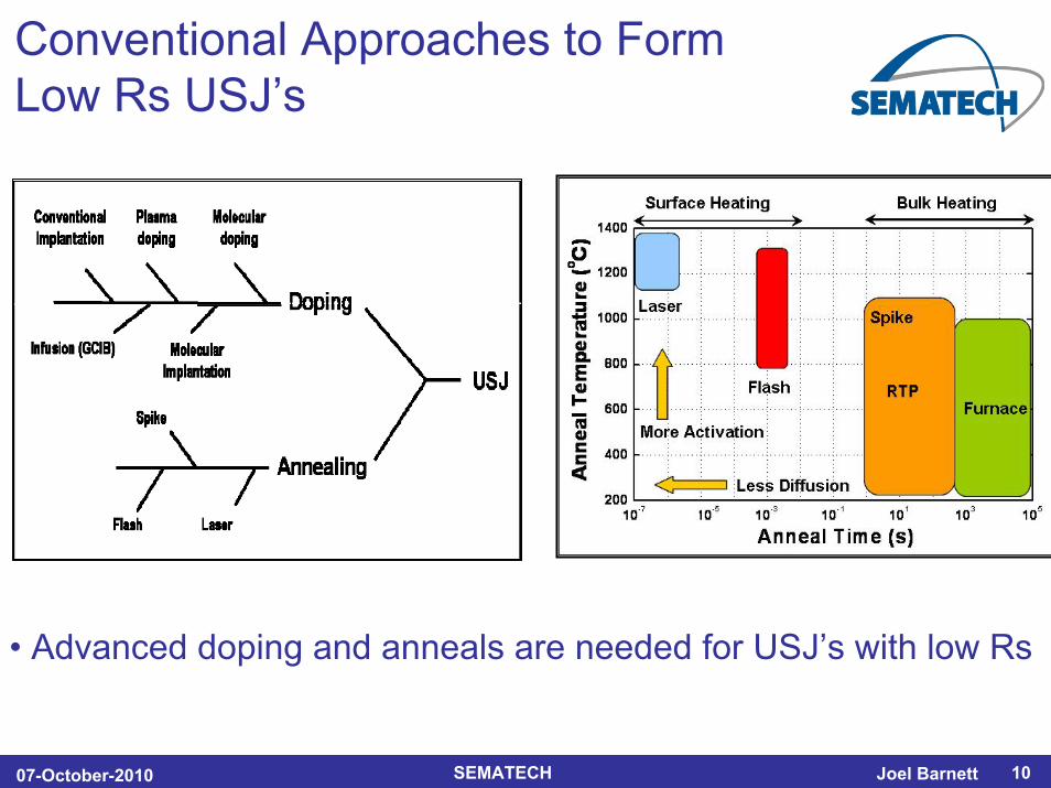
Conventional Approaches to Form Low Rs USJ’s
• Advanced doping and anneals are needed for USJ’s with low Rs
07-October-2010 SEMATECH 11Joel Barnett
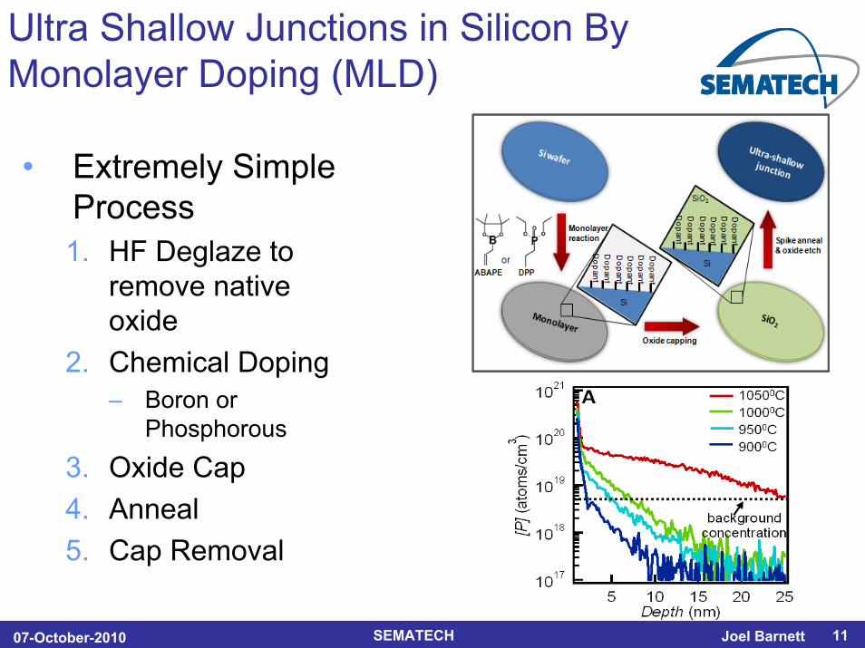
Ultra Shallow Junctions in Silicon By Monolayer Doping (MLD)
• Extremely Simple Process1. HF Deglaze to
remove native oxide
2. Chemical Doping– Boron or
Phosphorous
3. Oxide Cap4. Anneal5. Cap Removal

07-October-2010 SEMATECH 12Joel Barnett
Benefits of Monolayer Doping
• Sub 10-nm junctions achievable
• No implant damage to substrate– Very significant to LSTP and III-V as it is defect-free – Hence USJ with very low junction leakage
• Best known method for doping non-planar structures
• Minimal material loss associated with post implant clean-up
• Lower equipment and processing costs
• Applicable to various substrates (Si, SiGe, Ge, III-V)
• Long roadmap envisioned for MLD
07-October-2010 SEMATECH 13Joel Barnett
UC Berkeley MLD Process for Si Substrates
• Si wafers are treated with dilute hydrofluoric acid to remove the native SiO2.
• The Si surface is then reacted with dopants and mesitylene as a solvent for 2.5 h at 120°C to assemble a dopant-containing monolayer.
• SiO2 is electron-beam evaporated as a cap
• The substrate is spike annealed between 900-1050°C in Ar ambient to drive in the atoms and achieve USJs.
http://nano.eecs.berkeley.edu/publications/MLD_NatureMat_2008.pdf
07-October-2010 SEMATECH 14Joel Barnett
MLD of Si: Manufacturing Issues to Address
• Mesitylene solvent Process: 2.5 hours @ 120°C• Mesitylene Boiling Point (BP) is 140°C / Flash Point
(FP) is 44°C– University work carried out in a glove box with a dry N2
environment, and all reactions performed under argon bubbling to ensure an oxygen-free environment
• Semiconductor industry disinclined to run potentially explosive process– Major equipment manufacturers have declined running
demonstrations with Mesitylene
• Will require integration to properly implement masks to differentiate n and p junctions– Typical photoresist mask will not hold up to solvents– Can incorporate oxide mask as part of oxide cap process
http://nano.eecs.berkeley.edu/publications/MLD_NatureMat_2008.pdf
07-October-2010 SEMATECH 15Joel Barnett
SEMATECH Plans/Progress for USJ of Si
• Reengineer process to be safer– Raise solvent FP– Lower Process Temperature
• Requirements for alternative solvent – Aromatic– Small molecular structure– No ligand exchange during reaction
• Requirement for reaction process– Process Temp Process Time
07-October-2010 SEMATECH 16Joel Barnett
1E+17
1E+18
1E+19
1E+20
1E+21
0 5 10 15 20 25 30Depth (nm)
P C
once
ntra
tion
(ato
ms/
cm3 )
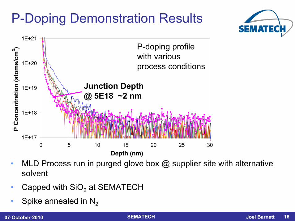
• MLD Process run in purged glove box @ supplier site with alternative solvent
• Capped with SiO2 at SEMATECH
• Spike annealed in N2
P-Doping Demonstration Results
Junction Depth @ 5E18 ~2 nm
P-doping profile with various process conditions
07-October-2010 SEMATECH 17Joel Barnett
MLD and III-V
07-October-2010 SEMATECH 18Joel Barnett
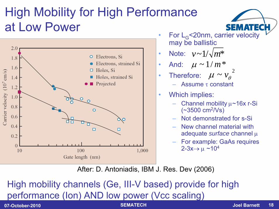
After: D. Antoniadis, IBM J. Res. Dev (2006)
• For LG<20nm, carrier velocity may be ballistic
• Note:• And:• Therefore:
– Assume τ constant
• Which implies:– Channel mobility μ~16x r-Si
(~3500 cm2/Vs) – Not demonstrated for s-Si– New channel material with
adequate surface channel μ– For example: GaAs requires
2-3x→ μ ~104
~1/ *v m*/1~ mμ
2~ θμ v
High Mobility for High Performance at Low Power
High mobility channels (Ge, III-V based) provide for high performance (Ion) AND low power (Vcc scaling)
07-October-2010 SEMATECH 19Joel Barnett
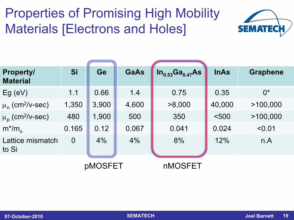
Property/Material
Si Ge GaAs In0.53Ga0.47As InAs Graphene
Eg (eV) 1.1 0.66 1.4 0.75 0.35 0*μn (cm2/v-sec) 1,350 3,900 4,600 >8,000 40,000 >100,000μp (cm2/v-sec) 480 1,900 500 350 <500 >100,000m*/mo 0.165 0.12 0.067 0.041 0.024 <0.01Lattice mismatch to Si
0 4% 4% 8% 12% n.A
Properties of Promising High Mobility Materials [Electrons and Holes]
pMOSFET nMOSFET
07-October-2010 SEMATECH 20Joel Barnett
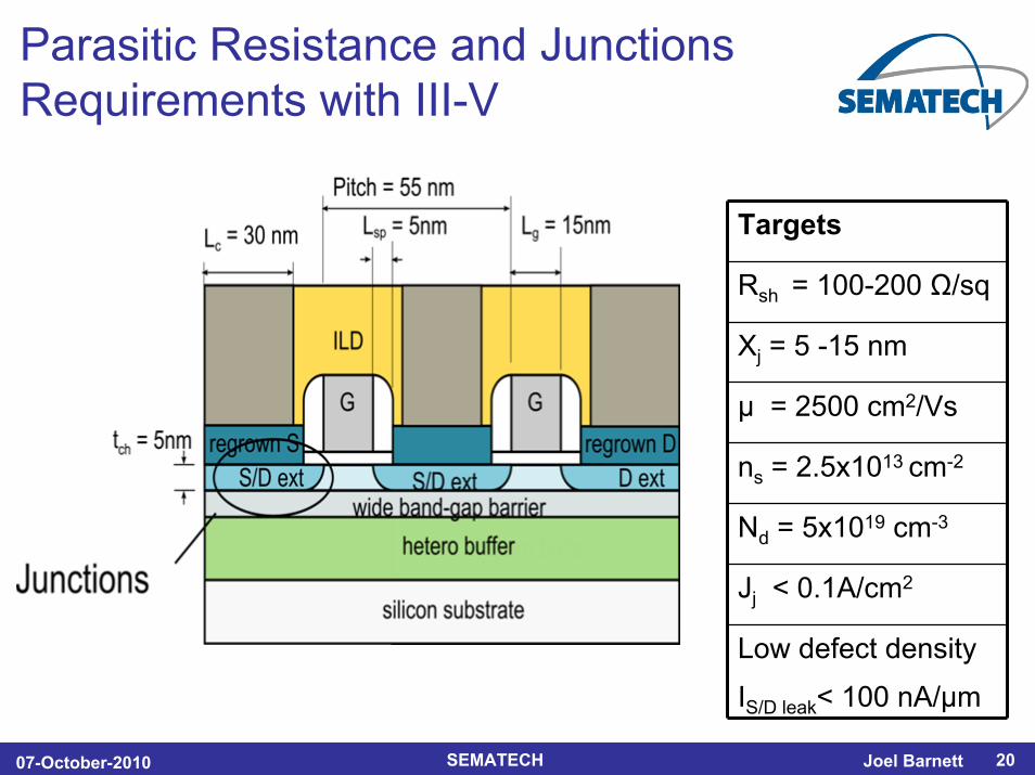
Targets
Rsh = 100-200 Ω/sq
Xj = 5 -15 nm
µ = 2500 cm2/Vs
ns = 2.5x1013 cm-2
Nd = 5x1019 cm-3
Jj < 0.1A/cm2
Low defect density
IS/D leak< 100 nA/µm
Parasitic Resistance and Junctions Requirements with III-V
07-October-2010 SEMATECH 21Joel Barnett
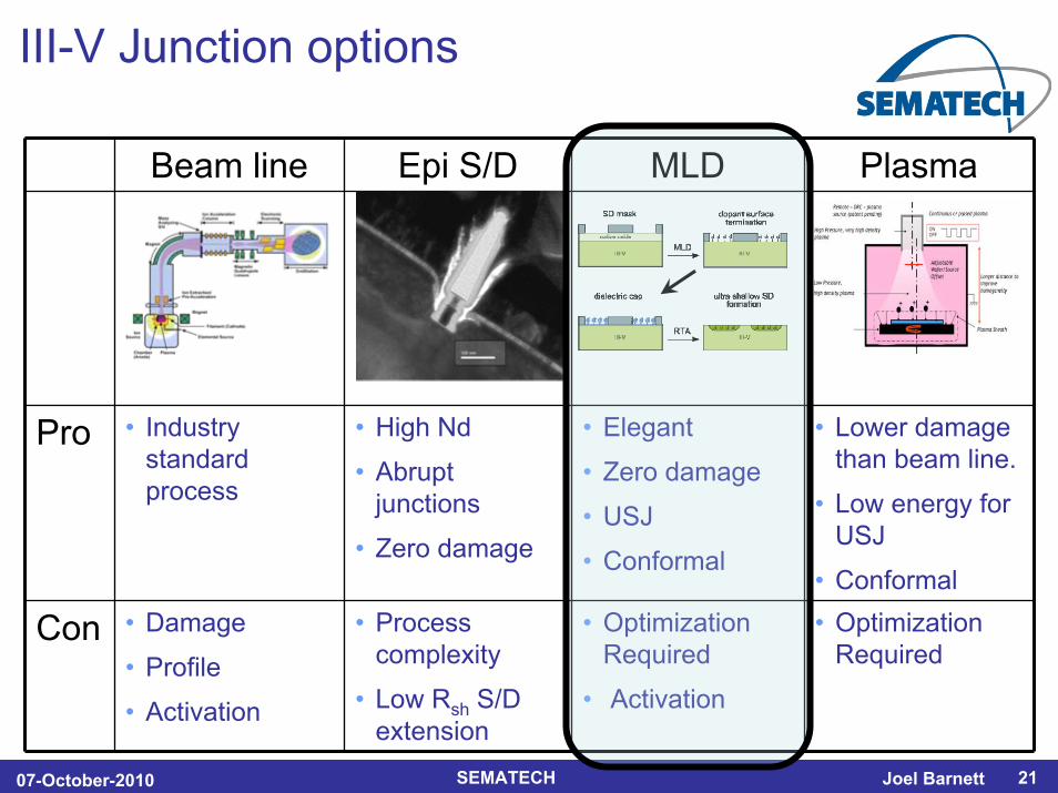
Beam line Epi S/D MLD Plasma
Pro • Industry standard process
• High Nd
• Abrupt junctions
• Zero damage
• Elegant
• Zero damage
• USJ
• Conformal
• Lower damage than beam line.
• Low energy for USJ
• Conformal
Con • Damage
• Profile
• Activation
• Process complexity
• Low Rsh S/D extension
• Optimization Required
• Activation
• Optimization Required
III-V Junction options

07-October-2010 SEMATECH 22Joel Barnett
Challenges with III-V USJ Implant/Anneal Options
• Damage in the crystal lattice– Leakage of low power transistors
• Accurate placement of dopant profile– Currently devices use spike anneals to activate dopant,
but unlikely to meet the targets for future generations.
• Accurate placement of dopant due to angle– Shrinking wells and device isolation
• Cost– Expensive tools, process complexity
07-October-2010 SEMATECH 23Joel Barnett
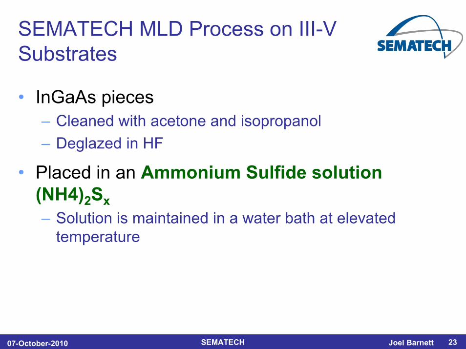
SEMATECH MLD Process on III-V Substrates
• InGaAs pieces – Cleaned with acetone and isopropanol– Deglazed in HF
• Placed in an Ammonium Sulfide solution(NH4)2Sx– Solution is maintained in a water bath at elevated
temperature

07-October-2010 SEMATECH 24Joel Barnett
How does S Passivation Work?
• Two competitive chemical reaction processes occuring– GaAs + S2- GaS + As2S3 sulfides– Ga + As sulfides + H2O GaxOy + AsxOy
• Second reaction is stronger– Sulfide layer formed is mostly converted into oxides– Oxides are soluble in water.
• One monolayer of S atoms remains on the surface
• The atomic surface density is 5.6Ex14 /cm2, which represents the maximum areal sulfur dose– Assuming a perfect monolayer
Li J. Appl Phys, 78 (4) 2764 (1995)
07-October-2010 SEMATECH 25Joel Barnett
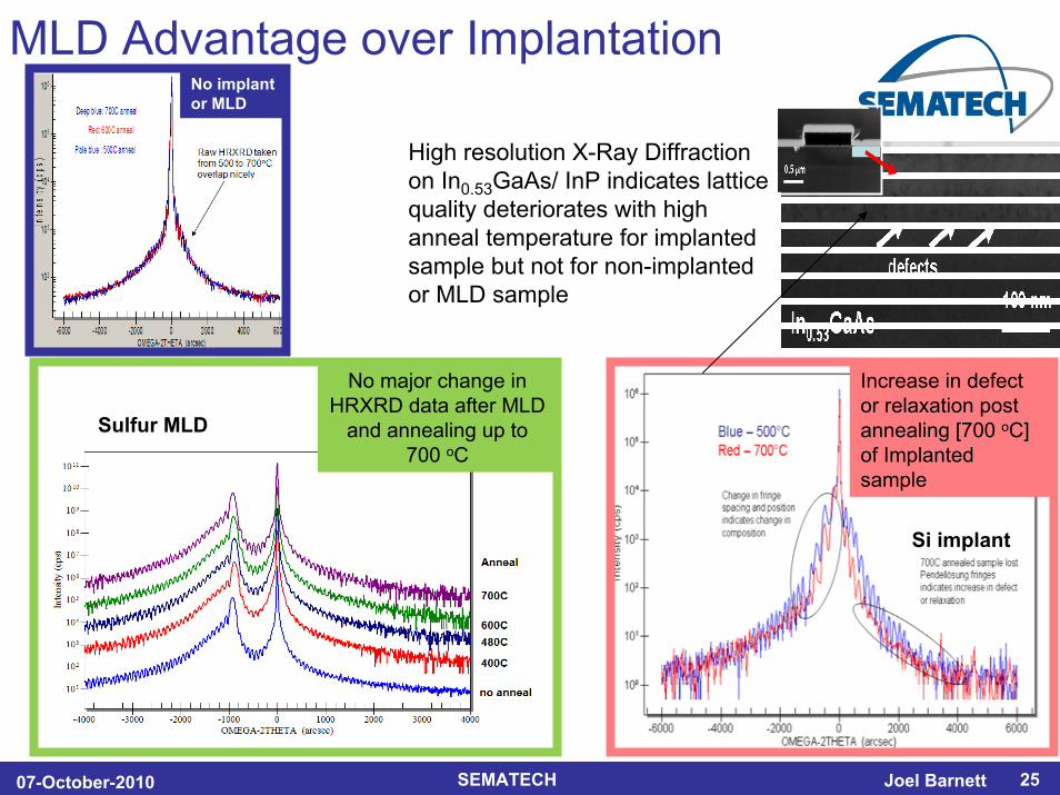
MLD Advantage over Implantation
No major change in HRXRD data after MLD
and annealing up to 700 oC
Increase in defect or relaxation post annealing [700 oC] of Implanted sample
High resolution X-Ray Diffraction on In0.53GaAs/ InP indicates lattice quality deteriorates with high anneal temperature for implanted sample but not for non-implanted or MLD sample
Si implant
Sulfur MLD
No implant or MLD
07-October-2010 SEMATECH 26Joel Barnett
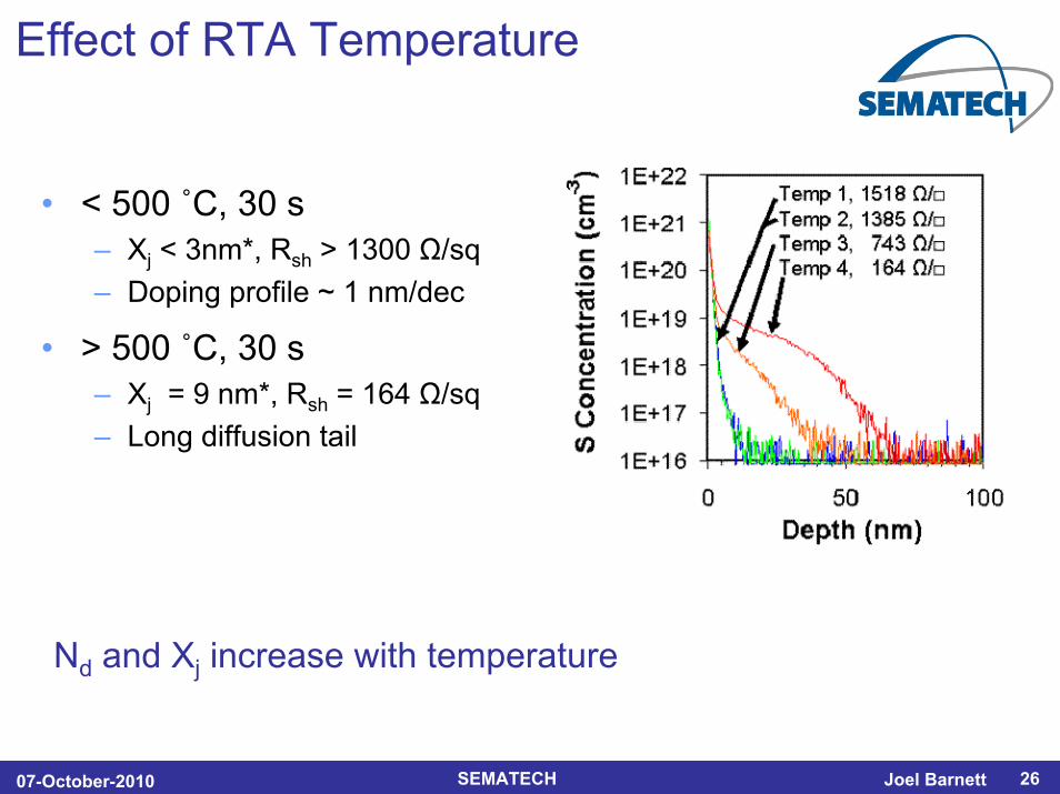
Effect of RTA Temperature
• < 500 ˚C, 30 s– Xj < 3nm*, Rsh > 1300 Ω/sq– Doping profile ~ 1 nm/dec
• > 500 ˚C, 30 s – Xj = 9 nm*, Rsh = 164 Ω/sq– Long diffusion tail
Nd and Xj increase with temperature

07-October-2010 SEMATECH 27Joel Barnett
1E+16
1E+17
1E+18
1E+19
1E+20
1E+21
1E+22
0 50 100 150
Depth (nm)
S C
onc.
(ato
ms/
cm3)
RTA, 30s, 164 Ω/
T1, ms, 450 Ω/
T2, ms, 277 Ω/
Effect of ms-Flash Anneal
Ms-flash has higher near surface concentration, but not increased activation, further optimization necessary.
Sample Rsh* µ* n*
Ω/sq cm2/Vs x1012 cm-2
Temp1 450 3200 4.3
Temp2 277 1460 15
RTA, 30s 164 2682 14
* VdP Hall data. ** Estimated TpTi
Tp
timete
mp.
Ms- flash profile
07-October-2010 SEMATECH 28Joel Barnett
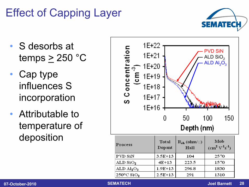
― PVD SiN― ALD SiO2― ALD Al2O3
Effect of Capping Layer
• S desorbs at temps > 250 °C
• Cap type influences S incorporation
• Attributable to temperature of deposition
07-October-2010 SEMATECH 29Joel Barnett
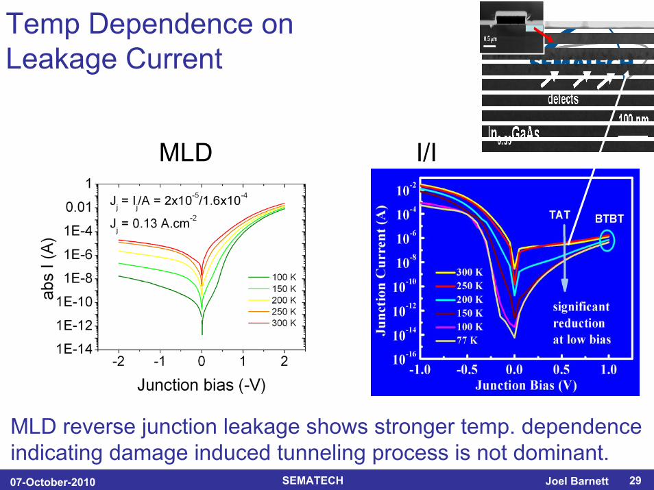
Temp Dependence on Leakage Current
MLD reverse junction leakage shows stronger temp. dependence indicating damage induced tunneling process is not dominant.
MLD I/I
07-October-2010 SEMATECH 30Joel Barnett
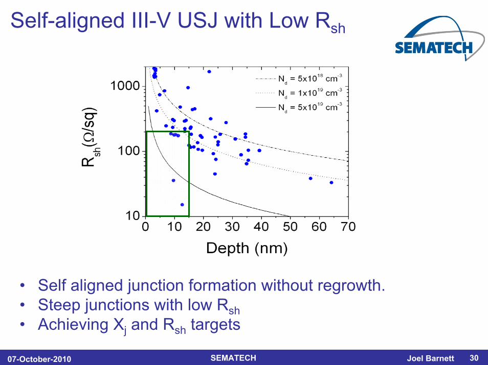
Self-aligned III-V USJ with Low Rsh
• Self aligned junction formation without regrowth. • Steep junctions with low Rsh• Achieving Xj and Rsh targets
07-October-2010 SEMATECH 31Joel Barnett
0
1000
2000
3000
4000
5000
6000
7000
8000
0 5 10 15 20 25 30 35 40 45 50 55 60 65 70 75
Junction Depth (nm)
Shee
t Res
istanc
e (Ω/sq.)
Old Data
0
1000
2000
3000
4000
5000
6000
7000
8000
0 5 10 15 20 25 30 35 40 45 50 55 60 65 70 75
Junction Depth (nm)
Shee
t Res
istanc
e (Ω/sq.)
0
1000
2000
3000
4000
5000
6000
7000
8000
0 5 10 15 20 25 30 35 40 45 50 55 60 65 70 75
Junction Depth (nm)
Shee
t Res
ista
nce
Flash
Spike Anneal Xj Limit
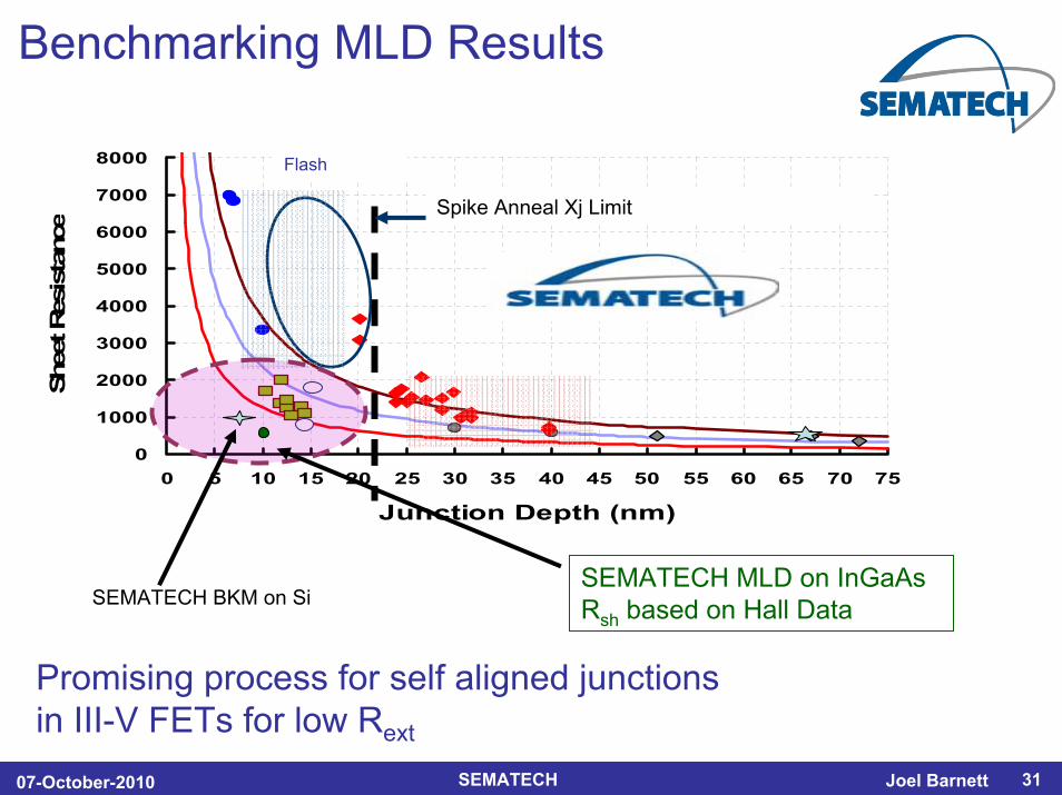
Benchmarking MLD Results
SEMATECH BKM on SiSEMATECH MLD on InGaAsRsh based on Hall Data
Promising process for self aligned junctions in III-V FETs for low Rext
07-October-2010 SEMATECH 32Joel Barnett
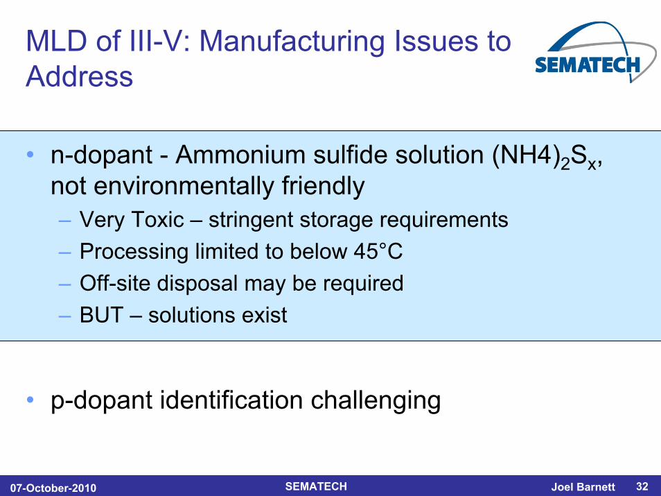
MLD of III-V: Manufacturing Issues to Address
• n-dopant - Ammonium sulfide solution (NH4)2Sx, not environmentally friendly– Very Toxic – stringent storage requirements– Processing limited to below 45°C– Off-site disposal may be required– BUT – solutions exist
• p-dopant identification challenging
07-October-2010 SEMATECH 33Joel Barnett
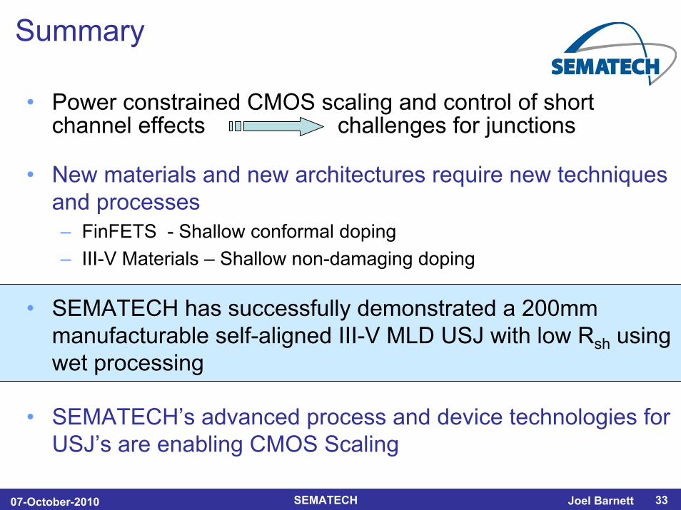
Summary
• Power constrained CMOS scaling and control of short channel effects challenges for junctions
• New materials and new architectures require new techniques and processes– FinFETS - Shallow conformal doping– III-V Materials – Shallow non-damaging doping
• SEMATECH has successfully demonstrated a 200mm manufacturable self-aligned III-V MLD USJ with low Rsh using wet processing
• SEMATECH’s advanced process and device technologies for USJ’s are enabling CMOS Scaling
07-October-2010 SEMATECH 34Joel Barnett
Worldwide collaborationSEMATECH and ISMI members