who gets the highest salary? - the hebrew uaph.huji.ac.il/courses/2014_15/83842/2.pdf · who gets...
TRANSCRIPT

1
2
3
Who gets the highest salary
1 Semiconductor device engineer
2 Algorithm engineer
3 Optical design engineer
4 Mechanical engineer
5 None of the above - Powerpoint engineer
4
Your host today
Mike Adel
5
Agenda
A few industry semilog plots
Computational lithography
Example 1 - OPC
Example 2 - SMO
Computational metrology
Simulation of the interaction of light with periodic structures
Example 1 ndash OCD (drill down)
Optical overlay metrology
6
What is a TLA
Hint 1 - it is autological
Hint 2 - previous slide contained four
Three Letter Acronym
7
Source Semiconductor Industry Association
The Semiconductor Market Era of the Consumer
0
10
20
30
40
50
60
70
80
90
100
19
60
19
65
19
70
19
75
19
80
19
85
19
90
19
95
20
00
20
05
20
10
Govt Corporate Consumer
Semiconductor Demand by Segment Faster Smaller Cheaper
semiconductor semilog plots
9
1
10
100
1000
10000
100000
1970 1980 1990 2000 2010 2020
days t
o 1
0 m
illi
on
so
ld
Days to 10 million sold
era of the corporationhellip hellipera of the consumer
10
The dollars are also on a semilog plot
11
ldquoRrdquo = k1(λNA)
ldquoRrdquo λ
k1
12
Features shrink on a semilog plot
13
Number of transistors are on a semilog plat
14
01
1
10
J-00 J-01 J-02 J-03 J-04 J-05 J-06 J-07 J-08 J-09 J-10 J-11 J-12 J-13
Year
TM
U (
nm
) Immersion
EUV
TPL
Dry ArF
KrF
Archer 200s
Archer 10
Archer 10XT
Archer AIM
Archer AIM+
Archer 100Archer 200i
DPL
Archer 300
Swordfish
Archer 400
Mobius
OMD Moorersquos Law update ndash straightening the discontinuity
01 02 03 04 05 06 07 08 09 10 11 12 13
Year
01
1
10
Imaging sensor
Scatterometry sensor
Sbs matching [nm] 015
Precision [nm] 015
TIS3sigma [nm] 015
TMU [nm] 026
- Logic OVL TMU requirements
- DRAM OVL TMU requirements
- Flash OVL TMU requirements
- - Archer OVL TMU
15
What is a lithography tool
OPC ndash Optical Proximity Correction
17
18 Date of download 11232014 Copyright copy 2014 SPIE All rights reserved
Wavefront-based pixel inversion algorithm for generation of subresolution assist features
Jue-Chin Yu Peichen Yu Hsueh-Yung Chao
[+] Author Affiliations
J MicroNanolith MEMS MOEMS 10(4) 043014 (December 01 2011)doi10111713663249
History Received March 29 2011 Revised October 04 2011 Accepted November 022011 Published December 01 2011
J MicroNanolith MEMS MOEMS 201110(4)043014-043014-12 doi10111713663249
OPC is ldquoinverse lithographyrdquo
SMO ndash Source Mask Optimization
20
The steps of SMO
21
SMO relies on ldquoco-optimizationrdquo
Copyright copy 2010 KLA-Tencor Corporation wwwkla-tencorcom Date of download 11232014 Copyright copy 2014 SPIE All rights reserved
Description and example of a standard parametric and freeform source type These are the illumination choices for optimization in
ASML BRION Tachyon SMO
From Experimental verification of source-mask optimization and freeform illumination for
22-nm node static random access memory cells J MicroNanolith MEMS MOEMS 201110(1)013008-013008-10 doi10111713541778
23
Like all good simulation based methods the
process is cyclic
OCD ndash Optical Critical Dimension metrology
25
26
Fig 1 Citation
Daesuk Kim Hyunsuk Kim Robert Magnusson Yong Jai Cho Won Chegal Hyun Mo Cho Snapshot phase sensitive scatterometry based on double-channel spectral carrier frequency concept Opt Express 19 23790-23799 (2011)
httpwwwopticsinfobaseorgoeabstractcfmuri=oe-19-24-23790
Image copy2011 Optical Society of America and may be used for noncommercial purposes only Report a copyright concern regarding this image
27
Optical simulation methods - RCWA
The electric fields can be obtained from Maxwellrsquos equations by using the boundary conditions of the
grating region In this grating region (0 lt z lt d) the periodic dielectric function is expandable with a
Fourier series having a period L as
ε(x)=sumhεhexp(j2πhLx)
(1)
where εh is the h-th Fourier component of the dielectric function in the grating region
For the TE mode the electric field in region I and II can be represented as follows [8]
EIy=Eincy+sumiRiexp[minusj(kxixminuskIziz)]EIIy=sumiTiexpminusj[kxix+kIIzi(zminusd)]
(2)
Here Eincy is the incident normalized electric field and kxi is determined from the Floquet [1] condition and
is given by
kxi=k0[nIsinθminusi(λ0L)]
(3)
where
klzi=⎧⎩⎨k0[nl2minus(kxik0)2]12thinspthinspthinspthinspthinspthinspthinspthinspk0nlgtkximinusjk0[(kxik0)minusnl2]thinspthinspthinspthinspthinspthinspthinspthinspthinspthinspkxigtk0nlthinspthinspthinspthinspthinspthinspthinspthinspthinspthinspthinspthinspthinspthinspthinspthinspthinspthinspthinspthinspthinspthinspthinspthinspthinspthinspthinspthinspthinspthinspthinspthinspthinspthinspthinspthinspthinspthinspthinspthinspthinspthinspthinspthinspthinspthinspthinspthinspthinspthinspthinspthinspthinspthinspthinspthinspthinsp
thinspthinspthinspthinspthinspthinspthinspthinspthinspthinspthinspthinspthinspthinspthinspthinspthinspthinspthinspthinspthinspthinspthinspthinspthinspthinspthinspthinspl=III
[1] httpwwwengrukyedu~gedneycoursesee625NotesPeriodicStructurespdf
28
Rigorous coupled wave analysis cont
By applying Maxwellrsquos equations in the grating region and matching the boundary conditions at the interfaces of the three regions one can determine the unknown amplitudes Ri and Ti of the diffracted
waves In the specular spectroscopic scatterometry only the 0th
order (when i=0) diffracted reflectance
coefficientR0 is used [2] and the R0 corresponds to RTE in Eq (5) for the TE mode Likewise we can
obtain RTM by using the 0th
order diffracted reflectance coefficient for the TM mode Here note that the two reflection coefficients RTE and RTM are related to the two ellipsometric parameters Ψ and Δ as
ρ=RpRs=RTERTM=∣∣∣RTERTM∣∣∣ei(δTEminusδTM)=tanΨeiΔ
(5) where δTE and δTM represent the phase shifts of the TE and TM modes respectively The term tanΨ can
be obtained from the amplitude ratio value between the TE and the TM mode Also the phase difference
Δ between the TE and TM mode can be obtained by subtracting δTM from δTE
29
FinFET fabrication ndash challenging geometric models
30
31
BACKGROUND OF THE INVENTION
For a number of industrial applications it is useful to determine the surface metrology of samples such as
thickness of thin films their refractive indices and the profile parameters of surface features such as grating on
semiconductor wafers A number of metrology tools are now available for performing optical measurements on
semiconductors Such tools can include scatterometers such as spectroscopic reflectometers angle-
resolved reflectometers and angle-resolved ellipsometers and spectroscopic ellipsometers Such
scatterometry techniques have been extensively used in semiconductor metrology eg for measuring film
thickness
In doing scatterometry it is common to look at light reflected from a periodic line or three dimensional
structures A theoretical spectrum for scattered light may be calculated based on a theoretical model based on
assumptions about the geometry and material nature of the structure and knowledge of physics and optics
This theoretical spectrum may be compared against a measured spectrum obtained through scatterometry
measurements Through an iterative regression the theoretical spectrum may be varied by varying the
assumptions about the geometry and material nature of the structure until the theoretical spectrum matches
the measured spectrum In an alternative implementation the measured spectrum may be compared to a pre-
computed set of theoretical spectra The theoretical spectrum that most closely matches the measured
spectrum may be reported or it may be used as the initial theoretical spectrum to start interactive regression
Another implementation interpolation between the pre-calculated theoretical spectra may be used to
determine an interpolated theoretical spectrum that most closely matches the measured spectrum The shape
model that corresponds to the theoretical spectrum that most closely matches the measured spectrum is then
said to be the shape model that most closely represents the actual shape of the structure that produced the
measured spectrum However in order to properly model the theoretical spectrum it is important to have an
accurate model of the optical system used to obtain the measurements The properties include the azimuth
angle φ which may be the angle of the plane of incidence of the probe beam with respect to some reference
direction in the plane of the sample such as the direction of the lines of a grating target
32
The inverse problem solved by regression
33
or by libraries
Break time
Optical overlay metrology
36
36
Differential scatterometry overlay metrology
0th order scatterometry 1st order scatterometry
S0 S+1 S-1
D = S0(cell 2) - S0(cell 1) D = S+1(cell 1) ndash S-1(cell 1)
Differential signal Differential signal
JBischoff et al Proc SPIE 4344 (2001) pp 222-233
CP Ausschnitt Proc SPIE 5375 (2004) pp 51-65
J Petit et al Proc SPIE 5752 (2005) pp 420-428
W Yang et al Proc SPIE 5038 (2003) pp 200-207
H T Huang et al Proc SPIE 5038 (2003) pp 126-137
Pupil image
of diff signals = of cells -1 of diff signals = of cells
37
Evolution has generated diversity in pupil structure
38
The pupil means many things
Exposure vs Depth of field
39
What happens when we put the image sensor in
the pupil
40 40 confidential
Field imaging architecture
Illumination
Field
Stop
Fiber from
source
Image Sensor
Objective
Target
BS
Mirror
pupil
41 41 confidential
Pupil imaging architecture
IFS
Fiber from
source
CFS
Pupil image Sensor
Objective
Target
BS
Apodizer (spatial filter)
Mirror
Apodizer (spatial filter)
42
42
Overlay metrology is enabled by quantification
of symmetry breaking Field imaging Pupil imaging
S0 S+1 S-1
Pupil image
-F0 F0
Rotational Symmetry Translational Symmetry
43
Itrsquos all about diffraction
θ d
dSinθ = m λ
44
For zero offset first orders are symmetric
I+
I_
I0
Ax1 = I_- I+
X1
X2 Y2
Y1
45
Summary
The pupil has many meanings and uses in optics
The pupil is also a location in the optical path which
enables the image to be viewed in the Fourier domain
Overlay metrology is enabled by pupil imaging of overlaid
periodic structures
Translational offsets between periodic structures are
required in order to quantify symmetry breaking in the pupil
image
-F0 F0 I+
I_
I0

10
The dollars are also on a semilog plot
11
ldquoRrdquo = k1(λNA)
ldquoRrdquo λ
k1
12
Features shrink on a semilog plot
13
Number of transistors are on a semilog plat
14
01
1
10
J-00 J-01 J-02 J-03 J-04 J-05 J-06 J-07 J-08 J-09 J-10 J-11 J-12 J-13
Year
TM
U (
nm
) Immersion
EUV
TPL
Dry ArF
KrF
Archer 200s
Archer 10
Archer 10XT
Archer AIM
Archer AIM+
Archer 100Archer 200i
DPL
Archer 300
Swordfish
Archer 400
Mobius
OMD Moorersquos Law update ndash straightening the discontinuity
01 02 03 04 05 06 07 08 09 10 11 12 13
Year
01
1
10
Imaging sensor
Scatterometry sensor
Sbs matching [nm] 015
Precision [nm] 015
TIS3sigma [nm] 015
TMU [nm] 026
- Logic OVL TMU requirements
- DRAM OVL TMU requirements
- Flash OVL TMU requirements
- - Archer OVL TMU
15
What is a lithography tool
OPC ndash Optical Proximity Correction
17
18 Date of download 11232014 Copyright copy 2014 SPIE All rights reserved
Wavefront-based pixel inversion algorithm for generation of subresolution assist features
Jue-Chin Yu Peichen Yu Hsueh-Yung Chao
[+] Author Affiliations
J MicroNanolith MEMS MOEMS 10(4) 043014 (December 01 2011)doi10111713663249
History Received March 29 2011 Revised October 04 2011 Accepted November 022011 Published December 01 2011
J MicroNanolith MEMS MOEMS 201110(4)043014-043014-12 doi10111713663249
OPC is ldquoinverse lithographyrdquo
SMO ndash Source Mask Optimization
20
The steps of SMO
21
SMO relies on ldquoco-optimizationrdquo
Copyright copy 2010 KLA-Tencor Corporation wwwkla-tencorcom Date of download 11232014 Copyright copy 2014 SPIE All rights reserved
Description and example of a standard parametric and freeform source type These are the illumination choices for optimization in
ASML BRION Tachyon SMO
From Experimental verification of source-mask optimization and freeform illumination for
22-nm node static random access memory cells J MicroNanolith MEMS MOEMS 201110(1)013008-013008-10 doi10111713541778
23
Like all good simulation based methods the
process is cyclic
OCD ndash Optical Critical Dimension metrology
25
26
Fig 1 Citation
Daesuk Kim Hyunsuk Kim Robert Magnusson Yong Jai Cho Won Chegal Hyun Mo Cho Snapshot phase sensitive scatterometry based on double-channel spectral carrier frequency concept Opt Express 19 23790-23799 (2011)
httpwwwopticsinfobaseorgoeabstractcfmuri=oe-19-24-23790
Image copy2011 Optical Society of America and may be used for noncommercial purposes only Report a copyright concern regarding this image
27
Optical simulation methods - RCWA
The electric fields can be obtained from Maxwellrsquos equations by using the boundary conditions of the
grating region In this grating region (0 lt z lt d) the periodic dielectric function is expandable with a
Fourier series having a period L as
ε(x)=sumhεhexp(j2πhLx)
(1)
where εh is the h-th Fourier component of the dielectric function in the grating region
For the TE mode the electric field in region I and II can be represented as follows [8]
EIy=Eincy+sumiRiexp[minusj(kxixminuskIziz)]EIIy=sumiTiexpminusj[kxix+kIIzi(zminusd)]
(2)
Here Eincy is the incident normalized electric field and kxi is determined from the Floquet [1] condition and
is given by
kxi=k0[nIsinθminusi(λ0L)]
(3)
where
klzi=⎧⎩⎨k0[nl2minus(kxik0)2]12thinspthinspthinspthinspthinspthinspthinspthinspk0nlgtkximinusjk0[(kxik0)minusnl2]thinspthinspthinspthinspthinspthinspthinspthinspthinspthinspkxigtk0nlthinspthinspthinspthinspthinspthinspthinspthinspthinspthinspthinspthinspthinspthinspthinspthinspthinspthinspthinspthinspthinspthinspthinspthinspthinspthinspthinspthinspthinspthinspthinspthinspthinspthinspthinspthinspthinspthinspthinspthinspthinspthinspthinspthinspthinspthinspthinspthinspthinspthinspthinspthinspthinspthinspthinspthinspthinsp
thinspthinspthinspthinspthinspthinspthinspthinspthinspthinspthinspthinspthinspthinspthinspthinspthinspthinspthinspthinspthinspthinspthinspthinspthinspthinspthinspthinspl=III
[1] httpwwwengrukyedu~gedneycoursesee625NotesPeriodicStructurespdf
28
Rigorous coupled wave analysis cont
By applying Maxwellrsquos equations in the grating region and matching the boundary conditions at the interfaces of the three regions one can determine the unknown amplitudes Ri and Ti of the diffracted
waves In the specular spectroscopic scatterometry only the 0th
order (when i=0) diffracted reflectance
coefficientR0 is used [2] and the R0 corresponds to RTE in Eq (5) for the TE mode Likewise we can
obtain RTM by using the 0th
order diffracted reflectance coefficient for the TM mode Here note that the two reflection coefficients RTE and RTM are related to the two ellipsometric parameters Ψ and Δ as
ρ=RpRs=RTERTM=∣∣∣RTERTM∣∣∣ei(δTEminusδTM)=tanΨeiΔ
(5) where δTE and δTM represent the phase shifts of the TE and TM modes respectively The term tanΨ can
be obtained from the amplitude ratio value between the TE and the TM mode Also the phase difference
Δ between the TE and TM mode can be obtained by subtracting δTM from δTE
29
FinFET fabrication ndash challenging geometric models
30
31
BACKGROUND OF THE INVENTION
For a number of industrial applications it is useful to determine the surface metrology of samples such as
thickness of thin films their refractive indices and the profile parameters of surface features such as grating on
semiconductor wafers A number of metrology tools are now available for performing optical measurements on
semiconductors Such tools can include scatterometers such as spectroscopic reflectometers angle-
resolved reflectometers and angle-resolved ellipsometers and spectroscopic ellipsometers Such
scatterometry techniques have been extensively used in semiconductor metrology eg for measuring film
thickness
In doing scatterometry it is common to look at light reflected from a periodic line or three dimensional
structures A theoretical spectrum for scattered light may be calculated based on a theoretical model based on
assumptions about the geometry and material nature of the structure and knowledge of physics and optics
This theoretical spectrum may be compared against a measured spectrum obtained through scatterometry
measurements Through an iterative regression the theoretical spectrum may be varied by varying the
assumptions about the geometry and material nature of the structure until the theoretical spectrum matches
the measured spectrum In an alternative implementation the measured spectrum may be compared to a pre-
computed set of theoretical spectra The theoretical spectrum that most closely matches the measured
spectrum may be reported or it may be used as the initial theoretical spectrum to start interactive regression
Another implementation interpolation between the pre-calculated theoretical spectra may be used to
determine an interpolated theoretical spectrum that most closely matches the measured spectrum The shape
model that corresponds to the theoretical spectrum that most closely matches the measured spectrum is then
said to be the shape model that most closely represents the actual shape of the structure that produced the
measured spectrum However in order to properly model the theoretical spectrum it is important to have an
accurate model of the optical system used to obtain the measurements The properties include the azimuth
angle φ which may be the angle of the plane of incidence of the probe beam with respect to some reference
direction in the plane of the sample such as the direction of the lines of a grating target
32
The inverse problem solved by regression
33
or by libraries
Break time
Optical overlay metrology
36
36
Differential scatterometry overlay metrology
0th order scatterometry 1st order scatterometry
S0 S+1 S-1
D = S0(cell 2) - S0(cell 1) D = S+1(cell 1) ndash S-1(cell 1)
Differential signal Differential signal
JBischoff et al Proc SPIE 4344 (2001) pp 222-233
CP Ausschnitt Proc SPIE 5375 (2004) pp 51-65
J Petit et al Proc SPIE 5752 (2005) pp 420-428
W Yang et al Proc SPIE 5038 (2003) pp 200-207
H T Huang et al Proc SPIE 5038 (2003) pp 126-137
Pupil image
of diff signals = of cells -1 of diff signals = of cells
37
Evolution has generated diversity in pupil structure
38
The pupil means many things
Exposure vs Depth of field
39
What happens when we put the image sensor in
the pupil
40 40 confidential
Field imaging architecture
Illumination
Field
Stop
Fiber from
source
Image Sensor
Objective
Target
BS
Mirror
pupil
41 41 confidential
Pupil imaging architecture
IFS
Fiber from
source
CFS
Pupil image Sensor
Objective
Target
BS
Apodizer (spatial filter)
Mirror
Apodizer (spatial filter)
42
42
Overlay metrology is enabled by quantification
of symmetry breaking Field imaging Pupil imaging
S0 S+1 S-1
Pupil image
-F0 F0
Rotational Symmetry Translational Symmetry
43
Itrsquos all about diffraction
θ d
dSinθ = m λ
44
For zero offset first orders are symmetric
I+
I_
I0
Ax1 = I_- I+
X1
X2 Y2
Y1
45
Summary
The pupil has many meanings and uses in optics
The pupil is also a location in the optical path which
enables the image to be viewed in the Fourier domain
Overlay metrology is enabled by pupil imaging of overlaid
periodic structures
Translational offsets between periodic structures are
required in order to quantify symmetry breaking in the pupil
image
-F0 F0 I+
I_
I0
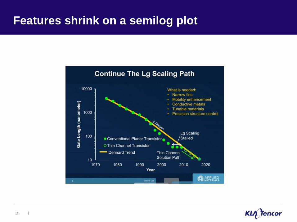
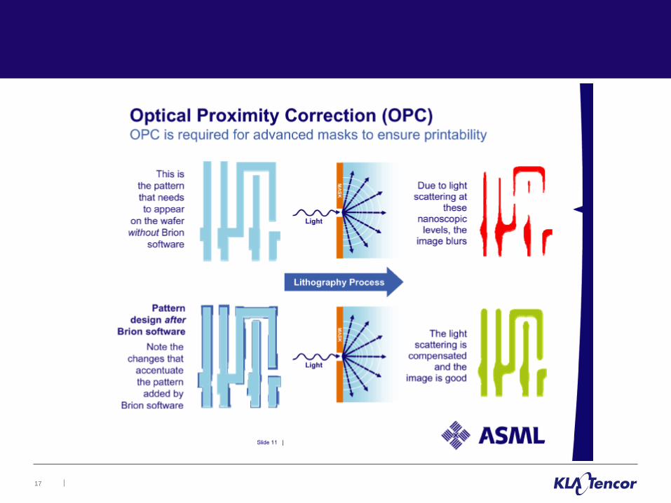
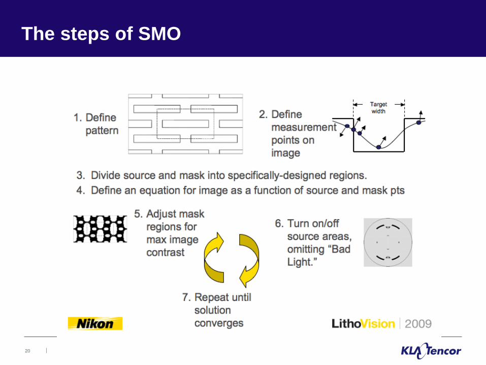
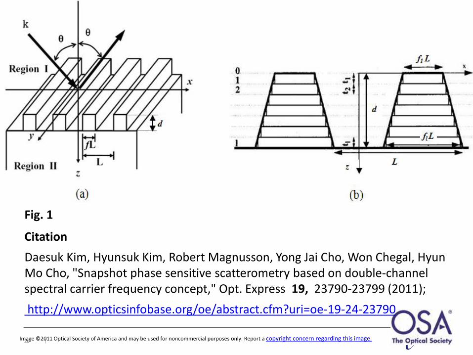
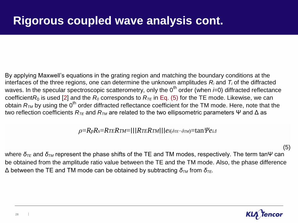

36
36
Differential scatterometry overlay metrology
0th order scatterometry 1st order scatterometry
S0 S+1 S-1
D = S0(cell 2) - S0(cell 1) D = S+1(cell 1) ndash S-1(cell 1)
Differential signal Differential signal
JBischoff et al Proc SPIE 4344 (2001) pp 222-233
CP Ausschnitt Proc SPIE 5375 (2004) pp 51-65
J Petit et al Proc SPIE 5752 (2005) pp 420-428
W Yang et al Proc SPIE 5038 (2003) pp 200-207
H T Huang et al Proc SPIE 5038 (2003) pp 126-137
Pupil image
of diff signals = of cells -1 of diff signals = of cells
37
Evolution has generated diversity in pupil structure
38
The pupil means many things
Exposure vs Depth of field
39
What happens when we put the image sensor in
the pupil
40 40 confidential
Field imaging architecture
Illumination
Field
Stop
Fiber from
source
Image Sensor
Objective
Target
BS
Mirror
pupil
41 41 confidential
Pupil imaging architecture
IFS
Fiber from
source
CFS
Pupil image Sensor
Objective
Target
BS
Apodizer (spatial filter)
Mirror
Apodizer (spatial filter)
42
42
Overlay metrology is enabled by quantification
of symmetry breaking Field imaging Pupil imaging
S0 S+1 S-1
Pupil image
-F0 F0
Rotational Symmetry Translational Symmetry
43
Itrsquos all about diffraction
θ d
dSinθ = m λ
44
For zero offset first orders are symmetric
I+
I_
I0
Ax1 = I_- I+
X1
X2 Y2
Y1
45
Summary
The pupil has many meanings and uses in optics
The pupil is also a location in the optical path which
enables the image to be viewed in the Fourier domain
Overlay metrology is enabled by pupil imaging of overlaid
periodic structures
Translational offsets between periodic structures are
required in order to quantify symmetry breaking in the pupil
image
-F0 F0 I+
I_
I0
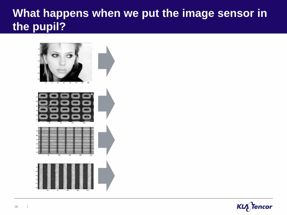
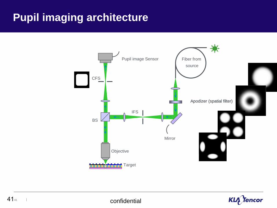
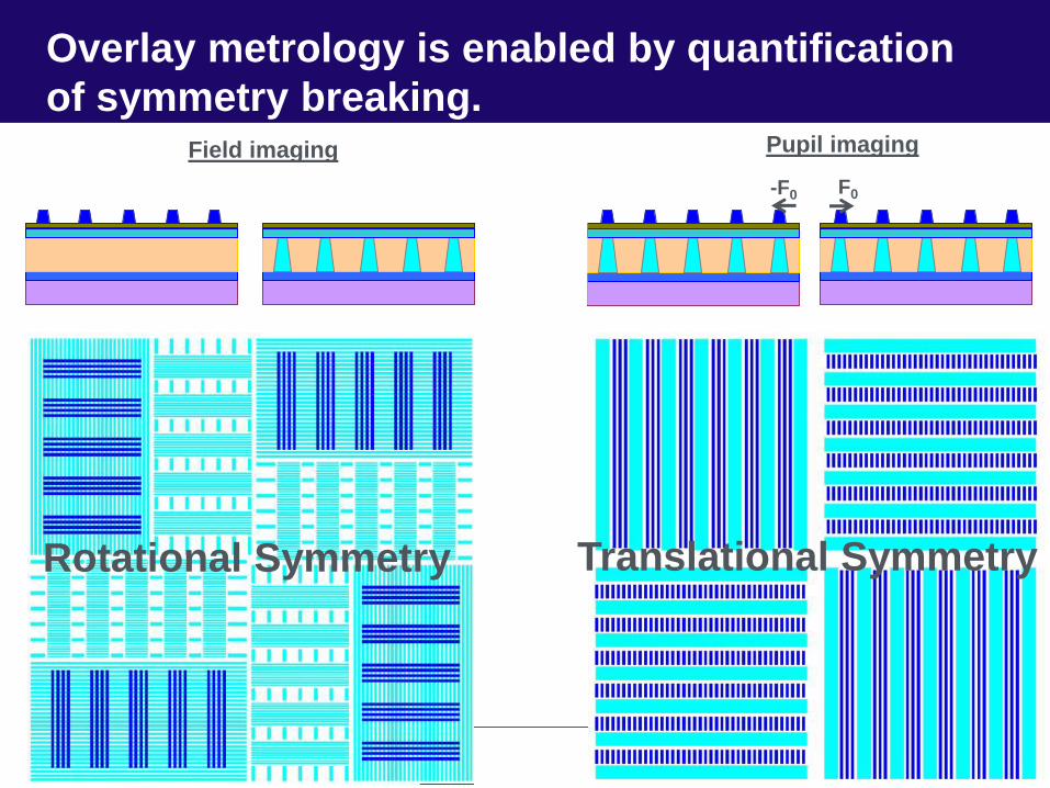
42
42
Overlay metrology is enabled by quantification
of symmetry breaking Field imaging Pupil imaging
S0 S+1 S-1
Pupil image
-F0 F0
Rotational Symmetry Translational Symmetry
43
Itrsquos all about diffraction
θ d
dSinθ = m λ
44
For zero offset first orders are symmetric
I+
I_
I0
Ax1 = I_- I+
X1
X2 Y2
Y1
45
Summary
The pupil has many meanings and uses in optics
The pupil is also a location in the optical path which
enables the image to be viewed in the Fourier domain
Overlay metrology is enabled by pupil imaging of overlaid
periodic structures
Translational offsets between periodic structures are
required in order to quantify symmetry breaking in the pupil
image
-F0 F0 I+
I_
I0
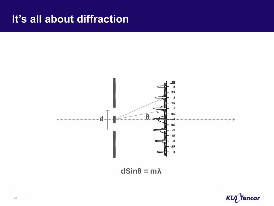