994 ieee transactions on computer-aided … · digital object identifier 10.1109/tcad.2012.2185930...
TRANSCRIPT

994 IEEE TRANSACTIONS ON COMPUTER-AIDED DESIGN OF INTEGRATED CIRCUITS AND SYSTEMS, VOL. 31, NO. 7, JULY 2012
NVSim: A Circuit-Level Performance, Energy, andArea Model for Emerging Nonvolatile Memory
Xiangyu Dong, Member, IEEE, Cong Xu, Student Member, IEEE, Yuan Xie, Senior Member, IEEE, andNorman P. Jouppi, Fellow, IEEE
Abstract—Various new nonvolatile memory (NVM) technolo-gies have emerged recently. Among all the investigated new NVMcandidate technologies, spin-torque-transfer memory (STT-RAM,or MRAM), phase-change random-access memory (PCRAM),and resistive random-access memory (ReRAM) are regarded asthe most promising candidates. As the ultimate goal of this NVMresearch is to deploy them into multiple levels in the memory hi-erarchy, it is necessary to explore the wide NVM design space andfind the proper implementation at different memory hierarchylevels from highly latency-optimized caches to highly density-optimized secondary storage. While abundant tools are availableas SRAM/DRAM design assistants, similar tools for NVM designsare currently missing. Thus, in this paper, we develop NVSim,a circuit-level model for NVM performance, energy, and areaestimation, which supports various NVM technologies, includingSTT-RAM, PCRAM, ReRAM, and legacy NAND Flash. NVSim issuccessfully validated against industrial NVM prototypes, and itis expected to help boost architecture-level NVM-related studies.
Index Terms—Analytical circuit model, MRAM, NANDFlash, nonvolatile memory, phase-change random-accessmemory (PCRAM), resistive random-access memory (ReRAM),spin-torque-transfer memory (STT-RAM).
I. Introduction
UNIVERSAL MEMORY that provides fast randomaccess, high storage density, and nonvolatility within one
memory technology becomes possible thanks to the emergenceof various new nonvolatile memory (NVM) technologies, suchas spin-torque-transfer random-access memory (STT-RAM,or MRAM), phase-change random-access memory (PCRAM),and resistive random-access memory (ReRAM). As theultimate goal of this NVM research is to devise a universalmemory that could work across multiple layers of the memoryhierarchy, each of these emerging NVM technologies has tosupply a wide design space that covers a spectrum from highly
Manuscript received March 17, 2011; revised June 22, 2011, September 26,2011, and December 16, 2011; accepted January 22, 2012. Date of currentversion June 20, 2012. This work was supported in part by the SemiconductorResearch Corporation Grant, in part by the National Science Foundation,under Grants 1147388 and 0903432, and in part by the DoE, under AwardDE-SC0005026. This paper was recommended by Associate Editor S. Mitra.
X. Dong is with Qualcomm, Inc., San Diego, CA 92121 USA (e-mail:[email protected]).
C. Xu and Y. Xie are with the Department of Computer Science andEngineering, Pennsylvania State University, University Park, PA 16802 USA(e-mail: [email protected]; [email protected]).
N. P. Jouppi is with the Intelligent Infrastructure Laboratory, Hewlett-Packard Labs, Palo Alto, CA 94304 USA (e-mail: [email protected]).
Color versions of one or more of the figures in this paper are availableonline at http://ieeexplore.ieee.org.
Digital Object Identifier 10.1109/TCAD.2012.2185930
latency-optimized microprocessor caches to highly density-optimized secondary storage. Therefore, specialized peripheralcircuitry is required for each optimization target. However,since few of these NVM technologies are mature so far, onlya limited number of prototype chips have been demonstratedand just cover a small portion of the entire design space.In order to facilitate the architecture-level NVM research byestimating the NVM performance, energy, and area valuesunder different design specifications before fabricating a realchip, in this paper, we build NVSim,1 a circuit-level modelfor NVM performance, energy, and area estimations, whichsupports various NVM technologies, including STT-RAM,PCRAM, ReRAM, and legacy NAND Flash.
The main goals of developing NVSim tool are as follows.
1) Estimate the access time, access energy, and silicon areaof NVM chips with a given organization and specificdesign options before the effort of actual fabrications.
2) Explore the NVM chip design space to find the opti-mized chip organization and design options that achievebest performance, energy, or area.
3) Find the optimal NVM chip organization and designoptions that are optimized for one design metric whilekeeping other metrics under constraints.
We build NVSim by using the same empirical modelingmethodology as CACTI [1], [2], but starting from a newframework and adding specific features for NVM technologies.Compared to CACTI, the framework of NVSim includes thefollowing new features.
1) It allows us to move sense amplifiers from inner memorysubarrays to the outer bank level and factor them out toachieve overall area efficiency of the memory module.
2) It provides more flexible array organizations and dataactivation modes by considering any combinations ofmemory data allocation and address distribution.
3) It models various types of data sensing schemes insteadof voltage-sensing scheme only.
4) It allows memory banks to be formed in a bus-likemanner rather than the H-tree manner only.
5) It provides multiple design options of buffers instead oflatency-optimized option that uses logical effort.
6) It models the cross-point memory cells rather than MOS-accessed memory cells only.
1Latest NVsim binary file release and related documentations are availableat our wiki site http://www.rioshering.com/nvsimwiki.
0278-0070/$31.00 c© 2012 IEEE

DONG et al.: NVSIM: A CIRCUIT-LEVEL PERFORMANCE, ENERGY, AND AREA MODEL 995
Fig. 1. Basic string block of NAND Flash, and the conceptual view offloating gate Flash memory cell (BL = bitline, WL = wordline, SG = selectgate).
7) It considers the subarray size limit by analyzing thecurrent sneak path.
8) It allows advanced target users to redefine memory cellproperties by providing a customization interface.
NVSim is validated against several industry prototype chipswithin the error range of 30%. In addition, we show how touse this model to facilitate the architecture-level performance,energy, and area analysis for applications that adopt theemerging NVM technologies.
II. Background of Nonvolatile Memory
In this section, we first review the technology backgroundof four types of NVMs modeled in NVSim, which are STT-RAM, PCRAM, ReRAM, and legacy NAND Flash.
A. NVM Physical Mechanisms and Write Operations
Different NVM technologies have their particular storagemechanisms and corresponding write methods.
1) NAND Flash: The physical mechanism of the Flashmemory is to store bits in the floating gate and control thegate threshold voltage. The series bit-cell string of NAND
Flash, as shown in Fig. 1(a), eliminates contacts betweenthe cells and approaches the minimum cell size of 4F 2 forlow-cost manufacturing. The small cell size, low cost, andstrong application demands make the NAND Flash dominatethe traditional nonvolatile memory market. Fig. 1(b) showsthat a Flash memory cell consists of a floating gate and acontrol gate aligned vertically. The Flash memory cell modifiesits threshold voltage VT by adding electrons to or subtractingelectrons from the isolated floating gate.
NAND Flash usually charges or discharges the floating gateby using Fowler–Nordheim tunneling or hot carrier injection.A program operation adds tunneling charges to the floatinggate and the threshold voltage becomes negative, while anerase operation subtracts charges and the threshold voltagereturns positive.
2) STT-RAM: STT-RAM uses magnetic tunnel junc-tion (MTJ) as the memory storage and leverages the differ-ence in magnetic directions to represent the memory bit. Asshown in Fig. 2, MTJ contains two ferromagnetic layers. Oneferromagnetic layer has fixed magnetization direction and itis called the reference layer, while the other layer has a freemagnetization direction that can be changed by passing a writecurrent and it is called the free layer. The relative magneti-zation direction of two ferromagnetic layers determines the
Fig. 2. Demonstration of a MRAM cell. (a) Structural view. (b) Schematicview (BL = bitline, WL = wordline, SL = sourceline).
Fig. 3. Schematic view of a PCRAM cell with a MOSFET selector transistor(BL = bitline, WL = wordline, SL = sourceline).
resistance of MTJ. If two ferromagnetic layers have the samedirections, the resistance of MTJ is low, indicating a “1” state;if two layers have different directions, the resistance of MTJis high, indicating a “0” state.
As shown in Fig. 2, when writing “0” state into STT-RAM cells (RESET operation), positive voltage differenceis established between SL and BL; when writing “1” state(SET operation), vice versa. The current amplitude requiredto reverse the direction of the free ferromagnetic layer isdetermined by the size and aspect ratio of MTJ and the writepulse duration.
3) PCRAM: PCRAM uses chalcogenide material (e.g.,GST) to store information. The chalcogenide materials canbe switched between a crystalline phase (SET state) andan amorphous phase (RESET state) with the application ofheat. The crystalline phase shows low resistivity while theamorphous phase is characterized by high resistivity. Fig. 3shows an example of a MOS-accessed PCRAM cell.
The SET operation crystallizes GST by heating it above itscrystallization temperature, and the RESET operation melt-quenches GST to make the material amorphous as illustratedin Fig. 4. The temperature is controlled by passing a specificelectrical current profile and generating the required Joule heat.High-power pulses are required for the RESET operation toheat the memory cell above the GST melting temperature. Incontrast, moderate power but longer duration pulses for theSET operation to heat the cell above the GST crystallizationtemperature but below the melting temperature [3].
4) ReRAM: Although many nonvolatile memory technolo-gies (e.g., aforementioned STT-RAM and PCRAM) are basedon electrically induced resistive switching effects, we defineReRAM as the one that involves electro and thermochemicaleffects in the resistance change of a metal/oxide/metal system.In addition, we confine our definition to bipolar ReRAM.Fig. 5 illustrates the general concept for the ReRAM workingmechanism. An ReRAM cell consists of a metal oxide layer(e.g., Ti [4], Ta [5], and Hf [6]) sandwiched by two metal(e.g., Pt [4]) electrodes. The electronic behavior of metal/oxideinterfaces depends on the oxygen vacancy concentration of themetal oxide layer. Typically, the metal/oxide interface shows

996 IEEE TRANSACTIONS ON COMPUTER-AIDED DESIGN OF INTEGRATED CIRCUITS AND SYSTEMS, VOL. 31, NO. 7, JULY 2012
Fig. 4. Temperature–time relationship during SET and RESET operations.
Fig. 5. Working mechanism of ReRAM cells.
Ohmic behavior in the case of very high doping and rectifyingin the case of low doping [4]. In Fig. 5, the TiOx region issemiinsulating indicating lower oxygen vacancy concentration,while the TiO2−x is conductive indicating higher concentration.
The oxygen vacancy in metal oxide is n-type dopant, whosedraft under the electric field can cause the change of dopingprofiles. Thus, applying electronic current can modulate theI–V curve of the ReRAM cell and further switch the cellfrom one state to the other state. Usually, for bipolar ReRAM,the cell can be switched ON (SET operation) only by applyinga negative bias and OFF (RESET operation) only by applyingthe opposite bias [4]. Several ReRAM prototypes [7]–[9] havebeen demonstrated and show promising properties on fastswitching speed and low energy consumption.
B. Read Operations
The read operations of these NVM technologies are almostthe same. Since the NVM memory cell has different resistancein ON and OFF states, the read operation can be accomplishedeither by applying a small voltage on the bitline and sensingthe current that passes through the memory cell or by injectinga small current into the bitline and sensing the voltage acrossthe memory cell. Instead of SRAM that generates complementread signals from each cell, NVM usually has a group ofdummy cells to generate the reference current or referencevoltage. The generated current (or voltage) from the to-be-readcell is then compared to the reference current (or voltage) byusing sense amplifiers. Various types of sense amplifiers aremodeled in NVSim as we discuss in Section V-B.
C. Write Endurance Issue
Write endurance is the number of times that an NVMcell can be overwritten. Among all the NVM technologiesmodeled in NVSim, only STT-RAM does not suffer from thewrite endurance issue. NAND Flash, PCRAM, and ReRAMall have limited write endurance, which is the number oftimes that a memory cell can be overwritten. NAND Flash onlyhas write endurance of 105–106. The PCRAM endurance isnow in the range between 105 and 109 [10]–[12]. ReRAMresearch currently shows endurance numbers in the range
Fig. 6. Memory array organization modeled in NVSim: a hierarchicalmemory organization includes banks, mats, and subarrays with decoders,multiplexers, sense amplifiers, and output drivers.
between 105 and 1010 [13], [14]. A projected plan by ITRS for2024 for emerging NVM, i.e., PCRAM and ReRAM, highlightendurance in the order of 1015 or more write cycles [15]. InNVSim, the write endurance limit is not modeled since NVSimis a circuit-level modeling tool.
D. Retention Time Issue
Retention time is the time that data can be retained in NVMcells. Typically, NVM technologies require retention time ofhigher than 10 years. However, in some cases, such a highretention time is not necessary. For example, Smullen et al.relaxed the retention time requirement to improve the timingand energy profile of STT-RAMs [16]. Since the tradeoffamong NVM retention time and other NVM parameters (e.g.,the duration and amplitude of write pulses) is on the devicelevel, as a circuit-level tool, NVSim does not model thistradeoff directly but instead takes different sets of NVMparameters with various retention time as the device-levelinput.
E. MOS-Accessed Structure Versus Cross-Point Structure
Some NVM technologies (e.g., PCRAM [17] andReRAM [13], [17], [18]) have the capability of building cross-point memory arrays without access devices. Conventionally,in the MOS-accessed structure, memory cell arrays are isolatedby MOS access devices and the cell size is dominated by thelarge MOS access device that is necessary to drive enoughwrite current, even though the NVM cell itself is much smaller.However, taking advantage of the cell nonlinearity, a NVMarray can be accessed without any extra access devices. Theremoval of MOS access devices leads to a memory cell size ofonly 4F 2, where F is the process feature size. Unfortunately,the cross-point structure also brings extra peripheral circuitrydesign challenges and a tradeoff among performance, energy,and area is always necessary as discussed in our previ-ous work [19]. NVSim models both the MOS-accessed andthe cross-point structures, and the modeling methodology isdescribed in the following sections.
III. NVSim Framework
The framework of NVSim is modified from CACTI [2],[20]. We add several new features, such as more flexible dataactivation modes and alternative bank organizations.
A. Device Model
NVSim uses device data from ITRS report [15] and theMASTAR tool [21] to obtain the process parameters. NVSimcovers the process nodes from 180 nm, 120 nm, 90 nm, 65 nm,45 nm, 32 nm to 22 nm and supports three transistor types,

DONG et al.: NVSIM: A CIRCUIT-LEVEL PERFORMANCE, ENERGY, AND AREA MODEL 997
which are high performance, low operating power, and lowstand-by power.
B. Array Organization
Fig. 6 shows the array organization. There are three hier-archy levels in such organization, which are bank, mat, andsubarray. Basically, the descriptions of these levels are asfollows.
1) Bank is the top-level structure modeled in NVSim. Onenonvolatile memory chip can have multiple banks. Thebank is a fully-functional memory unit, and it can beoperated independently. In each bank, multiple mats areconnected together in either H-tree or bus-like manner.
2) Mat is the building block of bank. Multiple mats in abank operate simultaneously to fulfill a memory oper-ation. Each mat consists of multiple subarrays and onepredecoder block.
3) Subarray is the elementary structure modeled in NVSim.Every subarray contains peripheral circuitry includingrow decoders, column multiplexers, and output drivers.
Conventionally, sense amplifiers are integrated on thesubarray level as modeled in CACTI [2], [20]. However, inNVSim model, sense amplifiers can be placed either on thesubarray level or on the mat level.
C. Memory Bank Type
For practical memory designs, memory cells are groupedtogether to form memory modules of different types. Forinstance:
1) the main memory is a typical RAM, which takes theaddress of data as input and returns the content of data;
2) the set-associative cache contains two separate RAMs(data array and tag array), and can return the data ifthere is a cache hit by the given set address and tag;
3) the fully-associative cache usually contains a content-addressable memory (CAM).
To cover all the possible memory designs, we model fivetypes of memory banks in NVSim: one for RAM, one forCAM, and three for set-associate caches with different accessmanners. The functionalities of these five types of memorybanks are listed as follows.
1) RAM: output the data content at the I/O interface giventhe data address.
2) CAM: output the data address at the I/O interface giventhe data content if there is a hit.
3) Cache with normal access: start to access the cache dataarray and tag array at the same time; the data contentis temporarily buffered in each mat; if there is a hit, thecache hit signal generated from the tag array is routedto the proper mats and the content of the desired cacheline is output to the I/O interface.
4) Cache with sequential access: access the cache tag arrayfirst; if there is a hit, then access the cache data arraywith the set address and the tag hit information, andfinally output the desired cache line to the I/O interface.
5) Cache with fast access: access the cache data arrayand tag array simultaneously; read the entire set content
from the mats to the I/O interface; selectively output thedesired cache line if there is a cache hit signal generatedfrom the tag array.
D. Activation Mode
We model the array organization and the data activationmodes using eight parameters, which are as follows:
1) NMR: number of rows of mat arrays in each bank;2) NMC: number of columns of mat arrays in each bank;3) NAMR: number of active rows of mat arrays during data
accessing;4) NAMC: number of active columns of mat arrays during
data accessing;5) NSR: number of rows of subarrays in each mat;6) NSC: number of columns of subarrays in each mat;7) NASR: number of active rows of subarrays during data
accessing;8) NASC: number of active columns of subarrays during
data accessing.
The values of these parameters are all constrained to be powerof two. NMR and NMC define the number of mats in a bank,and NSR and NSC define the number of subarrays in a mat.NAMR, NAMC, NASR, and NASC define the activation patterns,and they can take any values smaller than NMR, NMC, NSR,and NSC, respectively. On the contrary, the limitation of arrayorganization and data activation pattern in CACTI is causedby several constraints on these parameters such as NAMR = 1,NAMC = NMC, and NSR = NSC = NASR = NASC = 2.
NVSim has these flexible activation patterns, and is ableto model sophisticated memory accessing techniques, such assingle subarray activation [22].
E. Routing to Mats
In order to first route the data and address signals from theI/O port to the edge of memory mats and from mat to the edgesof memory subarrays, we divided all the interconnect wiresinto three categories: address wires, broadcast data wires, anddistributed data wires. Depending on the memory moduletypes and the activation modes, the initial number of wiresin each group is assigned according to the rules listed inTable I. We use the terminology block to refer to the memorywords in RAM and CAM designs and the cache lines incache designs. In Table I, Nblock is the number of blocks,Wblock is the block size, and A is the associativity in cachedesigns. The number of broadcast data wires are always keptunchanged, the number of distributed data wires is cut by halfat each routing point where data are merged, and the numberof address wires is subtracted by one at each routing pointwhere data are multiplexed.
We use the case of the cache bank with normal access todemonstrate how the wires are routed from the I/O port to theedges of the mats. For simplicity, we suppose the data arrayand the tag array are two separate modules. While the dataand the tag arrays usually have different mat organizationsin practice, we use the same 4 × 4 mat organization for thedemonstration purpose as shown in Figs. 7 and 8. The total16 mats are positioned in a 4 × 4 formation and connectedby a 4-level H-tree. Therefore, NMR and NMC are 4. As an

998 IEEE TRANSACTIONS ON COMPUTER-AIDED DESIGN OF INTEGRATED CIRCUITS AND SYSTEMS, VOL. 31, NO. 7, JULY 2012
TABLE I
Initial Number of Wires in Each Routing Group
Address Wire (NAW ) Broadcast Data Wire (NBW ) Distributed Data Wire (NDW )
RAMlog2Nblock
0 Wblock
CAM Wblock 0
Normal accessData array log2 (Nblock/A) log2A Wblock
Tag array log2 (Nblock/A) Wblock A
CacheSequential access
Data array log2Nblock 0 Wblock
Tag array log2 (Nblock/A) Wblock A
Fast accessData array log2 (Nblock/A) 0 WblockA
Tag array log2 (Nblock/A) Wblock A
Fig. 7. Example of the wire routing in a 4×4 mat organization for the dataarray of a 8-way 1 MB cache with 64 B cache lines.
Fig. 8. Example of the wire routing in a 4 × 4 mat organization for the tagarray of a 8-way 1 MB cache with 64 B cache lines.
example, we use the activation mode in which two rows andtwo columns of the mat array are activated for each dataaccess, and the activation groups are Mat {0, 2, 8, 10}, Mat{1, 3, 9, 11}, Mat {4, 6, 12, 14}, and Mat {5, 7, 13, 15}.Thereby, NAMR and NAMC are 2. In addition, we set the cacheline size (block size) to 64 B, the cache associativity to A = 8,and the cache bank capacity to 1 MB so that the number ofcache lines (blocks) is Nblock = 8M/512 = 16 384, the blocksize in the data array is Wblock,data = 512, and the block sizein the tag array is Wblock,tag = 16 (assuming 32-bit addressingand labeling dirty block with one bit).
According to Table I, the initial number of address wires(NAW ) is log2Nblock/A = 11 for both data and tag arrays.For data array, the initial number of broadcast data wires(NBW,data) is log2A = 3, which is used to transit the tag hitsignals from the tag array to the corresponding mats in the dataarray; the initial number of distributed data wires (NDW,data)is Wblock,data = 512, which is used to output the desired cacheline from the mats to the I/O port. For tag array, the broadcastdata wire (NBW,tag) is Wblock,tag = 16, which is sent from theI/O port to each of the mat in the tag array; the initial numberof distributed data wires (NDW,tag) is A = 8, which is used tocollect the tag hit signals from each mat to the I/O port andthen send to the data array after a 8-to-3 encoding process.
From the I/O port to the edges of the mats, the numbersof wires in the three categories are changed as follows anddemonstrated in Figs. 7 and 8, respectively.
1) At node A, the activated mats are distributed in both theupper and the bottom parts, so node A is a merging node.As per the routing rule, the address wires and broadcastdata wires remain the same but the distributed data wiresare cut in half. Thus, the wire segment between node Aand B have NAW = 11, NBW,data = 3, NDW,data = 256,NBW,tag = 16, and NDW,tag = 4.
2) Node B is again a merging node. Thus, the wiresegments between nodes B and C have NAW = 11,NBW,data = 3, NDW,data = 128, NBW,tag = 16, andNDW,tag = 2.
3) At node C, the activated mats are allocated only in oneside, either from Mat 0/1 or from Mat 4/5, so NodeC is a multiplexing node. As per the routing rule, thedistributed data wires and broadcast data wires remainthe same but the address wires are decremented by 1.Thus, the wire segments between nodes C and D haveNAW = 10, NBW,data = 3, NDW,data = 128, NBW,tag = 16,and NDW,tag = 2.
4) Finally, node D is another multiplexing node. Thus,the wire segments at the mat edges have NAW = 9,NBW,data = 3, NDW,data = 128, NBW,tag = 16, andNDW,tag = 2.
Thereby, each mat in the data array takes the input of a 9-bit setaddress and a 3-bit tag hit signals (which can be treated as theblock address in a 8-way associative set), and it generates theoutput of a 128-bit data. A group of four data mats providesthe desired output of a 512-bit (64 B) cache line, and foursuch groups cover the entire 11-bit set address space. On theother hand, each mat in the tag array takes the input of a9-bit set address and a 16-bit tag, and it generates 2-bit hitsignals (01 or 10 for hit and 00 for miss). A group of four tagmats concatenate their hit signals and provide the informationwhether a 16-bit tag hits in a 8-way associated cache with a9-bit address space, and four such groups extend the addressspace from 9-bit to the desired 11-bit.
Other configurations in Table I can be explained in thesimilar manner.
F. Routing to Subarrays
The interconnect wires from mat to the edges of memorysubarrays are routed using the same H-tree organization asshown in Fig. 9, and its routing strategy is the same wirepartitioning rule described in Section III-E. However, NVSim

DONG et al.: NVSIM: A CIRCUIT-LEVEL PERFORMANCE, ENERGY, AND AREA MODEL 999
Fig. 9. Example of mat using internal sensing and H-tree routing.
Fig. 10. Example of mat using external sensing and bus-like routing.
provides an option of building mat using a bus-like routingorganization as illustrated in Fig. 10. The wire partitioningrule described in Section III-E can also be applied to thebus-like organization with a few extensions. For example, amultiplexing node with a fanout of N decrements the numberof address wires by log2N instead of 1; a merging node witha fanout of N divides the number of distributed data wires byN instead of 2.
Furthermore, the default setting including sense amplifiersin each subarray can cause a dominant portion of the total arrayarea. As a result, for high-density memory module designs,NVSim provides an option of moving the sense amplifiersout of the subarray and using external sensing. In addition, abus-like routing organization is designed to associate with theexternal sensing scheme.
Fig. 9 shows a common mat using H-tree organization toconnect all the sense amplifier-included subarrays together.In contrast, the new external sensing scheme is illustratedin Fig. 10. In this external sensing scheme, all the senseamplifiers are located at the mat level and the output signalsfrom each sense amplifier-free subarray are partial-swing. Itis obvious that the external sensing scheme has much higherarea efficiency compared to its internal sensing counterpart.However, as a penalty, sophisticated global interconnect tech-nologies, such as repeater inserting, cannot be used in theexternal sensing scheme since all the global signals are partial-swing before passing through the sense amplifiers.
G. Subarray Size Limit
The subarray size is a critical parameter to design a memorymodule. Basically, smaller subarrays are preferred for latency-optimized designs since they reduce local bitline and wordlinelatencies and leave the global interconnects to be handled by
Fig. 11. Maximum subarray size versus nonlinearity and driving current.
the sophisticated H-tree solution. In contrast, larger subarraysare preferred for area-optimized designs since they can greatlyamortize the peripheral circuitry area. However, the subarraysize has its upper limit in practice.
For MOS-accessed subarrays, the leakage current pathsfrom unselected wordlines are the main constraint to the bitlinelength. For cross-point subarrays, the leakage current pathissue is much more severe as there is no MOSFET in suchsubarrays that can isolate selected and unselected cells [23].The half-select cells in cross-point subarrays serve as currentdividers in the selected row and columns, preventing thearray size from growing unbounded since the available drivingcurrent is limited. The minimum current that a column writedriver should provide is determined by
Idriver = Iwrite + (Nr − 1) × I(Vwrite/2) (1)
where Iwrite and Vwrite are the current and voltage of eitherRESET or SET operation. Nonlinearity of memory cells isreflected by the fact that the current through cross-pointmemory cells is not directly proportional to the voltage appliedon it, which means nonconstant resistance of the memory cell.In NVSim, we define a nonlinearity coefficient, Kr, to quantifythe current divider effect of the half selected memory cells asfollows:
Kr =R(Vwrite/2)
R(Vwrite)(2)
where R(Vwrite/2) and R(Vwrite) are equivalent static resistanceof cross-point memory cells biased at Vwrite/2 and Vwrite,respectively. Then, we derive the upper limit in a cross-pointsubarray size by
Nr =
(Idriver
Iwrite− 1
)× 2 × Kr + 1 (3)
Nc =
(Idriver
Iwrite− Nsc
)× 2 × Kr + Nsc (4)
where Idriver is the maximum driving current that the writedriver attached to the selected row/column can provide andNsc is the number of selected columns per row. Thus, Nr andNc are the maximum numbers of rows and columns in a cross-point subarray.
As shown in Fig. 11, the maximum cross-point subarraysize increases with larger current driving capability or largernonlinearity coefficient.
H. Two-Step Write in Cross-Point Subarrays
In cross-point structures, SET and RESET operations cannotbe performed simultaneously. Thus, two steps of write oper-
1000 IEEE TRANSACTIONS ON COMPUTER-AIDED DESIGN OF INTEGRATED CIRCUITS AND SYSTEMS, VOL. 31, NO. 7, JULY 2012
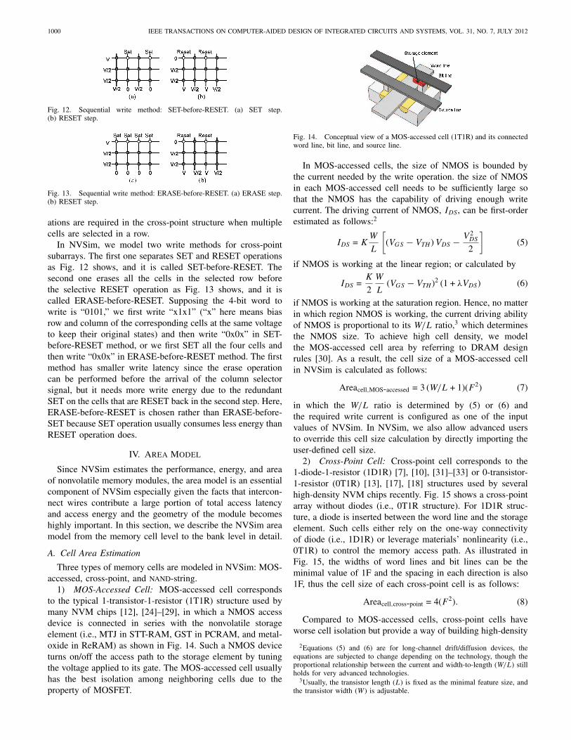
Fig. 12. Sequential write method: SET-before-RESET. (a) SET step.(b) RESET step.
Fig. 13. Sequential write method: ERASE-before-RESET. (a) ERASE step.(b) RESET step.
ations are required in the cross-point structure when multiplecells are selected in a row.
In NVSim, we model two write methods for cross-pointsubarrays. The first one separates SET and RESET operationsas Fig. 12 shows, and it is called SET-before-RESET. Thesecond one erases all the cells in the selected row beforethe selective RESET operation as Fig. 13 shows, and it iscalled ERASE-before-RESET. Supposing the 4-bit word towrite is “0101,” we first write “x1x1” (“x” here means biasrow and column of the corresponding cells at the same voltageto keep their original states) and then write “0x0x” in SET-before-RESET method, or we first SET all the four cells andthen write “0x0x” in ERASE-before-RESET method. The firstmethod has smaller write latency since the erase operationcan be performed before the arrival of the column selectorsignal, but it needs more write energy due to the redundantSET on the cells that are RESET back in the second step. Here,ERASE-before-RESET is chosen rather than ERASE-before-SET because SET operation usually consumes less energy thanRESET operation does.
IV. Area Model
Since NVSim estimates the performance, energy, and areaof nonvolatile memory modules, the area model is an essentialcomponent of NVSim especially given the facts that intercon-nect wires contribute a large portion of total access latencyand access energy and the geometry of the module becomeshighly important. In this section, we describe the NVSim areamodel from the memory cell level to the bank level in detail.
A. Cell Area Estimation
Three types of memory cells are modeled in NVSim: MOS-accessed, cross-point, and NAND-string.
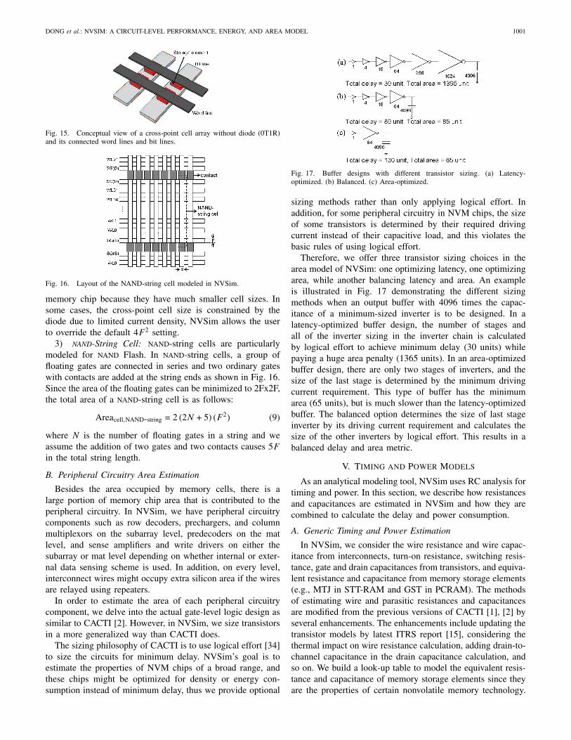
1) MOS-Accessed Cell: MOS-accessed cell correspondsto the typical 1-transistor-1-resistor (1T1R) structure used bymany NVM chips [12], [24]–[29], in which a NMOS accessdevice is connected in series with the nonvolatile storageelement (i.e., MTJ in STT-RAM, GST in PCRAM, and metal-oxide in ReRAM) as shown in Fig. 14. Such a NMOS deviceturns on/off the access path to the storage element by tuningthe voltage applied to its gate. The MOS-accessed cell usuallyhas the best isolation among neighboring cells due to theproperty of MOSFET.
Fig. 14. Conceptual view of a MOS-accessed cell (1T1R) and its connectedword line, bit line, and source line.
In MOS-accessed cells, the size of NMOS is bounded bythe current needed by the write operation. the size of NMOSin each MOS-accessed cell needs to be sufficiently large sothat the NMOS has the capability of driving enough writecurrent. The driving current of NMOS, IDS , can be first-orderestimated as follows:2
IDS = KW
L
[(VGS − VTH ) VDS − V 2
DS
2
](5)
if NMOS is working at the linear region; or calculated by
IDS =K
2
W
L(VGS − VTH )2 (1 + λVDS) (6)
if NMOS is working at the saturation region. Hence, no matterin which region NMOS is working, the current driving abilityof NMOS is proportional to its W/L ratio,3 which determinesthe NMOS size. To achieve high cell density, we modelthe MOS-accessed cell area by referring to DRAM designrules [30]. As a result, the cell size of a MOS-accessed cellin NVSim is calculated as follows:
Areacell,MOS-accessed = 3 (W/L + 1)(F 2) (7)
in which the W/L ratio is determined by (5) or (6) andthe required write current is configured as one of the inputvalues of NVSim. In NVSim, we also allow advanced usersto override this cell size calculation by directly importing theuser-defined cell size.
2) Cross-Point Cell: Cross-point cell corresponds to the1-diode-1-resistor (1D1R) [7], [10], [31]–[33] or 0-transistor-1-resistor (0T1R) [13], [17], [18] structures used by severalhigh-density NVM chips recently. Fig. 15 shows a cross-pointarray without diodes (i.e., 0T1R structure). For 1D1R struc-ture, a diode is inserted between the word line and the storageelement. Such cells either rely on the one-way connectivityof diode (i.e., 1D1R) or leverage materials’ nonlinearity (i.e.,0T1R) to control the memory access path. As illustrated inFig. 15, the widths of word lines and bit lines can be theminimal value of 1F and the spacing in each direction is also1F, thus the cell size of each cross-point cell is as follows:
Areacell,cross-point = 4(F 2). (8)
Compared to MOS-accessed cells, cross-point cells haveworse cell isolation but provide a way of building high-density
2Equations (5) and (6) are for long-channel drift/diffusion devices, theequations are subjected to change depending on the technology, though theproportional relationship between the current and width-to-length (W/L) stillholds for very advanced technologies.
3Usually, the transistor length (L) is fixed as the minimal feature size, andthe transistor width (W) is adjustable.
DONG et al.: NVSIM: A CIRCUIT-LEVEL PERFORMANCE, ENERGY, AND AREA MODEL 1001
Fig. 15. Conceptual view of a cross-point cell array without diode (0T1R)and its connected word lines and bit lines.
Fig. 16. Layout of the NAND-string cell modeled in NVSim.
memory chip because they have much smaller cell sizes. Insome cases, the cross-point cell size is constrained by thediode due to limited current density, NVSim allows the userto override the default 4F 2 setting.
3) NAND-String Cell: NAND-string cells are particularlymodeled for NAND Flash. In NAND-string cells, a group offloating gates are connected in series and two ordinary gateswith contacts are added at the string ends as shown in Fig. 16.Since the area of the floating gates can be minimized to 2Fx2F,the total area of a NAND-string cell is as follows:
Areacell,NAND-string = 2 (2N + 5) (F 2) (9)
where N is the number of floating gates in a string and weassume the addition of two gates and two contacts causes 5F
in the total string length.
B. Peripheral Circuitry Area Estimation
Besides the area occupied by memory cells, there is alarge portion of memory chip area that is contributed to theperipheral circuitry. In NVSim, we have peripheral circuitrycomponents such as row decoders, prechargers, and columnmultiplexors on the subarray level, predecoders on the matlevel, and sense amplifiers and write drivers on either thesubarray or mat level depending on whether internal or exter-nal data sensing scheme is used. In addition, on every level,interconnect wires might occupy extra silicon area if the wiresare relayed using repeaters.
In order to estimate the area of each peripheral circuitrycomponent, we delve into the actual gate-level logic design assimilar to CACTI [2]. However, in NVSim, we size transistorsin a more generalized way than CACTI does.
The sizing philosophy of CACTI is to use logical effort [34]to size the circuits for minimum delay. NVSim’s goal is toestimate the properties of NVM chips of a broad range, andthese chips might be optimized for density or energy con-sumption instead of minimum delay, thus we provide optional
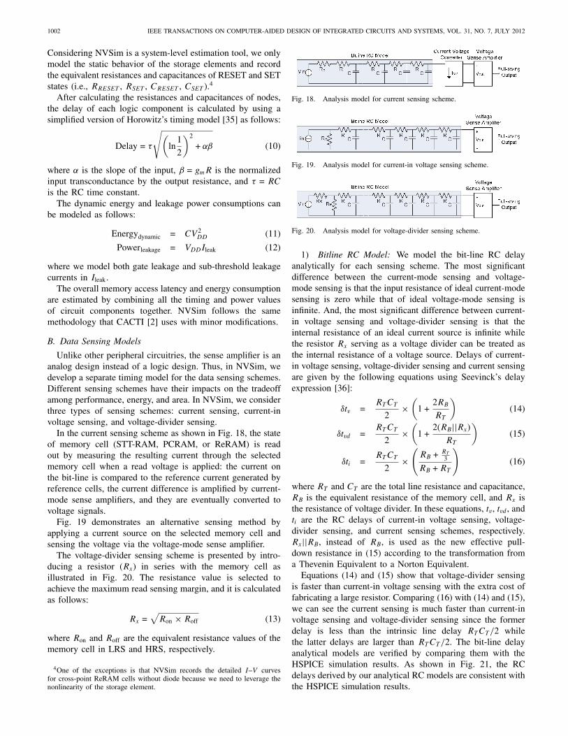
Fig. 17. Buffer designs with different transistor sizing. (a) Latency-optimized. (b) Balanced. (c) Area-optimized.
sizing methods rather than only applying logical effort. Inaddition, for some peripheral circuitry in NVM chips, the sizeof some transistors is determined by their required drivingcurrent instead of their capacitive load, and this violates thebasic rules of using logical effort.
Therefore, we offer three transistor sizing choices in thearea model of NVSim: one optimizing latency, one optimizingarea, while another balancing latency and area. An exampleis illustrated in Fig. 17 demonstrating the different sizingmethods when an output buffer with 4096 times the capac-itance of a minimum-sized inverter is to be designed. In alatency-optimized buffer design, the number of stages andall of the inverter sizing in the inverter chain is calculatedby logical effort to achieve minimum delay (30 units) whilepaying a huge area penalty (1365 units). In an area-optimizedbuffer design, there are only two stages of inverters, and thesize of the last stage is determined by the minimum drivingcurrent requirement. This type of buffer has the minimumarea (65 units), but is much slower than the latency-optimizedbuffer. The balanced option determines the size of last stageinverter by its driving current requirement and calculates thesize of the other inverters by logical effort. This results in abalanced delay and area metric.
V. Timing and Power Models
As an analytical modeling tool, NVSim uses RC analysis fortiming and power. In this section, we describe how resistancesand capacitances are estimated in NVSim and how they arecombined to calculate the delay and power consumption.
A. Generic Timing and Power Estimation
In NVSim, we consider the wire resistance and wire capac-itance from interconnects, turn-on resistance, switching resis-tance, gate and drain capacitances from transistors, and equiva-lent resistance and capacitance from memory storage elements(e.g., MTJ in STT-RAM and GST in PCRAM). The methodsof estimating wire and parasitic resistances and capacitancesare modified from the previous versions of CACTI [1], [2] byseveral enhancements. The enhancements include updating thetransistor models by latest ITRS report [15], considering thethermal impact on wire resistance calculation, adding drain-to-channel capacitance in the drain capacitance calculation, andso on. We build a look-up table to model the equivalent resis-tance and capacitance of memory storage elements since theyare the properties of certain nonvolatile memory technology.
1002 IEEE TRANSACTIONS ON COMPUTER-AIDED DESIGN OF INTEGRATED CIRCUITS AND SYSTEMS, VOL. 31, NO. 7, JULY 2012
Considering NVSim is a system-level estimation tool, we onlymodel the static behavior of the storage elements and recordthe equivalent resistances and capacitances of RESET and SETstates (i.e., RRESET , RSET , CRESET , CSET ).4
After calculating the resistances and capacitances of nodes,the delay of each logic component is calculated by using asimplified version of Horowitz’s timing model [35] as follows:
Delay = τ
√(ln
1
2
)2
+ αβ (10)
where α is the slope of the input, β = gmR is the normalizedinput transconductance by the output resistance, and τ = RC
is the RC time constant.The dynamic energy and leakage power consumptions can
be modeled as follows:
Energydynamic = CV 2DD (11)
Powerleakage = VDDIleak (12)
where we model both gate leakage and sub-threshold leakagecurrents in Ileak.
The overall memory access latency and energy consumptionare estimated by combining all the timing and power valuesof circuit components together. NVSim follows the samemethodology that CACTI [2] uses with minor modifications.
B. Data Sensing Models
Unlike other peripheral circuitries, the sense amplifier is ananalog design instead of a logic design. Thus, in NVSim, wedevelop a separate timing model for the data sensing schemes.Different sensing schemes have their impacts on the tradeoffamong performance, energy, and area. In NVSim, we considerthree types of sensing schemes: current sensing, current-involtage sensing, and voltage-divider sensing.
In the current sensing scheme as shown in Fig. 18, the stateof memory cell (STT-RAM, PCRAM, or ReRAM) is readout by measuring the resulting current through the selectedmemory cell when a read voltage is applied: the current onthe bit-line is compared to the reference current generated byreference cells, the current difference is amplified by current-mode sense amplifiers, and they are eventually converted tovoltage signals.
Fig. 19 demonstrates an alternative sensing method byapplying a current source on the selected memory cell andsensing the voltage via the voltage-mode sense amplifier.
The voltage-divider sensing scheme is presented by intro-ducing a resistor (Rx) in series with the memory cell asillustrated in Fig. 20. The resistance value is selected toachieve the maximum read sensing margin, and it is calculatedas follows:
Rx =√
Ron × Roff (13)
where Ron and Roff are the equivalent resistance values of thememory cell in LRS and HRS, respectively.
4One of the exceptions is that NVSim records the detailed I–V curvesfor cross-point ReRAM cells without diode because we need to leverage thenonlinearity of the storage element.
Fig. 18. Analysis model for current sensing scheme.
Fig. 19. Analysis model for current-in voltage sensing scheme.
Fig. 20. Analysis model for voltage-divider sensing scheme.
1) Bitline RC Model: We model the bit-line RC delayanalytically for each sensing scheme. The most significantdifference between the current-mode sensing and voltage-mode sensing is that the input resistance of ideal current-modesensing is zero while that of ideal voltage-mode sensing isinfinite. And, the most significant difference between current-in voltage sensing and voltage-divider sensing is that theinternal resistance of an ideal current source is infinite whilethe resistor Rx serving as a voltage divider can be treated asthe internal resistance of a voltage source. Delays of current-in voltage sensing, voltage-divider sensing and current sensingare given by the following equations using Seevinck’s delayexpression [36]:
δtv =RT CT
2×
(1 +
2RB
RT
)(14)
δtvd =RT CT
2×
(1 +
2(RB||Rx)
RT
)(15)
δti =RT CT
2×
(RB + RT
3
RB + RT
)(16)
where RT and CT are the total line resistance and capacitance,RB is the equivalent resistance of the memory cell, and Rx isthe resistance of voltage divider. In these equations, tv, tvd , andti are the RC delays of current-in voltage sensing, voltage-divider sensing, and current sensing schemes, respectively.Rx||RB, instead of RB, is used as the new effective pull-down resistance in (15) according to the transformation froma Thevenin Equivalent to a Norton Equivalent.
Equations (14) and (15) show that voltage-divider sensingis faster than current-in voltage sensing with the extra cost offabricating a large resistor. Comparing (16) with (14) and (15),we can see the current sensing is much faster than current-involtage sensing and voltage-divider sensing since the formerdelay is less than the intrinsic line delay RT CT /2 whilethe latter delays are larger than RT CT /2. The bit-line delayanalytical models are verified by comparing them with theHSPICE simulation results. As shown in Fig. 21, the RCdelays derived by our analytical RC models are consistent withthe HSPICE simulation results.

DONG et al.: NVSIM: A CIRCUIT-LEVEL PERFORMANCE, ENERGY, AND AREA MODEL 1003
TABLE II
Delay and Power Look-Up Table of Current−Voltage Converter
Process node 130 nm 90 nm 65 nm 45 nm 32 nm
Delay 0.49 ns 0.53 ns 0.62 ns 0.80 ns 1.07 ns
Dynamic energy per operation 8.52 × 10⁻¹⁴ J 8.72 × 10⁻¹⁴ J 9.00 × 10⁻¹⁴ J 10.26 × 10⁻¹⁴ J 12.56 × 10⁻¹⁴ J
Leakage power 1.40 × 10⁻⁸ W 1.87 × 10⁻⁸ W 2.57 × 10⁻⁸ W 4.41 × 10⁻⁸ W 12.54 × 10⁻⁸ W
Fig. 21. Delay model verification of three sensing schemes comparing toHSPICE simulations.
Fig. 22. Current–voltage converter modeled in NVSim.
2) Current–Voltage Converter Model: As shown in Fig. 18,the current–voltage converter in our current-mode sensingscheme is actually the first-level sense amplifier, and theCACTI-modeled voltage sense amplifier is still kept in thebitline model as the final stage of the sensing scheme. Thecurrent–voltage converter senses the current difference I1 − I2
and then it is converted into a voltage difference V1 − V2.The required voltage difference produced by current–voltageconverter is set by default to 80 mV. Although this valueis the minimum sensible voltage difference of the CACTI-modeled voltage sense amplifier, advanced user can overrideit for specific sense amplifier design. We refer to a previouscurrent–voltage converter design [36] and the circuit schematicis shown in Fig. 22. This sensing scheme is similar tothe hybrid-I/O approach [37], which can achieve high-speed,robust sensing, and low power operation.
To avoid unnecessary calculation, the current–voltage con-verter is modeled by directly using the HSPICE-simulatedvalues and building a look-up table of delay, dynamic energy,and leakage power (Table II).
C. Cell Switching Model
Different NVM technologies have their specific switch-ing mechanism. Usually, the switching phenomenon involvesmagnetoresistive, phase-change, thermochemical, and electro-chemical effects, and it cannot be estimated by RC analysis.Hence, the cell switching model in NVSim largely relies onthe NVM cell definition. The predefined NVM cell switchingproperties include the SET/RESET pulse duration (i.e., tSET
Fig. 23. Circuit schematic of the slow quench pulse shaper used in [10].
and tRESET) and SET/RESET current (i.e., ISET and IRESET) orvoltage. NVSim does not model the dynamic behavior duringthe switching of the cell state, the switching latency (i.e., cellwrite latency) is directly the pulse duration and the switchingenergy (i.e., cell write energy) is estimated using Joule’s firstlaw, that is
EnergySET = I2SETRtSET
EnergyRESET = I2RESETRtRESET (17)
in which the resistance value R can be the equivalent resistanceof the corresponding SET or RESET state (i.e., RSET orRRESET. However, for NVM technologies that have thresh-old switching phenomenon (e.g., PCRAM and ReRAM), theresistance value R always equals the resistance of the low-resistance state. This is because when a voltage above aparticular threshold is applied to these NVM cells in thehigh-resistance state, the resulting large electrical fields greatlyincrease the electrical conductivity [38].
VI. Miscellaneous Circuitry
Some specialized circuitry is required for certain types ofNVMs. For instance, some PCRAM chips need pulse shaper toreform accurate SET and RESET pulses, and NAND Flash andsome PCRAM chips need charge pump to generate the high-voltage power plane that is necessary for write operations.A. Pulse Shaper
Some PCRAM need specialized circuits to handle itsRESET and SET operations. Specific pulse shapes are requiredto heat up the GST quickly and to cool it down gradually,especially for SET operations. This pulse shaping requirementis achieved by using a slow quench pulse shaper. As shownin Fig. 23, the slow quench pulse shaper is composed of anarbitrary slow-quench waveform generator and a write driver.
In NVSim, the delay impacts of the slow quench shaperare neglected because they are already included in the RE-SET/SET calculation of the timing model. The energy impactsof the shaper is modeled by adding an energy efficiency duringthe RESET/SET operation, which we set the default value to35% [28] and it can be overridden by advanced user. Thearea of slow quench shapers is modeled by measuring the diephotos [10], [28].
1004 IEEE TRANSACTIONS ON COMPUTER-AIDED DESIGN OF INTEGRATED CIRCUITS AND SYSTEMS, VOL. 31, NO. 7, JULY 2012
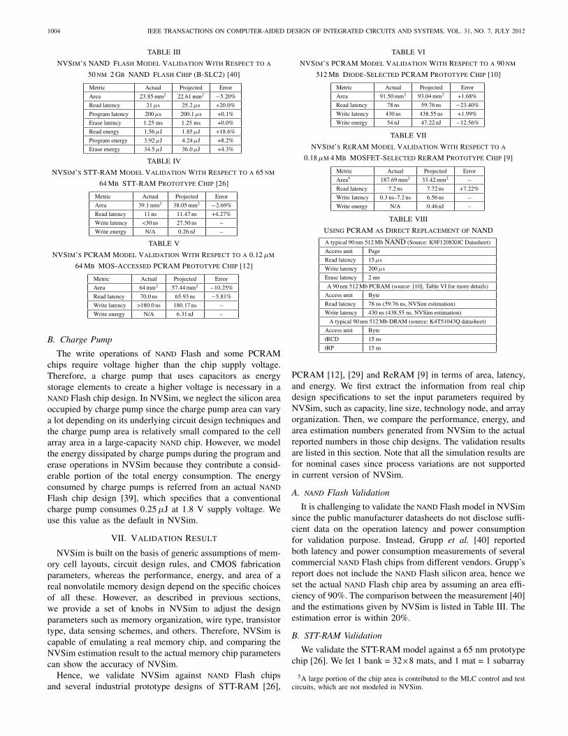
TABLE III
NVSim’s NAND Flash Model Validation With Respect to a
50 nm 2 Gb NAND Flash Chip (B-SLC2) [40]
Metric Actual Projected Error
Area 23.85 mm2 22.61 mm2 −5.20%
Read latency 21 μs 25.2 μs +20.0%
Program latency 200 μs 200.1 μs +0.1%
Erase latency 1.25 ms 1.25 ms +0.0%
Read energy 1.56 μJ 1.85 μJ +18.6%
Program energy 3.92 μJ 4.24 μJ +8.2%
Erase energy 34.5 μJ 36.0 μJ +4.3%
TABLE IV
NVSim’s STT-RAM Model Validation With Respect to a 65 nm
64 Mb STT-RAM Prototype Chip [26]
Metric Actual Projected Error
Area 39.1 mm2 38.05 mm2 −2.69%
Read latency 11 ns 11.47 ns +4.27%
Write latency <30 ns 27.50 ns –
Write energy N/A 0.26 nJ –
TABLE V
NVSim’s PCRAM Model Validation With Respect to a 0.12 μm
64 Mb MOS-Accessed PCRAM Prototype Chip [12]
Metric Actual Projected Error
Area 64 mm2 57.44 mm2 −10.25%
Read latency 70.0 ns 65.93 ns −5.81%
Write latency >180.0 ns 180.17 ns –
Write energy N/A 6.31 nJ –
B. Charge Pump
The write operations of NAND Flash and some PCRAMchips require voltage higher than the chip supply voltage.Therefore, a charge pump that uses capacitors as energystorage elements to create a higher voltage is necessary in aNAND Flash chip design. In NVSim, we neglect the silicon areaoccupied by charge pump since the charge pump area can varya lot depending on its underlying circuit design techniques andthe charge pump area is relatively small compared to the cellarray area in a large-capacity NAND chip. However, we modelthe energy dissipated by charge pumps during the program anderase operations in NVSim because they contribute a consid-erable portion of the total energy consumption. The energyconsumed by charge pumps is referred from an actual NAND
Flash chip design [39], which specifies that a conventionalcharge pump consumes 0.25 μJ at 1.8 V supply voltage. Weuse this value as the default in NVSim.
VII. Validation Result
NVSim is built on the basis of generic assumptions of mem-ory cell layouts, circuit design rules, and CMOS fabricationparameters, whereas the performance, energy, and area of areal nonvolatile memory design depend on the specific choicesof all these. However, as described in previous sections,we provide a set of knobs in NVSim to adjust the designparameters such as memory organization, wire type, transistortype, data sensing schemes, and others. Therefore, NVSim iscapable of emulating a real memory chip, and comparing theNVSim estimation result to the actual memory chip parameterscan show the accuracy of NVSim.
Hence, we validate NVSim against NAND Flash chipsand several industrial prototype designs of STT-RAM [26],
TABLE VI
NVSim’s PCRAM Model Validation With Respect to a 90 nm
512 Mb Diode-Selected PCRAM Prototype Chip [10]
Metric Actual Projected Error
Area 91.50 mm2 93.04 mm2 +1.68%
Read latency 78 ns 59.76 ns −23.40%
Write latency 430 ns 438.55 ns +1.99%
Write energy 54 nJ 47.22 nJ −12.56%
TABLE VII
NVSim’s ReRAM Model Validation With Respect to a
0.18 μm 4 Mb MOSFET-Selected ReRAM Prototype Chip [9]
Metric Actual Projected Error
Area5 187.69 mm2 33.42 mm2 –
Read latency 7.2 ns 7.72 ns +7.22%
Write latency 0.3 ns–7.2 ns 6.56 ns –
Write energy N/A 0.46 nJ –
TABLE VIII
Using PCRAM as Direct Replacement of NAND
A typical 90 nm 512 Mb NAND (Source: K9F1208X0C Datasheet)
Access unit Page
Read latency 15 μs
Write latency 200 μs
Erase latency 2 ms
A 90 nm 512 Mb PCRAM (source: [10], Table VI for more details)
Access unit Byte
Read latency 78 ns (59.76 ns, NVSim estimation)
Write latency 430 ns (438.55 ns, NVSim estimation)
A typical 90 nm 512 Mb DRAM (source: K4T51043Q datasheet)
Access unit Byte
tRCD 15 ns
tRP 15 ns
PCRAM [12], [29] and ReRAM [9] in terms of area, latency,and energy. We first extract the information from real chipdesign specifications to set the input parameters required byNVSim, such as capacity, line size, technology node, and arrayorganization. Then, we compare the performance, energy, andarea estimation numbers generated from NVSim to the actualreported numbers in those chip designs. The validation resultsare listed in this section. Note that all the simulation results arefor nominal cases since process variations are not supportedin current version of NVSim.
A. NAND Flash Validation
It is challenging to validate the NAND Flash model in NVSimsince the public manufacturer datasheets do not disclose suffi-cient data on the operation latency and power consumptionfor validation purpose. Instead, Grupp et al. [40] reportedboth latency and power consumption measurements of severalcommercial NAND Flash chips from different vendors. Grupp’sreport does not include the NAND Flash silicon area, hence weset the actual NAND Flash chip area by assuming an area effi-ciency of 90%. The comparison between the measurement [40]and the estimations given by NVSim is listed in Table III. Theestimation error is within 20%.
B. STT-RAM Validation
We validate the STT-RAM model against a 65 nm prototypechip [26]. We let 1 bank = 32×8 mats, and 1 mat = 1 subarray
5A large portion of the chip area is contributed to the MLC control and testcircuits, which are not modeled in NVSim.

DONG et al.: NVSIM: A CIRCUIT-LEVEL PERFORMANCE, ENERGY, AND AREA MODEL 1005
TABLE IX
New PCRAM Parameters After NVSim Latency Optimization
Parameter Before Optimization After Optimization
Subarray size 1024 × 1024 512 × 32
Area 93.04 mm2 102.34 mm2
Read latency 59.76 ns 16.23 ns
Write latency 438.55 ns 416.23 ns
to simulate the memory array organization. We also excludethe chip area of I/O pads and duplicated cells to make thefair comparison. As the write latency is not disclosed, weassume the write pulse duration is 20 ns. The validation resultis listed in Table IV. The result shows the area and the latencyestimation error is within 3% and 5%, respectively.
C. PCRAM Validation
We first validate the PCRAM model against a 0.12 μmMOS-accessed prototype. The array organization is configuredto have two banks, each has 8×8 mats. Every mat containsonly one subarray. Table V lists the validation result, whichshows a 10% underestimation of area and 6% underestimationof read latency. The projected write latency (SET latency asthe worst case) is also consistent with the actual value.
Another PCRAM validation is made against a 90 nm diode-accessed prototype [10].
D. ReRAM Validation
We validate the ReRAM model against a 180 nm 4 MbHfO2-based MOS-accessed ReRAM prototype [9]. Accordingto the disclosed data, the subarray size is configured to 128kb. We further model a bank with 4 × 8 mats and each matcontains a single subarray. The validation result is listed inTable VII. Note that the estimated chip area given by NVSimis much smaller than the actual value since the prototype chiphas SLC/MLC dual modes, but the current version of NVSimdoes not model the MLC-related circuitry.
E. Comparison to CACTI
We also test the closeness between NVSim and CACTI bysimulating identical SRAM caches and DRAM chips. Theresults show that NVSim models SRAM and DRAM moreaccurately than CACTI does since some false assumptions inCACTI are fixed in NVSim.
VIII. Case Studies by Using NVSim
In this section, we conduct two case studies to demonstratehow we can use NVSim in two ways: 1) use NVSim tooptimize the NVM designs toward certain design metric; and2) use NVSim to estimate the performance, energy, and areabefore fabricating a real prototype chip, especially when theemerging NVM device technology is still under developmentand there is no standard so far.
A. Use NVSim for Design Optimization
NAND Flash is currently the widely-used firmware storageor disk in embedded systems. However, codes stored in NAND
must be copied to random-accessible memory like DRAMbefore execution since NAND’s page-accessible structure causespoor random access performance. If emerging NVM technolo-gies such as STT-RAM, PCRAM, and ReRAM can be adopted
TABLE X
Projection of a Future ReRAM Technology
MOS-Accessed Cross-Point
Cell size 4F 2 20F 2
Maximum NMOS driver size 100 F
RESET voltage and pulse duration 2.0 V, 100 ns
SET voltage and pulse duration −2.0 V, 100 ns
READ input0.4 V voltage source,
or 2 μA current source
LRS resistance 10 k�
HRS resistance 500 k�
Half-select resistance – 100 k�
in such systems, their byte-accessibility property can eliminatethe need of DRAM modules in such systems. But, the issueof directly adopting emerging NVM technologies as the NAND
Flash substitute comes from the observation that the currentprototype has a much slower read/write latency than DRAM.In this case study, we use PCRAM as an example withoutthe loss of generality. The technology node used in this casestudy is 90 nm. Table VIII shows the latency difference amonga NAND chip, a DRAM chip, and a PCRAM prototype chipwith the same 512 Mb capacity.
The comparison shows the PCRAM prototype chip is muchslower than its DRAM counterpart. To overcome this obstacle,it is necessary to optimize PCRAM chips for latency at theexpense of area efficiency by aggressively cutting wordlinesand bitlines or inserting repeaters. Such area/performancetradeoff is also available for DRAM designs. However, in thiscase study, we keep the DRAM chip parameters unchangedsince the current DRAM specification is already the sweet-spot explored by DRAM industry for many years. But forPCRAM, such performance optimization is necessary.
Table IX shows the comparison before and after NVSimoptimization. The result shows the PCRAM read latency canbe reduced from 59.76 ns to 16.23 ns by only cutting subarraysinto smaller size (from 1024×1024 to 512×32). Although thePCRAM write latency does not reduce too much due to theinherent SET/RESET pulse duration, write latency is typicallynot in the critical path and can be tolerated using write buffers.As a result, the optimized PCRAM chip projected by NVSimcan properly replace the traditional NAND+DRAM solutionin the embedded system. The latency optimization is at theexpense of increasing chip area, which rises from 93.04 mm2
to 102.34 mm2.
B. Use NVSim for Early Stage Estimation
Considering the facts that the research of some emergingNVM technologies (e.g., ReRAM) is still in an early stageand there are only a limited number of NVM prototype chipsavailable for high-level computer architects understanding thetechnologies, we expect NVSim would be helpful in providingperformance, energy, and area estimations at an early designstage. In this case study, we demonstrate how NVSim canpredict the full design spectrum of a projected ReRAM tech-nology when such a device is fabricated as an 8 MB memorychip. Table X lists the projection.
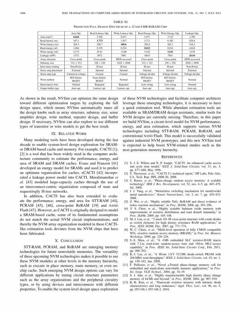
Table XI tabulates the full design spectrum of this 32 nm8 MB ReRAM chip by listing the details of each design corner.
1006 IEEE TRANSACTIONS ON COMPUTER-AIDED DESIGN OF INTEGRATED CIRCUITS AND SYSTEMS, VOL. 31, NO. 7, JULY 2012
TABLE XI
Predicted Full Design Spectrum of a 32 nm 8 MB ReRAM Chip
Area Opt. Read Latency Opt. Write Latency Opt. Read Energy Opt. Write Energy Opt. Leakage Opt.
Area (mm2) 0.664 5.508 8.071 2.971 3.133 1.399
Read latency (ns) 107.1 1.773 1.917 5.711 6.182 426.8
Write latency (ns) 204.3 200.7 100.6 202.8 203.1 518.2
Read energy (nJ) 1.884 0.195 0.234 0.012 0.014 4.624
Write energy (nJ) 13.72 25.81 13.06 12.82 12.81 12.99
Leakage (mW) 1372 3872 7081 6819 7841 26.64
Array structure Cross-point Cross-point MOS-accessed Cross-point Cross-point MOS-accessed
Subarray size 512 × 512 128 × 128 1024 × 2048 512 × 512 256 × 256 2048 × 4096
Inter-array routing Non-H-tree H-tree H-tree H-tree H-tree Non-H-tree
Sense amp placement External Internal Internal Internal Internal External
Sense amp type Current-in voltage Current Current Voltage-divider Voltage-divider Voltage-divider
Write methodSET-before- Erase-before-
NormalSET-before- SET-before-
NormalRESET RESET RESET RESET
Interconnect wire Normal Repeated Repeated Low-swing Low-swing Normal
Output buffer type Area opt. Latency opt. Latency opt. Area opt. Area opt. Area opt.
As shown in the result, NVSim can optimize the same designtoward different optimization targets by exploring the fulldesign space, which means NVSim automatically tunes allthe design knobs such as array structure, subarray size, senseamplifier design, write method, repeater design, and bufferdesign. If necessary, NVSim can also explore to use differenttypes of transistor or wire models to get the best result.
IX. Related Work
Many modeling tools have been developed during the lastdecade to enable system-level design exploration for SRAM-or DRAM-based cache and memory. For example, CACTI [1],[2] is a tool that has been widely used in the computer archi-tecture community to estimate the performance, energy, andarea of SRAM and DRAM caches. Evans and Franzon [41]developed an energy model for SRAMs and used it to predictan optimum organization for caches. eCACTI [42] incorpo-rated a leakage power model into CACTI. Muralimanohar etal. [43] modeled large-capacity caches through the use ofan interconnect-centric organization composed of mats andrequest/reply H-tree networks.
In addition, CACTI has also been extended to evalu-ate the performance, energy, and area for STT-RAM [44],PCRAM [45], [46], cross-point ReRAM [19] and NAND
Flash [47]. However, as CACTI is originally designed to modela SRAM-based cache, some of its fundamental assumptionsdo not match the actual NVM circuit implementations, andthereby the NVM array organization modeled in these CACTI-like estimation tools deviates from the NVM chips that havebeen fabricated.
X. Conclusion
STT-RAM, PCRAM, and ReRAM are emerging memorytechnologies for future nonvolatile memories. The versatilityof these upcoming NVM technologies makes it possible to usethese NVM modules at other levels in the memory hierarchy,such as execute in place memory, main memory, or even on-chip cache. Such emerging NVM design options can vary fordifferent applications by tuning circuit structure parameterssuch as the array organizations and the peripheral circuitrytypes, or by using devices and interconnects with differentproperties. To enable the system-level design space exploration
of these NVM technologies and facilitate computer architectsleverage these emerging technologies, it is necessary to havea quick estimation tool. While abundant estimation tools areavailable as SRAM/DRAM design assistants, similar tools forNVM designs are currently missing. Therefore, in this paperwe build NVSim, a circuit-level model for NVM performance,energy, and area estimation, which supports various NVMtechnologies including STT-RAM, PCRAM, ReRAM, andconventional NAND Flash. This model is successfully validatedagainst industrial NVM prototypes, and this new NVSim toolis expected to help boost NVM-related studies such as thenext-generation memory hierarchy.
References
[1] S. J. E. Wilton and N. P. Jouppi, “CACTI: An enhanced cache accessand cycle time model,” IEEE J. Solid-State Circuits, vol. 31, no. 5,pp. 677–688, May 1996.
[2] S. Thoziyoor, et al., “CACTI 5.1 technical report,” HP Labs, Palo Alto,CA, Tech. Rep. HPL-2008-20, 2008.
[3] S. Raoux, et al., “Phase-change random access memory: A scalabletechnology,” IBM J. Res. Development, vol. 52, nos. 4–5, pp. 465–479,Jul. 2008.
[4] J. J. Yang, et al., “Memristive switching mechanism for metal/oxide/metal nanodevices,” Nature Nanotechnol., vol. 3, no. 7, pp. 429–433,2008.
[5] Z. Wei, et al., “Highly reliable TaOx ReRAM and direct evidence ofredox reaction mechanism,” in Proc. IEDM, 2008, pp. 293–296.
[6] Y. S. Chen, et al., “Highly scalable hafnium oxide memory withimprovements of resistive distribution and read disturb immunity,” inProc. IEDM, 2009, pp. 105–108.
[7] M.-J. Lee, et al., “2-stack 1D-1R cross-point structure with oxide diodesas switch elements for high density resistance RAM applications,” inProc. IEEE IEDM, Dec. 2007, pp. 771–774.
[8] W. C. Chien, et al., “Multi-level operation of fully CMOS compatibleWOx resistive random access memory (RRAM),” in Proc. Int. MemoryWorkshop, 2009, pp. 228–229.
[9] S.-S. Sheu, et al., “A 4 Mb embedded SLC resistive-RAM macrowith 7.2 ns read-write random-access time and 160 ns MLC-accesscapability,” in Proc. IEEE Int. Solid-State Circuits Conf., Feb. 2011,pp. 200–202.
[10] K.-J. Lee, et al., “A 90 nm 1.8 V 512 Mb diode-switch PRAM with266 MB/s read throughput,” IEEE J. Solid-State Circuits, vol. 43, no. 1,pp. 150–162, Jan. 2008.
[11] F. Pellizzer, et al., “Novel μTrench phase-change memory cell forembedded and stand-alone nonvolatile memory applications,” in Proc.Int. Symp. VLSI Technol., 2004, pp. 18–19.
[12] S. J. Ahn, et al., “Highly manufacturable high density phase changememory of 64 Mb and beyond,” in Proc. IEDM, 2004, pp. 907–910.
[13] K.-H. Kim, et al., “Nanoscale resistive memory with intrinsic diodecharacteristics and long endurance,” Appl. Phys. Lett., vol. 96, no. 5,pp. 053 106.1–053 106.3, 2010.
DONG et al.: NVSIM: A CIRCUIT-LEVEL PERFORMANCE, ENERGY, AND AREA MODEL 1007
[14] H. Y. Lee, et al., “Evidence and solution of over-RESET problem forHfOx based resistive memory with sub-ns switching speed and highendurance,” in Proc. IEDM, 2010, pp. 19.7.1–19.7.4.
[15] International Technology Roadmap for Semiconductors. (2010). ProcessIntegration, Devices, and Structures Update [Online]. Available:http://www.itrs.net
[16] C. W. Smullen, et al., “Relaxing non-volatility for fast and energy-efficient STT-RAM caches,” in Proc. Int. Symp. High PerformanceComput. Architecture, Feb. 2011, pp. 50–61.
[17] D.-C. Kau, et al., “A stackable cross point phase change memory,” inProc. IEEE IEDM, Dec. 2009, pp. 27.1.1–27.1.4.
[18] Y.-C. Chen, et al., “An access-transistor-free (0T/1R) non-volatileresistance random access memory (RRAM) using a novel thresholdswitching, self-rectifying chalcogenide device,” in Proc. IEDM, 2003,pp. 750–753.
[19] C. Xu, et al., “Design implications of memristor-based RRAMcross-point structures,” in Proc. Des. Autom. Test Eur., 2011, pp. 1–6.
[20] S. Thoziyoor, et al., “A comprehensive memory modeling tool and itsapplication to the design and analysis of future memory hierarchies,”in Proc. Int. Symp. Comput. Architecture, 2008, pp. 51–62.
[21] International Technology Roadmap for Semiconductors. The Model forAssessment of CMOS Technologies and Roadmaps (MASTAR) [Online].Available: http://www.itrs.net/models.html
[22] A. Udipi, et al., “Rethinking DRAM design and organization forenergy-constrained multi-cores,” ACM SIGARCH Comput. ArchitectureNews, vol. 38, no. 3, pp. 175–186, 2010.
[23] J. Liang and H. S. P. Wong, “Cross-point memory array without cellselectors: Device characteristics and data storage pattern dependencies,”IEEE Trans. Electron Devices, vol. 57, no. 10, pp. 2531–2538, Oct.2010.
[24] M. Hosomi, et al., “A novel nonvolatile memory with spin torquetransfer magnetization switching: Spin-RAM,” in Proc. IEDM, 2005,pp. 459–462.
[25] T. Kawahara, et al., “2 Mb spin-transfer torque RAM (SPRAM) withbit-by-bit bidirectional current write and parallelizing-direction currentread,” in Proc. IEEE Int. Solid-State Circuits Conf., Feb. 2007, pp.480–617.
[26] K. Tsuchida, et al., “A 64 Mb MRAM with clamped-reference andadequate-reference schemes,” in Proc. Int. Solid-State Circuits Conf.,2010, pp. 268–269.
[27] H.-R. Oh, et al., “Enhanced write performance of a 64-Mb phase-change random access memory,” IEEE J. Solid-State Circuits, vol. 41,no. 1, pp. 122–126, Jan. 2006.
[28] S. Hanzawa, et al., “A 512 kB embedded phase change memory with416 kB/s write throughput at 100 μA cell write current,” in Proc. Int.Solid-State Circuits Conf., 2007, pp. 474–616.
[29] S. Kang, et al., “A 0.1 μm 1.8 V 256 Mb phase-change random accessmemory (PRAM) with 66 MHz synchronous burst-read operation,”IEEE J. Solid-State Circuits, vol. 42, no. 1, pp. 210–218, Jan.2007.
[30] F. Fishburn, et al., “A 78 nm 6 F2 DRAM technology for multigigabitdensities,” in Proc. Symp. VLSI Technol., 2004, pp. 28–29.
[31] J. H. Oh, et al., “Full integration of highly manufacturable 512 MbPRAM based on 90 nm technology,” in Proc. IEDM, 2006, pp. 49–52.
[32] Y. Zhang, et al., “An integrated phase change memory cell with Genanowire diode for cross-point memory,” in Proc. IEEE Symp. VLSITechnol., Jun. 2007, pp. 98–99.
[33] Y. Sasago, et al., “Cross-point phase change memory with 4F2 cell sizedriven by low-contact-resistivity poly-Si diode,” in Proc. Symp. VLSITechnol., 2009, pp. 24–25.
[34] I. E. Sutherland, R. F. Sproull, and D. Harris, Logical Effort: DesigningFast CMOS Circuits. San Francisco, CA: Morgan Kaufmann,1999.
[35] M. A. Horowitz, “Timing models for MOS circuits,” StanfordUniversity, Stanford, CA, Tech. Rep. SEL-TR-83-003, 1983.
[36] E. Seevinck, P. J. van Beers, and H. Ontrop, “Current-mode techniquesfor high-speed VLSI circuits with application to current sense amplifierfor CMOS SRAM’s,” IEEE J. Solid-State Circuits, vol. 26, no. 4, pp.525–536, Apr. 1991.
[37] Y. Moon, et al., “1.2 V 1.6 Gb/s 56 nm 6F2 4 Gb DDR3 SDRAM withhybrid-I/O sense amplifier and segmented sub-array architecture,” inProc. Int. Solid-State Circuits Conf., 2009, pp. 128–129.
[38] G. W. Burr, et al., “Phase change memory technology,” J. Vac. Sci.Technol. B, vol. 28, no. 2, pp. 223–262, 2010.
[39] K. Ishida, et al., “A 1.8 V 30 nJ adaptive program-voltage (20 V)generator for 3D-integrated NAND Flash SSD,” in Proc. IEEE Int.Solid-State Circuits Conf., Feb. 2009, pp. 238–239, 239a.
[40] L. M. Grupp, et al., “Characterizing Flash memory: Anomalies,observations, and applications,” in Proc. Int. Symp. Microarchitecture,2009, pp. 24–33.
[41] R. J. Evans and P. D. Franzon, “Energy consumption modeling andoptimization for SRAMs,” IEEE J. Solid-State Circuits, vol. 30, no. 5,pp. 571–579, May 1995.
[42] M. Mamidipaka and N. Dutt, “eCACTI: An enhanced power estimationmodel for on-chip caches,” Center Embedded Comput. Syst., Univ.California, Irvine, Tech. Rep. TR04-28, 2004.
[43] N. Muralimanohar, R. Balasubramonian, and N. P. Jouppi, “Architectingefficient interconnects for large caches with CACTI 6.0,” IEEE Micro,vol. 28, no. 1, pp. 69–79, Jan.–Feb. 2008.
[44] X. Dong, et al., “Circuit and microarchitecture evaluation of 3-Dstacking magnetic RAM (MRAM) as a universal memory replacement,”in Proc. Des. Autom. Conf., 2008, pp. 554–559.
[45] P. Mangalagiri, et al., “A low-power phase change memory basedhybrid cache architecture,” in Proc. Great Lakes Symp. VLSI, 2008, pp.395–398.
[46] X. Dong, N. P. Jouppi, and Y. Xie, “PCRAMsim: System-levelperformance, energy, and area modeling for phase-change RAM,” inProc. Int. Conf. Comput.-Aided Des., 2009, pp. 269–275.
[47] V. Mohan, S. Gurumurthi, and M. R. Stan, “FlashPower: A detailedpower model for NAND Flash memory,” in Proc. Des. Autom. TestEur., 2010, pp. 502–507.
Xiangyu Dong (S’09–M’12) received the B.S. de-gree in electronic engineering from Shanghai JiaoTong University, Shanghai, China, in 2006, and thePh.D. degree in computer science and engineeringfrom Pennsylvania State University, University Park,in 2011.
He is currently a Senior Engineer with Qualcomm,Inc., San Diego, CA. His current research interestsinclude computer architectures, emerging nonvolatilememory, and 3-D integration technology.
Cong Xu (S’09) received the B.S. degree fromPeking University, Beijing, China, and joined Penn-sylvania State University, University Park, in 2009,where he is currently pursuing the Ph.D. degree withthe Department of Computer Science and Engineer-ing.
His current research interests include nonvolatilememory system design based on emerging memorytechnologies, low power very large scale integrationdesign, and computer architectures.
Yuan Xie (SM’07) received the B.S. degree in elec-tronic engineering from Tsinghua University, Bei-jing, China, in 1997, and the M.S. and Ph.D. degreesin electrical engineering from Princeton University,Princeton, NJ, in 1999 and 2002, respectively.
He is currently an Associate Professor with theDepartment of Computer Science and Engineering,Pennsylvania State University, University Park. Be-fore joining Pennsylvania State University in 2003,he was with the IBM Microelectronic Division,Worldwide Design Center, Essex Juction, VT. His
current research interests include very large scale integration design, computerarchitectures, embedded systems design, and electronic design automation.
Dr. Xie is a Senior Member of ACM. He received the SRC InventorRecognition Award in 2002 and the U.S. National Science FoundationFaculty Early Career Development Award in 2006.
Norman P. Jouppi (F’03) received the Ph.D. degreein electrical engineering from Stanford University,Stanford, CA.
He is a Fellow and the Director of the In-telligent Infrastructure Laboratory, Hewlett-PackardLabs, Palo Alto, CA. His current research inter-ests include computer memory systems, networkingfor cluster computing, blade system architectures,graphics accelerators, video, audio, and physicaltelepresence.
Dr. Jouppi is a Fellow of ACM.