a model for chemical–mechanical polishing of a material
TRANSCRIPT

Journal of the Mechanics and Physics of Solids52 (2004) 847–873
www.elsevier.com/locate/jmps
A model for chemical–mechanical polishing of amaterial surface based on contact mechanics
J.J. Vlassak∗
Division of Engineering and Applied Sciences, Harvard University, 29 Oxford Street, Cambridge,MA 02138, USA
Received 27 May 2003; accepted 31 July 2003
Abstract
A new contact-mechanics-based model for chemical–mechanical polishing is presented. Ac-cording to this model, the local polish rate is controlled by the pressure distribution betweenfeatures on the wafer and the polishing pad. The model uses an analysis based on the workby Greenwood to evaluate this pressure distribution taking into account pad compliance androughness. Using the model, the e2ects of pattern density, applied down-force, selectivity, padproperties, etc. on the evolution of the wafer surface can be readily evaluated. The interactionbetween individual pad asperities and the wafer pattern is investigated in detail. It is shown thatthe pressure distribution between an asperity and the wafer surface is discontinuous at edges offeatures that have di2erent nominal polish rates and that this pressure discontinuity dominatesthe polish rate and dishing of narrow features.
The model is implemented as an algorithm that calculates the evolution of the pro4le of a setof features on the wafer during the polishing process. The model can be applied to chemical–mechanical polishing used for oxide planarization, metal damascene or shallow trench isolation.? 2003 Elsevier Ltd. All rights reserved.
Keywords: A: Wear and ablation; B: Chemical mechanical polishing; Contact mechanics
1. Introduction
With the advent of shallow trench isolation (STI) and copper interconnects, chemical–mechanical polishing (CMP) has emerged as one of the most important operations inthe fabrication of integrated circuits. In the CMP process, an abrasive slurry is used topolish a patterned Si wafer on a polishing pad in order to selectively remove material
∗ Tel.: +1-617-496-0424; fax: +1-617-496-0601.E-mail address: [email protected] (J.J. Vlassak).
0022-5096/$ - see front matter ? 2003 Elsevier Ltd. All rights reserved.doi:10.1016/j.jmps.2003.07.007

848 J.J. Vlassak / J. Mech. Phys. Solids 52 (2004) 847–873
from the wafer surface. This material can be a metal or a dielectric. The goal of thisprocess is then to either planarize the wafer (e.g. dielectric CMP) or to de4ne a patternin the wafer surface (e.g. metal damascene or STI). In spite of its apparent simplicity,CMP is a very complicated process in which both mechanical and chemical factorsplay an important role. The removal rate during the polishing process depends sensi-tively on pattern geometry and density, and CMP may result in excessive erosion of thedielectric layer or dishing of metal lines if the process is not properly controlled. Sincesurface topography has a signi4cant impact on wafer yield, numerous attempts havebeen made to predict the evolution of the wafer pro4le during the polishing process.One of the 4rst models that allowed quantitative predictions of wafer topography is a
phenomenological model proposed by Warnock (1991). In this model, the removal rateat a given point is a2ected by the surrounding wafer topography. If the surroundingfeatures are higher, the removal rate is reduced; if they are lower, the removal rateis enhanced. The model makes use of a number of 4tting parameters that are relatedto pad compressibility and roughness, but that do not have a direct physical meaning.While useful in practice for predicting dishing and erosion, this type of model doesnot provide much insight in the actual CMP process.Recently several mechanic-based models have been proposed. These models can be
regarded as either wafer-scale (Sundararajan et al., 1999; Tichy et al., 1999; Thakurtaet al., 2000) or feature-scale (Runnels, 1994; Chekina et al., 1998). Wafer-scale modelsare usually concerned with the pressure distribution between wafer and polishing padand with the uniformity of the removal rate across a wafer. Sundararajan et al. (1999)and Thakurta et al. (2000) recently developed a sophisticated wafer-scale model thatrelies on slurry hydrodynamics. In this model, lubrication theory is used to relate slurry4lm thickness and pressure. The model takes into account compressibility of the pad andthe mode of slurry delivery to the polishing pad. The CMP removal rate is calculatedusing a mass transport model. The model seems to give reasonable predictions ofremoval rate as long as the CMP process takes place in the lubrication regime wherethe wafer is not in direct contact with the pad. Tichy et al. (1999) developed anothermodel in which the CMP process is regarded as a contact problem of a wafer on arough pad lubricated by a slurry. The slurry 4lm thickness is controlled by the heightof the pad asperities and Reynolds equation is used to calculate interfacial pressure.This model has been successful at predicting experimentally measured pressure pro4les(Shan et al., 1999).Feature-scale models describe how individual features on a wafer change during
the polishing process. This is of some import since erosion of dielectric or dishingof metal features have an adverse e2ect on wafer yield. Runnels (1994) has devel-oped a Euid-based wear model in which there is a continuous slurry layer betweenwafer and pad. The Eow of the slurry 4lm is analyzed and the removal rate is as-sumed to be a function of the shear stress induced at the wafer surface. Chekinaet al. (1998) have used an approach developed in contact mechanics to analyze featureshape and pressure pro4le evolution during the CMP process. In this model the pres-sure distribution between wafer and pad is determined by the elastic deformation of thepolishing pad, which thus plays an important role in determining the 4nal wafer surfacepro4le.

J.J. Vlassak / J. Mech. Phys. Solids 52 (2004) 847–873 849
Boning et al. (1999) have developed a model to calculate the wafer surface pro4leat a length scale comparable to the size of a die, i.e. intermediate between feature andwafer scale. In this model, the removal rate depends on the e2ective pattern density,which is calculated from the wafer topography using a procedure based on contactmechanical considerations. This model is a useful tool for developing integrated circuitlayouts, but it is mostly phenomenological and does not provide much physical insight.The e2ect of polishing pad roughness has been considered by Yu et al. (1993) whoused a statistical approach to model the interaction between pad asperities and wafer.In this model, they considered contact between planar surfaces only and did not takeinto account pad deformation.In this article, a new model is presented to describe the evolution of the wafer sur-
face during the CMP process. The model determines the average pressure distributionbetween polishing pad and wafer at the feature scale. This pressure distribution is thenused to determine the local removal rate. The roughness of the polishing pad is mod-eled using an approach 4rst developed by Greenwood and coworkers (Greenwood andWilliamson, 1966; Greenwood and Tripp, 1967). Elastic deformation of the pad due tothe non-planar topography of the wafer is taken into account using a contact-mechanicsanalysis. The model is then used to study dielectric erosion and metal dishing or recessas a function of CMP process parameters and wafer pattern geometry. In the secondpart of the article, the interaction between individual pad asperities and the wafer pat-tern is investigated in detail. It will be shown that discontinuities in the nominal polishrate, e.g. at the edge of a metal line, have a signi4cant impact on the local pressuredistribution and hence the evolution of the wafer surface.
2. Model description
Fig. 1 illustrates the CMP model described in this article. The polishing process ismodeled as a process in which a compliant polishing pad contacts the patterned surfaceof a rigid wafer. The pad is assumed to be linearly elastic and show no viscoelastice2ects. The surface of the pad is rough and contains asperities with a given heightdistribution. It is further assumed that the abrasive particles in the slurry are muchsmaller than the pad asperities, which is indeed the case for most commercial CMP
x
z
S(x, y, t)
d(x, y, t)
w(x, y, t)
Wafer
Pad
Metal
Fig. 1. Schematic representation of the contact model.

850 J.J. Vlassak / J. Mech. Phys. Solids 52 (2004) 847–873
processes. When the wafer is pressed against the pad, some of the pad asperities con-tact the wafer directly, transferring the force from the wafer to the pad and elasticallydeforming the polishing pad. The pressure in the slurry is assumed to be constant atthe length scale under consideration and hence does not contribute to variations in paddeEection. There is some experimental evidence that this is indeed the case (Shanet al., 1999). The contact pressure between pad and wafer is then calculated us-ing the approach formulated by Greenwood and Williamson (1966) and Greenwoodand Tripp (1967). Once the contact pressure is known, the local removal rate isdetermined.The heights of the pad asperities are described by an exponential distribution func-
tion:
P(z) =12�
exp(− |z|
�
); (1)
where z is the height of the asperity above or below the pad surface. The variable �is a characteristic roughness parameter that represents the width of the asperity heightdistribution and can be measured for a given polishing pad. Experimental data (Yuet al., 1993) suggest that a Gaussian distribution would give a more accurate descrip-tion of the height distribution. The exponential distribution, however, has signi4cantcomputational advantages and is expected to give similar results (Johnson, 1985). Thetops of the asperities are taken to be spherical, all with the same curvature �. In reality,the curvatures take random values and the average curvature can be used for �. Thisprocedure is not exact since the asperity height and curvature are strictly not inde-pendent parameters, but the approximation has been justi4ed by Onions and Archard(1973).When the wafer is pressed against the polishing pad, asperities with heights greater
than the gap between wafer and pad will be compressed and transfer load from thewafer to the pad, which in turn will deform elastically. If w(x; y; t) represents theshape of the deformed pad surface at time t, then the gap between pad surface andwafer is
d(x; y; t) = w(x; y; t)− S(x; y; t); (2)
where S(x; y; t) is a function that describes the wafer surface at time t (see Fig. 1). Ifthe asperities deform elastically according to the laws governing Hertzian contacts, theforce transmitted by an individual asperity of height z is given by
F =4
3√�
E1− �2
(z − d(x; y; t))3=2; (3)
where E and � are Young’s modulus and Poisson’s ratio of the pad, respectively. Theaverage pressure between wafer and pad due to all pad asperities in contact with thewafer is then
p(x; y; t) =4�3√�
E1− �2
∫ ∞
d(x;y; t)(z − d(x; y; t))3=2
12�
exp(− |z|
�
)dz; (4)

J.J. Vlassak / J. Mech. Phys. Solids 52 (2004) 847–873 851
where � is the asperity density. After a change of variables, the integral can be readilycalculated leading to the following expression for the pressure distribution:
p(x; y; t) =
√��3�2√�
E1− �2
exp(− w(x; y; t)− S(x; y; t)
�
)for w − S¿ 0: (5)
If the deformation of the pad w(x; y; t) is known, the pressure distribution betweenwafer and pad can be obtained from Eq. (5).The deformation of the polishing pad in turn can be related to the pressure distri-
bution using equations derived in contact mechanics. If a pressure p(x; y; t) is appliedover an area A of a half space, the displacement, w(x; y; t), of the surface of the halfspace is given by the following formula (Johnson, 1985):
w(x; y; t) =1− �2
�E
∫Ap(�; �; t)
1√(�− x)2 + (�− y)2
d� d�: (6)
If the length scale over which we consider the deformation of the pad is small comparedto the thickness of the polishing pad, Eq. (6) can be used to determine the deEection ofthe pad. Eqs. (5) and (6) then constitute a set of two equations describing the pressuredistribution and ensuing pad deEection for a given wafer surface topography S(x; y; t).
If the pattern on the wafer consists of an array of parallel lines, the computationale2ort involved in determining the pressure pro4le from Eqs. (5) and (6) can be sig-ni4cantly reduced by representing the pattern as a two-dimensional periodic structure.Using this approach, a wide range of surface pro4les can be simulated, from an iso-lated line in a 4eld to a periodic array of dense lines. The plane-strain deformation,w(x; t), of a half-space under a periodic pressure distribution is given by the followingequation (Johnson, 1985; Gradshtein and Ryzhik, 1994):
dwdx
=−2(1− �2)LE
∫ L=2
−L=2p(s; t) cot
�(x − s)L
ds; (7)
where L is the repeat length or period of the structure. After integrating Eq. (7), oneobtains the following expression for w(x; t):
w(x; t)− C(t) =−2(1− �2)�E
∫ L=2
−L=2p(s; t) ln
∣∣∣∣sin �(x − s)L
∣∣∣∣ ds; (8)
where C(t) is an integration constant. Eqs. (5) and (8) again form a set of two equa-tions from which the pressure distribution and pad deEection can be calculated. Itshould be noted that Eq. (8) gives the shape of the pad only within an integrationconstant C(t). This is typical for plane-strain contact problems. In this case, the valueof C(t) can be determined from the requirement that the pressure distribution integratedover one period be equal to the load applied to the corresponding section of the wafer.One of the diJculties in analyzing contact problems is that the area of contact
between the two objects is not known a priori. The present model does not su2er fromthis problem since the pad is assumed to be everywhere in contact with the wafer viathe pad asperities. Since in theory the asperity height can take on any arbitrary value,

852 J.J. Vlassak / J. Mech. Phys. Solids 52 (2004) 847–873
one can always 4nd an asperity that will bridge the gap between the wafer and thepad independent of how large that gap is. The wafer is therefore always in indirectcontact with the pad. If the gap is very large, however, asperities bridging the gap willbe very rare and little or no load will be transferred between the wafer and the pad.The material removal rate in CMP generally depends on many parameters including
the contact pressure between wafer and polishing pad, the relative velocity of the waferwith respect to the pad, the temperature T , and the nature of the abrasive slurry. Thelocal removal or wear rate can thus be represented by a function
R(x; y; t) = f(p(x; y; t); v(x; y; t); T (x; y; t); : : :): (9)
The form of f depends on the details of the CMP process. Often a linear relationshipis observed (Cook, 1990; Kaufman et al., 1991), although non-linear behavior has alsobeen reported (Tseng and Wang, 1997). The simplest linear relationship between wearrate, pressure, and velocity is known as Preston’s law and is given by
R(x; y; t) = k(x; y; t)v(x; y; t)p(x; y; t); (10)
where k(x; y; t) is the wear coeJcient. If the wafer surface consists of di2erent materi-als, the wear coeJcient is a function of position. It should be noted that in the currentmodel any chemical e2ects in the CMP process are captured by the wear coeJcient.Slurry chemistry, for instance, has a signi4cant impact on the removal rate and henceon the value of k. Finally, the removal rate is directly linked to local changes in wafershape:
R(x; y; t) =−@S(x; y; t)@t
: (11)
Integration of Preston’s equation yields the evolution of the surface pro4le S(x; y; t) asa function of time. Note that Preston’s law is used in the present formulation of themodel, but this is not essential to the model and any wear law in which the removalrate increases monotonously with pressure could be used instead. Qualitatively, theresults remain the same.Eqs. (5), (10), and (11) together with Eqs. (8) or (6) depending on whether the
problem is respectively two or three-dimensional, describe the evolution of the wafersurface during the polishing process. It is interesting to consider the behavior of thismodel for limiting values of the parameter �. If the pad is very rough compared to therelief on the wafer, i.e. � is much larger than w−S, then the pressure pro4le is nearlyconstant and the removal rate depends only on the local value of the wear coeJcientk(x; y; t) in Preston’s law. If, on the other hand, the pad surface is very smooth, �approaches zero. In that case, Eq. (5) shows that the pressure is 4nite when there isno gap between wafer and polishing pad, and zero otherwise. Any changes in surfacerelief of the wafer can then be attributed to compression of the pad in addition to wearcoeJcient variations, as proposed in the model by Chekina et al. (1998).Eqs. (5) and (6) or (8) need to be solved numerically for the pressure distribution
and the corresponding pad deEection. For a two-dimensional pattern, this is done it-eratively by assuming an initial pressure distribution and using Eq. (8) to calculate

J.J. Vlassak / J. Mech. Phys. Solids 52 (2004) 847–873 853
the corresponding pad deEection. Eq. (5) is then used to calculate an updated pressuredistribution. This procedure is repeated until convergence is obtained. The integral inEq. (8) is evaluated numerically using the trapezoid rule, although special care needsto be taken in the neighborhood of singular values of the integrand. SuJcient accuracywas obtained with 400 integration points. Convergence of this procedure was checkedby calculating the plane-strain pad deEection for a wafer pattern consisting of a peri-odic set of recessed lines for the case where � approaches zero. Results are in goodagreement with an analytic solution given by Gladwell (1980). Given the contact pres-sure distribution, the surface pro4le is determined through integration of Eqs. (10) and(11) using the forward Euler method. Unless otherwise indicated, the numerical resultspresented in the next section were obtained for a nominal removal rate of 3000 NA=minfor metal features and a removal rate of 30% of that value for the dielectric. Theapplied down pressure is 15 kPa. The asperity density � is taken as 1:2 cm−2 and theaverage radius of curvature of the asperities is 30 �m, which are typical values forpolishing pads (Yu et al., 1993).
3. Results and discussion
Selected numerical results for periodic two-dimensional wafer patterns are shown inFigs. 2–8. Figs. 2a and b depict the evolution of wafer surface and contact pressurefor a metal line embedded in a dielectric matrix as a function of polish time. Asindicated in the 4gure, the surface of the metal line is initially assumed to be coplanarwith the surrounding dielectric, i.e., there is no metal overburden. This assumption isnot essential to the model, but has been implemented for simplicity. Fig. 2a clearlyshows that the recess or dishing of the metal line increases with increasing polishtime, while the corners of the dielectric get more rounded. This is a direct result of thecontact pressure distributions shown in Fig. 2b. The pressure pro4le starts out constantat 15 kPa, but quickly changes to form maxima near the edges of the dielectric. Thesepressure peaks cause the dielectric to be eroded more quickly and rounded cornersare formed. Eventually a steady state is approached in which the removal rates of themetal line and the surrounding dielectric are the same. In the steady state, the pressuredistributions within individual metal and dielectric areas are constant and the ratio ofthe pressure over the dielectric to that over the metal is equal to the ratio of the wearcoeJcient of the metal to that of the dielectric, i.e., the selectivity s. Figs. 3a and bshow the evolution of a periodic array of three lines and the corresponding pressurepro4les. Due to the recess of the metal lines, a higher fraction of the load is borne bythe dielectric between the lines and as a result the erosion of the dielectric in this areais more pronounced.Fig. 4 shows the dishing of a metal line as a function of time for various values of
the selectivity. Dishing here is de4ned as the recess of the center of the metal line withrespect to the edge of the dielectric. Dishing increases with increasing polish time anddecreasing selectivity, and eventually reaches a steady state. According to the model,the amount of recess in the steady state is given by
�= � ln s+Qwp; (12)

854 J.J. Vlassak / J. Mech. Phys. Solids 52 (2004) 847–873
-0.030
-0.025
-0.020
-0.015
-0.010
-0.005
0.000
0 20 40 60 80 100
0 20 40 60 80 100
Pro
file
(µm
)
Distance (µm )
t = 1.2 s
t = 3.6 s
t = 6.0 s
t = 9.6 s
0
5
10
15
20
25
t = 1.2 st = 3.6 st = 9.6 st = 24 s
Pre
ssur
e (k
Pa)
Distance (µm )
Line width: 20 µm
Line spacing: 80 µm
Pad stiffness: 45 MPa
Selectivity: 3:1 Sigma: 0.005 µm
P
(a)
(b)
Fig. 2. (a) Evolution of a metal line embedded in a dielectric as a function of polish time. The metalremoval rate is 300 nm=min, the selectivity is 3:1. (b) Evolution of the pressure distribution for a metal lineembedded in a dielectric.
where s is the selectivity and Qwp the di2erence in pad deEection between the centerand the edge of the metal line. The increase of the metal recess with increasing se-lectivity is well documented in the literature. Elbel et al. (1998), for instance, reportexperimental data on the steady-state recess of W plugs embedded in various dielectricsand show that the W recess is indeed signi4cantly larger for a TEOS silicon oxide thanfor a faster polishing borophosphosilicate glass.

J.J. Vlassak / J. Mech. Phys. Solids 52 (2004) 847–873 855
-0.12
-0.08
-0.04
0
0.04
0 200 400 600 800 1000
Sur
face
pro
file
(µm
)
x-coordinate (µm )
0.1 min
0.2 min
0.5 min
1.0 min
2.0 min
3.0 min
Pressure: 15 kPa
E/(1- ν 2): 45 MPa
Etch rate: 5 nm/s
Selectivity: 10:3
sigma: 0.05 µm
Dielectric Dielectric
0
5
10
15
20
25
30
0 200 400 600 800 1000
0.1 min0.2 min0.5 min1.0 min2.0 min3.0 min
Pre
ssur
e (k
Pa)
Distance (µm )
(a)
(b)
Fig. 3. (a) Evolution of three parallel metal lines embedded in a dielectric as a function of polish time.(b) Evolution of the pressure distribution for three metal lines embedded in a dielectric.
Figs. 5a and b illustrate the e2ect of the plane-strain elastic modulus of the pad onthe surface pro4le of the wafer. A more compliant pad clearly results in more dishingsince the pad deEects more easily into recessed areas on the wafer. Fig. 5b showsthat the metal recess in the steady state increases linearly with pad compliance. Thisobservation agrees with Eq. (12) since the pad deEection Qwp is inversely proportionalto pad sti2ness. Figs. 6a and b illustrate the e2ect of the roughness parameter �.Fig. 6a clearly shows that metal recess increases with increasing values of the roughness

856 J.J. Vlassak / J. Mech. Phys. Solids 52 (2004) 847–873
0
0.05
0.1
0.15
0 50 100 150 200Polish time (s)
Met
al r
eces
s (µ
m)
Selectivity: 10:1
Selectivity: 2:1
Selectivity: 3:1
Etch rate: 5 nm/ssigma: 0.05 µmLine spacing: 1000 µmLine width: 50 µm
Pressure: 15 kPaE/(1-ν2): 45 MPa
Fig. 4. E2ect of selectivity on metal recess.
parameter �. According to Eq. (12), the amount of dishing in the steady state increaseslinearly with �. The curves in Fig. 6a indeed tend to a straight line with increasingpolish time, but the steady state is clearly not yet attained for larger values of �.Fig. 6b depicts the erosion of the dielectric as a function of �, where erosion isde4ned as the excess dielectric removed at the edge of a metal feature due to thepresence of that feature. Dielectric erosion decreases slightly with increasing �. Thisis so because as � increases a bigger fraction of the load is supported by the recessedmetal feature, increasing the removal rate of the metal, but decreasing that of thedielectric. Note that this argument also applies to oxide planarization by means ofCMP. If the pad is rough, recessed areas will be polished at a higher rate than if thepad is smooth. E2ective planarization therefore requires a smooth pad. Other roughnessparameters such as asperity density and curvature do not have any impact on wafersurface topography according to this model.Fig. 7 shows the amount of dielectric erosion as a function of pattern density. Erosion
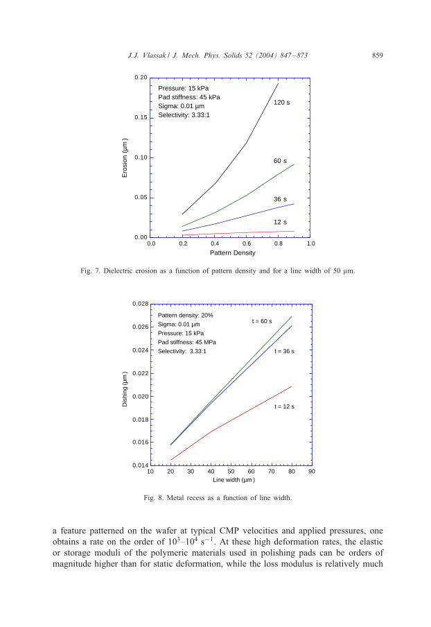
is clearly very sensitive to pattern density and increases with increasing polish time.This is also observed experimentally (Steigerwald et al., 1997). The e2ect of linewidth on dishing is shown in Fig. 8. According to the model, steady-state dishing ofmetal lines increases linearly with line width in agreement with experimental results(Steigerwald et al., 1997). It should be noted, however, that the model is valid only forfeatures wide enough that pad asperities can enter the recessed areas. This explains the4nite amount of dishing in the limit of zero line width, which is clearly not realistic.The interaction of asperities with the edges of features patterned on the wafer surfaceand the e2ect on the surface pro4le will be explored in more detail in the next section.

J.J. Vlassak / J. Mech. Phys. Solids 52 (2004) 847–873 857
-0.18
-0.16
-0.14
-0.12
-0.10
-0.08
-0.06
0 20 40 60 80 100
Pro
file
(µm
)
Distance (µm)
5 GPa
10
20
35
45
Polish time: 1 min
Removal rate: 300 nm/min
sigma: 0.01 µm
Pressure: 15 kPa
Selectivity: 3.33:1
0.010
0.015
0.020
0.025
0.030
0.035
0.040
0 0.05 0.1 0.15 0.2 0.25
Dis
hing
(µm
)
1/Pad stiffness (GPa- 1)
Line width: 20 µm
Line space: 80 µm
sigma: 0.01 µm
Pressure: 15 kPa
Selectivity: 3.33:1 0.6 - 2 min polish
0.2 min polish
(a)
(b)
Fig. 5. (a) Surface evolution for a metal line embedded in a dielectric as a function of pad sti2ness. Themetal removal rate is 300 nm=min. (b) Metal recess as a function of pad compliance for various polishtimes.
The model described in the previous section can also be applied at the lengthscale of the slurry particles. The abrasive particles in the polishing slurry are typi-cally much smaller than the asperities on the pad. Thus, at this length scale one canmodel the pad as a smooth half-space, while the abrasive particles take the role of as-perities. The force transmitted by an individual particle of diameter z is still given byEq. (3), while the average pressure between wafer and pad follows from Eq. (4), where

858 J.J. Vlassak / J. Mech. Phys. Solids 52 (2004) 847–873
0.000
0.020
0.040
0.060
0.080
0.100
0.120
0 0.02 0.04 0.06 0.08 0.1 0.12 0.14 0.16
Dis
hing
(µm
)
Sigma (µm)
t = 60 s
t = 36 s
t = 12 s
Pad stiffness: 45 MPa
Pressure: 15 kPa
Selectivity: 3.33:1
Line spacing: 80 µm
Line width: 20 µm
Steady state
0.002
0.004
0.006
0.008
0.010
0.012
0.014
0.016
0 0.02 0.04 0.06 0.08 0.1 0.12 0.14 0.16
Ero
sion
(µm
)
Sigma (µm)
t = 12 s
t = 36 s
t = 60 s
Line width: 20 µm
Line spacing: 80 µm
Selectivity: 3.33:1
Pad stiffness: 45 MPa
Pressure: 15 kPa
(a)
(b)
Fig. 6. (a) Dishing of a metal line embedded in a dielectric as a function of �. The metal removal rate is300 nm=min. (b) Dielectric erosion as a function of � for a metal line embedded in a dielectric.
now the distribution function for the particle diameter is used. If this distribution canbe approximated with an exponential function, Eq. (5) is obtained. This approach,however, presupposes that the curvature of the particles is independent of particle size.This is clearly not true for spherical particles, but may not be a bad approximation ifthe particles are irregular in shape.Thus far, it has been assumed that the pad is linearly elastic and that there are no
viscoelastic e2ects. If one calculates the strain rate of an asperity that is swept over
J.J. Vlassak / J. Mech. Phys. Solids 52 (2004) 847–873 859
0.00
0.05
0.10
0.15
0.20
0.0 0.2 0.4 0.6 0.8 1.0
Ero
sion
(µm
)
Pattern Density
Pressure: 15 kPa Pad stiffness: 45 kPaSigma: 0.01 µm Selectivity: 3.33:1
12 s
36 s
60 s
120 s
Fig. 7. Dielectric erosion as a function of pattern density and for a line width of 50 �m.
0.014
0.016
0.018
0.020
0.022
0.024
0.026
0.028
10 20 30 40 50 60 70 80 90
Dis
hing
(µm
)
Line width (µm )
t = 60 s
t = 36 s
t = 12 s
Pattern density: 20%
Sigma: 0.01 µm
Pressure: 15 kPa
Pad stiffness: 45 MPa
Selectivity: 3.33:1
Fig. 8. Metal recess as a function of line width.
a feature patterned on the wafer at typical CMP velocities and applied pressures, oneobtains a rate on the order of 103–104 s−1. At these high deformation rates, the elasticor storage moduli of the polymeric materials used in polishing pads can be orders ofmagnitude higher than for static deformation, while the loss modulus is relatively much

860 J.J. Vlassak / J. Mech. Phys. Solids 52 (2004) 847–873
less important. Thus, an asperity that is compressed as it is swept across a wafer, willstill deform elastically, but will not expand nearly as much into recessed areas as itwould at lower deformation rates. The result is a much sharper drop in pressure inrecessed areas than one would assume based on Eq. (5) using the static modulus. Ifthe relief on the wafer is of the same order of magnitude as the compression of theasperities, Eq. (5) can be used for the viscoelastic case as long as the high-frequencyelastic modulus is used. If, as is more likely, the relief is signi4cantly less than thetotal asperity compression, Eq. (5) can be linearized to calculate the change in pressureQp due to a change in gap between wafer and pad:
Qp(x; y; t) =−√���
2√�
(E
1− �2
)dyn
exp(− d(t)
�
)Qd(x; y; t); (13)
where the subscript “dyn” refers to the dynamic elastic modulus for the appropriatestrain rate. The factor Qd(x; y; t) in this expression represents the di2erence betweenthe actual gap between wafer and pad and the average gap d(t) for a given appliedpressure. Dynamic e2ects will result in an elevated pressure on protruding features anda reduced pressure on recessed features. Hence, dynamic e2ects may indeed play animportant role in the planarization of dielectrics as suggested by Yu et al. (1993).
4. Asperity shielding
In this section, the interaction of pad asperities with the edges of features patternedon a wafer surface is further explored. As shown in Fig. 8, the model discussed in theprevious sections predicts a 4nite metal line recess in the limit of zero line width. Thisis a direct result of the assumption that pad asperities behave like Hertzian contactsnear the edge of a feature. To illustrate that this is not the case, consider the contactof an asperity with a step pro4le as shown in Fig. 9. As the asperity moves fromleft to right, it 4rst contacts the raised portion of the step. When the asperity movesover the edge and touches the lower section of the pro4le, a second contact area isformed. Eventually, the asperity loses contact with the raised portion of the step. Thesolution of this contact problem in two dimensions is derived in Appendix A usingMuskhelishvili’s approach as discussed by Gladwell (1980). Fig. 10 depicts the pressuredistributions between the asperity and the surface of the wafer when it is centered on
Asperity
MetalOxide
Asperity
MetalOxide
Asperity
MetalOxide
Asperity
MetalOxide
Fig. 9. Interaction of an asperity with a step in the wafer surface.

J.J. Vlassak / J. Mech. Phys. Solids 52 (2004) 847–873 861
0
0.5
1
1.5
2
-1 -0.5 0 0.5 1 1.5
Normalized pressure
Nor
mal
ized
pre
ssur
e
Normalized position (x/a)
λ = 0
−−( )2 1 2pR
aE
ν
No contact
0
0.5
1
1.5
2
-1 -0.5 0 0.5 1 1.5
Nor
mal
ized
pre
ssur
eNormalized position x/a
λ = 0PN = 0.42
Normalized pressure
−−( )2 1 2pR
aE
ν
(a) (b)
Fig. 10. Pressure distribution for an asperity on a step. (a) One contact area; (b) two contact areas. Notethat a is negative.
the step. In the region where the asperity contacts the edge, a pressure singularity isformed, resulting in an in4nite removal rate at the step. The recessed area, on the otherhand, is shielded from contact with the asperity and the local pressure vanishes. Theremoval rate in this shielded area is reduced to zero. This analysis clearly indicates thatit is impossible for a discontinuous step to form within the context of this model. Anystep that forms as a result of a discontinuity in wear coeJcient, would be removedimmediately. This in turn implies that the pressure cannot be continuous across aboundary between two materials with di2erent wear coeJcients. According to Eq.(10), the ratio of the average pressure on either side of the boundary must be equalto the selectivity to ensure an equal removal rate for both materials and to keep astep from forming. The resulting contact can therefore not be described as a simpleHertzian contact.In order to assess the e2ect of this non-Hertzian contact of asperities near boundaries
between two materials, a simple two-dimensional model is proposed. Consider a pro4leS(x; t) at time t with a discontinuity in the wear coeJcient at the origin as shown inFig. 11. As asperities sweep the surface of the wafer, an average pressure distributionTp(x; t) develops between wafer and pad. The average pressure at x can be calculatedfrom the pressure distribution between the wafer and an individual asperity:
Tp(x; t) =1
a1 + a2
∫ x+a1
x−a2p(x; !; t) d!; (14)
where p(x; !; t) is the pressure distribution between an asperity with centerline at !,and where ! − a1 and ! + a2, respectively, represent the left- and rightmost lines ofcontact between the asperity and the wafer, as shown in Fig. 11. Thus, in order tocalculate the average pressure distribution, p(x; !; t) needs to be determined 4rst. Thepressure distribution for an asperity with radius of curvature R and with center line at

862 J.J. Vlassak / J. Mech. Phys. Solids 52 (2004) 847–873
21
x
z
k1 k2
λa1 a2
S(x,t)
Fig. 11. Contact of an asperity with wafer surface. At the origin the wear coeJcient changes from k1 to k2.
! on a surface S(x; t) must obey the equation (Johnson, 1985)
− 21− �2
�E
∫ !+a2
!−a1p(s; !; t) ln|x − s| ds= S(x; t) +
(x − !)2
2R+ C; (15)
for !− a1 ¡x¡!+ a2, where C is an integration constant. In addition, the followingconditions need to be satis4ed
P =∫ !+a2
!−a1p(x; !; t) dx; (16)
p(0+; !; t)p(0−; !; t)
=k1k2; (17)
where k1 and k2 are the wear coeJcients for x¡ 0 and x¿ 0, respectively. Eq. (16)ensures that the load per unit length on the asperity is equal to P; the second equa-tion follows from the requirement that no step can develop at the origin. Eq. (17) issomewhat more limiting than is strictly necessary, since it is suJcient for the averagepressure to satisfy this equation. Finally, the evolution of the surface pro4le S(x; t) isrelated to the average pressure distribution Tp(x; t) through
@S(x; t)@t
=−kiv(x; t) Tp(x; t); (18)
where the subscript i takes on the values of 1 or 2 depending on the material. Eqs. (14)–(18) need to be solved numerically. The solution procedure is discussed in AppendixB. Selected results are presented in Figs. 12–16. Consider an initially Eat surface withk1 ¡k2. This would be the case for a damascene process where the material left of theorigin is a dielectric and the material to the right a metal. Fig. 12 shows the pressuredistribution underneath an asperity centered at the origin, where the wear coeJcient

J.J. Vlassak / J. Mech. Phys. Solids 52 (2004) 847–873 863
0
0.5
1
1.5
2
2.5
3
3.5
4
-1.5 -1 -0.5 0 0.5 1 1.5
Normalized position
Nor
mal
ized
pos
ition
Polish time: 5 sRemoval rate: 300 nm/minSelectivity: 10:1Step height is 23.4 nmDown force: 4.67 N/mR: 30 µm E/(1-ν2): 45 MPa
Hertzian contact
Step profile
Actual
p-
p+
Fig. 12. Pressure distribution for an asperity centered at the origin. The dashed lines show the pressure pro4lesfor a discrete step and for a Hertzian contact. The step height was determined as the height di2erence overthe total contact length. The x coordinate is normalized with the Hertzian contact length; the pressure isnormalized with the maximum Hertzian contact pressure. The metal removal rate is 300 nm=min at a pressureof 15 kPa.
changes abruptly from k1 to k2. The dashed lines show the pressure pro4les for adiscrete step and for a Hertzian contact. The pressure pro4le closely approaches thatfor a discrete step suJciently far away from the origin. Near the origin, it is boundedby the pressure distribution for a Hertzian contact and that for a discreet step. Fig. 13depicts how the pressure distribution underneath an asperity evolves during the CMPprocess. With increased polish time, a larger fraction of the load is supported by thedielectric, which increasingly shields the metal area. Fig. 14 illustrates the evolution ofan initially Eat surface as a function of time assuming a constant load is applied to theasperity. As time progresses, the area with the higher removal rate becomes increasinglymore recessed, while the shielding e2ect of the edge is felt over a longer distance. Thee2ect of selectivity is depicted in Fig. 15. In this 4gure, the vertical dimension hasbeen shifted and normalized to ensure that the degree of recess is identical for eachcurve. The selectivity has a signi4cant e2ect on the degree of erosion of the dielectricand hence on the surface pro4le: as the selectivity increases a more pronounced corneris formed. The e2ect of applied pressure is illustrated in Fig. 16, which depicts thepro4les that are formed when two di2erent loads are applied to the asperity. Polishtimes have been adjusted to result in the same overall amount of metal removed andthe resulting pro4les have been normalized. Despite the di2erence in contact length−1:99 versus 1:58 �m—the normalized pro4les are virtually identical. This indicates

864 J.J. Vlassak / J. Mech. Phys. Solids 52 (2004) 847–873
0
0.5
1
1.5
2
2.5
3
3.5
-1.5 -1 -0.5 0 0.5 1 1.5
Nor
mal
ized
pre
ssur
e
Normalized x-coordinate
6.2 s polish
1.2 s
1.2 s polish
6.2 s
Removal rate: 300 nm/min
Selectivity: 10:1
Down force: 4.67 N/m
R: 30 µ m
E/(1-ν2) = 45 MPa
0
Fig. 13. Evolution of the pressure distribution p(x; t) for an asperity centered at the origin as a function ofpolish time. Curves are for 1 s time increments. The x coordinate is normalized with the Hertzian contactlength; the pressure is normalized with the maximum Hertzian contact pressure.
-35
-30
-25
-20
-15
-10
-5
0
-3 -2 -1 0 1 2 3
Sur
face
pro
file
(µm
)
x-coordinate (µm )
2.2 seconds
6.2 seconds
Etch rate: 5 nm/s
Selectivity: 2:1
Down force: 4.67 N/m
R: 30 µ m
E/(1-ν2 ) = 45 GPa
Fig. 14. Evolution of the surface pro4le as a function of polish time. Curves are for one second timeincrements.

J.J. Vlassak / J. Mech. Phys. Solids 52 (2004) 847–873 865
-1.2
-1
-0.8
-0.6
-0.4
-0.2
0
0.2
-1.5 -1 -0.5 0 0.5 1 1.5
Selectivity: 4:3
Selectivity: 2:1
Selectivity: 4:1
Selectivity: 10:1
Normalized distance x/a
Nor
mal
ized
pro
file
c
P/ER = 3.46 10-3
Etch time: 5.2 secEtch rate: 5 nm/sec
ac= 1.99 µmSelectivity: 10:1
Selectivity: 4:3
Fig. 15. Surface pro4le for various values of CMP selectivity. The x coordinate is normalized with theHertzian contact length; pro4les have been shifted and normalized to make the nominal amount of oxideremoved equal to zero and the amount of metal equal to one.
that the shape of the pro4le is mainly determined by the absolute step height goingfrom one material to another rather than the contact length.Instead of applying a constant load as the asperity slides across the wafer, it is also
possible to couple the pad roughness model presented in Section 2 with the asperityshielding model discussed in this section. This can be achieved by using the pres-sure distribution obtained from the roughness model to determine the interaction ofthe asperities with the edges of features patterned on a wafer. To ensure that the con-tact pressure for the two-dimensional asperities in the asperity shielding model is thesame as for three-dimensional asperities, the line load applied to the two-dimensionalasperities must be equal to
P =643�3
3
√4p2E
3�2R(1− �2); (19)
where p is the pressure distribution obtained from the pad roughness model. It is clearfrom Eq. (19) that P depends on both asperity density and curvature, although the e2ectof these quantities on the 4nal pro4le is expected to be rather weak given the resultsin Fig. 16. Since the asperity shielding model is essentially a two-dimensional model,the model is necessarily be qualitative. The extension to a three-dimensional asperityshielding model is straightforward but computationally expensive. Such a model wouldgive a much improved description of metal recess as a function of line width in the

866 J.J. Vlassak / J. Mech. Phys. Solids 52 (2004) 847–873
-1.2
-1
-0.8
-0.6
-0.4
-0.2
0
0.2
-3 -2 -1 0 1 2 3
Etch time: 3 secondsDown force: 2.34 N/m
Etch time: 6 secondsDown force: 4.67 N/m
x-coordinate (µm)
No
rma
lize
d p
rofile
Etch rate: 5 nm/s
Selectivity: 10:1
R: 30 µm
Fig. 16. Surface pro4le for various values of down force applied to an asperity. Polish times have beenadjusted to result in the same overall amount of metal removed. Pro4les have been shifted and normalizedto make the nominal amount of oxide removed equal to zero and the amount of metal equal to one.
limit of very narrow lines. It should be noted that the asperity shielding model currentlydoes not use a statistical description of the asperity height.
5. Conclusions
The chemical mechanical polishing process is analyzed using a model based on con-tact mechanics. The model takes into account the compliance of the polishing padas well as its roughness. It can be applied to metal damascene, shallow trench iso-lation, and dielectric planarization. Contact mechanics and a statistical description ofpad roughness are used to calculate the pressure distribution between wafer and polish-ing pad and to predict the evolution of the wafer surface pro4le during the polishingprocess. The model successfully predicts experimentally observed trends reported inthe literature. According to the model, pad roughness enhances dishing of metal linessigni4cantly, but has only a limited e2ect on dielectric erosion. As features on thewafer become increasingly narrow, asperity shielding becomes important. A simplenon-Hertzian contact model is proposed to take asperity shielding into account. Thismodel ensures that no steps are formed on the wafer surface and can be readily inte-grated with the pad roughness model.

J.J. Vlassak / J. Mech. Phys. Solids 52 (2004) 847–873 867
x
z
a b c λ0
h
Fig. 17. Schematic representation of the contact of a cylindrical asperity with a step of height h.
Acknowledgements
The author gratefully acknowledges 4nancial support from the Division of Engineer-ing and Applied Sciences at Harvard University.
Appendix A. A cylindrical asperity on a step
Consider the contact of a two-dimensional asperity with a step pro4le as shown inFig. 17. Let ! be the distance from the center line of the asperity to the step, takennegative when the asperity is to the left of the step and positive otherwise. Let &represent the contact area between the asperity and the step pro4le and R the radiusof curvature of the asperity. The contact of an asperity with a step of height h at theorigin, can then be described mathematically as follows:
w(x)
{='+ f(x) for x∈&;
¿'+ f(x) for x �∈ &;p(x)
{¿ 0 for x∈&;
=0 for x �∈ &;(A.1)
where ' represents the far-4eld displacement, w(x) is the vertical displacement ofthe surface of the asperity, and f(x) is the gap between the two surfaces beforedeformation, given by
f(x) =
− (x − !)2
2Rfor x6 0;
− (x − !)2
2R− h for x¿ 0:
(A.2)
The solution of this contact problem can be described in terms of a complex potential((z) such that (Gladwell, 1980):
(+(x) + (−(x) =2E
1− �2iw′(x) =
2E1− �2
if′(x) for x∈&;
(−(x)− (+(x) = p(x) = 0 for x �∈ &;(A.3)

868 J.J. Vlassak / J. Mech. Phys. Solids 52 (2004) 847–873
where z = x + iy. This set of two linear equations is satis4ed if
2(1− �2)E
((z) =)0(z)2�
∫&
f′(t) dt)+0 (t)(t − z)
+ )0(z)(c1z + c0): (A.4)
If the asperity contacts the upper part of the step from point a to the origin, and thelower part from b to c, the function )0(z) is de4ned as
)0(z) =1√
(z − a)(z − b)(z − c): (A.5)
The constant c1 in Eq. (A.4) is determined from the total load per unit length, P,applied to the asperity
c1 =−1− �2
�EiP; (A.6)
while c0 follows from the step height
f(b)− f(0) =∫ b
0w′(x) dx =−h−
((b− !)2
2R− !2
2R
): (A.7)
The points a; b, and c are determined from the requirement that the pressure shouldvanish at the edges of the contact:
p(a) = p(b) = p(c) = 0: (A.8)
The integral in Eq. (A.4) can be calculated analytically for f(x) given by Eq. (A.2)and one 4nds
2(1− �2)E
((z) =i2R
[)0(z)S(z; !)− (z − !)] + )0(z)(c1z + c0); (A.9)
where S(z; !) is a simple cubic polynomial in z:
S(z; !) = z3 − 12 z
2(a+ b+ c + 2!)
+18 z(2ab+ 2ac + 2bc − a2 − b2 − c2 + 4a!+ 4b!+ 4c!)
− 116 (a
3 + b3 + c3 − a2b− ab2 − b2c − bc2 − a2c − ac2 + abc)
+18 !(a
2 + b2 + c2 − 2ab− 2ac − 2bc): (A.10)

J.J. Vlassak / J. Mech. Phys. Solids 52 (2004) 847–873 869
The pressure distribution in the contact area can be derived from Eqs. (A.9) and (A.3).The conditions in Eq. (A.8) can then be expressed as a set of three cubic equations
S(a; !)− 2RP(1− �2)�E
a− 2ic0R= 0;
S(b; !)− 2RP(1− �2)�E
b− 2ic0R= 0;
S(c; !)− 2RP(1− �2)�E
c − 2ic0R= 0: (A.11)
The solution of this set of equations is remarkably simple:
ba=
12
(−1 + 2
!a+
√8PN + 4
!a− 3
);
ca=
12
(−1 + 2
!a−√8PN + 4
!a− 3
); (A.12)
PN + HN =12− !
a+
12
(!a
)2;
where
PN =2R(1− �2)P
�a2E;
HN =2ic0Ra3
; (A.13)
are dimensionless constants related to the applied load and step height, respectively.Eqs. (A.12), (A.13), and (A.7) represent a parametric solution to the contact problem.For a given value of a and applied load P, the values of b and c can be calculated fromEq. (A.12) and (A.13). The step height, h, corresponding to this particular solution thenfollows directly from Eqs. (A.13) and (A.7). The only numerical step involved is theevaluation of the integral in Eq. (A.7). Fig. 18 shows the normalized step height as afunction of HN for several values of !.
The conditions for 4rst contact with the recessed portion of the step are
a=23
(!−
√!2 +
12PR(1− �2)�E
); b= c = !− 1
2a; (A.14)
hRa2
=−18
[2!a
√3 + 4
(!a− 2)
!a+(4!a− 3)
× ln
(2− 2
!a+
√3 + 4
(!a− 2)
!a
)]: (A.15)

870 J.J. Vlassak / J. Mech. Phys. Solids 52 (2004) 847–873
0
0.2
0.4
0.6
0.8
1
0 0.2 0.4 0.6 0.8 1
λ/a = 0.45
λ/a = 0
λ/a = -1
λ/a = -5
λ/a = -20Nor
mal
ized
ste
p he
ight
(hR
/a2 )
/(hR
/a2 )
ma
x
HN/HNmax
HaN
max = −18
1 22λ
Fig. 18. Normalized step height as a function of HN for several values of !. HN and (hR=a) have beennormalized by the corresponding values for the limiting case where the asperity 4rst contacts the recessedarea: (hR=a)max is given by Eq. (A.15), the expression for Hmax
N is given in the 4gure.
As before, it is much easier to calculate the step height as a function of applied loadthan to solve these equations for the applied load given the step height. Note that band c coincide at the point of 4rst contact with the recessed part of the step. Hence, noload is transferred between the asperity and the recessed area. The expression for a inEq. (A.14) therefore also holds even when the asperity does not contact the recessedarea and in e2ect represents the solution for an asperity on an in4nite step.Taking into account Eqs. (A.11), (A.3), and (A.9), the pressure distribution under
the asperity can be written as
p(x) =E
2R(1− �2)
√(a− x)(b− x)(c − x)
x
for a¡x¡ 0 or b¡x¡c; (A.16)
if there are two contact areas. If the asperity contacts only the raised part of the step,the pressure distribution is found to be
p(x) =E
2R(1− �2)
√a− xx
(!− 1
2a− x
)for a¡x¡ 0: (A.17)
Appendix B. Numerical solution of the asperity shielding problem
The equations describing the asperity shielding model need to be solved numerically.The main diJculty lies in solving the integral equation in Eq. (15) for an arbitrary

J.J. Vlassak / J. Mech. Phys. Solids 52 (2004) 847–873 871
p
x
p-
p+
d d
Fig. 19. Schematic representation of the traction element used at the origin where there is a discontinuity inwear coeJcient.
pro4le S(x; t). The approach taken here consists of replacing the pressure distributionin Eq. (15), p(s; !; t), with a piecewise-linear distribution of tractions built up by thesuperposition of overlapping triangular traction elements (Johnson, 1985). The tractiondistribution is then speci4ed completely by the discrete values pj of the traction ele-ments, which are determined using the collocation method. Eq. (15) is then replacedby a set of linear equations in pj that can be easily solved. The coeJcients of theunknown pj in this set of equations are called the inEuence coeJcients and they aregiven by Johnson (1985) for a triangular pressure distribution. Since the pressure dis-tribution is discontinuous at the origin where the wear coeJcient changes abruptly, aspecial traction element needs to be used there. Fig. 19 illustrates the pressure elementused at the origin. The corresponding inEuence coeJcient is easily derived from thefollowing expression for the deEection u due to the pressure distribution depicted inFig. 19
u(x) =− (1− �2)d�E
[(−dx + (d+ x)2 ln
∣∣∣∣d+ xx
∣∣∣∣+ d2 ln|x|)p−
+(dx + (d− x)2 ln
∣∣∣∣d− xx
∣∣∣∣+ d2 ln|x|)p+]; (B.1)
where d; p− and p+ are de4ned in Fig. 19. In case p− = p+, Eq. (B.1) reduces tothe result for an element with a continuous triangular pressure distribution. Since theelement at the origin involves two discreet values for pressure, an additional equationlinking both values is needed. The relationship between p− and p+ follows fromEq. (17):
k1p− = p+k2: (B.2)
The unknown integration constant C in Eq. (15) can be eliminated from the equationsby considering displacements relative to a given point, e.g., the point of 4rst contact.The pressure at the point of 4rst contact then cannot be determined from the set oflinear equations derived from Eq. (15), but Eq. (16) for the total load provides themissing equation.

872 J.J. Vlassak / J. Mech. Phys. Solids 52 (2004) 847–873
An additional diJculty arises from the fact that the contact area between wafer andasperity is not known a priori and an iterative scheme needs to be adopted to solvethe contact problem. Initially the contact area is assumed to be slightly larger than theHertzian contact area. If the values of pj near the edge of the contact are negative,the contact area is too large and a tensile traction is required to maintain contact overthe entire assumed area. Elements that yield a negative pressure are excluded from thenext iteration and the pressure for these elements is taken to be zero. This procedureconverges quickly to a set of non-negative values of pj, which represent the pressuredistribution for the contact problem. The size of the contact area then determines a1and a2.
This procedure is used to calculate the pressure distribution between an asperity andthe wafer as the asperity is swept across the wafer. The average pressure at a point x isthen calculated from Eq. (14) by integrating the pressure distribution as ! varies fromx−a2 to x+a1. Once the average pressure distribution is known, Eq. (18) is integratedto determine the evolution of the pro4le S(x; t). This integration is performed using thebackward Euler technique to ensure stability of the procedure. The results presented inFigs. 12–16 were obtained by discretizing a 40 �m section of the wafer surface using400 elements. The time step for integrating Eq. (18) was 0:2 s.
References
Boning, D., Lee, B., Oji, C., Ouma, D., Park, T., Smith, T., Tugbawa, T., 1999. Pattern dependent modelingfor CMP optimization and control. In: Babu, S.V., Danyluk, S., Krishnan, M., Tsujimura, M. (Eds.),Chemical–Mechanical Polishing–Fundamentals and Challenges. Proceedings of the Materials ResearchSociety, San Francisco, pp. 197–209.
Chekina, O.G., Keer, L.M., Liang, H., 1998. Wear-contact problems and modeling of chemical mechanicalpolishing. J. Electrochem. Soc. 145 (6), 2100–2106.
Cook, L.M., 1990. Chemical processes in glass polishing. J. Non-Cryst. Solids 120, 152–171.Elbel, N., Neureither, B., Eberberger, B., Lahnor, P., 1998. Tungsten chemical mechanical polishing. J.
Electrochem. Soc. 145 (5), 1659–1664.Gladwell, G.M.L., 1980. Contact Problems in the Classical Theory of Elasticity. Sijtho2 & Noordho2, Alphen
aan den Rijn, The Netherlands.Gradshtein, I.S., Ryzhik, I.M., 1994. Tables of Integrals, Series, and Products. Academic Press, New York,
London.Greenwood, J.A., Tripp, J.H., 1967. The elastic contact of rough spheres. J. Appl. Mech. 34, 153–159.Greenwood, J.A., Williamson, J.B., 1966. Contact of nominally Eat surfaces. Proc. Roy. Soc. A 295,
300–319.Johnson, K.L., 1985. Contact Mechanics. Cambridge University Press, Cambridge, MA.Kaufman, F.B., Thompson, D.B., Broadie, R.E., Jaso, M.A., Guthrie, W.L., Pearson, D.J., Small, M.B.,
1991. Chemical–mechanical polishing for fabricating patterned W metal features as chip interconnects. J.Electrochem. Soc. 138 (11), 3460–3465.
Onions, R.A., Archard, J.F., 1973. Contact of surfaces having a random structure. J. Phys. D 6 (3),289–304.
Runnels, S.R., 1994. Feature-scale Euid-based erosion model for chemical–mechanical polishing. J.Electrochem. Soc. 141 (7), 1900–1904.
Shan, L., Danyluk, S., Levert, J.A., 1999. Interfacial pressure measurements at chemical mechanical polishinginterfaces. In: Babu, S.V., Danyluk, S., Krishnan, M., Tsujimura, M. (Eds.), Chemical–MechanicalPolishing—Fundamentals and Challenges. Proceedings of the Materials Research Society, San Francisco,pp. 187–195.

J.J. Vlassak / J. Mech. Phys. Solids 52 (2004) 847–873 873
Steigerwald, J.M., Murarka, S.P., Gutmann, R.J., 1997. Chemical Mechanical Planarization of MicroelectronicMaterials. Wiley, New York.
Sundararajan, S., Thakurta, D.G., Schwendeman, D.W., Murarka, S.P., Gill, W.N., 1999. Two-dimensionalwafer-scale chemical mechanical planarization models based on lubrication theory and mass transport. J.Electrochem. Soc. 146 (2), 761–766.
Thakurta, D.G., Borst, C.L., Schwendeman, D.W., Gutmann, R.J., Gill, W.N., 2000. Pad porosity,compressibility and slurry delivery e2ects in chemical–mechanical planarization: modeling andexperiments. Thin Solid Films 366, 181–190.
Tichy, J., Levert, J.A., Shan, L., Danyluk, S., 1999. Contact mechanics and lubrication hydrodynamics ofchemical mechanical polishing. J. Electrochem. Soc. 146 (4), 1523–1528.
Tseng, W.-T., Wang, Y.-L., 1997. Re-examination of pressure and speed dependencies of removal rate duringchemical mechanical polishing processes. J. Electrochem. Soc. 144 (2), L14.
Warnock, J., 1991. A two-dimensional process model for chemimechanical polish planarization. J.Electrochem. Soc. 138 (8), 2398–2402.
Yu, T.-K., Yu, C.C., Orlowski, M., 1993. A statistical polishing pad model for chemical–mechanicalpolishing. International Electron Devices Meeting, Proceedings of the IEEE 35.4.1–4.