agilent pn 89400-8 using vector modulation analysis in the...
TRANSCRIPT

IntroductionThe Agilent Technologies 89400 Series vector signal analyzers (VSAs) with vector modulation analysis (Option AYA) provide the numerical and visualtools to help quickly identify and quantify impairments to digitally modulatedsignals, whether using standard or several nonstandard modulation formats.Measurements are possible on continuous or burst carriers (such as TDMA) at baseband, IF, and RF locations throughout a system block diagram. There is no need for external filtering, coherent carrier signals, or symbol clock tint-ing signals. The 89400 Series VSAs with Option AYA have built-in Gaussian,raised-cosine, root-raised-cosine, and user-definable filters (with adjustablealpha or BT) and lock to the carrier and a defined symbol rate.
Although it is useful to measure the signal being transmitted, imagine the ben-efit of being able to detect, quantify, and locate the errors in the transmittedsignal when compared to an ideal reference signal. Common vector modulationanalysis tools such as eye and constellation displays are supported as well asnew analysis tools including the ability to compare measured signals to idealsignals. Measurements update as fast as two times per second, allowing theeffects of changes to an active system to be quickly analyzed. Advanced spec-trum analysis rounds out the 89400 Series VSAs’ measurement contributions(additional information is in the reference list). By reducing the amount ofexternal equipment or the need for developing custom solutions, accuracy ispreserved and system development time can be simplified and minimized.
Basic vector modulation and measurement concepts are presented, followed byexample measurements and setups. A transmitter system is used as the foun-dation for the measuements; however, any system with I and Q signals can usethe principles and tools presented. These applications are intended to serve as examples of the measurement power and ease of use of the analyzer.
Agilent PN 89400-8
Using Vector Modulation Analysis in theIntegration, Troubleshooting, and Design ofDigital RF Communications SystemsProduct Note

2
12348
9
15202021
212223242728
Contents
IntroductionBackgroundModulation conceptsMeasurement conceptsProblems that can occur during transmission, integration, and designIdentifying problems: Using measurements and display toolsSetting up the measurementsGenerating digitally modulated signalsCreating the arbitrary sourceMeasuring a signal (using the arbitrary source)Other toolsSummaryConfiguration guideGlossaryReferencesIndex
BackgroundModulation is a method of carryinginformation from a transmitter to oneor more receivers. Communicationsystems use modulation to superim-pose or “piggyback” low-frequencyvoice or data signals onto an RF wave(high-frequency carrier) which can betransmitted long distances. The infor-mation (voice or data) is used tomodulate the carrier, usually by alter-ing its phase, frequency, amplitude,or some combination of these. Thereceiver extracts or decodes the mod-ulation from the incoming signal torecover the desired information.
Due to the propagation characteristicsof electromagnetic waves with differentfrequencies, certain portions of thespectrum are more desirable for someapplications. With the applicationsexplosion in consumer communica-tions, a desire for direct and reliabletransmission of digital information,and a drive for improved quality and
privacy, there has been increased needfor more efficient and smarter use ofthe already crowded RF frequencyspectrum. Digital modulation hasbeen used for many years, however,now it is being used more widely toaddress the aforementioned needs ina variety of applications. Digital (alsocalled complex or IQ) modulationuses a combination of amplitude andphase modulation.
Many digital modulation communica-tions schemes make better use of theavailable spectrum by allowing multi-ple users per carrier frequency (i.e., toaccess the same portion of spectrum)and take advantage of compressiongains in digital signal processing (DSP)portions of the systems. Time-divisionmultiple access (TDMA) is one methodof spectrum sharing. It uses burstcarriers which only transmit for shortperiods and are off while other usersoccupy the channel. A second methodof sharing is to combine the desired
signal with a code sequence thatresults in spread spectrum or code-division multiple access (CDMA) sig-nals. CDMA signals simultaneouslyoccupy the same spectrum and affecteach other like broadband noise.
Figure 1 shows the basic block dia-gram of a digital RF communicationssystem, which could be the core ofpersonal communications systems,cordless telephones, digital specialservices systems, cellular telephones,pagers, wireless LANs, private trunkedmobile systems, satellite communica-tions services, global positioning, digi-tal audio broadcast, fleet dispatchingnetworks, digital video, and radarsystems. Developing, testing, integrat-ing, and troubleshooting these newsystems requires flexible testingcapabilities to locate the probablecauses of any signal degradation. In many cases, modulation formatsthat are not standardized are used.

3
Modulation conceptsIn most digital radio systems, the frequency of the carrier is fixed soonly phase and magnitude need to beconsidered. The phase and magnitudecan be represented in polar or vectorcoordinates as a discrete point in the I-Q plane (Figure 2). I representsin-phase (phase reference) and Q represents quadrature (90° out ofphase). By forcing the carrier to oneof several predetermined positions in
the I-Q plane, we can then transmitencoded information. Each positionor state (or transitions between thestates in some systems) represents acertain bit pattern that can be decodedat the receiver. The mapping of thestates at each symbol timing instant(when the receiver interprets the sig-nal) on the I-Q plane is referred to asa constellation diagram. Theoretically,there should be single points, but apractical system suffers from various
impairments and noise that cause aspreading of the states (a dispersal of dots around each state).
An example modulation format is 16QAM (16-state quadrature amplitudemodulation). This format takes fourbits of serial data and encodes themas single amplitude/phase states, orsymbols. A state diagram is shown inFigure 3. In order to generate this mod-ulation format, the I and Q carriers
Transmitter
A/DProcessing/Compression/Error Corr
EncodeSymbols
IQ
ISIIQ
Mod
IFReceiver
RF
AGC
IF IF
Demod
ISIIQ
IQ
DecodeBits D/A
RF
Digital Communications System
Figure 1. Many systems use this block diagram, including cellular radios, wireless LANs, fleet dispatch networks, and others.
Figure 2. Digital communications systemsuse the magnitude and phase of signals totransmit encoded information.
Figure 3. The binary representation for each state is user-definable in the Agilent89400 Series VSAs.
4
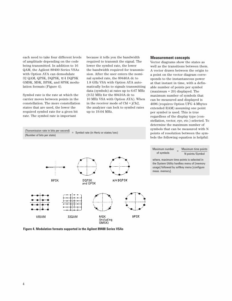
each need to take four different levelsof amplitude depending on the codebeing transmitted. In addition to 16QAM, the Agilent 89400 Series VSAswith Option AYA can demodulate 32 QAM, QPSK, DQPSK, π/4 DQPSKGMSK, MSK, BPSK, and 8PSK modu-lation formats (Figure 4).
Symbol rate is the rate at which thecarrier moves between points in theconstellation. The more constellationstates that are used, the lower therequired symbol rate for a given bitrate. The symbol rate is important
because it tells you the bandwidthrequired to transmit the signal. Thelower the symbol rate, the lower the bandwidth required for transmis-sion. After the user enters the nomi-nal symbol rate, the 89440A dc to 1.8 GHz VSA with Option AYA auto-matically locks to signals transmittingdata (symbols) at rates up to 6.67 MHz(9.52 MHz for the 89410A dc to 10 MHz VSA with Option AYA). Whenin the receiver mode of Chl + jCh2, the analyzer can lock to symbol ratesup to 19.04 MHz.
Measurement conceptsVector diagrams show the states aswell as the transitions between them.A vector drawn between the origin toa point on the vector diagram corre-sponds to the instantaneous power at that instant in time, with a defin-able number of points per symbol(maximum = 20) displayed. The maximum number of symbols thatcan be measured and displayed is4096 (requires Option UFG 4-Mbytesextended RAM) assuming one pointper symbol is used. This is trueregardless of the display type (con-stellation, vector, eye, etc.) selected. Todetermine the maximum number ofsymbols that can be measured with Npoints of resolution between the sym-bols the following equation is helpful:
Figure 4. Modulation formats supported in the Agilent 89400 Series VSAs
Maximum number=
Maximum time pointsof symbols N points/Symbol
where, maximum time points is selected in the System Utility hardkey menu of [memoryusage] followed by softkey menu [configuremeas. memory].
(Transmission rate in bits per second)= Symbol rate (in Hertz or states/sec)
(Number of bits per state)
5
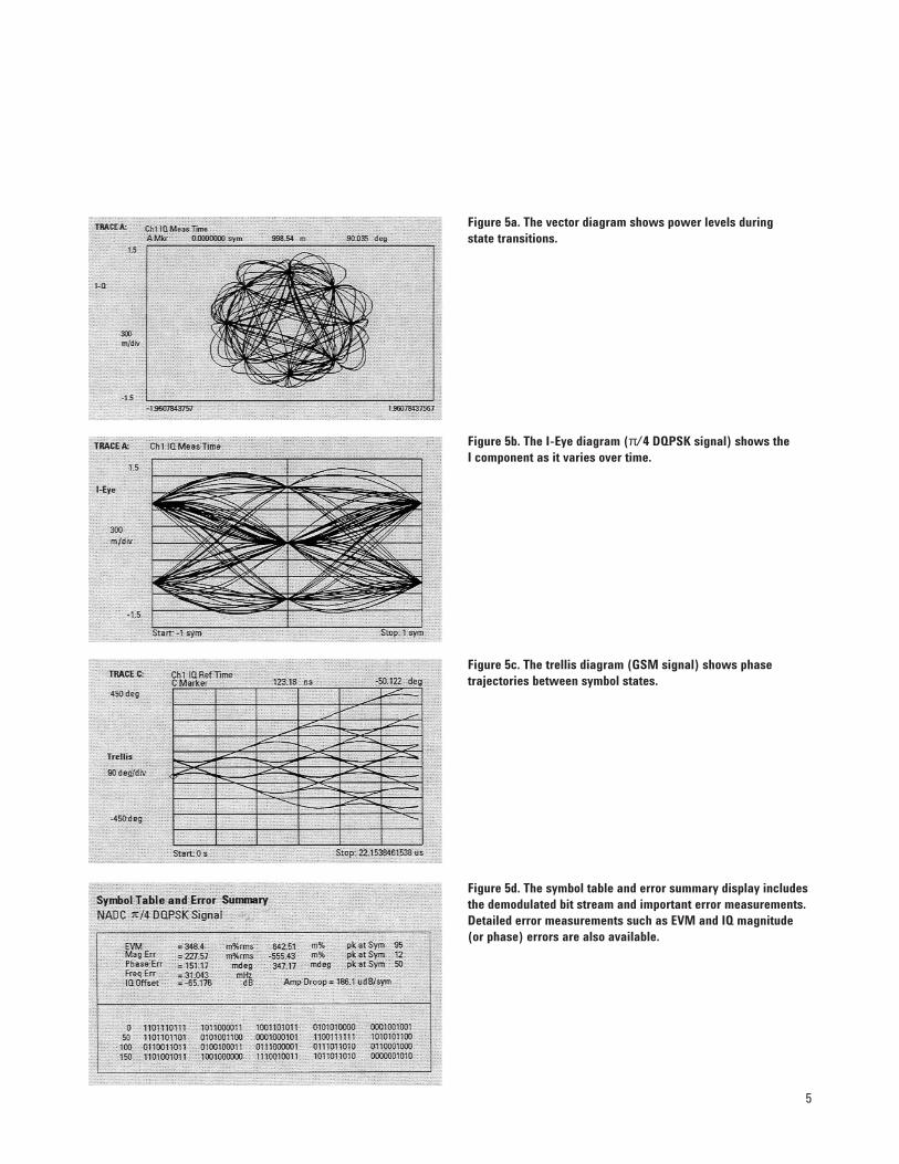
Figure 5a. The vector diagram shows power levels during state transitions.
Figure 5b. The I-Eye diagram (π/4 DQPSK signal) shows the I component as it varies over time.
Figure 5c. The trellis diagram (GSM signal) shows phase trajectories between symbol states.
Figure 5d. The symbol table and error summary display includesthe demodulated bit stream and important error measurements.Detailed error measurements such as EVM and IQ magnitude(or phase) errors are also available.
6
I and Q eye diagrams are anothercommon analysis display. These dia-grams are simply a mapping of I mag-nitude versus time and Q magnitudeversus time as these waveforms wouldappear on an oscilloscope which istriggered at the symbol timing instants.The 89400 Series VSAs with OptionAYA can display these as well as trellisdiagrams which map phase versustime (the phase trajectory per symbol)for the measured or the ideal (refer-ence) signal. MSK (minimum shift key)signals have constant amplitude butvary phase to transmit information.Trellis diagrams are often used tocharacterize these signals because oftheir ability to map phase transitionsand trajectories at each symbol. Eyeand trellis diagrams represent thesymbol clock detection points by thevertical lines displayed.
A symbol table shows the final productof the demodulation—the binary bits foreach symbol detected. Simultaneousmultiple display grids with theirmarkers coupled can compare the bit
pattern detected with the data’s posi-tion in the constellation, vector, or eyediagrams. When displaying the symboltable, a numerical error summary isalso listed which lists parameters suchas overall magnitude and phase error(and the peak error with its symbollocation), frequency error, amplitudedroop, origin (or IQ) offset, and errorvector magnitude (% rms and peak).
Detect, quantify, and locate the errorsin the transmitted signal by comparingit to an ideal reference signal. Theideal reference is the signal that wouldresult after demodulating your signalif it contained no errors. The genera-tion of an ideal reference signal isshown in Figure 17.
Error Vector MagnitudeThe 89400 Series VSAs with OptionAYA measure and display magnitudeand phase errors (IQ magnitude andIQ phase error) as well as the errorvector magnitude (EVM) at andbetween each state. A measure ofEVM (rms) is now included in NADC
and PDC specifications; however, it is also a useful means for quantifyingerrors for other digital modulationformats.
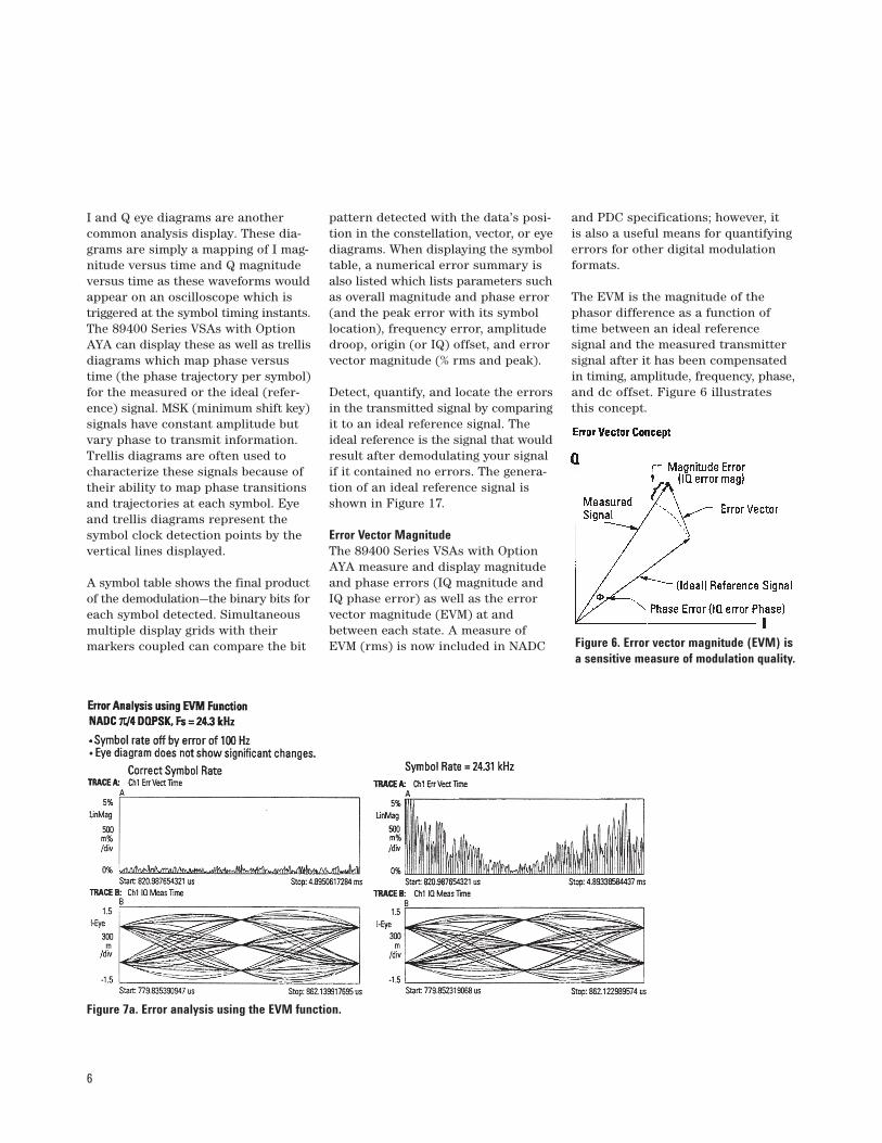
The EVM is the magnitude of the phasor difference as a function oftime between an ideal reference signal and the measured transmittersignal after it has been compensatedin timing, amplitude, frequency, phase,and dc offset. Figure 6 illustratesthis concept.
Figure 7a. Error analysis using the EVM function.
Figure 6. Error vector magnitude (EVM) isa sensitive measure of modulation quality.
7
The error vector magnitude (errorvector time) can detect errors in asignal’s transmission that may not beapparent using traditional analysisdisplays. As an example, Figure 7ashows an NADC signal with and with-out an error in the symbol rate used.Notice that the eye diagram is not ableto detect the error. Figure 7b illustratesan error that could not be detected byeither an eye or a constellation diagram.
Error vector spectrum is the spectrum/frequency domain representation oferror vector time. The center frequencyof this measurement’s display is typically the transmitter carrier frequency (refer to “Setting Up theMeasurements—Tune” on page 16).Traditionally, spurious signals thatare offset from the carrier weredetected using a constellation diagram.In these instances, the constellationmay show the states scattered in a
circle or crescent around each of theideal state locations. This is not nec-essarily the case for close-in spurs.Error vector spectrum can indicateand measure the frequency of spuri-ous signals which may be offset fromthe carriers that could not be observedon traditional spectrum analyzers orby using a constellation display. Anexample showing a spur that is offsetapproximately 7 kHz from the carrieris illustrated in Figure 8.
Error Analysis using EVM Function• NADC signal with wrong filter coefficient alpha=0.4 causes large errors in between symbol points.• These types of errors are hard to discover in eye diagram, vector, and constellation diagram displays.
Figure 8. Error vector spectrum reveals a close-in spur that can’t be seen in thetraditional measurements.
Figure 7b. Another example of error analysis usingthe EVM function

8
Problems that can occur duringtransmission, integration, anddesignIn digital communications, the modu-lated signal carries the informationfrom the transmitter to the receiver.Therefore, the signal’s quality through-out the transmission path of the sys-tem block diagram is critical. Manytest solutions indicate that the finalreceived signal is degraded somewherein the transmitter and receiver chain.But, they may not have a full set ofbuilt-in tools to help isolate the sourceof the degradation or to analyze thequality of the digital modulator anddemodulators.
Poor quality transmission can be seenas low signal quality which may resultin a high bit-error rate (BER). BERtesters count the number of errorswhich cross certain limits. They do nottell why or how far out of limit thesignal is, or even if the error occurredin the transmitter or receiver. TheAgilent 89400 Series VSAs have severalunique capabilities that allow not onlyerror detection, but also the ability tolocate where in the transmitter orreceiver chain the errors are occurring.The analyzer’s vector modulationerror measurements and some of themeasurement techniques discussed in the remainder of this product noteare examples of locating errors.
Transmitter problems (or impairments)can cause signal power splatter, thusoccupying more bandwidth thanallowed and causing interference withadjacent channels. The transmittingsystem can be overdriven, especiallyin pulsed systems. Pulsing takes itstoll on power amplifiers in the systemand can affect the integrity of thetransmitted signal. In both transmittersand receivers, problems with flatnessin the amplitude response and group-delay variations over the transmittedfrequency band can distort digital sig-nals at the output stages of the poweramplifiers or at the input stages ofthe receiver.
The key to troubleshooting is to iden-tify the possible impairments withina transmitter or receiver system thatcan cause signal degradation. Byknowing something about the types of errors that can occur, the causes of these errors can be traced. Theremainder of this product note willshow specific measurement examplesof troubleshooting using the advancedanalysis capabilities of the 89400Series VSAs with Option AYA forlocating impairments that can occur inthe transmission chain. Impairmentsdiscussed include compression, LOfeedthrough, IQ origin offset, IQ gainimbalance, quadrature error, phasenoise, symbol timing errors, and inter-symbol interference. Similar techniquescan be used when integrating andtroubleshooting throughout thereceiver.
9
Identifying problems: Using measurement and display toolsLet’s say that during the measurementsetup, signals at the amplifier wereobserved that may already indicate aproblem in the transmission. Perhapsa BER tester has indicated a failurein the system. Now it is important totroubleshoot the problem by steppingbackwards through the system blockdiagram, measuring both after andbefore devices or system “blocks” todetermine the cause of the problem.
At the power amplifierThe first step is to troubleshoot thepower amplifier in the output sectionof the transmitter. Problems the poweramplifier can cause include signalcompression, overdriving signals at or between states (too much powertransmitted), and channel splatter.Refer to the “Anywhere Throughoutthe Transmitter or Receiver” section,page 12, regarding other problems thatcan occur in the power amplifier.
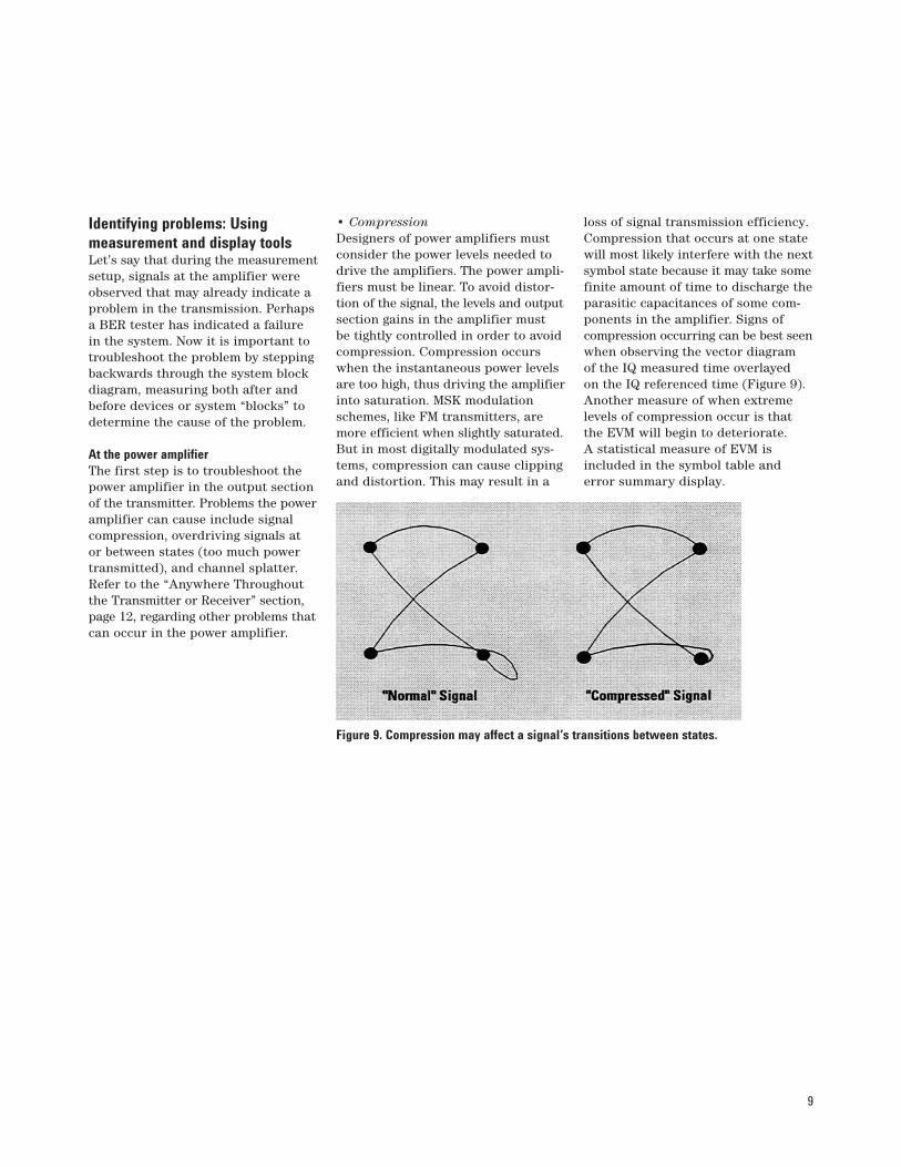
• CompressionDesigners of power amplifiers mustconsider the power levels needed todrive the amplifiers. The power ampli-fiers must be linear. To avoid distor-tion of the signal, the levels and outputsection gains in the amplifier must be tightly controlled in order to avoidcompression. Compression occurswhen the instantaneous power levelsare too high, thus driving the amplifierinto saturation. MSK modulationschemes, like FM transmitters, aremore efficient when slightly saturated.But in most digitally modulated sys-tems, compression can cause clippingand distortion. This may result in a
loss of signal transmission efficiency.Compression that occurs at one statewill most likely interfere with the nextsymbol state because it may take somefinite amount of time to discharge theparasitic capacitances of some com-ponents in the amplifier. Signs ofcompression occurring can be best seenwhen observing the vector diagram of the IQ measured time overlayed on the IQ referenced time (Figure 9).Another measure of when extremelevels of compression occur is thatthe EVM will begin to deteriorate. A statistical measure of EVM isincluded in the symbol table anderror summary display.
Figure 9. Compression may affect a signal’s transitions between states.
10
• Power splatterPower splatter can be caused byamplifier distortion which results inpower in adjacent channels. In analogmodulation systems (and even insome digital modulation systems),third- and fifth-order intermodulationrejection or similar tests have beenused in the past to measure amplifierdistortion. These CW (continuouswave) analog tests may not be validrepresentations of splatter in digitallymodulated systems where much higherorder distortion products can play a significant role in adjacent channelsplatter. Another potential concernfor digital systems is that the basestations may actually have several signals randomly added together andmeasuring the distortion of individualsignals may not accurately reflect thecomposite result. Especially in digitalsystems, it is best to determine ifsplatter is occurring by measuring theadjacent channel power (ACP) directly.
Swept LO techniques for measuringACP presume essentially stationarysignals and are not well suited fortime-variant signals. “Gated sweep”approaches improve this situation butat the cost of greatly increased sweeptimes. Also, these gated sweep tech-niques assume repetitive signals.
The Agilent 89400 Series VSAs havefrequency-selective, band powermarkers which can measure the powerof specific channels. Furthermore,these analyzers avoid the concernsand restrictions of swept LO or gatedtechniques by digitizing the entire signal. The signal processing in the89400 Series VSAs can characterizerapidly changing signals—this is impor-tant when dealing with burst signals.
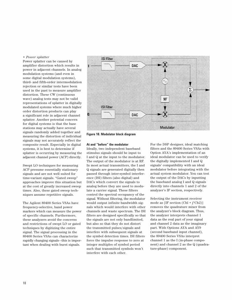
At and “before” the modulatorIdeally, two independent basebandstimulus signals should be input to I and Q at the input to the modulator.The output of the modulator is at RF.In most actual transmitters, the I andQ signals are generated digitally thenpassed through inter-symbol interfer-ence (ISI) filters (also digital) andDACs which convert the signals toanalog before they are used to modu-late a carrier signal. These filters control the spectral occupancy of thesignal. Without filtering, the modulatorwould output infinite bandwidth sig-nals which would interfere with otherchannels and waste spectrum. The ISIfilters are designed specifically so thatthe signals are not only bandlimited,but also so that they do not distortthe transmitted pulses/signals andinterfere with subsequent signals atthe symbol detection times. ISI filtersforce the impulse response to zero atinteger multiples of symbol periodsuch that transmitted symbols won’tinterfere with each other.
For the DSP designer, ideal matchingfilters and the 89400 Series VSAs withOption AYA’s implementation of anideal modulator can be used to verifythe digitally implemented I and Q signals’ compatibility with an idealmodulator before integrating with theactual system modulator. You can testthe output of the DACs by inputtingthe baseband analog I and Q signalsdirectly into channels 1 and 2 of theanalyzer’s IF section, respectively.
Selecting the instrument receivermode as [IF section (Chl + j*Ch2)]removes the quadrature mixer fromthe analyzer’s block diagram. Thus,the analyzer interprets channel 1 data as the real part of your signaland channel 2 data as the imaginarypart. With Options AYA and AY9 (second baseband input channel), the 89400 Series VSAs interpret channel 1 as the I (in-phase compo-nent) and channel 2 as the Q (quadra-ture-phase) component.
Figure 10. Modulator block diagram

11
Traditional swept spectrum analyzersprovide good numerical characteriza-tions of much of a modulator’s per-formance during the design phase.Measurements that can be madeinclude linearity and distortion, amongothers. The Agilent 89400 Series VSAsalso make these measurements (spec-trum mode) and can show the perform-ance characteristics visually, such asshifted constellation diagrams (refer to “Gain Imbalance and QuadratureError,” page 13). In addition, due tothe digitizing and signal processingtechniques used by the 89400 SeriesVSAs, phase information is preserved.Therefore, phase can be measured atthe output of the mixers and through-out the modulator. Simply phase lockthe analyzer to the modulator’s LOreference and measure the phase ofeach channel (I or Q input) relative to the LO. These measurements are a method of directly measuring thephase balance relative to the LO foreach channel throughout the mixersand modulator. Pulses in the poweramplifier (such as when transmittinginformation from a mobile to a baseunit) can adversely affect the phaseand/or frequency stability of the LO.
The quick and large level changes canaffect how the transmitted signal ishandled and may result in high EVM.For example, this may happen becausethe turn-on pulse can drain largeamounts of instantaneous currentfrom the power supply. In smalltransmitters such as handheld radios,because of the close proximity ofcomponents, large signals in the pres-ence of smaller ones may cause mag-netic couplings between circuits. Thesecouplings could cause distortion inthe signals being transmitted.
It is possible to measure the phasestability of the LO by synchronizing thePM demodulation measurement withthe transmitter pulses. Essentially, thisresults in a measure of instantaneousphase versus time. Typically, sync signals (control logic lines such as“Tx_on”) are available in radios. Suchsync signals can be used when deter-mining the frequency stability of theLO by measuring instantaneous fre-quency versus time (FM demodulation).
Some mobile radios receive and trans-mit signals at different frequencies.Also, commands may be sent from the
base station to the mobile unit direct-ing it to change frequencies for a quickhand-off to the next base station. TheLO of the modulator contains a phase-locked loop (PLL) to maintain fre-quency stability. The closed-loopresponse of the PLL determines howfast the LO can change frequencies.The 89400 Series VSAs can directlymeasure the closed-loop response ofthe modulator’s PLL in the correctdomain-modulation. An external signalgenerator which is modulated usingthe analyzer’s built-in source servesas a baseband reference input signalfor the PLL. The analyzer’s demodu-lator is applied at the output of thePLL which is translated up in fre-quency. The closed-loop response ismeasured and displayed directly andthe open-loop response can be derivedusing the analyzer’s built-in mathfunctions. The benefit is that you don’thave to tap into the loop or open it.Product Note 89400-6, TranslatedFrequency Response MeasurementsUsing the Agilent 89440A providesdetails on this measurement and others used to characterize the performance of PLLs.

12
Anywhere throughout the transmitter or receiverErrors can occur anywhere throughoutthe transmitter or receiver which canimpair the signal or data integrity. Anexample is when LO feedthrough cancause the symbol detector thresholdto be set incorrectly thus causing thewrong states and bits to be detected.Other typical sources of error includegain or phase imbalances, interferingor spurious signals, jamming, noise,symbol timing errors, amplitude orphase nonlinearities, carrier frequencyoffset, and AM to PM conversions.
A skillful eye can easily detect manytypes of errors by using the flexibledisplay formatting (such as overlayingtraces) and comparing measured signals to their ideal counterparts.
However, for faster and more conclu-sive determination of problems, aquantitative measure is most benefi-cial. The error vector magnitude(time) trace (Figure 11) is the bestmeasure of signal quality and shouldbe used whenever troubleshootingthrough a system.
Vertical bars or dots can be activatedto identify the symbol locations. TheEVM trace identifies when errorsoccur during the signal’s transmission.This trace can show whether errorsoccur at one or a few particular statesor during the transition between them.By tracking this measure when trouble-shooting at several points, you canlook for consistencies or patterns inerrors to help locate the cause.
These errors typically do not get anybetter (EVM does not get smaller) asa signal progresses down the system’stransmission path. X-axis scaling canbe used to spread out closely spacedpoints to ease viewing. EVM is impor-tant because at each point in the sig-nal train where the measurement ismade, the contribution to the overall“error budget” is characterized. Anoverall measure of EVM (% rms overall symbol detection/clock locations)is included in the error summarytable. The remaining paragraphs inthis product note describe examplesof other troubleshooting techniquesthat can be used to detect some of thetypical transmitter or receiver errorsthat occur.
Figure 11. Error vector time and x-axis scaled displays: the top trace shows how the measured signal varies from the ideal both at and between symbols and decision times (shown by the vertical bars); and the bottom trace shows an expanded view of the area delineated by the vertical band markers in the upper trace.

13
Gain imbalance and quadrature errorConstellation diagrams can often tellyou many things about the character-istics of signal impairments. Gainimbalance or quadrature errors canbe caused by matching problems dueto component differences (filters,DACs, etc.) between the I side and Q side of a network. Imbalances canalso be caused by errors in IF filtering,for example, when a filter responseisn’t flat. These errors may be due toAM to PM conversion as well and canresult in constellation distortion and,therefore, an increase in EVM. To detecteven subtle imbalances, view the con-stellation diagram of the IQ measuredtime and compare with the “idealgrids” (crossed lines in Figure 12).
The ideal grids indicate where theideal reference states should occur. IQgain imbalance results in a distortedmeasured constellation relative to
the reference. IQ quadrature errors(other than 90° between I and Q)result in a “tipped” or skewed con-stellation. Without the ideal grids, it would be very difficult to detectimbalances. Even subtle imbalancesare often visually detected by zoomingin (magnifying the scale) on the con-stellation and using the markers.Figure l3 illustrates gain imbalance(the gain of Q is low relative to 1) andquadrature error. In each, the dottedlines represent the ideal (reference)constellation.
The analyzer can help determine thecorrect orientation of the symbolstates by using a sync search with a defined sync word. This ability can assist you in determining the relative levels of I and Q such that the appropriate adjustments can bemade in the system. In other words,you can determine whether or not
the gain of I is low relative to that of Q,or vice versa. Refer to “Setting Up the Measurements—Pulse ModulatedSignals” on page 18 for informationon using sync search.
Instantaneous power— at and between symbolsVector diagrams show a signal’s tran-sitions between symbol states. Themagnitude of a vector between theorigin of the IQ complex plane andthe trace at any point corresponds to the instantaneous power level. Thisis an excellent way to observe andmeasure levels that may be detrimentalto parts of the system, such as over-driving a transmitter. By stacking thevector display on the upper trace withthe symbol table on the lower traceand coupling the markers, you cansee where any excessive signal levelsoccurred and the detected bits (the ls and 0s received) for the symbols.
Figure 13. Imbalance or quadrature errorswill often distort the shape of constellations.
Figure 12. A constellation diagram with ideal grids. Note how easily the distortion fromideal state locations is visible.

14
This may indicate a particular symbolpattern or state transition that is caus-ing the error. As mentioned earlier inthis product note, the symbol table(Figure 5d) also includes an errorsummary which displays quantitativemeasures of the quality of the signalreceived that could lead to bit errors.The statistics or error measures includeEVM (% rms and peak including sym-bol location), IQ phase and magnitudeerrors, carrier frequency error, ampli-tude droop, and IQ origin offset.
Interfering signals, feedthrough, and noiseAn interfering signal can cause theamplitude and phase of the transmittedsignal to be different each time thesignal passes through the same state.This will result in a spread at thesymbol locations in the constellationdiagram. It may be useful to determinewhat (and where) the quantitativeerror is by observing the IQ magnitudeerror or IQ phase error diagrams.Symbol spread can also be caused byinter-symbol interference, noise, originoffset, and symbol timing errors.
A “circling” of the symbols around theconstellation states indicates thatthere may be a spur or interferingtone. The radius of the circle is pro-portional to the amplitude of theinterfering signal, but this display format contains no information aboutthe interfering frequency which maybe the key to identifying the cause. To determine the presence of aninterfering signal, first verify that thesymbol timing recovery is correct byviewing the eye diagrams and look
to see if the eye crossings occur otherthan at the symbol “lines.” Next,observe the IQ measurement error(linear magnitude and phase) dis-plays. Watch for any characteristicsor signs of periodicity to the error or bursting and pulsing effects.
Close-in and low-level spurs on digi-tally modulated carriers cannot beseen on a spectrum analyzer. This isbecause the digitally modulated sig-nals look a lot like a random noisepedestal. Their presence may be diffi-cult at times to determine on a con-stellation display.
The EVM trace may hint that the errorobserved is sinusoidal in nature, butwhat is really needed is a method todetermine the frequency of the spur.The error vector spectrum indicatesany spurious signals which may be offset from the carrier. Refer toFigure 8 (page 7) and “MeasurementConcepts” (page 4).
IQ offset (a shift in the origin of the IQplane) is a measure of LO feedthroughin a transmission system and typicallyneeds to meet some specification.Although reported in the error sum-mary, the 89400 Series VSAs withOption AYA compensate for this errorboth graphically and mathematically(except when demodulating GSM sig-nals). Any offset does not appear inthe constellation or vector diagrams.LO feedthrough typically occurs at RFbut can also occur elsewhere in thesystem. This measure can indicateproblems such as imbalance due to a bad mixer or extraneous dc terms.
When first integrating a system, cou-pling and interference mechanismswhich do not occur in the ideal systemsimulations may appear and createproblems. A few common problemsinclude couplings between digital andanalog sections, system nonlinearities,power supply interference, and envi-ronmental effects such as temperaturedrift. The 89440A with the optionalsecond 10-MHz input channel (OptionAY7) and its coherence measurementhelp to locate the sources of variousinterference and feedthrough prob-lems. In many cases, simply using theRF input and AM, FM, or PM demodu-lation gives a picture which lets yourecognize a problem’s source by thesignal’s characteristics.
Coherence measurements isolate to a particular source of the problem.Figure 14 shows an example of how a noise source can be located. The RF input channel connected to thecarrier was PM demodulated, whilethe second 10-MHz channel was usedto probe around at various points in the system. The built-in coherencefunction then compares the two signals and gives a value between 0 (no coherence) and 1 (completecoherence) in the frequency domain.The closer the coherence is to a valueof one, the greater the probability thatthe two signals are directly related. In this case, obviously, the noise atlocation 2 is coherent with the PMdemodulation of the carrier. Coherencemeasurements can be used to locatethe cause of other sources of error as well.

15
Setting up the measurementsThis section describes how to set upmeasurements on vector (digitally)modulated signals when using theAgilent 89400 Series VSAs. An over-view of the procedure is to first, setup an appropriate input range andfrequency span. Then, connect the RFinput channel to the desired carrieror IF, or connect the two 10-MHzinput channels (assumes Option AY7second baseband channel is installed)to two independent baseband I and Qsignals. Next, select the signal’s mod-ulation format and symbol rate (typi-cally predefined by the system beingtested). Enter the number of symbolsdesired for analysis, and choose froma selection of ISI filter types withadjustable alpha. Finally, view andmeasure using a variety of displayformats with flexible scaling andmarkers. The four basic steps are con-nect [inputs], tune [span], select [mod-ulation format], and view [display].
Connect . . .The block diagram in Figure 15 will be used as a reference for the hard-ware connections used to troubleshootthroughout a system. Each of the geo-metrical shapes in this diagram corre-spond to the matching analyzer inputswhich are used for measurements.
Measurements can be performed at anyof these locations to isolate the causeof signal degradation. When measuringbaseband I and Q input signals directlyinto channels 1 and 2, set the analyzer’sreceiver (a softkey in the InstrumentMode hardkey menu) for the IF sectionequal to [Chl + j*Ch2].
Figure 14. Using the second 10-MHz input to probe two baseband locations, PM demodu-lation on the RF input, and coherence to compare them, the noise source is determined tobe location 2.
Figure 15. The analyzer’s inputs used to measure at various points in a system block diagram from baseband to RF.

16
Tune . . .Measure the antenna’s received signalover the air by connecting an antennaor cable to the analyzer’s RF input. Setthe analyzer for Vector InstrumentMode and the center frequency to bethe transmitter carrier frequency. A narrow frequency span should beused to reject extraneous noise; how-ever, the span must also be wideenough to view the full power spec-trum and for the analyzer to obtaincarrier lock. The analyzer automati-cally locks to a carrier signal withoutthe necessity of providing an externalcoherent carrier. Typically, the centerfrequency used in the measurementsshould be within 2% of the symbolclock frequency to achieve and main-tain lock. (Some modulation formatssuch as π/4DQPSK can lock with acenter frequency tolerance of less than
approximately 10% of the symbol clockrate.) For example, if the symbol clockfrequency is 10 kHz, then 2% is 200 Hz.Therefore, the center frequency mustbe within 200 Hz of the true carrierfrequency of the signal. A guidelinefor determining the appropriate ana-lyzer frequency span is:
The “span factor” is 1.28 and is relatedto the analyzer’s internal sample rate.Alpha is the shape factor (or rolloff) ofthe ISI filter being used. For example,using the NADC standard, the symbolrate is 24.3 kHz and alpha is 0.35,therefore the frequency span must beless than approximately 380 kHz butgreater than 32.8 kHz.
For burst or pulsed signals, triggeringis needed. IF triggering is a form ofenvelope triggering and looks formagnitude changes in the signal. It is impossible to trigger off of CW(continuous wave, or sinusoidal) orconstant envelope signals since theirmagnitude does not change. Also,
IF triggering does not work on somedigital signals because their powerlevels fluctuate during state transi-tions. If an external trigger signal(TTL level) is available in the systemit can be used to trigger the measure-ment. (Refer to the “Select” section on the next page regarding demodu-lating pulsed signals.)
After the instrument mode, analyzer’sreceiver type, center frequency, fre-quency span, and triggering are set,observe the power spectrum of thetransmitted signal to confirm that youare looking at the correct signal andverify that the system is operating.This is also a good preliminary indi-cator of system problems. Assumingthat the transmitted digitally modu-lated signal looks like noise, and giventhat the inter-symbol interference(ISI) filter shape used is known, thepower spectrum should look approxi-mately like the shape of the filter(Figure 16). Now, it is possible andconvenient to look for problems at theside lobes of the power spectrum usingx-axis scaling to measure the turn-onand turn-off characteristics of thetransmitter. Product Note 89400-5,Measuring Transmitter Transientswith the 89440A describes how to capture transient signals and how tomake instantaneous power, frequency,and phase measurements on such signals.
Figure 16. Power spectrum of a NADC signal with band-power markers. The true RMS-power detection and precise noise bandwidths in the 89400 Series VSAs provide theaccuracy and versatility needed to measure modern digital communication signals.
20*(Symbol rate) > Frequency span > (1 + alpha)(Symbol rate)
1.28
17
Select . . .Demodulate the incoming signal byselecting the appropriate modulationformat. Press in order the keys [Digitaldemodulation], [Demodulation setup],[Demod format] and select one of themany modulation formats supported.If you are using either NADC, PDC, or GSM formats, the one-key standardsetup configurations automaticallyset the analyzer for the correct modu-lation format, symbol rate, frequency
span, measured and reference filtertypes, alpha (or BT) and a predeter-mined number of symbols (resultlength). Any or all of these variablescan be set manually when using non-standard modulation formats.
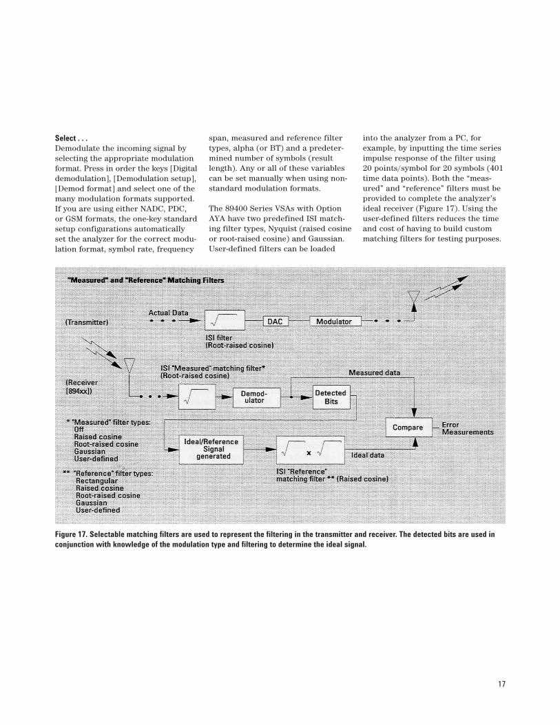
The 89400 Series VSAs with OptionAYA have two predefined ISI match-ing filter types, Nyquist (raised cosineor root-raised cosine) and Gaussian.User-defined filters can be loaded
into the analyzer from a PC, forexample, by inputting the time seriesimpulse response of the filter using20 points/symbol for 20 symbols (401time data points). Both the “meas-ured” and “reference” filters must beprovided to complete the analyzer’sideal receiver (Figure 17). Using theuser-defined filters reduces the timeand cost of having to build custommatching filters for testing purposes.
Figure 17. Selectable matching filters are used to represent the filtering in the transmitter and receiver. The detected bits are used inconjunction with knowledge of the modulation type and filtering to determine the ideal signal.
18
Pulsed modulated signalsTypically, such as for many TDMA andE-TDMA systems, the signals from amobile unit to the base station arepulsed. In other words, the carrierturns on and off. On being when thereceiver transmits data and off whenit finishes transmitting data. In theseinstances, it is important to measureonly during the information of interest.To verify that a pulsed signal is beingmeasured, first set the analyzer forVector mode and the display format tomain time. Look for pulses or bursts.When using digital demodulationmode, “pulse search” is an advancedtriggering capability which detectsthe leading and trailing edges of apulsed carrier with a non-constantenvelope characteristic. Pulse searchis a toggled softkey in the [Time] hard-key menu of the analyzer. It is similarto IF triggering in that it enables theanalyzer to identify pulses that occurwithin a time record. IF triggeringwill falsely trigger in the middle of apulsed carrier with a non-constantenvelope characteristic.
When you select pulse search on, theanalyzer searches for carrier turn-on,and then continues to search for car-rier turn-off. The analyzer displays“Pulse not found” if it does not detecta carrier. In other words, the analyzermust find the entire pulse (off to on,then on to off).
If a single measurement contains morethan one pulse, the analyzer examinesonly the first pulse. It ignores all otherpulses in the measurement. This situ-ation can occur for large search lengths.The search length (user definable)determines how much data the ana-lyzer collects. Use triggering and “syncsearch” to align the desired pulse nearthe beginning of the search record.“Sync search” (also under the [Time]hardkey) aligns the bits to be analyzedrelative to a specified sync word.
Shipped with vector modulation analy-sis (Option AYA) is a utility that usesan editor in the analyzer to assigncustom softkeys to quickly switchbetween several different sync wordsthat may be used for a specific modu-lation format. This utility is also impor-tant in that it allows the user to rede-fine the analyzer’s default state loca-tion assignments on constellation andvector diagrams. To view what thedefault state assignments are on theanalyzer, select in order [InstrumentMode], [Digital Demodulation],[Demod format], [State definitions].
Sync search is valid whether usingpulse search or not. In other words,sync search can be used to positionthe analysis region for either contin-uous or pulsed signals. When usingsync search, make sure the searchlength is large enough to capture theentire pulse, including any guard andramp bits. For best results, set thesearch length to at least 1.5 times the length of the pulse. The searchlength must be set to be longer thanthe amount of information to bedemodulated and displayed (theresult length). That is, you will beinstructing the analyzer to searchover at least the number of symbolsbeing analyzed. Refer to the analyzer’shelp text for more information regard-ing search length.
Finally, an offset (in number of sym-bols) can be defined in conjunctionwith the sync word to determine thelocation of the data to be demodulated(result length) within the amount ofdata collected (search length). Figure18 illustrates these concepts. Searchlength and result length are defined bypressing the [Time] hardkey. Offset is defined by pressing [Time] followedby [Sync setup]. This softkey menulevel is also where the sync pattern isdefined. If sync search is on and theanalyzer cannot find your sync pattern,the analyzer displays the message“Sync Not Found.”

19
View . . .The flexible display and marker for-matting of the Agilent 89400 SeriesVSAs with Option AYA makes locat-ing errors easy. Observe one, two(stacked or overlayed), or four(stacked or quad) color displayssimultaneously. Couple the markersbetween them to locate where certainsymbols translate into errors, forexample.
Several methods exist in the analyzerfor detecting errors in a transmittedsignal. Examples include using the“ideal grids” or overlaying like dis-plays (such as constellations of IQtime) to look for deviations of themeasured signal from the ideal refer-ence signal. X-axis scaling can beused to resolve closely spaced infor-mation in the measurement trace.However, the best methods for accu-
rately detecting errors are by usingthe error measurements—error vectormagnitude (time), error vector spec-trum, IQ error magnitude, and IQerror phase. These measurementswere discussed in the “MeasurementConcepts” section of this productnote (page 4).
Figure 18. Pulse search and sync search can be used when measuring bursted signals.

20
Generating digitally modulated signalsThe Agilent 89410A includes a built-in baseband source (and the 89440Ahas an optional RF source) that canbe used as a stimulus for digitallymodulated systems and demodulatedby the analyzer. Fixed sine, noise,chirp, and arbitrary signal types areavailable. For arbitrary signals, a8192 real (4096 complex) point timerecord of any measured signal can berecorded and played back as stimulus.The same time record is played overand over contiguously. Although thisis not representative of continuousdata or “live” signals, it may be inmany cases sufficient for testing.
Creating the arbitrary sourceTo generate a digitally modulatedsource signal, you can use a softwarepackage to create the data mathemat-ically and load it into the analyzer’sarbitrary source from a computer usingthe Standard Data Format Utilities(supplied standard with each 89400Series VSA). Examples of these soft-ware packages include MATLAB, a product of The Mathworks, andMathCAD, a product of Mathsoft.Alternatively, you can measure yourown test signal, save it to a data reg-ister, and output it via the arbitrarysource. You can also generate a digi-tally modulated source signal within
the analyzer by using the demodulatedideal reference signal (Figure 17). This signal will be output via the arbitrary source. It will consist of one time record that is played contin-uously and repeatedly. The procedurefor creating the source internally is as follows:
1. Preset the analyzer and select vector mode.
2. Set the desired center frequency(usually equal to the approximatecarrier frequency).
3. Set the frequency span. A span oftwo or three times the symbol rateis a good guideline. This step is notnecessary for generating the refer-ence signal, but it will be importantin the analysis of the signal.
4. Disconnect all signal inputs fromthe analyzer. Only input noise willbe used to generate the referencesignal.
5. Set the instrument mode for DigitalDemodulation. Using the softkeysin the Demodulation Setup menuselect the desired modulationparameters such as modulationtype, symbol rate, and alpha/BT.
6. For systems with distributed trans-mitter and receiver raised-cosine
(Nyquist) filtering, set both the Measurement Filter and theReference Filter as “Root” filter.The filter type setups are also inthe Demodulation Setup softkeymenu. For all other systems, a good guideline is to choose thereference filter setting to be thesame as the filtering that is usedfor the actual system transmitter.In generating a reference signalusing this procedure, only the ref-erence filter affects the result.
7. The Result Length should be set to be 25 symbols longer than thenumber of symbols that are to beanalyzed.
8. The number of Points/Symbolshould be a minimum of five (5).This minimum is adequate for manysignals, but those using Gaussianfiltering and a BT greater than 0.3 will require more. Ten to 20points/symbol is recommended,especially where BT is muchgreater than 0.3.
9. Set the Measurement Data to be IQReference Time and the Data For-mat for Constellation. You shouldsee large, noisy imperfections.
10. Save this IQ reference time traceinto a file or data register. Signalgeneration is now complete.

21
Measuring a signal (using thearbitrary source)1. The analyzer should be set accord-
ing to steps 1-3 and 5 in the pro-cedure outlined previously for cre-ating digitally modulated signals.
2. Using a cable, connect the sourceoutput to the analyzer’s input.Turn the analyzer’s source on andselect Source Type as Arbitrary.The arbitrary data register usedshould be the one where the digi-tally modulated signal was saved.If the signal was instead saved to a file, then recall the file to a data register.
3. Set the input range to the lowestvalue that does not result in anoverload condition. To do this,select [Range] and repeatedlypress the down arrow (in thenumeric keypad on the frontpanel) until the green overloadindicator light turns on. Then,press the up arrow once (until the overload light turns off).
4. Systems which used raised-cosine(Nyquist) filtering should use theanalyzer’s raised cosine referencemeasurement filter. In systemsthat use Gaussian filtering, set the reference filter type to Gaussian.Applications that use a user-definedfilter should use this same filteras the reference filter.
5. Also as part of the demodulationsetup, set the Result Length to beat least 25 symbols less than wasused to generate the signal.
6. Change the Trigger type to InternalSource. Use a Trigger Delay thatcorresponds to approximately 20 symbols. This delay will needto be set as a unit of time. To
determine the equivalent time corresponding to 20 symbols, display Measurement Data as IQ Measured Time and the DataFormat as Log or Linear Magnitude.Select the softkey More Data Formatand then select “dots” or “bars.”These dots or bars that are nowdisplayed indicate each symbol.Using the marker and the frontpanel knob, scroll over 20 symbols.If the marker’s x value currentlyreads in “units of seconds,” youwill need to change it to “units ofsymbols” by pressing in order thekeys [Ref Level/Scale], [X & Yunits setup], [X units]. Now togglefrom seconds to symbols. Usingthe knob, scroll out 20 symbols,then toggle back to seconds. Usethis time as the trigger delay.
7. The signal can be demodulatedjust as any “live” signal by settingthe defined signal parameters via Measurement Data and Data Format.
Other toolsIn time capture mode, the analyzersamples the input and stores theinformation in RAM. Up to 1 Msampleof one-channel data can be recorded(with Option AY9 extended time cap-ture) and 500 ksamples of two-chan-nel baseband data (using the receivertype [Chl + j*Ch2]) can be recorded.This data can then be transferred tothe internal floppy disk drive or to anexternal drive for postprocessing inthe analyzer either back in the lab or at another site. All of the on-linemeasurements can be made on cap-tured data. Although these measure-ments can be made on time captureddata, this data cannot be played back(in full) through the source output.Only one of the time records (8192real points or 4096 complex points)
can be played back via the arbitrarysource output. Product Note 89400-10,Time Capture Capabilities of the89400 Series Vector Signal Analyzers,provides more information on thisuseful tool.
View the analyzer’s display in realtime from across the building oracross the world using Options UG7(advanced LAN) and UFG (4-Mbytesextended RAM and additional I/O).Operating as an X Windows applica-tion, a 89400 Series VSA can open adisplay window on a user-designatedX Windows server anywhere on thenetwork. The X Windows display notonly shows the actual measurementtraces, but also simulates the analyzer’sfront panel. To operate the analyzerfrom a remote workstation, simplypress the desired keys with the mouseor other pointing device. Now, anR&D lab can assist in troubleshootingproblems at a manufacturing siteacross the country.
Finally, a few more features roundout the application. The analyzer cansave and recall important measure-ment setups and traces to memory or to disk. With Instrument BASIC(Option 1C2), keystroke recording canbe used to create custom measurementswhich can be accessed with softkeysbuilt into the program. The operatingmanual (“Help Text”) is built into theanalyzer and includes theory of oper-ation, setup descriptions, and a fullindex. And, report generation is simpleby direct output to a large array ofAgilent Technologies peripherals, orby printing or plotting to DOS filesthat can be easily incorporated intoword processing packages.
22
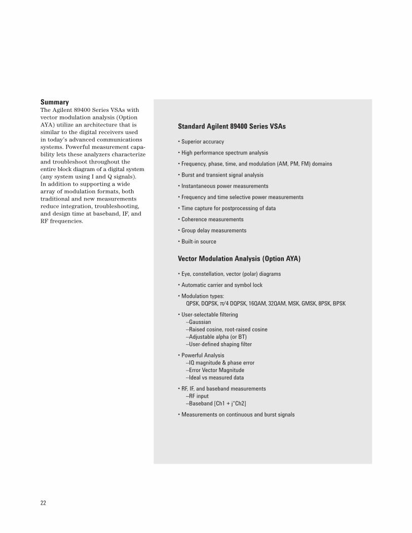
SummaryThe Agilent 89400 Series VSAs withvector modulation analysis (OptionAYA) utilize an architecture that issimilar to the digital receivers used in today’s advanced communicationssystems. Powerful measurement capa-bility lets these analyzers characterizeand troubleshoot throughout theentire block diagram of a digital system(any system using I and Q signals). In addition to supporting a widearray of modulation formats, bothtraditional and new measurementsreduce integration, troubleshooting,and design time at baseband, IF, andRF frequencies.
Standard Agilent 89400 Series VSAs
• Superior accuracy
• High performance spectrum analysis
• Frequency, phase, time, and modulation (AM, PM, FM) domains
• Burst and transient signal analysis
• Instantaneous power measurements
• Frequency and time selective power measurements
• Time capture for postprocessing of data
• Coherence measurements
• Group delay measurements
• Built-in source
Vector Modulation Analysis (Option AYA)
• Eye, constellation, vector (polar) diagrams
• Automatic carrier and symbol lock
• Modulation types: QPSK, DQPSK, π/4 DQPSK, 16QAM, 32QAM, MSK, GMSK, 8PSK, BPSK
• User-selectable filtering–Gaussian–Raised cosine, root-raised cosine–Adjustable alpha (or BT)–User-defined shaping filter
• Powerful Analysis–IQ magnitude & phase error–Error Vector Magnitude–Ideal vs measured data
• RF, IF, and baseband measurements–RF input–Baseband [Ch1 + j*Ch2]
• Measurements on continuous and burst signals

23
To make the measurements described in this product note, the following configuration is strongly recommended:
89440A 1.8 GHz vector signal analyzer (or the 89410A dc to 10 MHz vector signal analyzer)
Option AYA Vector modulation analysis
Option AY7 Second 10-MHz input channel
Option UFG 4-Mbytes extended RAM and additional I/O
Option AY9 Extend time capture to 1 Msample
For measurements above 1.8 GHz,the following configuration is strongly recommended:
89410A dc to 10 MHz vector signal analyzer
Option AYA Vector modulation analysis
Option AY7 Second 10-MHz input channel
Option UFG 4-Mbytes extended RAM and additional I/O
Option AY9 Extend time capture to 1 Msample
89411A 21.4 MHz down-converter
Spectrum analyzer with a 21.4 MHzIF (for example, the Agilent 8566B orthe 70000 Series)
The following options may be useful and included in the configurations above:
Option AY8 RF Source
Option UG7 Advanced LAN support
Configuration Guide

24
ACP: Adjacent channel power. Thepower in specified frequency bands iseasily measured with the band powermarkers in the Agilent 89400 SeriesVSAs. Also refer to Agilent ProductNote 89400-1 in the References.
Alpha or BT (bandwidth time product):The filter shape factor; also called theroll-off. The smaller the alpha, thesharper the filter. If alpha equals zero(a brick wall filter), the bandwidthequals the symbol rate. The actualbandwidth required in the carriersection (the occupied bandwidth) isequal to: (symbol rate)*(l + alpha).
Amplitude droop: Also called “burstamplitude droop.” A measure of thechange in the magnitude of the signalat the detection-decision points overthe measured burst in units of dB persymbol. This parameter is most signif-icant for pulsed signals. A high numbermost likely indicates a problem withthe pulse modulation process.
Band power: The total power (betweentwo selected frequencies or times)with units of dBm, dBVrms, Watts orVrms2.
BT (bandwidth time product):See Alpha.
Carrier frequency error: This parameteris a measure of the frequency errorbetween the measured IF signal andthe expected IF signal. Errors in the RF frequency, LO frequency ordigitizer clock rate could all appearas carrier frequency error.
Carrier lock: The 89400 series VSAsautomatically lock to carrier signalswithout providing an external coher-ent carrier. The center frequency ofthe analyzer should be set to be with-in 5% of the symbol clock frequencyto achieve and maintain lock.
Center frequency: This frequency shouldtypically be set to the modulation carrier frequency.
Coherence: A two-channel measurementthat indicates the similarity betweentwo signals. Specifically, it measuresthe power in the output signal causedby the input. A value of 1.0 equalsperfect coherence (all of the outputpower is caused by the input signal)whereas a value less than 1.0 mayindicate the presence of extraneousnoise, system nonlinearities or unexpected input signals.
Constellation diagram: A polar mappingof the state positions on the IQ plane.Constellation diagrams reveal spurioussignals as states in a circular pattern(rotating) around (versus a cluster at) their ideal positions at the symboldecision timing points. Here, the fre-quency of the spur is directly propor-tional to a vector if drawn radiallyfrom the ideal state position to thecircle (actual measured states). Close-in spurs are difficult to identify usingthis technique. Also, this same vectoris equivalent to the error vector. Thespectrum of this vector as it variesover time is called the error vectorspectrum.
Error Vector Magnitude (EVM): The mag-nitude of the vector drawn between theideal (reference) state position andthe measured state position. Twonumbers are measured, % rms andpeak (with the symbol number dis-played for the peak position).
Error vector spectrum: The frequencyspectrum of the error vector time.This measurement clearly identifiesthe frequencies of close-in spurioussignals present in a digital modula-tion system.
Error vector time: This measurementshows the error vector magnitudevariations as a signal changes overtime—that is, at and between symboldecision timing points.
Eye diagrams: A mapping of I (or Q)magnitude versus time wrappedaround a defined number of symbols.Traditionally, these diagrams havebeen measured with an oscilloscopewhich is triggered at the timinginstants. On the 89400 Series VSAs,the symbol clock detection points are represented by vertical lines onthe display.
Eye length: The number of symbolsthat the eye diagram displays (wrapsaround).
Glossary
25
Filter shape: The shape of the receiver’sfilter (ISI) used to match the trans-mitter’s filter (example: “root-raised-cosine”). For many modulation types,two receiver filters are used—the“measured” filter is the same as thatused at the transmitter whereas the“reference” filter is the squared productof the filter used at the transmitter.
Ideal (reference) signal: Also called theIQ reference signal. This is the signalthat would result after demodulatingyour signal if your signal were ideal(contained no errors). It is the idealsignal against which the IQ measuredsignal is compared for all of the errormeasurements (EVM, error vectortime, error vector spectrum, IQ errormagnitude, and phase). The 89400Series VSAs create this signal fromthe detected bits and knowledge ofthe filtering used, modulation format,symbol rate, etc.
IF trigger: A form of envelope triggering.Looks for magnitude/power levelchanges in each time record of thesignal measured. IF triggering is diffi-cult on some digital signals becausetheir power levels tend to fluctuate asthe signal transitions between states.It is also not possible to trigger onCW or fixed amplitude signals such as MSK formats. In these cases, if anexternal trigger signal (TTL) is avail-able in the system it can be used totrigger the measurement. Or, whenperforming vector demodulation, con-sider using pulse and/or sync search.
Input range: The 89400 Series VSAs havespecified ranges of allowable inputlevels (see the technical data sheet).These ranges should be set to maxi-mize the sensitivity to the input signal.To assist this process the analyzershave half-range and overload indicatorLEDs next to each input channel. Onemethod to set the range is to step downthe input range until the overloadindicator comes on, then step the rangeback up once or until the overload LEDis off. Some signals which are too lowfor the analyzer to measure, may needto be amplified prior to inputtingthem into the analyzer. The oppositeis true for signals which are too large,here attenuation is necessary.
IQ error (magnitude error): The magni-tude of the vector of the measuredstate and the magnitude of the vectorof the ideal (reference) state witheach vector having been drawn fromthe IQ plane origin. Two numbers aremeasured, % rms and peak (with thesymbol number displayed for thepeak position).
IQ error (phase error): The anglebetween the vector of the measuredstate and the vector of the ideal (ref-erence) state with each vector havingbeen drawn from the IQ plane origin.Two numbers are measured in degreesand % magnitude (with the symbolnumber displayed for the peak position).
IQ offset: Also called “IQ origin offset.”It is the magnitude of the carrier feed-through signal, relative to the magni-tude of the modulated carrier at thedetection decision points. Carrierfeedthrough is an indication of thebalance of the IQ modulator used to generate the modulated signal.Imbalance in the modulator results in carrier feedthrough and appears as a dc offset on the demodulated IQ signal.
ISI filter: The I and Q signals are gen-erated digitally then passed throughan inter-symbol interference (ISI) filter before being converted to ananalog signal which is modulated.Without filtering, the modulatorwould output infinite bandwidth signals which cannot be transmitted.The ISI filters are designed specificallyso that the signals are not only band-limited, but also so that they do notdistort the transmitted pulses/signalsand interfere with subsequent signals.ISI filters force the impulse responseto zero at integer multiples of symbolssuch that transmitted symbols won’tinterfere with each other.
Magnitude error: See IQ error.
Measurement filter: The ISI matchingfilter applied in the 89400 Series VSAs.This filter should be selected to matchthe filter used when transmitting thedata. Selectable filter types includeraised cosine, root-raised cosine,Gaussian, user-defined, and “off.” The“off” filter type is used in systemssuch as MSK which do not transmitwith an ISI filter in order to obtain(controlled/ desired) inter-symbolinterference. Another term sometimesused for the measurement filter is“half filter.”
26
Offset (QPSK or other): Some radio andsatellite systems use so called offsetkeyed or staggered modulation. Inthese systems a delay of half a symbol-time is introduced between the I andQ data streams, so that the modulationenvelope is not synchronized on bothI and Q carriers. This has the advan-tage of slightly reducing the peakpower handled by the transmitter.
Phase error: See IQ error.
Pulse search: Searches through thetransmitted data for pulses of data(such as transmit signals from mobileunits to base stations). When pulsesearch is used, sync search with adefined sync word must also be usedto help the analyzer to identify thedesired pulse.
Quadrature error: A measure of theerror from the ideal quadrature (90degree) angle between I and Q.
Reference filter: The filter applied inthe 89400 Series VSAs to match theISI filter used in a system’s receiver.This filter is typically the squaredproduct of the filter used to transmitthe data (transmit filter)2. Anotherterm sometimes used for the referencefilter is “whole filter.”
Result length: The total amount of data(symbols) displayed. The maximumnumber of symbols that can be dis-played in the 89400 Series VSAs is4096 (assuming Option UFG 4-Mbyteextended RAM is installed).
Search length: The total amount ofdata (symbols) that is demodulated.This amount must be greater than theamount of information displayed(result length).
Symbol lock: The 89400 Series VSAs canlock to symbols transmitted at ratesup to 6.36 MHz measuring with the89440A (9.09 MHz with the 89410A).
Symbol rate: The rate at which the carrier moves between points in theconstellation. For example, if a radiooperates at a frequency of 16 Mbits/second, and the digital modulationformat uses 4 bits/ state, then thecarrier must change states at a rate of4 MBaud, so the symbol rate = 4 MHz.
Symbol table and error summary: Thisdisplay has two parts. The upper por-tion is the error summary which dis-plays various measured parametersof the received signal. Included are:EVM (% rms and % peak at symbol #),magnitude error (% rms and % peakat symbol #), phase error (degreesand peak degrees at symbol #), fre-quency (carrier) error, IQ offset, andamplitude droop. The lower portionof this display is a table of the bits ofthe symbols, in ls and 0s, detected bythe receiver (the 89400 Series VSA).The maximum number of symbolsdisplayed is defined by the “resultlength” selected. If sync search isused, the sync word will be highlightedwhen detected (otherwise, the message“sync not found” will be shown inpart of the display).
Sync offset: The offset (in symbols) fromthe sync word used to define the startof the result or information displayed.
Sync word: A specific bit pattern locatedwithin the transmitted data streamthat is typically used to align the bitsand locate the information of interest.
Time capture: Continuous streams ofdata are sampled and passed directlyto time-capture RAM (maximum = 1Msamples) for postprocessing. Whenpostprocessing, all of the measurementsavailable in “normal” operation andon-line measurements are possible.
Time record: A block of time data sam-ples used to calculate each measure-ment. The length of the time record isvariable and is inversely proportionalto the frequency span (stop frequencyminus start frequency) selected.
Trellis diagram: A mapping of phaseversus time which is wrapped arounda defined number of symbols. On the89400 Series VSAs, the symbol clockdetection points are represented byvertical lines on the display. Trellisdiagrams are a useful means of showingthe phase trajectory at each symbol.
User-defined filter: ISI matching filterswhich can be downloaded into the89400 Series VSAs. Also see MeasuredFilter and Reference Filter.
Vector diagram: A polar mapping of thestate positions and the transitionalpaths (signal power) between thestates on the IQ plane.
27
Agilent Product Note 89400-1, Frequency and Time-Selective Power Measurementswith the Agilent 89400 Series Vector Signal Analyzers (p/n 5091-7194E).
Agilent Product Note 89400-2, Measuring Phase Noise with the Agilent 89400Series Vector Signal Analyzers (p/n 5091-7193E).
Agilent Product Note 89400-4, Characterization of Digital CommunicationsChannels with the Agilent 89400 Series Vector Signal Analyzers (p/n 5091-7195E).
Agilent Product Note 89400-5, Measuring Transmitter Transients with theAgilent 89440A Vector Signal Analyzer (p/n 5091-7235E).
Agilent Product Note 89400-6, Translated Frequency Response MeasurementsUsing the Agilent 89440A Vector Signal Analyzer (p/n 5091-7412E).
Agilent Product Note 89400A-9, Downconverted Measurements Using theAgilent 89410A and Agilent 89411A (p/n 5091-8691E).
Agilent Product Note 89400-10, Time Capture Capabilities of the Agilent89400 Series Vector Signal Analyzers (p/n 5091-8686E).
Agilent Application Note 355A, Digital Radio Theory and Measurements(p/n 5091-4777E).
Vector Signal Analyzers for Difficult Measurements on Time-Varying and Complex Modulated Signals, Hewlett-Packard Journal, December 1993,Ken J. Blue, Robert T. Cutler, Dennis P. O’Brien, Douglas R. Wagner, andBenjamin R. Zarlingo.
A Firmware Architecture for Multiple High-Performance Measurements,Hewlett-Packard Journal, December 1993, Dennis P. O’Brien.
Baseband Vector Signal Analyzer Hardware Design, Hewlett-Packard Journal,December 1993, Manfred Bartz, Keith A. Bayern, Joseph R. Deiderichs, andDavid F. Kelley.
RF Vector Signal Analyzer Hardware Design, Hewlett-Packard Journal,December 1993, Robert T. Cutler, William J. Ginder, Timothy L. Hillstrom,Kevin L. Johnson, Roy L. Mason, and James Pietsch.
Raymond A. Birgenheier, Measuring the Modulation Accuracy of π/4 DQPSKSignals for Digital Cellular Transmitters, Hewlett-Packard Journal, April 1991.
David Crim and William Turney of Motorola Inc., Radio Technology ResearchDept., Signal Analyzer Facilitates TDMA System Design, Microwaves & RF,April 1993.
Gary Sgrignoli of Zenith Electronics Corporation, Measuring Peak/AveragePower Ratio of the Zenith/AT&T DSC-HDTV Signal with a Vector SignalAnalyzer, IEEE Transactions on Broadcast, June 1993.
References

Adjacent channel power (ACP), 10, 24Alpha, 15–17, 24AM to PM conversion, 12,13Amplitude droop, 6,14, 24Antenna (measuring at the), 16Background, 2Bandwidth time product (BT).
See Alpha.Bit error rate (BER), 8Bit pattern detected, 6, 14Burst/pulsed signals (also see
pulse search), 8, 10, 11, 16, 18Carrier frequency, 7, 16, 24Carrier frequency error, 14, 24Carrier lock, 16, 24Ch1 + j*Ch2. See Measuring
baseband I & Q.Coherence,14, 24Compression, 9Configuration, 23Constellation diagram, 3, 13, 14, 24Error summary 5, 6, 14, 26Error vector magnitude
(EVM), 6, 7, 9, 11, 12, 14, 24Error vector spectrum, 7, 14, 24Eye diagram, 5, 6, 7, 24Filters (matching), 10, 17, 25FM demodulation, 11, 14Frequency span, 16Gain imbalance, 13Hardware connections, 15Ideal grids, 13Identifying problems, 9–14IF filtering, 13Imbalance (also see Gain imbalance
Quadrature error), 12, 13Intermodulation distortion, 10Inter-symbol interference, 14IQ measurement, 14IQ offset, 14, 25ISI filters. See Filters (matching).LAN, 21LO feedthrough, 12, 14LO stability (measuring), 11Magnitude error, 6Markers (band power), 10, 16, 24Markers (coupled), 6Measurement concepts, 4Measuring baseband I and Q, 10, 15
Memory requirements, 4Modulation concepts, 3, 4Modulation formats, 4Modulator, 10, 11Noise, 14, 20Offset (symbol), 18Origin offset. See 1Q offset.Other tools, 21Phase error, 6, 26Phase-locked loops, 11Phase stability, 11PM demodulation, 11, 14Points per symbol, 4, 17Post-processing. See time capture.Power (measuring), 4, 9, 16Power splatter, 8–10Pulse search, 18, 26Pulsed signals. See Burst signals.Quadrature error, 11, 13, 26Receiver (ideal), 17Reference (ideal) signal, 6, 20, 25Result length, 18, 26Saturation, 9Search length, 18, 26Setting up the measurements, 15Source (built-in), 20, 21Spectrum analyzers, 7, 11Spurious signals, 7, 14Standard setups, 17State locations (redefining), 18Summary, 22Symbol clock detection, 6Symbol rate, 4, 16, 26Symbol spread, 14Symbol table, 5, 6, 13, 26Symbol timing errors, 12,14Symbol timing recovery, 14Symbols (“circling”), 7, 14Symbols (maximum number), 4Sync (search, etc.), 13, 18, 26Time capture, 21, 26Transmission rate, 4Transmitter transients, 17Trellis diagram, 5, 6, 26Triggering, 16, 18, 25User-defined filters, 17, 26Vector diagram, 4, 5, 9,13, 26X Windows, 21X-axis scaling, 12,17
Agilent Technologies’ Test and MeasurementSupport, Services, and AssistanceAgilent Technologies aims to maximize the value you receive, while minimizingyour risk and problems. We strive toensure that you get the test and measure-ment capabilities you paid for and obtainthe support you need. Our extensive sup-port resources and services can help youchoose the right Agilent products for yourapplications and apply them successfully.Every instrument and system we sell has a global warranty. Support is available forat least five years beyond the productionlife of the product. Two concepts underlieAgilent’s overall support policy: “OurPromise” and “Your Advantage.”
Our Promise“Our Promise” means your Agilent test andmeasurement equipment will meet its adver-tised performance and functionality. Whenyou are choosing new equipment, we willhelp you with product information, includ-ing realistic performance specifications andpractical recommendations from experi-enced test engineers. When you use Agilentequipment, we can verify that it worksproperly, help with product operation, andprovide basic measurement assistance forthe use of specified capabilities, at noextra cost upon request. Many self-helptools are available.
Your Advantage“Your Advantage” means that Agilent offersa wide range of additional expert test andmeasurement services, which you can pur-chase according to your unique technicaland business needs. Solve problems effi-ciently and gain a competitive edge by con-tracting with us for calibration, extra- costupgrades, out-of-warranty repairs, and on-site education and training, as well asdesign, system integration, project man-agement, and other professional services.Experienced Agilent engineers and techni-cians worldwide can help you maximizeyour productivity, optimize the return oninvestment of your Agilent instruments andsystems, and obtain dependable measure-ment accuracy for the life of those products.
Get assistance with all your test and measurement needs at: www.agilent.com/find/assist
Product specifications and descriptions in this document subject to change without notice.
Copyright © 1994, 2000 Agilent TechnologiesPrinted in U.S.A. 9/005091-8687E
Index